WO2024176294A1 - 直流電源装置 - Google Patents
直流電源装置 Download PDFInfo
- Publication number
- WO2024176294A1 WO2024176294A1 PCT/JP2023/005959 JP2023005959W WO2024176294A1 WO 2024176294 A1 WO2024176294 A1 WO 2024176294A1 JP 2023005959 W JP2023005959 W JP 2023005959W WO 2024176294 A1 WO2024176294 A1 WO 2024176294A1
- Authority
- WO
- WIPO (PCT)
- Prior art keywords
- load
- power supply
- power
- supply device
- input terminal
- Prior art date
- Legal status (The legal status is an assumption and is not a legal conclusion. Google has not performed a legal analysis and makes no representation as to the accuracy of the status listed.)
- Ceased
Links
Images

Classifications
-
- H—ELECTRICITY
- H02—GENERATION; CONVERSION OR DISTRIBUTION OF ELECTRIC POWER
- H02J—ELECTRIC POWER NETWORKS; CIRCUIT ARRANGEMENTS OR SYSTEMS FOR SUPPLYING OR DISTRIBUTING ELECTRIC POWER; SYSTEMS FOR STORING ELECTRIC ENERGY
- H02J7/00—Circuit arrangements for charging or discharging batteries or for supplying loads from batteries
-
- H—ELECTRICITY
- H02—GENERATION; CONVERSION OR DISTRIBUTION OF ELECTRIC POWER
- H02M—APPARATUS FOR CONVERSION BETWEEN AC AND AC, BETWEEN AC AND DC, OR BETWEEN DC AND DC, AND FOR USE WITH MAINS OR SIMILAR POWER SUPPLY SYSTEMS; CONVERSION OF DC OR AC INPUT POWER INTO SURGE OUTPUT POWER; CONTROL OR REGULATION THEREOF
- H02M3/00—Conversion of DC power input into DC power output
- H02M3/02—Conversion of DC power input into DC power output without intermediate conversion into AC
- H02M3/04—Conversion of DC power input into DC power output without intermediate conversion into AC by static converters
- H02M3/10—Conversion of DC power input into DC power output without intermediate conversion into AC by static converters using discharge tubes with control electrode or semiconductor devices with control electrode
- H02M3/145—Conversion of DC power input into DC power output without intermediate conversion into AC by static converters using discharge tubes with control electrode or semiconductor devices with control electrode using devices of a triode or transistor type requiring continuous application of a control signal
- H02M3/155—Conversion of DC power input into DC power output without intermediate conversion into AC by static converters using discharge tubes with control electrode or semiconductor devices with control electrode using devices of a triode or transistor type requiring continuous application of a control signal using semiconductor devices only
-
- H—ELECTRICITY
- H02—GENERATION; CONVERSION OR DISTRIBUTION OF ELECTRIC POWER
- H02M—APPARATUS FOR CONVERSION BETWEEN AC AND AC, BETWEEN AC AND DC, OR BETWEEN DC AND DC, AND FOR USE WITH MAINS OR SIMILAR POWER SUPPLY SYSTEMS; CONVERSION OF DC OR AC INPUT POWER INTO SURGE OUTPUT POWER; CONTROL OR REGULATION THEREOF
- H02M7/00—Conversion of AC power input into DC power output; Conversion of DC power input into AC power output
- H02M7/02—Conversion of AC power input into DC power output without possibility of reversal
- H02M7/04—Conversion of AC power input into DC power output without possibility of reversal by static converters
- H02M7/12—Conversion of AC power input into DC power output without possibility of reversal by static converters using discharge tubes with control electrode or semiconductor devices with control electrode
Definitions
- An embodiment of the present invention relates to a DC power supply device.
- DC power supply devices that convert the power supplied from a power source into DC power appropriate for the load, and supply the converted DC power to the load.
- loads such as electrolytic cells that store energy internally and can become a DC power source when the DC power supply device stops operating.
- An embodiment of the present invention provides a DC power supply device that can suppress the inflow of energy from a load.
- a DC power supply device connected to a load that can be a DC power supply, the DC power supply device having a high potential output terminal connected to a high potential input terminal of the load and a low potential output terminal connected to a low potential input terminal of the load, a main circuit unit connected to a power supply, converting power supplied from the power supply into DC power appropriate for the load and supplying the converted DC power to the load, and a first rectifier element provided either between the high potential input terminal and the high potential output terminal or between the low potential input terminal and the low potential output terminal, for suppressing the flow of energy from the load to the main circuit unit.
- a DC power supply device that can suppress the inflow of energy from a load.
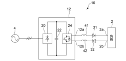
- FIG. 1 is a block diagram illustrating a DC power supply device according to an embodiment of the present invention
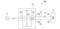
- FIG. 13 is a block diagram illustrating a modified example of a DC power supply device according to the embodiment.
- FIG. 13 is a block diagram illustrating a modified example of a DC power supply device according to the embodiment.
- FIG. 1 is a block diagram that illustrates a DC power supply device according to an embodiment.
- the DC power supply device 10 includes a main circuit unit 12, a first rectifier element 31, and a second rectifier element 32.
- the DC power supply device 10 is connected to a load 2 that can be a DC power supply.
- the load 2 has a high-potential input terminal 2a and a low-potential input terminal 2b.
- the load 2 is, for example, an electrolytic cell that generates products such as hydrogen by performing electrolysis in response to the supply of DC power from the DC power supply device 10.
- the high-potential input terminal 2a is an anode.
- the low-potential input terminal 2b is a cathode.
- the load 2 is not limited to an electrolytic layer and may be, for example, a storage battery.
- the load 2 may be any load that can become a DC power source when the operation of the DC power supply device 10 is stopped.
- the main circuit section 12 has a high-potential output terminal 12a connected to the high-potential input terminal 2a of the load 2, and a low-potential output terminal 12b connected to the low-potential input terminal 2b of the load 2.
- the main circuit section 12 is connected to the load 2 via the high-potential output terminal 12a and the low-potential output terminal 12b.
- the main circuit section 12 is also connected to the power source 4.
- the power source 4 is, for example, an AC commercial power source.
- the power supplied from the power source 4 to the main circuit section 12 is, for example, AC power.
- the power supplied from the power source 4 to the main circuit section 12 is not limited to AC power, and may be DC power or the like.
- the power source 4 may be any power source capable of supplying the power required by the DC power supply device 10.
- the main circuit unit 12 converts the power supplied from the power source 4 into DC power appropriate for the load 2, and supplies the converted DC power to the load 2.
- the main circuit unit 12 is, for example, an AC-DC conversion circuit that converts the AC power supplied from the power source 4 into DC power appropriate for the load 2.
- the main circuit section 12 has, for example, a rectifier circuit 20, a storage element 22, and a conversion circuit 24.
- the rectifier circuit 20 rectifies the AC power supplied from the power source 4.
- the rectifier circuit 20 is, for example, a diode bridge.
- the storage element 22 smoothes the power output from the rectifier circuit 20.
- the storage element 22 is, for example, a capacitor.
- the storage element 22 may be any element capable of smoothing the power output from the rectifier circuit 20.
- the conversion circuit 24 converts the power smoothed by the storage element 22 into DC power according to the load 2, and supplies the converted DC power to the load 2.
- the conversion circuit 24 is, for example, a DC-DC conversion circuit.
- the conversion circuit 24 may be configured in any way that is capable of converting DC power into another DC power according to the load 2.
- the main circuit unit 12 may be configured in any way that can convert the power supplied from the power source 4 into DC power appropriate for the load 2 and supply the converted DC power to the load 2.
- the rectifier circuit 20 is not limited to a diode bridge, and may be a circuit using switching elements such as IGBTs.
- the rectifier circuit 20 may be replaced with a circuit (e.g., a PWM circuit) that converts AC power into DC power of any magnitude by switching multiple switching elements.
- the first rectifier element 31 is provided either between the high potential input terminal 2a and the high potential output terminal 12a or between the low potential input terminal 2b and the low potential output terminal 12b, and suppresses the flow of energy from the load 2 to the main circuit section 12.
- the second rectifier element 32 is provided between the high potential input terminal 2a and the high potential output terminal 12a, and between the low potential input terminal 2b and the low potential output terminal 12b, and suppresses the flow of energy from the load 2 to the main circuit section 12.
- the first rectifier element 31 is provided between the high potential input terminal 2a and the high potential output terminal 12a
- the second rectifier element 32 is provided between the low potential input terminal 2b and the low potential output terminal 12b
- the first rectifier element 31 may be provided between the low potential input terminal 2b and the low potential output terminal 12b
- the second rectifier element 32 may be provided between the high potential input terminal 2a and the high potential output terminal 12a.
- the first rectifier element 31 and the second rectifier element 32 are, for example, diodes.
- the anode of the first rectifier element 31 is connected to the high potential output terminal 12a, and the cathode of the first rectifier element 31 is connected to the high potential input terminal 2a.
- the anode of the second rectifier element 32 is connected to the low potential input terminal 2b, and the cathode of the second rectifier element 32 is connected to the low potential output terminal 12b.
- the rectification of the first rectifier element 31 and the second rectifier element 32 allows the supply of DC power from the main circuit unit 12 to the load 2 while suppressing the inflow of energy from the load 2 to the main circuit unit 12.
- the reverse flow of DC power from the load 2 to the main circuit unit 12 can be suppressed.
- the flow of current from the high potential input terminal 2a toward the high potential output terminal 12a and the flow of current from the low potential output terminal 12b toward the low potential input terminal 2b can be suppressed.
- first rectifying element 31 and the second rectifying element 32 are not limited to diodes, and may be any element capable of suppressing the flow of energy from the load 2 to the main circuit section 12.
- the DC power supply device 10 further includes reactors 41, 42.
- the reactor 41 is provided between the first rectifier element 31 and the main circuit unit 12.
- the reactor 42 is provided between the second rectifier element 32 and the main circuit unit 12.
- the reactor 41 is provided between the first rectifier element 31 and the high-potential output terminal 12a of the main circuit unit 12
- the reactor 42 is provided between the second rectifier element 32 and the low-potential output terminal 12b of the main circuit unit 12.
- the reactors 41 and 42 for example, suppress switching noise superimposed on the DC power supplied from the main circuit unit 12 to the load 2.
- the reactors 41 and 42 suppress noise superimposed on the DC power supplied to the load 2, and smooth the current and voltage supplied to the load 2.
- the DC power supply device 10 includes a first rectifier element 31 and a second rectifier element 32, which suppress the inflow of energy from the load 2 to the main circuit unit 12.
- the DC power supply device 10 can suppress the inflow of energy from the load 2 even when connected to the load 2 that can become a DC power source.
- the DC power supply device 10 can suppress damage to equipment that would otherwise be caused by the inflow of energy from the load 2.
- the reactor 41 is provided between the first rectifier element 31 and the main circuit section 12. This makes it possible to more appropriately prevent damage to the reactor 41 caused by the inflow of energy from the load 2, compared to a case in which the reactor 41 is provided between the first rectifier element 31 and the load 2, for example.
- FIG. 2 is a block diagram that illustrates a modified example of the DC power supply device according to the embodiment. 2, in the DC power supply device 10a, the second rectifier element 32 is omitted. In this manner, the DC power supply device 10a may be configured to include only the first rectifier element 31. The second rectifier element 32 is provided as necessary and can be omitted. In this manner, even in a configuration including only the first rectifier element 31, it is possible to suppress the inflow of energy from the load 2 and suppress damage to equipment caused by the inflow of energy from the load 2.
- FIG. 3 is a block diagram that illustrates a modified example of the DC power supply device according to the embodiment.
- the first rectifier element 31 is provided between the low potential input terminal 2b and the low potential output terminal 12b.
- the inflow of energy from the load 2 can be suppressed, and damage to equipment caused by the inflow of energy from the load 2 can be suppressed.
- the first rectifier element 31 may be provided between the high potential input terminal 2a and the high potential output terminal 12a, or between the low potential input terminal 2b and the low potential output terminal 12b.
- the first rectifier element 31 may be provided either between the high potential input terminal 2a and the high potential output terminal 12a or between the low potential input terminal 2b and the low potential output terminal 12b.
- the first rectifier element 31 it is more preferable to provide the first rectifier element 31 between the high potential input terminal 2a and the high potential output terminal 12a, rather than between the low potential input terminal 2b and the low potential output terminal 12b.
- the first rectifier element 31 By providing the first rectifier element 31 only between the terminals on the high potential side in this way, the inflow of energy from the load 2 can be more appropriately suppressed, compared to a configuration in which the first rectifier element 31 is provided only between the terminals on the low potential side.
- the DC power supply device further includes a second rectifier element 32, as shown in FIG. 1. This makes it possible to more appropriately suppress the inflow of energy from the load 2, compared to a configuration including only the first rectifier element 31.
- a DC power supply device connected to a load that can be a DC power supply, a main circuit section having a high potential output terminal connected to a high potential input terminal of the load and a low potential output terminal connected to a low potential input terminal of the load, the main circuit section being connected to a power source, converting power supplied from the power source into DC power corresponding to the load, and supplying the converted DC power to the load; a first rectifier element provided either between the high potential input terminal and the high potential output terminal or between the low potential input terminal and the low potential output terminal, the first rectifier element suppressing a flow of energy from the load to the main circuit unit;
- a DC power supply device comprising:
- Reference Signs List 2 Load, 2a: High potential input terminal, 2b: Low potential input terminal, 4: Power source, 10, 10a, 10b: DC power supply device, 12: Main circuit section, 12a: High potential output terminal, 12b: Low potential output terminal, 20: Rectifier circuit, 22: Storage element, 24: Conversion circuit, 31: First rectifier element, 32: Second rectifier element, 41, 42: Reactor
Landscapes
- Engineering & Computer Science (AREA)
- Power Engineering (AREA)
- Rectifiers (AREA)
Abstract
直流電源になり得る負荷に接続される直流電源装置であって、前記負荷の高電位入力端子と接続される高電位出力端子と、前記負荷の低電位入力端子と接続される低電位出力端子と、を有するとともに、電源と接続され、前記電源から供給された電力を前記負荷に応じた直流電力に変換し、変換後の前記直流電力を前記負荷に供給する主回路部と、前記高電位入力端子と前記高電位出力端子との間及び前記低電位入力端子と前記低電位出力端子との間の一方に設けられ、前記負荷から前記主回路部へのエネルギーの流入を抑制する第1整流素子と、を備えた直流電源装置が提供される。これにより、負荷からのエネルギーの流入を抑制できる直流電源装置が提供される。
Description
本発明の実施形態は、直流電源装置に関する。
電源から供給された電力を負荷に応じた直流電力に変換し、変換後の直流電力を負荷に供給する直流電源装置がある。こうした直流電源装置に接続される負荷において、例えば電解槽など、内部にエネルギーを保存し、直流電源装置の運転停止時に直流電源になり得る負荷がある。
直流電源になり得る負荷に接続された直流電源装置において、運転停止時の直流電源装置の電位が、負荷の電位よりも低いと、負荷のエネルギーが直流電源装置に流入し、直流電源装置の破損などを招いてしまう恐れがある。また、直流電源装置に短絡破損が発生した場合には、直流電源装置内のエネルギーだけでなく、負荷からのエネルギーも流入してしまう可能性がある。この場合、アーク短絡が継続し、被害が拡大してしまう恐れがある。
このため、直流電源になり得る負荷に接続される直流電源装置においては、負荷からのエネルギーの流入を抑制できるようにすることが望まれる。
本発明の実施形態は、負荷からのエネルギーの流入を抑制できる直流電源装置を提供する。
本発明の実施形態によれば、直流電源になり得る負荷に接続される直流電源装置であって、前記負荷の高電位入力端子と接続される高電位出力端子と、前記負荷の低電位入力端子と接続される低電位出力端子と、を有するとともに、電源と接続され、前記電源から供給された電力を前記負荷に応じた直流電力に変換し、変換後の前記直流電力を前記負荷に供給する主回路部と、前記高電位入力端子と前記高電位出力端子との間及び前記低電位入力端子と前記低電位出力端子との間の一方に設けられ、前記負荷から前記主回路部へのエネルギーの流入を抑制する第1整流素子と、を備えた直流電源装置が提供される。
本発明の実施形態によれば、負荷からのエネルギーの流入を抑制できる直流電源装置が提供される。
以下に、各実施の形態について図面を参照しつつ説明する。
なお、図面は模式的または概念的なものであり、各部分の厚みと幅との関係、部分間の大きさの比率などは、必ずしも現実のものと同一とは限らない。また、同じ部分を表す場合であっても、図面により互いの寸法や比率が異なって表される場合もある。
なお、本願明細書と各図において、既出の図に関して前述したものと同様の要素には同一の符号を付して詳細な説明は適宜省略する。
なお、図面は模式的または概念的なものであり、各部分の厚みと幅との関係、部分間の大きさの比率などは、必ずしも現実のものと同一とは限らない。また、同じ部分を表す場合であっても、図面により互いの寸法や比率が異なって表される場合もある。
なお、本願明細書と各図において、既出の図に関して前述したものと同様の要素には同一の符号を付して詳細な説明は適宜省略する。
図1は、実施形態に係る直流電源装置を模式的に表すブロック図である。
図1に表したように、直流電源装置10は、主回路部12と、第1整流素子31と、第2整流素子32と、を備える。直流電源装置10は、直流電源になり得る負荷2に接続される。
図1に表したように、直流電源装置10は、主回路部12と、第1整流素子31と、第2整流素子32と、を備える。直流電源装置10は、直流電源になり得る負荷2に接続される。
負荷2は、高電位入力端子2aと、低電位入力端子2bと、を有する。負荷2は、例えば、直流電源装置10からの直流電力の供給に応じて電気分解を行うことにより、水素などの生成物の生成を行う電解槽である。高電位入力端子2aは、換言すれば、陽極である。低電位入力端子2bは、換言すれば、陰極である。但し、負荷2は、電解層に限ることなく、例えば、蓄電池などでもよい。負荷2は、直流電源装置10の運転停止時などに直流電源になり得る任意の負荷でよい。
主回路部12は、負荷2の高電位入力端子2aと接続される高電位出力端子12aと、負荷2の低電位入力端子2bと接続される低電位出力端子12bと、を有する。主回路部12は、高電位出力端子12a及び低電位出力端子12bを介して負荷2と接続される。
また、主回路部12は、電源4と接続される。電源4は、例えば、交流の商用電源である。電源4から主回路部12に供給される電力は、例えば、交流電力である。但し、電源4から主回路部12に供給される電力は、交流電力に限ることなく、直流電力などでもよい。電源4は、直流電源装置10に必要な電力を供給可能な任意の電源でよい。
主回路部12は、電源4から供給された電力を負荷2に応じた直流電力に変換し、変換後の直流電力を負荷2に供給する。主回路部12は、例えば、電源4から供給された交流電力を負荷2に応じた直流電力に変換するAC-DC変換回路である。
主回路部12は、例えば、整流回路20と、蓄電素子22と、変換回路24と、を有する。整流回路20は、電源4から供給された交流電力を整流する。整流回路20は、例えば、ダイオードブリッジである。
蓄電素子22は、整流回路20から出力された電力を平滑化する。蓄電素子22は、例えば、コンデンサなどである。蓄電素子22は、整流回路20から出力された電力を平滑化することが可能な任意の素子でよい。
変換回路24は、蓄電素子22によって平滑化された電力を負荷2に応じた直流電力に変換し、変換後の直流電力を負荷2に供給する。変換回路24は、例えば、DC-DC変換回路である。変換回路24の構成は、直流電力を負荷2に応じた別の直流電力に変換可能な任意の構成でよい。
但し、主回路部12の構成は、上記に限定されるものではない。主回路部12の構成は、電源4から供給された電力を負荷2に応じた直流電力に変換し、変換後の直流電力を負荷2に供給することが可能な任意の構成でよい。
例えば、整流回路20は、ダイオードブリッジに限ることなく、IGBTなどのスイッチング素子を用いた回路などでもよい。換言すれば、整流回路20は、複数のスイッチング素子のスイッチングによって交流電力を任意の大きさの直流電力に変換する回路(例えばPWM回路)などに置き換えてもよい。
第1整流素子31は、高電位入力端子2aと高電位出力端子12aとの間及び低電位入力端子2bと低電位出力端子12bとの間の一方に設けられ、負荷2から主回路部12へのエネルギーの流入を抑制する。
第2整流素子32は、高電位入力端子2aと高電位出力端子12aとの間及び低電位入力端子2bと低電位出力端子12bとの間の他方に設けられ、負荷2から主回路部12へのエネルギーの流入を抑制する。
この例では、第1整流素子31が、高電位入力端子2aと高電位出力端子12aとの間に設けられ、第2整流素子32が、低電位入力端子2bと低電位出力端子12bとの間に設けられている。これとは反対に、低電位入力端子2bと低電位出力端子12bとの間に第1整流素子31を設け、高電位入力端子2aと高電位出力端子12aとの間に第2整流素子32を設けてもよい。
第1整流素子31及び第2整流素子32は、例えば、ダイオードである。例えば、第1整流素子31のアノードが高電位出力端子12aと接続され、第1整流素子31のカソードが高電位入力端子2aと接続される。そして、第2整流素子32のアノードが低電位入力端子2bと接続され、第2整流素子32のカソードが低電位出力端子12bと接続される。これにより、第1整流素子31及び第2整流素子32の整流により、主回路部12から負荷2への直流電力の供給を許容しつつ、負荷2から主回路部12へのエネルギーの流入を抑制することができる。換言すれば、負荷2から主回路部12への直流電力の逆流を抑制することができる。高電位入力端子2aから高電位出力端子12aに向かう方向の電流の流れ、及び低電位出力端子12bから低電位入力端子2bに向かう方向の電流の流れを抑制することができる。
但し、第1整流素子31及び第2整流素子32は、ダイオードに限ることなく、負荷2から主回路部12へのエネルギーの流入を抑制可能な任意の素子でよい。
直流電源装置10は、リアクトル41、42をさらに備える。リアクトル41は、第1整流素子31と主回路部12との間に設けられる。リアクトル42は、第2整流素子32と主回路部12との間に設けられる。この例では、リアクトル41は、第1整流素子31と主回路部12の高電位出力端子12aとの間に設けられ、リアクトル42は、第2整流素子32と主回路部12の低電位出力端子12bとの間に設けられる。
リアクトル41、42は、例えば、主回路部12から負荷2に供給する直流電力に重畳するスイッチングノイズなどを抑制する。リアクトル41、42は、負荷2に供給する直流電力に重畳するノイズを抑制し、負荷2に供給する電流及び電圧を平滑化する。
第1整流素子31及び第2整流素子32を有しない直流電源装置では、直流電源装置の運転停止時などに負荷2が直流電源となり、負荷2のエネルギーが直流電源装置に流入し、直流電源装置の破損などを招いてしまう恐れがある。
これに対し、本実施形態に係る直流電源装置10は、第1整流素子31及び第2整流素子32を備え、第1整流素子31及び第2整流素子32が、負荷2から主回路部12へのエネルギーの流入を抑制する。これにより、直流電源装置10では、直流電源になり得る負荷2に接続される際にも、負荷2からのエネルギーの流入を抑制することができる。直流電源装置10では、負荷2からのエネルギーの流入にともなう機器の破損などを抑制することができる。
また、本実施形態に係る直流電源装置10では、リアクトル41が、第1整流素子31と主回路部12との間に設けられる。これにより、例えば、リアクトル41が第1整流素子31と負荷2との間に設けられる場合と比べて、負荷2からのエネルギーの流入にともなうリアクトル41の破損なども、より適切に抑制することができる。
図2は、実施形態に係る直流電源装置の変形例を模式的に表すブロック図である。
図2に表したように、直流電源装置10aでは、第2整流素子32が省略されている。このように、直流電源装置10aは、第1整流素子31のみを備えた構成でもよい。第2整流素子32は、必要に応じて設けられ、省略可能である。このように、第1整流素子31のみを備えた構成においても、負荷2からのエネルギーの流入を抑制し、負荷2からのエネルギーの流入にともなう機器の破損などを抑制することができる。
図2に表したように、直流電源装置10aでは、第2整流素子32が省略されている。このように、直流電源装置10aは、第1整流素子31のみを備えた構成でもよい。第2整流素子32は、必要に応じて設けられ、省略可能である。このように、第1整流素子31のみを備えた構成においても、負荷2からのエネルギーの流入を抑制し、負荷2からのエネルギーの流入にともなう機器の破損などを抑制することができる。
図3は、実施形態に係る直流電源装置の変形例を模式的に表すブロック図である。
図3に表したように、直流電源装置10bでは、第1整流素子31が、低電位入力端子2bと低電位出力端子12bとの間に設けられている。この場合にも、負荷2からのエネルギーの流入を抑制し、負荷2からのエネルギーの流入にともなう機器の破損などを抑制することができる。
図3に表したように、直流電源装置10bでは、第1整流素子31が、低電位入力端子2bと低電位出力端子12bとの間に設けられている。この場合にも、負荷2からのエネルギーの流入を抑制し、負荷2からのエネルギーの流入にともなう機器の破損などを抑制することができる。
このように、第1整流素子31のみを備える場合、第1整流素子31は、高電位入力端子2aと高電位出力端子12aとの間に設けてもよいし、低電位入力端子2bと低電位出力端子12bとの間に設けてもよい。第1整流素子31は、高電位入力端子2aと高電位出力端子12aとの間及び低電位入力端子2bと低電位出力端子12bとの間の一方に設けられていればよい。
但し、第1整流素子31は、低電位入力端子2bと低電位出力端子12bとの間よりも、高電位入力端子2aと高電位出力端子12aとの間に設けることがより好適である。このように、高電位側の端子間のみに第1整流素子31を設けることにより、低電位側の端子間のみに第1整流素子31を設ける構成と比べて、負荷2からのエネルギーの流入をより適切に抑制することができる。
また、直流電源装置は、図1に表したように、第2整流素子32をさらに備えることがより好適である。これにより、第1整流素子31のみを備える構成と比べて、負荷2からのエネルギーの流入をより適切に抑制することができる。
本実施形態は、以下の態様を含む。
(付記1)
直流電源になり得る負荷に接続される直流電源装置であって、
前記負荷の高電位入力端子と接続される高電位出力端子と、前記負荷の低電位入力端子と接続される低電位出力端子と、を有するとともに、電源と接続され、前記電源から供給された電力を前記負荷に応じた直流電力に変換し、変換後の前記直流電力を前記負荷に供給する主回路部と、
前記高電位入力端子と前記高電位出力端子との間及び前記低電位入力端子と前記低電位出力端子との間の一方に設けられ、前記負荷から前記主回路部へのエネルギーの流入を抑制する第1整流素子と、
を備えた直流電源装置。
(付記1)
直流電源になり得る負荷に接続される直流電源装置であって、
前記負荷の高電位入力端子と接続される高電位出力端子と、前記負荷の低電位入力端子と接続される低電位出力端子と、を有するとともに、電源と接続され、前記電源から供給された電力を前記負荷に応じた直流電力に変換し、変換後の前記直流電力を前記負荷に供給する主回路部と、
前記高電位入力端子と前記高電位出力端子との間及び前記低電位入力端子と前記低電位出力端子との間の一方に設けられ、前記負荷から前記主回路部へのエネルギーの流入を抑制する第1整流素子と、
を備えた直流電源装置。
(付記2)
前記高電位入力端子と前記高電位出力端子との間及び前記低電位入力端子と前記低電位出力端子との間の他方に設けられ、前記負荷から前記主回路部へのエネルギーの流入を抑制する第2整流素子をさらに備えた付記1記載の直流電源装置。
前記高電位入力端子と前記高電位出力端子との間及び前記低電位入力端子と前記低電位出力端子との間の他方に設けられ、前記負荷から前記主回路部へのエネルギーの流入を抑制する第2整流素子をさらに備えた付記1記載の直流電源装置。
(付記3)
前記第1整流素子と前記主回路部との間に設けられたリアクトルをさらに備えた付記1又は2に記載の直流電源装置。
前記第1整流素子と前記主回路部との間に設けられたリアクトルをさらに備えた付記1又は2に記載の直流電源装置。
(付記4)
前記負荷は、電解槽である付記1~3のいずれか1つに記載の直流電源装置。
前記負荷は、電解槽である付記1~3のいずれか1つに記載の直流電源装置。
本発明のいくつかの実施形態を説明したが、これらの実施形態は、例として提示したものであり、発明の範囲を限定することは意図していない。これら新規な実施形態は、その他の様々な形態で実施されることが可能であり、発明の要旨を逸脱しない範囲で、種々の省略、置き換え、変更を行うことができる。これら実施形態やその変形は、発明の範囲や要旨に含まれるとともに請求の範囲に記載された発明とその均等の範囲に含まれる。
2…負荷、 2a…高電位入力端子、 2b…低電位入力端子、 4…電源、 10、10a、10b…直流電源装置、 12…主回路部、 12a…高電位出力端子、 12b…低電位出力端子、 20…整流回路、 22…蓄電素子、 24…変換回路、 31…第1整流素子、 32…第2整流素子、 41、42…リアクトル
Claims (4)
- 直流電源になり得る負荷に接続される直流電源装置であって、
前記負荷の高電位入力端子と接続される高電位出力端子と、前記負荷の低電位入力端子と接続される低電位出力端子と、を有するとともに、電源と接続され、前記電源から供給された電力を前記負荷に応じた直流電力に変換し、変換後の前記直流電力を前記負荷に供給する主回路部と、
前記高電位入力端子と前記高電位出力端子との間及び前記低電位入力端子と前記低電位出力端子との間の一方に設けられ、前記負荷から前記主回路部へのエネルギーの流入を抑制する第1整流素子と、
を備えた直流電源装置。 - 前記高電位入力端子と前記高電位出力端子との間及び前記低電位入力端子と前記低電位出力端子との間の他方に設けられ、前記負荷から前記主回路部へのエネルギーの流入を抑制する第2整流素子をさらに備えた請求項1記載の直流電源装置。
- 前記第1整流素子と前記主回路部との間に設けられたリアクトルをさらに備えた請求項1記載の直流電源装置。
- 前記負荷は、電解槽である請求項1記載の直流電源装置。
Priority Applications (1)
| Application Number | Priority Date | Filing Date | Title |
|---|---|---|---|
| PCT/JP2023/005959 WO2024176294A1 (ja) | 2023-02-20 | 2023-02-20 | 直流電源装置 |
Applications Claiming Priority (1)
| Application Number | Priority Date | Filing Date | Title |
|---|---|---|---|
| PCT/JP2023/005959 WO2024176294A1 (ja) | 2023-02-20 | 2023-02-20 | 直流電源装置 |
Publications (1)
| Publication Number | Publication Date |
|---|---|
| WO2024176294A1 true WO2024176294A1 (ja) | 2024-08-29 |
Family
ID=92500429
Family Applications (1)
| Application Number | Title | Priority Date | Filing Date |
|---|---|---|---|
| PCT/JP2023/005959 Ceased WO2024176294A1 (ja) | 2023-02-20 | 2023-02-20 | 直流電源装置 |
Country Status (1)
| Country | Link |
|---|---|
| WO (1) | WO2024176294A1 (ja) |
Citations (8)
| Publication number | Priority date | Publication date | Assignee | Title |
|---|---|---|---|---|
| JPH10150773A (ja) * | 1996-11-15 | 1998-06-02 | Meidensha Corp | 制御用直流電源装置 |
| JPH1185294A (ja) * | 1997-09-12 | 1999-03-30 | Nippon Boshoku Kogyo Kk | 直流電源装置 |
| JP2000152502A (ja) * | 1998-11-09 | 2000-05-30 | Sumitomo Electric Ind Ltd | Pwm電流型電力変換器の高調波流入抑制方法 |
| JP2009232599A (ja) * | 2008-03-24 | 2009-10-08 | Kitakyushu Foundation For The Advancement Of Industry Science & Technology | 電源装置及びアーク溶接機 |
| JP4701689B2 (ja) * | 2004-05-28 | 2011-06-15 | 富士電機システムズ株式会社 | 電力システム |
| JP2011160656A (ja) * | 2011-05-24 | 2011-08-18 | Mitsubishi Electric Corp | 直流電源装置 |
| JP2014154437A (ja) * | 2013-02-12 | 2014-08-25 | Toshiba Corp | 試験システムおよび試験方法 |
| JP2021057944A (ja) * | 2019-09-27 | 2021-04-08 | 株式会社大原興商 | 電力供給方法 |
-
2023
- 2023-02-20 WO PCT/JP2023/005959 patent/WO2024176294A1/ja not_active Ceased
Patent Citations (8)
| Publication number | Priority date | Publication date | Assignee | Title |
|---|---|---|---|---|
| JPH10150773A (ja) * | 1996-11-15 | 1998-06-02 | Meidensha Corp | 制御用直流電源装置 |
| JPH1185294A (ja) * | 1997-09-12 | 1999-03-30 | Nippon Boshoku Kogyo Kk | 直流電源装置 |
| JP2000152502A (ja) * | 1998-11-09 | 2000-05-30 | Sumitomo Electric Ind Ltd | Pwm電流型電力変換器の高調波流入抑制方法 |
| JP4701689B2 (ja) * | 2004-05-28 | 2011-06-15 | 富士電機システムズ株式会社 | 電力システム |
| JP2009232599A (ja) * | 2008-03-24 | 2009-10-08 | Kitakyushu Foundation For The Advancement Of Industry Science & Technology | 電源装置及びアーク溶接機 |
| JP2011160656A (ja) * | 2011-05-24 | 2011-08-18 | Mitsubishi Electric Corp | 直流電源装置 |
| JP2014154437A (ja) * | 2013-02-12 | 2014-08-25 | Toshiba Corp | 試験システムおよび試験方法 |
| JP2021057944A (ja) * | 2019-09-27 | 2021-04-08 | 株式会社大原興商 | 電力供給方法 |
Similar Documents
| Publication | Publication Date | Title |
|---|---|---|
| JP5379248B2 (ja) | Dc/dc電力変換装置 | |
| JP5476400B2 (ja) | 電力変換装置、電力変換装置の制御方法、およびハードディスク装置 | |
| US9899910B2 (en) | Bridgeless PFC power converter with reduced EMI noise | |
| US7969752B2 (en) | Switching power supply device using current sharing transformer | |
| JP2014079168A (ja) | 電源装置 | |
| WO2021017390A1 (zh) | Dcdc环流控制装置、控制方法、电子设备、介质 | |
| KR101345282B1 (ko) | 대기모드 저전력이 가능한 전원공급장치 | |
| JP2016096591A (ja) | 絶縁形交流−直流変換装置 | |
| TW200402928A (en) | Power converter | |
| Li et al. | LED driver based on novel ripple cancellation technique for flicker‐free operation and reduced power processing | |
| WO2024176294A1 (ja) | 直流電源装置 | |
| JP7148205B1 (ja) | 電源回路、制御方法およびプログラム | |
| WO2018061077A1 (ja) | 電力変換装置 | |
| JP2012191761A (ja) | 交流−直流変換回路 | |
| JP2012239324A (ja) | Dc/dc電力変換装置 | |
| JP2017127045A (ja) | 電源システム | |
| JP2016123148A (ja) | スイッチング電源装置 | |
| US20080205108A1 (en) | Power Converter Apparatus | |
| CN112751328A (zh) | 直流供电系统 | |
| KR101330639B1 (ko) | 대기모드 저전력이 가능한 전원공급장치 | |
| JP7108526B2 (ja) | 電力変換装置 | |
| Srinithi et al. | Symmetric multilevel inverter using DC-DC zeta converter | |
| JP2005204463A (ja) | Dc−dcコンバータ | |
| WO2024241409A1 (ja) | 電解槽用電源装置 | |
| EP4496199A1 (en) | Converter for transferring power and corresponding method |
Legal Events
| Date | Code | Title | Description |
|---|---|---|---|
| 121 | Ep: the epo has been informed by wipo that ep was designated in this application |
Ref document number: 23923950 Country of ref document: EP Kind code of ref document: A1 |
|
| NENP | Non-entry into the national phase |
Ref country code: DE |
|
| 122 | Ep: pct application non-entry in european phase |
Ref document number: 23923950 Country of ref document: EP Kind code of ref document: A1 |