WO2024166718A1 - トランスチップ - Google Patents
トランスチップ Download PDFInfo
- Publication number
- WO2024166718A1 WO2024166718A1 PCT/JP2024/002553 JP2024002553W WO2024166718A1 WO 2024166718 A1 WO2024166718 A1 WO 2024166718A1 JP 2024002553 W JP2024002553 W JP 2024002553W WO 2024166718 A1 WO2024166718 A1 WO 2024166718A1
- Authority
- WO
- WIPO (PCT)
- Prior art keywords
- wiring
- coil
- pad
- transformer
- chip
- Prior art date
- Legal status (The legal status is an assumption and is not a legal conclusion. Google has not performed a legal analysis and makes no representation as to the accuracy of the status listed.)
- Ceased
Links
Images


Classifications
-
- H—ELECTRICITY
- H01—ELECTRIC ELEMENTS
- H01F—MAGNETS; INDUCTANCES; TRANSFORMERS; SELECTION OF MATERIALS FOR THEIR MAGNETIC PROPERTIES
- H01F27/00—Details of transformers or inductances, in general
- H01F27/28—Coils; Windings; Conductive connections
- H01F27/29—Terminals; Tapping arrangements for signal inductances
- H01F27/292—Surface mounted devices
-
- H—ELECTRICITY
- H01—ELECTRIC ELEMENTS
- H01F—MAGNETS; INDUCTANCES; TRANSFORMERS; SELECTION OF MATERIALS FOR THEIR MAGNETIC PROPERTIES
- H01F17/00—Fixed inductances of the signal type
-
- H—ELECTRICITY
- H01—ELECTRIC ELEMENTS
- H01F—MAGNETS; INDUCTANCES; TRANSFORMERS; SELECTION OF MATERIALS FOR THEIR MAGNETIC PROPERTIES
- H01F27/00—Details of transformers or inductances, in general
- H01F27/28—Coils; Windings; Conductive connections
-
- H—ELECTRICITY
- H01—ELECTRIC ELEMENTS
- H01F—MAGNETS; INDUCTANCES; TRANSFORMERS; SELECTION OF MATERIALS FOR THEIR MAGNETIC PROPERTIES
- H01F27/00—Details of transformers or inductances, in general
- H01F27/28—Coils; Windings; Conductive connections
- H01F27/2804—Printed windings
-
- H—ELECTRICITY
- H10—SEMICONDUCTOR DEVICES; ELECTRIC SOLID-STATE DEVICES NOT OTHERWISE PROVIDED FOR
- H10D—INORGANIC ELECTRIC SEMICONDUCTOR DEVICES
- H10D84/00—Integrated devices formed in or on semiconductor substrates that comprise only semiconducting layers, e.g. on Si wafers or on GaAs-on-Si wafers
- H10D84/01—Manufacture or treatment
- H10D84/02—Manufacture or treatment characterised by using material-based technologies
- H10D84/03—Manufacture or treatment characterised by using material-based technologies using Group IV technology, e.g. silicon technology or silicon-carbide [SiC] technology
- H10D84/038—Manufacture or treatment characterised by using material-based technologies using Group IV technology, e.g. silicon technology or silicon-carbide [SiC] technology using silicon technology, e.g. SiGe
-
- H—ELECTRICITY
- H10—SEMICONDUCTOR DEVICES; ELECTRIC SOLID-STATE DEVICES NOT OTHERWISE PROVIDED FOR
- H10W—GENERIC PACKAGES, INTERCONNECTIONS, CONNECTORS OR OTHER CONSTRUCTIONAL DETAILS OF DEVICES COVERED BY CLASS H10
- H10W90/00—Package configurations
-
- H—ELECTRICITY
- H01—ELECTRIC ELEMENTS
- H01F—MAGNETS; INDUCTANCES; TRANSFORMERS; SELECTION OF MATERIALS FOR THEIR MAGNETIC PROPERTIES
- H01F27/00—Details of transformers or inductances, in general
- H01F27/28—Coils; Windings; Conductive connections
- H01F27/2804—Printed windings
- H01F2027/2809—Printed windings on stacked layers
-
- H—ELECTRICITY
- H01—ELECTRIC ELEMENTS
- H01F—MAGNETS; INDUCTANCES; TRANSFORMERS; SELECTION OF MATERIALS FOR THEIR MAGNETIC PROPERTIES
- H01F27/00—Details of transformers or inductances, in general
- H01F27/28—Coils; Windings; Conductive connections
- H01F27/2804—Printed windings
- H01F2027/2819—Planar transformers with printed windings, e.g. surrounded by two cores and to be mounted on printed circuit
Definitions
- This disclosure relates to a transformer chip.
- Patent Document 1 describes an electronic component that includes a transformer chip having a primary coil and a secondary coil.
- a transformer chip includes an insulating layer including an upper surface and a lower surface facing opposite each other in the thickness direction, a first coil disposed within the insulating layer near the upper surface, a second coil disposed within the insulating layer near the lower surface and facing the first coil, and a first pad formed on the upper surface and electrically connected to the first coil, the first pad being disposed in an inner region surrounded by the first coil when viewed from the thickness direction, and including a first extension portion extending toward the first coil beyond a position 5 ⁇ m inward from the inner peripheral end of the first coil.
- the transformer chip which is one aspect of the present disclosure, can improve the dielectric strength voltage.
- FIG. 1 is a circuit diagram showing a schematic configuration of a signal transmission device according to an embodiment.
- FIG. 2 is a plan view that illustrates a schematic configuration of the signal transmission device of FIG.
- FIG. 3 is a cross-sectional view that illustrates a schematic configuration of the signal transmission device of FIG.
- FIG. 4 is a schematic perspective view showing a transformer chip of the signal transmission device of FIG.
- FIG. 5 is a schematic plan view of the transformer chip of FIG.
- FIG. 6 is a schematic plan view showing the second coil of the transformer chip of FIG.
- FIG. 7 is a schematic plan view showing a first coil of the transformer chip of FIG.
- FIG. 8 is a cross-sectional view taken along line 8-8 of FIG.
- FIG. 9 is a cross-sectional view taken along line 9-9 in FIG. FIG.
- FIG. 10 is an enlarged plan view of a portion of the first coil in FIG.
- FIG. 11 is a cross-sectional view taken along line 11-11 in FIG.
- FIG. 12 is a schematic cross-sectional view showing a simulation result of the electric field intensity in the transformer chip of FIG.
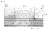
- FIG. 13 is a schematic cross-sectional view showing a simulation result of the electric field intensity in the transformer chip of the comparative example.
- FIG. 14 is a schematic plan view showing a transformer chip according to a modified example.
- FIG. 15 is an enlarged plan view of a portion of FIG.
- FIG. 16 is a partial schematic plan view showing a transformer chip according to a modified example.
- FIG. 17 is a schematic cross-sectional view showing a transformer chip according to a modified example.
- FIG. 18 is a schematic cross-sectional view showing a transformer chip according to a modified example.
- FIG. 19 is a schematic cross-sectional view showing a transformer chip according to a modified example.
- FIG. 20 is a partial schematic plan view showing a transformer chip according to a modified example.
- FIG. 21 is a schematic cross-sectional view of a part of the transformer chip shown in FIG.
- FIG. 22 is a partial schematic plan view showing a transformer chip according to a modified example.
- FIG. 23 is a schematic cross-sectional view of a part of the transformer chip shown in FIG.
- FIG. 24 is a schematic plan view showing a transformer chip according to a modified example.
- FIG. 25 is a schematic plan view showing a transformer chip according to a modified example.
- FIG. 25 is a schematic plan view showing a transformer chip according to a modified example.
- FIG. 26 is a schematic plan view showing a transformer chip according to a modified example.
- FIG. 27 is a circuit diagram showing a schematic configuration of a signal transmission device according to a modified example.
- FIG. 28 is a plan view that illustrates a schematic configuration of the signal transmission device of FIG.
- At least one means “one or more” of the desired options.
- at least one means “only one option” or “both of two options” if the number of options is two.
- at least one means “only one option” or “any combination of two or more options” if the number of options is three or more.
- FIG. 1 A schematic configuration of a signal transmission device 10 according to an embodiment will be described with reference to FIGS. 1 to 3.
- FIG. 1 A schematic configuration of a signal transmission device 10 according to an embodiment will be described with reference to FIGS. 1 to 3.
- FIG. 1 A schematic configuration of a signal transmission device 10 according to an embodiment will be described with reference to FIGS. 1 to 3.
- FIG. 1 A schematic configuration of a signal transmission device 10 according to an embodiment will be described with reference to FIGS. 1 to 3.
- FIG. 1 shows a schematic diagram of the circuit configuration of a signal transmission device 10 according to one embodiment.
- FIG. 2 shows a schematic diagram of an example of the internal configuration (planar structure) of the signal transmission device 10.
- FIG. 3 shows a schematic diagram of an example of a portion of the internal configuration (cross-sectional structure) of the signal transmission device 10. For convenience, hatched lines have been omitted from FIG. 3.
- the signal transmission device 10 is applied to an inverter device 500.
- the inverter device 500 includes a control circuit (ECU: Electronic Control Unit) 503, the signal transmission device 10, and switching elements 501 and 502.
- the signal transmission device 10 is used as a gate driver that drives the switching element 501 by the control circuit 503.
- FIG. 1 shows the signal transmission device 10 that drives the switching element 501.
- Switching element 501 is, for example, a high-side switching element connected to a drive power supply, and switching element 502 is a low-side switching element.
- switching elements 501 and 502 include transistors such as SiMOSFETs (Si Metal-Oxide-Semiconductor Field-Effect Transistors), SiCMOSFETs, and IGBTs (Insulated Gate Bipolar Transistors).
- the signal transmission device 10 applies a drive voltage signal to the control terminal of the switching element 501.
- a case where SiC MOSFETs are used as the switching elements 501 and 502 will be explained.
- the signal transmission device 10 is provided for each of the switching elements 501 and 502, and drives the switching elements 501 and 502 individually.
- the signal transmission device 10 includes a low-voltage circuit 20 to which a first voltage V1 is applied, a high-voltage circuit 30 to which a second voltage V2 higher than the first voltage V1 is applied, and a transformer 40 provided between the low-voltage circuit 20 and the high-voltage circuit 30.
- the low-voltage circuit 20 and the high-voltage circuit 30 are connected via the transformer 40.
- the first voltage V1 and the second voltage V2 are DC voltages.
- the signal transmission device 10 of this embodiment is configured so that a signal is transmitted from the low-voltage circuit 20 via the transformer 40 to the high-voltage circuit 30 based on a control signal from the control circuit 503, and a drive voltage signal is output from the high-voltage circuit 30.
- the signal transmitted from the low-voltage circuit 20 to the high-voltage circuit 30, i.e., the signal output from the low-voltage circuit 20, is, for example, a signal for driving the switching element 501, and examples include a set signal (SET) and a reset signal (RESET).
- the set signal is a signal that transmits the rising edge of a control signal from the control circuit 503, and the reset signal is a signal that transmits the falling edge of a control signal from the control circuit 503.
- the set signal and reset signal can also be said to be signals for generating a drive voltage signal for the switching element 501. For this reason, the set signal and reset signal correspond to the "first signal".
- the low-voltage circuit 20 is a circuit configured to operate when a first voltage V1 is applied.
- the low-voltage circuit 20 is electrically connected to the control circuit 503, and generates a set signal and a reset signal based on a control signal input from the control circuit 503.
- the low-voltage circuit 20 generates a set signal in response to a rising edge of the control signal, and generates a reset signal in response to a falling edge of the control signal.
- the low-voltage circuit 20 then transmits the generated set signal and reset signal to the high-voltage circuit 30.
- the high-voltage circuit 30 is a circuit configured to operate when the second voltage V2 is applied.
- the high-voltage circuit 30 is electrically connected to the gate of the switching element 501.
- the high-voltage circuit 30 generates a drive voltage signal for driving the switching element 501 based on the set signal and reset signal received from the low-voltage circuit 20, and applies the drive voltage signal to the gate of the switching element 501.
- the high-voltage circuit 30 generates a drive voltage signal to be applied to the gate of the switching element 501 based on the first signal output from the low-voltage circuit 20.
- the high-voltage circuit 30 generates a drive voltage signal that turns on the switching element 501 based on the set signal, and applies the drive voltage signal to the gate of the switching element 501.
- the high-voltage circuit 30 generates a drive voltage signal that turns off the switching element 501 based on the reset signal, and applies the drive voltage signal to the gate of the switching element 501. In this way, the signal transmission device 10 controls the on/off of the switching element 501.
- the high-voltage circuit 30 has, for example, an RS-type flip-flop circuit to which a set signal and a reset signal are input, and a driver section that generates a drive voltage signal based on the output signal of the RS-type flip-flop circuit.
- a driver section that generates a drive voltage signal based on the output signal of the RS-type flip-flop circuit.
- the specific circuit configuration of the high-voltage circuit 30 can be changed as desired.
- the low-voltage circuit 20 and the high-voltage circuit 30 are insulated by the transformer 40. More specifically, the transformer 40 restricts the transmission of DC voltage between the low-voltage circuit 20 and the high-voltage circuit 30, while allowing the transmission of various signals such as set signals and reset signals.
- the state in which the low-voltage circuit 20 and the high-voltage circuit 30 are insulated means that the transmission of DC voltage between the low-voltage circuit 20 and the high-voltage circuit 30 is blocked, while the transmission of signals between the low-voltage circuit 20 and the high-voltage circuit 30 is permitted.
- the dielectric strength voltage of the signal transmission device 10 is, for example, 2500 Vrms or more and 7500 Vrms or less.
- the dielectric strength voltage of the signal transmission device 10 in this embodiment is about 5000 Vrms.
- the specific value of the dielectric strength voltage of the signal transmission device 10 is not limited to this and can be any value.
- the ground GND1 of the low-voltage circuit 20 and the ground GND2 of the high-voltage circuit 30 are provided independently.
- the potential of the ground GND1 of the low-voltage circuit 20 is referred to as the first reference potential
- the potential of the ground GND2 of the high-voltage circuit 30 is referred to as the second reference potential.
- the first voltage V1 is a voltage from the first reference potential
- the second voltage V2 is a voltage from the second reference potential.
- the first voltage V1 is, for example, 4.5V or more and 5.5V or less
- the second voltage V2 is, for example, 9V or more and 24V or less.
- the signal transmission device 10 of this embodiment includes two transformers 40 corresponding to two signals transmitted from the low-voltage circuit 20 to the high-voltage circuit 30.
- one of the two transformers 40 is referred to as a transformer 40A
- the other of the two transformers 40 is referred to as a transformer 40B.
- the transformer 40A is used to transmit a set signal.
- the transformer 40B is used to transmit a reset signal.
- the set signal and the reset signal may be a set signal and a reset signal in a receiving circuit included in the high-voltage circuit 30.
- the signal transmission device 10 includes a low-voltage signal line 21A that connects the low-voltage circuit 20 and the transformer 40A, and a low-voltage signal line 21B that connects the low-voltage circuit 20 and the transformer 40B.
- the low-voltage signal line 21A transmits a set signal from the low-voltage circuit 20 to the transformer 40A.
- the low-voltage signal line 21B transmits a reset signal from the low-voltage circuit 20 to the transformer 40B.
- the signal transmission device 10 includes a high-voltage signal line 31A that connects the transformer 40A and the high-voltage circuit 30, and a high-voltage signal line 31B that connects the transformer 40B and the high-voltage circuit 30.
- the high-voltage signal line 31A transmits a set signal from the transformer 40A to the high-voltage circuit 30.
- the high-voltage signal line 31B transmits a reset signal from the transformer 40B to the high-voltage circuit 30.
- Transformer 40A transmits a set signal from low-voltage circuit 20 to high-voltage circuit 30 while electrically insulating low-voltage circuit 20 from high-voltage circuit 30.
- Transformer 40B transmits a reset signal from low-voltage circuit 20 to high-voltage circuit 30 while electrically insulating low-voltage circuit 20 from high-voltage circuit 30.
- Transformers 40A and 40B have a first coil 41 and a second coil 42.
- the first coil 41 and the second coil 42 are electrically insulated from each other and are configured to be magnetically coupled.
- the second coil 42 of the transformer 40A is connected to the low-voltage circuit 20 by the low-voltage signal line 21A, while it is connected to the ground GND1 of the low-voltage circuit 20. That is, the first end of the second coil 42 of the transformer 40A is electrically connected to the low-voltage circuit 20, and the second end of the second coil 42 of the transformer 40A is electrically connected to the ground GND1 of the low-voltage circuit 20.
- the second coil 42 of the transformer 40B is connected to the low-voltage circuit 20 by the low-voltage signal line 21B, while it is connected to the ground GND1 of the low-voltage circuit 20.
- the first reference potential is, for example, 0V.
- the first coil 41 of the transformer 40A is connected to the high-voltage circuit 30 by the high-voltage signal line 31A, and is also connected to the ground GND2 of the high-voltage circuit 30. That is, the first end of the first coil 41 of the transformer 40A is electrically connected to the high-voltage circuit 30, and the second end of the first coil 41 of the transformer 40A is electrically connected to the ground GND2 of the high-voltage circuit 30.
- the first coil 41 of the transformer 40B is connected to the high-voltage circuit 30 by the high-voltage signal line 31B, and is also connected to the ground GND2 of the high-voltage circuit 30.
- the first end of the first coil 41 of the transformer 40B is electrically connected to the high-voltage circuit 30, and the second end of the first coil 41 of the transformer 40B is electrically connected to the ground GND2 of the high-voltage circuit 30. Therefore, the potential of the second end of the first coil 41 of the transformers 40A and 40B becomes the second reference potential.
- the ground GND2 of the high-voltage circuit 30 is connected to the source of the switching element 501. Therefore, the second reference potential fluctuates as the inverter device 500 is driven, and may become, for example, 600 V or more.
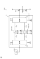
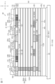
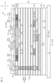
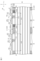
- FIG. 2 shows an example of a plan view showing the internal configuration of the signal transmission device 10.
- FIG. 3 shows an example of a cross-sectional view showing the internal configuration of the signal transmission device 10.
- the number of external terminals of the signal transmission device 10 in FIG. 2 is greater than the number of external terminals of the signal transmission device 10 in FIG. 1.
- the number of external terminals of the signal transmission device 10 refers to the number of external electrodes that can connect the signal transmission device 10 to external electronic components of the signal transmission device 10, such as the control circuit 503 and the switching element 501 (see FIG. 1).
- the number of signal lines (the number of wires W1 to W4 described later) that transmit signals from the low-voltage circuit 20 to the high-voltage circuit 30 in the signal transmission device 10 in FIG. 2 is greater than the number of signal lines in the signal transmission device 10 in FIG. 1.
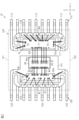
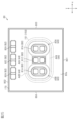
- the signal transmission device 10 is a semiconductor device in which multiple semiconductor chips are packaged together, and is mounted on a circuit board provided in the inverter device 500, for example. Note that each switching element 501, 502 is mounted on a mounting board separate from the circuit board. A cooler is attached to this mounting board.
- the package format of the signal transmission device 10 is an SO (Small Outline) type, and in this embodiment, it is an SOP (Small Outline Package).
- the low-voltage circuit chip 60, the high-voltage circuit chip 70, and the transformer chip 80 are, for example, semiconductor chips.
- the low-voltage circuit chip 60 is mounted on a low-voltage lead frame 100.
- the high-voltage circuit chip 70 is mounted on a high-voltage lead frame 110.
- the molded resin 120 seals a part of each lead frame 100, 110 and each chip 60, 70, 80.
- the transformer chip 80 and the molded resin 120 correspond to an "insulation module" that insulates the low-voltage circuit 20 and the high-voltage circuit 30.
- the molded resin 120 is shown by a two-dot chain line for the convenience of explaining the internal structure of the signal transmission device 10.
- the package format of the signal transmission device 10 can be changed arbitrarily.
- the molded resin 120 is made of a material having electrical insulation properties. This resin is, for example, a resin containing black epoxy resin.
- the molded resin 120 is formed in a rectangular plate shape with the z direction as the thickness direction.
- the molded resin 120 has four resin side surfaces 121 to 124. More specifically, the molded resin 120 has resin side surfaces 121 and 122 as both end faces in the x direction, and resin side surfaces 123 and 124 as both end faces in the y direction.
- the x direction and the y direction are directions perpendicular to the z direction.
- the x direction and the y direction are perpendicular to each other.
- the x direction corresponds to the "first direction”.
- the y direction corresponds to the "second direction”.
- a planar view means a view from the z direction.
- the low-voltage lead frame 100 and the high-voltage lead frame 110 are each a conductor, and in this embodiment are made of a material containing Cu (copper), Fe (iron), etc. Each lead frame 100, 110 is provided across the inside and outside of the molded resin 120.
- the low-voltage lead frame 100 has a low-voltage die pad 101 disposed within the molded resin 120, and a number of low-voltage leads 102 disposed across the inside and outside of the molded resin 120.
- Each low-voltage lead 102 constitutes an external terminal that electrically connects to an external electronic device such as a control circuit 503 (see FIG. 1).
- both the low-voltage circuit chip 60 and the transformer chip 80 are mounted on the low-voltage die pad 101.
- the low-voltage die pad 101 is positioned so that its center in the y direction is closer to the resin side surface 123 than the center in the y direction of the molded resin 120.
- the low-voltage die pad 101 is not exposed from the molded resin 120.
- the shape of the low-voltage die pad 101 is rectangular with the long side direction in the x direction and the short side direction in the y direction.
- the multiple low-voltage leads 102 are arranged spaced apart from each other in the x direction. Of the multiple low-voltage leads 102, each of the low-voltage leads 102 arranged at both ends in the x direction is integrated with the low-voltage die pad 101. A portion of each low-voltage lead 102 protrudes outward from the resin side surface 123 of the molded resin 120.
- the high-voltage lead frame 110 has a high-voltage die pad 111 arranged within the molded resin 120, and a number of high-voltage leads 112 arranged across the inside and outside of the molded resin 120.
- Each high-voltage lead 112 constitutes an external terminal that electrically connects to an external electronic device, such as the gate of a switching element 501 (see FIG. 1).
- the high-voltage die pad 111 is mounted with a high-voltage circuit chip 70.
- the high-voltage die pad 111 is disposed closer to the resin side surface 124 in the y direction than the low-voltage die pad 101.
- the high-voltage die pad 111 is not exposed from the molded resin 120.
- the shape of the high-voltage die pad 111 is rectangular with the long side direction being in the x direction and the short side direction being in the y direction.
- the low-voltage die pad 101 and the high-voltage die pad 111 are arranged apart from each other in the y direction. Therefore, the y direction can also be said to be the arrangement direction of both the die pads 101, 101.
- the dimensions in the y direction of the low-voltage die pad 101 and the high-voltage die pad 111 are set according to the size and number of semiconductor chips to be mounted.
- the low-voltage circuit chip 60 and the transformer chip 80 are mounted on the low-voltage die pad 101
- the high-voltage circuit chip 70 is mounted on the high-voltage die pad 111.
- the dimension in the y direction of the low-voltage die pad 101 is larger than the dimension in the y direction of the high-voltage die pad 111.
- the multiple high-voltage leads 112 are arranged spaced apart from each other in the x direction. Of the multiple high-voltage leads 112, a pair of high-voltage leads 112 are integrated with the high-voltage die pad 111. A portion of each high-voltage lead 112 protrudes outward from the resin side surface 124 of the molded resin 120.
- the number of high-voltage leads 112 is the same as the number of low-voltage leads 102.
- the multiple low-voltage leads 102 and the multiple high-voltage leads 112 are arranged in a direction (x direction) perpendicular to the arrangement direction (y direction) of the low-voltage die pads 101 and high-voltage die pads 111. Note that the number of high-voltage leads 112 and the number of low-voltage leads 102 can each be changed arbitrarily.
- the low-voltage die pad 101 is supported by a pair of low-voltage leads 102 that are integrated with the low-voltage die pad 101.
- the high-voltage die pad 111 is supported by a pair of high-voltage leads 112 that are integrated with the high-voltage die pad 111. Therefore, each die pad 101, 101 does not have a hanging lead exposed from the resin side surface 121, 122. This allows for a large insulation distance between the low-voltage lead frame 100 and the high-voltage lead frame 110.
- the low-voltage circuit chip 60, the high-voltage circuit chip 70, and the transformer chip 80 are arranged at a distance from each other in the y direction. In the y direction, the low-voltage circuit chip 60, the transformer chip 80, and the high-voltage circuit chip 70 are arranged in this order from the low-voltage lead 102 to the high-voltage lead 112.
- the low-voltage circuit chip 60 includes the low-voltage circuit 20 shown in FIG. 1.
- the low-voltage circuit chip 60 has a rectangular shape having short and long sides.
- the low-voltage circuit chip 60 is mounted on the low-voltage die pad 101 so that the long sides run along the x direction and the short sides run along the y direction.
- the low-voltage circuit chip 60 has a chip main surface 60s and a chip back surface 60r that face opposite each other in the z direction.
- the chip back surface 60r of the low-voltage circuit chip 60 is bonded to the low-voltage die pad 101 by a conductive bonding material SD.
- the conductive bonding material SD may be solder, Ag (silver) paste, or the like.
- a plurality of first electrode pads 61, a plurality of second electrode pads 62, and a plurality of third electrode pads 63 are formed on the chip main surface 60s of the low-voltage circuit chip 60. Each of the electrode pads 61 to 63 is electrically connected to the low-voltage circuit 20.
- the multiple first electrode pads 61 are arranged on the chip main surface 60s closer to the low voltage lead 102 than the center of the chip main surface 60s in the y direction.
- the multiple first electrode pads 61 are arranged in the x direction.
- the multiple second electrode pads 62 are arranged at the end of the chip main surface 60s in the y direction that is closer to the transformer chip 80.
- the multiple second electrode pads 62 are arranged in the x direction.
- the multiple third electrode pads 63 are arranged at both ends of the chip main surface 60s in the x direction.
- the high-voltage circuit chip 70 includes the high-voltage circuit 30 shown in FIG. 1.
- the high-voltage circuit chip 70 has a rectangular shape with short and long sides.
- the high-voltage circuit chip 70 is mounted on the high-voltage die pad 111 so that the long sides run along the x direction and the short sides run along the y direction.
- the high-voltage circuit chip 70 has a chip main surface 70s and a chip back surface 70r that face opposite each other in the z direction.
- the chip back surface 70r of the high-voltage circuit chip 70 is joined to the high-voltage die pad 111 by a conductive bonding material SD.
- a plurality of first electrode pads 71, a plurality of second electrode pads 72, and a plurality of third electrode pads 73 are formed on the chip main surface 70s of the high-voltage circuit chip 70. Each of the electrode pads 71 to 73 is electrically connected to the high-voltage circuit 30.
- the multiple first electrode pads 71 are arranged at the ends of the chip main surface 70s in the y direction that are closer to the transformer chip 80.
- the multiple first electrode pads 71 are arranged in the x direction.
- the multiple second electrode pads 72 are arranged at the ends of the chip main surface 70s in the y direction that are farther from the transformer chip 80. In other words, the multiple second electrode pads 72 are arranged at the ends of the chip main surface 70s in the y direction that are closer to the high voltage lead 112.
- the multiple second electrode pads 72 are arranged in the x direction.
- the multiple third electrode pads 73 are arranged at both ends of the chip main surface 70s in the x direction.
- the transformer chip 80 includes the transformer 40 (40A, 40B) shown in FIG. 1.
- the shape of the transformer chip 80 in plan view is a rectangle having short and long sides.
- the transformer chip 80 is mounted on the low-voltage die pad 101 so that, in plan view, the long side is aligned along the x direction and the short side is aligned along the y direction.
- the transformer chip 80 is disposed next to the low-voltage circuit chip 60 in the y direction.
- the transformer chip 80 is disposed closer to the high-voltage circuit chip 70 than the low-voltage circuit chip 60. In other words, the transformer chip 80 is disposed between the low-voltage circuit chip 60 and the high-voltage circuit chip 70 in the y direction.
- the transformer chip 80 has a chip main surface 80s and a chip back surface 80r that face opposite each other in the z direction.
- the chip back surface 80r of the transformer chip 80 is bonded to the low-voltage die pad 101 by a conductive bonding material SD.
- a plurality of first electrode pads 81 and a plurality of second electrode pads 82 are formed on a chip main surface 80s of the transformer chip 80.
- the second electrode pads 82 are arranged, for example, at one of both ends in the y direction of the chip main surface 80s, which is closer to the low-voltage circuit chip 60.
- the second electrode pads 82 are arranged in the x direction.
- the first electrode pads 81 are arranged, for example, near the center in the y direction of the chip main surface 80s.
- the first electrode pads 81 are arranged in the x direction.
- the distance between the high-voltage circuit chip 70 and the transformer chip 80 is greater than the distance between the low-voltage circuit chip 60 and the transformer chip 80.
- a number of wires W1 to W4 are connected to each of the low-voltage circuit chip 60, the transformer chip 80, and the high-voltage circuit chip 70.
- Each of the wires W1 to W4 is a bonding wire formed by a wire bonding device, and is made of a conductor containing, for example, Au (gold), Al (aluminum), Cu, etc.
- the low-voltage circuit chip 60 is electrically connected to the low-voltage lead frame 100 by the wire W1. More specifically, the low-voltage circuit chip 60's first electrode pads 61 and third electrode pads 63 are connected to the low-voltage leads 102 by the wire W1. The low-voltage circuit chip 60's third electrode pads 63 are connected to a pair of low-voltage leads 102 that are integrated with the low-voltage die pad 101 by the wire W1. This electrically connects the low-voltage circuit 20 to the low-voltage leads 102 (the external electrodes of the signal transmission device 10 that are electrically connected to the control circuit 503).
- the pair of low-voltage leads 102 that are integrated with the low-voltage die pad 101 constitute ground terminals, and the low-voltage circuit 20 and the low-voltage die pad 101 are electrically connected by the wire W1. Therefore, the low-voltage die pad 101 has the same potential as the ground GND1 of the low-voltage circuit 20.
- the high-voltage circuit chip 70 and the multiple high-voltage leads 112 of the high-voltage lead frame 110 are each electrically connected by a wire W4. More specifically, the multiple second electrode pads 72 and multiple third electrode pads 73 of the high-voltage circuit chip 70 are connected to the high-voltage leads 112 by the wire W4. This electrically connects the high-voltage circuit 30 and the multiple high-voltage leads 112 (the external electrodes of the signal transmission device 10 that are electrically connected to the switching element 501, etc.).
- a pair of high-voltage leads 112 integrated with the high-voltage die pad 111 constitute a ground terminal, and the high-voltage circuit 30 and the high-voltage die pad 111 are electrically connected by the wire W4. Therefore, the high-voltage die pad 111 has the same potential as the ground GND2 of the high-voltage circuit 30.
- the transformer chip 80 is connected to the low-voltage circuit chip 60 by wire W2.
- the transformer chip 80 is also connected to the high-voltage circuit chip 70 by wire W3. More specifically, the multiple second electrode pads 82 of the transformer chip 80 are connected to the multiple second electrode pads 62 of the low-voltage circuit chip 60 by wire W2.
- the multiple first electrode pads 81 of the transformer chip 80 are connected to the multiple first electrode pads 71 of the high-voltage circuit chip 70 by wire W3.
- both the second coils 42 of the transformers 40A and 40B are electrically connected to the ground GND1 of the low-voltage circuit 20 via the wire W2 and the low-voltage circuit chip 60, etc.
- the first coils 41 of the transformers 40A and 40B are electrically connected to the ground GND2 of the high-voltage circuit 30 via the wire W3 and the high-voltage circuit chip 70, etc.
- Transformer chip configuration An example of the configuration of the transformer chip 80 will be described with reference to FIGS. In the following description, the direction from the chip back surface 80r to the chip main surface 80s of the transformer chip 80 shown in Figures 8 and 9 is referred to as "upward,” and the direction from the chip main surface 80s to the chip back surface 80r is referred to as "downward.”
- FIG. 4 is a perspective view showing the external appearance of the transformer chip 80.
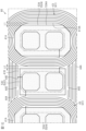
- FIG. Fig. 5 is a plan view of the transformer chip 80.
- the passivation film 160 is indicated by a two-dot chain line, and the transformers 40A and 40B and a floating dummy wiring 150 (described later) are indicated by dashed lines.
- FIG. 6 is a cross-sectional view of the transformer chip 80 taken on the xy plane at the z-direction position of the second coil 42, showing the connection relationship of the second coil 42.
- FIG. 7 is a cross-sectional view of the transformer chip 80 taken on the xy plane at the z-direction position of the first coil 41, showing the connection relationship of the first coil 41. Note that hatching has been omitted in FIGS. 6 and 7 for the sake of convenience.
- FIG. 8 is a cross-sectional view of the transformer chip 80 taken along line 8-8 in FIG. 5, showing the cross-sectional structures of the first coil 41, the floating dummy wiring 150, and the first pad 81A.
- FIG. 9 is a cross-sectional view of the transformer chip 80 taken along line 9-9 in FIG. 5, showing the cross-sectional structures of the outer dummy wiring 44, the floating dummy wiring 150, the second pad 81C, and the fourth pad 82C. For convenience, hatching has been omitted for some components in FIGS. 8 and 9.
- FIG. 10 is a schematic plan view of an enlarged portion of the transformer chip 80, showing the first pad 81A and the second pad 81C, the first coil 41, and the floating dummy wiring 150.
- FIG. 11 is a cross-sectional view of the transformer chip 80 taken along line 11-11 in FIG. 10, showing the cross-sectional structures of the first coil 41, the first pad 81A, and the second pad 81C.
- the transformer chip 80 of this embodiment includes two pairs of transformers 40A, 40B. More specifically, the transformer chip 80 is a semiconductor chip that integrates the two pairs of transformers 40A, 40B into a single chip. In other words, the transformer chip 80 is provided separately from the low-voltage circuit chip 60 and the high-voltage circuit chip 70 (both see FIG. 2).
- the transformers 40A and 40B are arranged near the center of the chip main surface 80s in the y direction in a plan view.
- the multiple first electrode pads 81 and the transformers 40A and 40B are arranged in positions that do not overlap each other in a plan view.
- Each electrode pad 81 and 82 is electrically connected to the transformers 40A and 40B.
- the first electrode pad 81 includes a first pad 81A arranged in the inner region 41A of the transformers 40A and 40B, and a second pad 81C arranged outside the transformers 40A and 40B.
- the first pad 81A is electrically connected to the transformers 40A and 40B, respectively.
- the second pad 81C is arranged between the transformers 40A and 40B.
- the second pad 81C is electrically connected to the transformers 40A and 40B. It can be said that the second pad 81C is provided as a common pad for the two transformers 40A and 40B.
- the first pad 81A has a shape in which the length in the y direction perpendicular to the x direction is greater than the length in the x direction in which the first electrode pads 81 are arranged.
- the shape of the first pad 81A is an ellipse that is longer in the y direction.
- the second pad 81C has a shape in which the length in the y direction perpendicular to the x direction is greater than the length in the x direction in which the first electrode pads 81 are arranged.
- the shape of the second pad 81C is a rectangle that is longer in the y direction.
- the multiple second electrode pads 82 are arranged at positions aligned with the two transformers 40A and the two transformers 40B in the x direction, and between the transformers 40A and 40B in the x direction.
- the multiple second electrode pads 82 are arranged closer to the chip side surface 802 in the y direction than the transformers 40A and 40B.
- the multiple second electrode pads 82 are arranged between the transformers 40A and 40B and the chip side surface 802 in the y direction.
- the multiple second electrode pads 82 can also be said to be arranged closer to the low-voltage lead 102 (see FIG. 2) than the transformers 40A and 40B.
- the second electrode pads 82 have a shape that is long in the x direction in which the second electrode pads 82 are arranged. In one example, the shape of the second electrode pads 82 is a rectangle that is long in the x direction.
- the second electrode pads 82 include a third pad 82A corresponding to the first pad 81A of the first electrode pad 81, and a fourth pad 82C corresponding to the second pad 81C of the first electrode pad 81.
- the third pad 82A is electrically connected to the transformers 40A and 40B, respectively.
- the fourth pad 82C is electrically connected to the transformer 40A and the transformer 40B. It can be said that the fourth pad 82C is provided as a common pad for the two transformers 40A and 40B.
- the third pad 82A is arranged at a position overlapping with the transformers 40A and 40B when viewed from the y direction.
- the fourth pad 82C is arranged at a position overlapping with the portion between the transformers 40A and 40B in the x direction when viewed from the y direction. Therefore, the multiple second electrode pads 82 (82A, 82C) are aligned with each other in the y direction and spaced apart from each other in the x direction.
- transformer 40B Each pair of transformers 40A, 40B have the same configuration. Furthermore, transformer 40B is configured in the same manner as transformer 40A. Therefore, the detailed structure of transformer 40A will be described, and a description of transformer 40B will be omitted.
- the transformer chip 80 has four chip side surfaces 801, 802, 803, and 804 that are perpendicular to both the chip main surface 80s and the chip back surface 80r.
- the chip side surfaces 801 to 804 are provided between the chip main surface 80s and the chip back surface 80r in the z direction.
- the chip side surfaces 801 and 802 form both end faces of the transformer chip 80 in the y direction, and the chip side surfaces 803 and 804 form both end faces of the transformer chip 80 in the x direction.
- the chip side surfaces 801 and 802 form the long sides of the transformer chip 80, and the chip side surfaces 803 and 804 form the short sides of the transformer chip 80.
- the chip side surface 801 is closer to the high-voltage circuit chip 70 (see FIG. 2) than the chip side surface 802, and the chip side surface 802 is closer to the low-voltage circuit chip 60 (see FIG. 2) than the chip side surface 801.
- the transformer chip 80 has a substrate 83 and an insulating layer 84 formed on the substrate 83.
- the substrate 83 is, for example, a semiconductor substrate.
- the substrate 83 is a substrate formed from a material containing Si (silicon).
- Examples of the Si substrate used for the substrate 83 include a semiconductor substrate made of a single crystal intrinsic semiconductor material, a p-type semiconductor substrate containing an acceptor-type impurity, and an n-type semiconductor substrate containing a donor-type impurity.
- the substrate 83 may be a semiconductor substrate using a wide band gap semiconductor or a compound semiconductor. Alternatively, the substrate 83 may be an insulating substrate made of a material containing glass instead of a semiconductor substrate.
- the wide band gap semiconductor is a semiconductor substrate having a band gap of 2.0 eV or more.
- the wide band gap semiconductor may be SiC (silicon carbide), GaN (gallium nitride), Ga 2 O 3 (gallium oxide), or the like.
- the compound semiconductor may be a III-V group compound semiconductor.
- the compound semiconductor may include at least one of AlN (aluminum nitride), InN (indium nitride), GaN, and GaAs (gallium arsenide).
- the substrate 83 has a substrate main surface 83s and a substrate back surface 83r that face opposite each other in the z direction.
- the substrate back surface 83r constitutes the chip back surface 80r of the transformer chip 80.
- the insulating layer 84 of this embodiment has multiple insulating films 85 stacked in the z direction from the substrate main surface 83s of the substrate 83.
- the z direction can also be said to be the thickness direction of the insulating layer 84.
- the z direction can also be said to be the stacking direction of the insulating films 85.
- the insulating layer 84 is formed on the substrate main surface 83s of the substrate 83.
- the insulating layer 84 includes an upper surface 84s and a lower surface 84r facing the opposite side to the upper surface 84s.
- the insulating film 85 has a first insulating film 85A and a second insulating film 85B formed on the first insulating film 85A.
- the first insulating film 85A is a thin film, for example, an etching stopper layer.
- the first insulating film 85A is formed of a material including SiN (silicon nitride), SiC, SiCN (nitrogen-added silicon carbide), or the like.
- the first insulating film 85A is formed of a material including SiN.
- the second insulating film 85B is, for example, an interlayer insulating film.
- the second insulating film 85B is formed of a material including SiO 2 (silicon oxide).
- the thickness of the second insulating film 85B is thicker than the thickness of the first insulating film 85A.
- the thickness of the first insulating film 85A may be 100 nm or more and less than 1000 nm.
- the thickness of the second insulating film 85B may be 1000 nm or more and 3000 nm or less. In this embodiment, the thickness of the first insulating film 85A is, for example, about 300 nm, and the thickness of the second insulating film 85B is, for example, about 2000 nm.
- the bottom insulating film 85L in contact with the substrate main surface 83s of the substrate 83 and the top insulating film 85U are both composed of the second insulating film 85B.
- the thicknesses of both the bottom insulating film 85L and the top insulating film 85U are thinner than the other insulating films 85.
- the thicknesses of both the bottom insulating film 85L and the top insulating film 85U are greater than or equal to the thickness of the first insulating film 85A and less than or equal to the thickness of the second insulating film 85B.
- the thickness of both the bottom insulating film 85L and the top insulating film 85U can be changed as desired.
- the thickness of both the bottom insulating film 85L and the top insulating film 85U may be thicker than the thickness of the second insulating film 85B, or may be greater than or equal to the thickness of the insulating film 85 formed by the first insulating film 85A and the second insulating film 85B.
- the second coil 42 of the transformers 40A and 40B is composed of the second coil wiring 46.
- the shape of the second coil wiring 46 is an elliptical spiral shape in a plan view.
- the second coil 42 is composed of a material including one or more appropriately selected from Ti (titanium), TiN (titanium nitride), Au, Ag, Cu, Al, and W (tungsten).
- An inner end wiring 57 is disposed inside the second coil wiring 46, and an outer end wiring 58 is disposed outside the second coil wiring 46.
- One end of the second coil wiring 46 is electrically connected to the inner end wiring 57, and the other end of the second coil wiring 46 is electrically connected to the outer end wiring 58.
- the inner end wiring 57 and the outer end wiring 58 are made of a material containing one or more appropriately selected from Ti, TiN, Au, Ag, Cu, Al, and W.
- the outer end wiring 58 is configured as a common end wiring for the second coils 42 of the transformers 40A and 40B. It is also possible to provide an outer end wiring for each of the second coils 42 of the transformers 40A and 40B.
- connection wiring 131A is made of a material containing one or more appropriately selected from Ti, TiN, Au, Ag, Cu, Al, and W.
- the connection wiring 131A has a first wiring portion 132A that extends in the z direction so as to penetrate a plurality of insulating films 85, and a second wiring portion 133A that extends in the y direction.
- the first wiring portion 132A is disposed at a position overlapping the third pad 82A in a plan view, and is connected to the third pad 82A.
- the first wiring portion 132A penetrates from the insulating film 85 below the uppermost insulating film 85U to the insulating film 85 two layers above the lowermost insulating film 85L among the multiple insulating films 85.
- the first wiring portion 132A has a flat wiring portion and multiple vias.
- the wiring portions are provided at the same positions as the insulating films 851 and 852 on which the coils 41 and 42 are provided.
- the vias are provided between the two wiring portions in the z direction, between the upper wiring portion and the third pad 82A, and between the lower wiring portion and the second wiring portion 133A.
- the second wiring portion 133A is provided closer to the substrate 83 than the first wiring portion 132A.
- the second wiring portion 133A is provided closer to the substrate 83 than the second coil 42.
- the second wiring portion 133A is provided in an insulating film 85 one layer above the lowest insulating film 85L among the multiple insulating films 85.
- the first end closer to the chip side surface 802 of the transformer chip 80 is provided at a position overlapping with the first wiring portion 132A in a planar view.
- the second wiring portion 133A is connected to the first wiring portion 132A.
- the second end opposite to the first end is provided at a position overlapping with the second coil 42 of the transformer 40A in a planar view.
- the second end is provided at a position overlapping with the inner end wiring 57 to which the second coil 42 of the transformer 40A is connected in a planar view.
- the second wiring portion 133A has multiple vias 134A that connect the second wiring portion 133A to the inner end wiring 57.
- connection wiring 131C is made of a material containing one or more appropriately selected from Ti, TiN, Au, Ag, Cu, Al, and W.
- connection wiring 131C has a first wiring portion 132C that extends in the z direction so as to penetrate a plurality of insulating films 85, and a second wiring portion 133C that extends in the y direction.
- the first wiring portion 132C is configured similarly to the first wiring portion 132A of the connection wiring 131A.
- the first wiring portion 132C is disposed at a position overlapping the fourth pad 82C in a plan view, and is connected to the fourth pad 82C.
- the first wiring portion 132C penetrates from the insulating film 85 below the uppermost insulating film 85U to the insulating film 85 two layers above the lowermost insulating film 85L among the multiple insulating films 85.
- the first wiring portion 132C has a flat wiring portion and multiple vias.
- the wiring portions are provided at the same positions as the insulating films 851 and 852 on which the coils 41 and 42 are provided.
- the vias are provided between the two wiring portions in the z direction, between the upper wiring portion and the third pad 82A, and between the lower wiring portion and the second wiring portion 133C.
- the second wiring portion 133C is provided closer to the substrate 83 than the first wiring portion 132C.
- the second wiring portion 133C is provided closer to the substrate 83 than the second coil 42.
- the second wiring portion 133C is provided in an insulating film 85 one layer above the lowest insulating film 85L among the multiple insulating films 85.
- the first end closer to the chip side surface 802 of the transformer chip 80 is provided at a position overlapping with the first wiring portion 132C in a planar view.
- the second wiring portion 133C is connected to the first wiring portion 132C.
- the second end opposite to the first end is provided at a position not overlapping with the second coil 42 of the transformer 40A in a planar view.
- the second end is provided at a position overlapping with the outer end wiring 58 to which the second coil 42 of the transformer 40A is connected in a planar view.
- the second wiring portion 133C has a plurality of vias 134C that connect the second wiring portion 133C and the outer end wiring 58.
- the second wiring portion 133C of the connection wiring 131C is electrically connected to the substrate 83 by vias 136 that penetrate the insulating film 85L of the lowest layer. Note that the vias 136 may be omitted.
- the first coil 41 of the transformers 40A and 40B includes a first coil wiring 43.
- the shape of the first coil wiring 43 is an elliptical spiral shape in a plan view.
- the first coil 41 is made of a material including one or more appropriately selected from Ti, TiN, Au, Ag, Cu, Al, and W.
- a first pad 81A is disposed in the inner region 41A of the first coil wiring 43.
- a second pad 81C is disposed outside the first coil wiring 43.
- One end of the first coil wiring 43 is electrically connected to the first pad 81A, and the other end of the first coil wiring 43 is electrically connected to the second pad 81C.
- the first electrode pad 81 (first pad 81A and second pad 81C) is made of a material containing one or more appropriately selected from Ti, TiN, Au, Ag, Cu, Al, and W.
- the second pad 81C is configured as a common pad for the first coils 41 of the transformers 40A and 40B. Note that the second pad 81C may be provided for each of the first coils 41 of the transformers 40A and 40B.
- the first coil wiring 43 is formed in the same winding direction as the second coil wiring 46 shown in FIG. 6 when viewed in a plan view.
- the number of turns of the first coil wiring 43 is the same as the number of turns of the second coil wiring 46.
- the second coil 42 and the first coil 41 of the transformer 40A are arranged opposite each other in the z direction via an insulating film 85.
- the second coil 42 and the first coil 41 are arranged opposite each other in the z direction via a plurality of insulating films 85.
- the second coil 42 is configured as a conductive layer embedded in one insulating film 85. More specifically, the insulating film 851 in which the second coil 42 is embedded has a coil groove (second coil groove) 141 that penetrates both the first insulating film 85A and the second insulating film 85B in the z direction. The conductive layer that constitutes the second coil 42 is embedded in the coil groove 141 of the insulating film 851. The insulating film 851 in which the second coil 42 is embedded is covered by the insulating film 85 that is adjacent to the insulating film 851 in the z direction. As a result, it can be said that the second coil 42 is embedded in the insulating film 85.
- the first coil 41 is configured as a conductive layer embedded in one insulating film 85. More specifically, the insulating film 852 in which the first coil 41 is embedded has a coil groove (first coil groove) 142 that penetrates both the first insulating film 85A and the second insulating film 85B in the z direction. The conductive layer that constitutes the first coil 41 is embedded in the coil groove 142 of the insulating film 852. The insulating film 852 in which the first coil 41 is embedded is covered by the insulating film 85 that is adjacent to the insulating film 852 in the z direction. As a result, it can be said that the first coil 41 is embedded in the insulating film 85.
- the first coil 41 is located farther from the substrate 83 than the second coil 42.
- the first coil 41 can be said to be located higher than the second coil 42.
- the second coil 42 can be said to be disposed closer to the substrate 83 than the first coil 41.
- the distance between the second coil 42 and the first coil 41 in the z direction is greater than the distance between the second coil 42 and the substrate main surface 83s of the substrate 83.
- the first pad 81A includes a base wiring 51A and a pad wiring 52A electrically connected to the base wiring 51A.
- the base wiring 51A is disposed at the same position as the first coil wiring 43 in the z direction. That is, the base wiring 51A is formed in the insulating film 852 in which the first coil 41 is embedded.
- the base wiring 51A is formed in a through hole that penetrates the insulating film 852 in the z direction.
- the pad wiring 52A is formed on the top insulating film 85U.
- the pad wiring 52A is electrically connected to the base wiring 51A by a via 54A that penetrates the insulating film 85U.
- the second pad 81C includes a base wiring 51C and a pad wiring 52C electrically connected to the base wiring 51C.
- the base wiring 51C is disposed in the same position in the z direction as the first coil wiring 43 (see FIG. 8). That is, the base wiring 51C is formed in the insulating film 852 in which the first coil 41 and the base wiring 51A of the first pad 81A shown in FIG. 8 are embedded.
- the base wiring 51C is formed in a through hole penetrating the insulating film 852 in the z direction.
- the pad wiring 52C is formed on the top insulating film 85U.
- the pad wiring 52C is electrically connected to the base wiring 51C by a via 54C penetrating the insulating film 85U.
- the third pad 82A includes a base wiring 91A and a pad wiring 92A electrically connected to the base wiring 91A.
- the base wiring 91A is disposed in the same position in the z direction as the first coil wiring 43 and the base wiring 51A of the first pad 81A. That is, the base wiring 91A is formed in the insulating film 852 in which the first coil 41 is embedded.
- the base wiring 91A is formed in a through hole that penetrates the insulating film 852 in the z direction.
- the pad wiring 92A is formed on the top insulating film 85U.
- the pad wiring 92A is electrically connected to the base wiring 91A by a via 94A that penetrates the insulating film 85U.
- the fourth pad 82C includes a base wiring 91C and a pad wiring 92C electrically connected to the base wiring 91C.
- the base wiring 91C is disposed in the same position in the z direction as the first coil wiring 43 (see FIG. 8). That is, the base wiring 91C is formed in the insulating film 852 in which the first coil 41 shown in FIG. 8 is embedded.
- the base wiring 91C is formed in a through hole that penetrates the insulating film 852 in the z direction.
- the pad wiring 92C is formed on the top insulating film 85U.
- the pad wiring 92C is electrically connected to the base wiring 91C by a via 94C that penetrates the insulating film 85U.
- the first coil 41 of this embodiment includes an outer dummy wiring 44.
- the outer dummy wiring 44 is a wiring pattern formed so that no current flows through the first coil wiring 43 of the first coil 41.
- the outer dummy wiring 44 includes a first dummy wiring 44A, a second dummy wiring 44B, and a third dummy wiring 44C.
- the first dummy wiring 44A and the second dummy wiring 44B are formed from a material containing one or more appropriately selected from Ti, TiN, Au, Ag, Cu, Al, and W.
- the first dummy wiring 44A is provided in a region between the first coil wiring 43 of the transformer 40A and the first coil wiring 43 of the transformer 40B in the x direction in a plan view, in which the second pad 81C is located.
- the third dummy wiring 44C is provided in a region between the first coil wiring 43 of the transformer 40A and the first coil wiring 43 of the transformer 40B in the x direction, in which the second pad 81C is not located, in a plan view.
- the first dummy wiring 44A and the third dummy wiring 44C are formed in a pattern different from that of the first coil wiring 43.
- the first dummy wiring 44A and the third dummy wiring 44C are composed of a plurality of wirings.
- the wiring width and wiring spacing of the first dummy wiring 44A and the third dummy wiring 44C composed of a plurality of wirings are equal to the wiring width and wiring spacing of the first coil wiring 43, in one example.
- the density (wiring density) of the first dummy wiring 44A and the third dummy wiring 44C is equal to the density (wiring density) of the first coil wiring 43.
- the density of the first dummy wiring 44A and the third dummy wiring 44C may be different from the density of the first coil wiring 43.
- the density of the first dummy wiring 44A and the density of the third dummy wiring 44C may be different from each other.
- the first dummy wiring 44A and the third dummy wiring 44C have, in one example, a first slit 44D formed along the y direction. Due to this first slit 44D, the first dummy wiring 44A is formed in an open ring shape. The first slit 44D suppresses the formation of a current loop in the first dummy wiring 44A.
- the first dummy wiring 44A and the third dummy wiring 44C are electrically connected to the second pad 81C of the first electrode pad 81.
- the first dummy wiring 44A includes a first connection portion 44E electrically connected to the second pad 81C.
- the position of the first connection portion 44E is arbitrary. Note that the first dummy wiring 44A only needs to be electrically connected to one of the second pads 81C. In this way, the first dummy wiring 44A has the same potential as the first coil 41. For this reason, as the second reference potential of the first coil 41 changes, the voltage of the first dummy wiring 44A may sometimes become higher than the second coil 42, similar to the first coil 41.
- the first dummy wiring 44A is positioned in the z direction in a position that is aligned with the first coil 41. In other words, the first dummy wiring 44A is positioned farther away from the substrate 83 than the second coil 42. In other words, it can be said that the floating dummy wiring 150 is provided around the coil of the transformer 40A, 40B that is closer to the chip main surface 80s of the transformer chip 80.
- the first dummy wiring 44A By making the first dummy wiring 44A have the same voltage as the first coil 41, the voltage drop between the first coil 41 and the first dummy wiring 44A can be suppressed. Therefore, electric field concentration on the first coil 41 can be suppressed.
- the second dummy wiring 44B is formed to surround the first coil 41, the first dummy wiring 44A, and the third dummy wiring 44C in a plan view.
- the second dummy wiring 44B is electrically connected to the first dummy wiring 44A.
- the second dummy wiring 44B is electrically connected to the first coil 41.
- the second dummy wiring 44B includes a second connection portion 44F electrically connected to the first dummy wiring 44A. The position of the second connection portion 44F is arbitrary.
- the second dummy wiring 44B is composed of a plurality of wires surrounding the first coil 41 and the first dummy wiring 44A.
- the wiring width and wiring spacing of the second dummy wiring 44B composed of a plurality of wires are, in one example, equal to the wiring width and wiring spacing of the first coil wiring 43 of the first coil 41.
- the density (wiring density) of the second dummy wiring 44B is equal to the density (wiring density) of the first coil wiring 43.
- the density of the second dummy wiring 44B may be different from the density of the first coil wiring 43.
- the second dummy wiring 44B has a second slit 44G formed along the y direction. Due to this second slit 44G, the second dummy wiring 44B is formed in an open ring shape. The second slit 44G suppresses the formation of a current loop in the second dummy wiring 44B.
- the second dummy wiring 44B is arranged in a position aligned with the first coil 41 in the z direction.
- the second dummy wiring 44B is also arranged in a position aligned with the first coil 41 in the z direction.
- the second dummy wiring 44B is arranged in a position farther away from the substrate 83 than the second coil 42.
- the second dummy wiring 44B suppresses electric field concentration around the first coil 41.
- the floating dummy wiring 150 includes a first dummy pattern 151 and a second dummy pattern 152.
- the first dummy pattern 151 is formed of a material including one or more appropriately selected from Ti, TiN, Au, Ag, Cu, Al, and W.
- the floating dummy wiring 150 includes a second dummy pattern 152.
- the second dummy pattern 152 is formed of a material including one or more appropriately selected from Ti, TiN, Au, Ag, Cu, Al, and W.
- the first dummy pattern 151 is formed to surround the second dummy wiring 44B in a plan view.
- the first dummy pattern 151 is electrically independent from the first coil 41. In other words, the first dummy pattern 151 is not electrically connected to the first coil 41.
- the first dummy pattern 151 is composed of a plurality of wires. In one example, each of the plurality of wires is formed into a closed loop. In one example, the wiring width of the first dummy pattern 151 composed of a plurality of wires is equal to the wiring width of the first coil wiring 43 of the first coil 41. In one example, the wiring spacing of the first dummy pattern 151 is greater than the wiring spacing of the first coil wiring 43 of the first coil 41. In other words, the density (wiring density) of the first dummy pattern 151 is lower than the density (wiring density) of the first coil wiring 43. The density of the first dummy pattern 151 may be equal to the density of the first coil wiring 43.
- the first dummy pattern 151 is arranged in a position aligned with the first coil 41 in the z direction. Although not shown, the first dummy pattern 151 is also arranged in a position aligned with the first coil 41 in the z direction. In other words, the first dummy pattern 151 is arranged in a position farther from the substrate 83 than the second coil 42. As shown in FIG. 8 and FIG. 9, the outer dummy wiring 44 (44A, 44B) and the floating dummy wiring 150 (first dummy pattern 151) are arranged in positions aligned with each other in the z direction. The first dummy pattern 151 suppresses an increase in the electric field strength around the first coil 41.
- the second dummy pattern 152 is disposed between the first coil 41 and the second electrode pad 82 in a planar view.
- the second dummy pattern 152 extends along the x direction.
- the second dummy pattern 152 is formed along the second electrode pads 82 in a planar view.
- the second dummy pattern 152 may include a plurality of wirings.
- the second dummy pattern 152 is electrically independent from the first coil 41. In other words, the second dummy pattern 152 is not electrically connected to the first coil 41.
- the second dummy pattern 152 separates the second electrode pads 82 from the first coil 41.
- the transformer chip 80 includes a passivation film 160.
- the passivation film 160 is formed on the upper surface 84s of the insulating layer 84.
- the passivation film 160 is a film that protects the insulating layer 84.
- the passivation film 160 is a surface protective film for the transformer chip 80.
- the passivation film 160 is formed from a material that includes, for example, silicon oxide and silicon nitride. Examples of materials that include silicon nitride include SiN and SiCN.
- the passivation film 160 constitutes the chip main surface 80s of the transformer chip 80.
- the second electrode pad 82 and the first electrode pad 81 are covered by a passivation film 160.
- the passivation film 160 has openings that expose portions of the second electrode pad 82 and the first electrode pad 81.
- the second electrode pad 82 has an exposed surface for connecting the wire W2.
- the first electrode pad 81 has an exposed surface for connecting the wire W3.
- the transformer chip 80 includes a resin layer 170 formed on a passivation film 160.
- the resin layer 170 is formed of a material containing, for example, polyimide (PI).
- the resin layer 170 is separated into an inner resin layer and an outer resin layer by a separation groove 173. As shown in FIG. 4, in a plan view, the separation groove 173 is formed so as to surround the transformers 40A and 40B.
- the resin layer 170 includes a first resin opening 174 that exposes the second electrode pad 82, and a second resin opening 175 that exposes the first electrode pad 81.
- the first pad 81A is disposed in an inner region 41A surrounded by the first coil 41 in a plan view.
- the inner region 41A has an elliptical spiral shape due to the shape of the first coil 41.
- the pad wiring 52A of the first pad 81A has a first extension portion 53A extending toward the first coil 41. It can be said that the first pad 81A has a first extension portion 53A.
- the first extension portion 53A extends toward the first coil 41 from a position 5 ⁇ m inward from the inner end 41AA of the first coil 41.
- the first coil 41 is formed by the first coil wiring 43.
- the inner end 41AA of the first coil 41 is the inner end of the first coil wiring 43.
- the distance L1 between the tip 53AA of the first extension portion 53A and the inner end 41AA of the first coil 41 is 5 ⁇ m or less.
- the first extension portion 53A is formed in a ring shape. It is preferable that the distance L1 from the tip 53AA of the first extension portion 53A to the inner peripheral end 41AA be 5 ⁇ m or less around the entire circumference of the first extension portion 53A.
- the pad wiring 52C of the second pad 81C is located outside the first coil 41 and next to the first pad 81A.
- the second pad 81C is located in an outer region 41B surrounded by the first coil wiring 43 of the first coil 41 of the transformers 40A and 40B and the outer dummy wiring 44.
- the outer region 41B has a rectangular shape that is long in the y direction perpendicular to the x direction in plan view, relative to the x direction in which the first coils 41 are adjacent to each other.
- the pad wiring 52C of the second pad 81C has a second extension portion 53C extending toward the first coil 41. It can be said that the second pad 81C has the second extension portion 53C.
- the second extension portion 53C extends toward the first coil wiring 43 and the outer dummy wiring 44 from a position 5 ⁇ m away from the wiring portion of the first coil wiring 43 and the outer dummy wiring 44 that define the outer region 41B. In one example, the second extension portion 53C extends toward both the first coil wiring 43 and the outer dummy wiring 44. It is preferable that the distance L2 from the tip 53CA of the second extension portion 53C to the end of the first coil wiring 43 and the outer dummy wiring 44 is 5 ⁇ m or less.
- the second extension portion 53C is formed in a ring shape. It is preferable that the distance L2 from the tip 53CA of the second extension portion 53C to the first coil wiring 43 and the outer dummy wiring 44 is 5 ⁇ m or less over the entire circumference of the second extension portion 53C. Note that the distance between at least one of the first coil wiring 43 and the outer dummy wiring 44 and the second extension portion 53C does not have to be 5 ⁇ m or less in some parts in the circumferential direction of the second extension portion 53C.
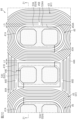
- FIG. 12 shows the results of a simulation of the electric field distribution and electric field strength in the vicinity of the first coil 41 (first coil wiring 43) and the first pad 81A in the transformer chip 80 of this embodiment.
- Fig. 13 shows the results of a simulation of the electric field distribution and electric field strength in the vicinity of the first coil 41X (first coil wiring 43) and the first pad 81A in the transformer chip 80X of the comparative example.
- the shading of the dots indicates the strength of the electric field strength. The higher the electric field strength, the darker the dots are.
- the two-dot chain lines indicate equipotential lines (electric field distribution).
- the distance L1X between the end of the first pad 81A and the inner peripheral end 41AA of the first coil 41X is greater than the distance L1 in the transformer chip 80 of this embodiment.
- the distance L1X in the comparative example is, for example, 20 ⁇ m.
- the equipotential lines wrap around from between the first coil 41X and the first pad 81A to the upper side of the first coil 41X. For this reason, it can be seen that electric field concentration occurs at the inner peripheral end of the first coil 41X. The dielectric strength voltage of the transformer chip 80X is reduced by this electric field concentration.
- the first pad 81A is arranged in the inner region 41A surrounded by the first coil 41 (first coil wiring 43) in a plan view.
- the first pad 81A has a first extension portion 53A that extends toward the first coil 41 from a position 5 ⁇ m inward from the inner end 41AA of the first coil 41. It can be seen that this first extension portion 53A prevents the equipotential lines from wrapping around the upper side of the first coil 41. Therefore, the electric field concentration at the inner end 41AA of the first coil 41 is alleviated. In other words, the first extension portion 53A of the first pad 81A suppresses the electric field concentration at the inner end 41AA of the first coil 41. This can improve the dielectric strength of the transformer chip 80.
- the second pad 81C is arranged in the outer region 41B surrounded by the first coil 41 (first coil wiring 43) and the outer dummy wiring 44 in a plan view.
- the second pad 81C has a second extension portion 53C extending toward the first coil 41.
- the second extension portion 53C extends toward the first coil wiring 43 and the outer dummy wiring 44 from a position 5 ⁇ m away from the wiring portion of the first coil wiring 43 and the outer dummy wiring 44 that define the outer region 41B. Therefore, similar to the first pad 81A, the second extension portion 53C of the second pad 81C can prevent the equipotential line from wrapping around the upper side of the first coil 41. Therefore, it is possible to alleviate the electric field concentration at the outer peripheral end of the first coil 41 that defines the outer region 41B. This can improve the dielectric strength of the transformer chip 80.
- first extension portion 53A that extends toward the first coil 41 from a position 5 ⁇ m inward from the inner end 41AA of the first coil 41. It can be seen that this first extension portion 53A prevents the equipotential lines from wrapping around to the upper side of the first coil 41. This reduces the electric field concentration at the inner end 41AA of the first coil 41. In other words, the first extension portion 53A of the first pad 81A suppresses the electric field concentration at the inner end 41AA of the first coil 41. This makes it possible to improve the dielectric strength of the transformer chip 80.
- the first coil 41 of the transformer chip 80 includes an outer dummy wiring 44 that surrounds the first coil wiring 43.
- the equipotential lines in the transformers 40A and 40B bypass the outer dummy wiring 44 that surrounds the first coil wiring 43. Therefore, electric field concentration at the outer peripheral end of the first coil wiring 43 is alleviated.
- the first coil 41 of the transformer chip 80 also includes a floating dummy wiring 150 (first dummy pattern 151) that surrounds the outer dummy wiring 44.
- first dummy pattern 151 the equipotential lines in the transformers 40A and 40B bypass the floating dummy wiring 150 that surrounds the outer dummy wiring 44. Therefore, the electric field concentration at the outer peripheral end of the outer dummy wiring 44, i.e., the outer peripheral end of the first coil 41, is alleviated.
- the first pad 81A is disposed in the inner region 41A surrounded by the first coil 41 (first coil wiring 43) in a plan view.
- the first pad 81A has a first extension portion 53A extending toward the first coil 41 from a position 5 ⁇ m away from the inner end 41AA of the first coil 41. It can be seen that the first extension portion 53A suppresses the equipotential lines from wrapping around the upper side of the first coil 41. Therefore, the electric field concentration at the inner end 41AA of the first coil 41 is alleviated. In other words, the first extension portion 53A of the first pad 81A suppresses the electric field concentration at the inner end 41AA of the first coil 41. This can improve the dielectric strength of the transformer chip 80.
- the second pad 81C is arranged in the outer region 41B surrounded by the first coil 41 (first coil wiring 43) and the outer dummy wiring 44 in a plan view.
- the second pad 81C has a second extension portion 53C extending toward the first coil 41.
- the second extension portion 53C extends toward the first coil wiring 43 and the outer dummy wiring 44 from a position 5 ⁇ m away from the wiring portion of the first coil wiring 43 and the outer dummy wiring 44 that divide the outer region 41B. Therefore, similar to the first pad 81A, the second extension portion 53C of the second pad 81C can prevent the equipotential lines from wrapping around the upper side of the first coil 41. Therefore, the electric field concentration at the outer peripheral end of the first coil 41 can be alleviated. This can improve the dielectric strength of the transformer chip 80.
- the first coil 41 of the transformer chip 80 includes an outer dummy wiring 44 that surrounds the first coil wiring 43.
- the equipotential lines in the transformers 40A and 40B bypass the outer dummy wiring 44 that surrounds the first coil wiring 43. This reduces electric field concentration at the outer circumferential end of the first coil wiring 43. This improves the dielectric strength of the transformer chip 80.
- the first coil 41 of the transformer chip 80 includes a floating dummy wiring 150 (first dummy pattern 151) surrounding the outer dummy wiring 44.
- the equipotential lines in the transformers 40A and 40B bypass the floating dummy wiring 150 surrounding the outer dummy wiring 44. Therefore, the electric field concentration at the outer peripheral end of the outer dummy wiring 44, i.e., the outer peripheral end of the first coil 41, is alleviated. Therefore, the dielectric strength of the transformer chip 80 can be improved.
- the multiple transformers 40A, 40B are arranged in a row along the x direction.
- the arrangement direction of these transformers 40A, 40B is the longitudinal direction of the transformer chip 80 in a plan view.
- the first coil 41 and the second coil 42 of each transformer 40A, 40B are formed in an elliptical shape that is long in the y direction in which the first electrode pad 81 and the second electrode pad 82 are aligned in a plan view.
- the y direction is the width direction (short direction) of the transformer chip 80.
- the transformer chip 80 includes the same number of transformers 40A, 40B, and the longitudinal length of the transformer chip 80 can be shortened compared to a transformer chip 80 that includes the same number of transformers 40A, 40B and that has each transformer 40A, 40B arranged in an elliptical shape that is long in the longitudinal direction. This makes it possible to suppress an increase in the longitudinal length of the transformer chip 80 when the number of transformers 40 is increased.
- the pad wiring 52A of the first pad 81A may be formed so as to cover a portion of the first coil wiring 43.
- the shape of the pad wiring 52A of the first pad 81A may be a rectangle whose length in the y direction is longer than its length in the x direction.
- the pad wiring 52A of the first pad 81A may be a polygonal shape (octagonal shape in Figure 16).
- the first pad 81A may be formed so as to cover the entire inner region 41A.
- the pad wiring 52C of the second pad 81C may be formed so as to cover a portion of the first coil wiring 43. Also, the pad wiring 52C of the second pad 81C may be formed so as to cover a portion of the outer dummy wiring 44. Furthermore, the pad wiring 52C of the second pad 81C may be formed so as to cover both a portion of the first coil wiring 43 and a portion of the outer dummy wiring 44, that is, so as to cover the entire outer region 41B.
- the shape of the pad wiring 52C of the second pad 81C may be any shape, such as an oval shape, a polygonal shape (octagonal shape), etc., like the first pad 81A.
- the size of the first pad 81A (pad wiring 52A) and the second pad 81C (pad wiring 52C) in a planar view may be changed as appropriate.
- the size of the second pad 81C is smaller than the size of the first pad 81A in a planar view.
- the size of the second pad 81C may be equal to the size of the first pad 81A, or may be larger than the size of the first pad 81A.
- a first pad 81A includes a base wiring 51A and a cap wiring 55A in contact with an upper surface 51As of the base wiring 51A.
- the base wiring 51A is disposed at the same position as the first coil wiring 43 of the first coil 41 in the z direction.
- the cap wiring 55A is formed on the upper surface of the insulating film 85U.
- the insulating film 85U has an opening 85U1 that exposes a portion of the upper surface 51As of the base wiring 51A.
- the cap wiring 55A is electrically connected to the base wiring 51A by contacting the upper surface 51As of the base wiring 51A within the opening 85U1 of the insulating film 85U.
- the cap wiring 55A is made of a material containing one or more appropriately selected from Cu, Al, Ni (nickel), Pd (palladium), and W.
- the cap wiring 55A protrudes beyond the base wiring 51A.
- the cap wiring 55A includes a first extension portion 56A that extends toward the first coil 41.
- the first extension portion 56A of the cap wiring 55A can reduce electric field concentration at the inner end 41AA of the first coil 41. This can improve the dielectric strength of the transformer chip 80.
- the transformer chip 80 shown in FIG. 18 includes a first pad 81A that includes a base wiring 51A and a cap wiring 55A, similar to the transformer chip shown in FIG. 17.
- the base wiring 51A protrudes beyond the cap wiring 55A.
- the base wiring 51A includes a first extension portion 57A that extends toward the first coil 41.
- the first extension portion 57A of the base wiring 51A can reduce electric field concentration at the inner end 41AA of the first coil 41. This can improve the dielectric strength of the transformer chip 80.
- the transformer chip 80 shown in FIG. 19 has a first pad 81A that includes a base wiring 51A and a cap wiring 55A, similar to the transformer chip shown in FIG. 17.
- both the base wiring 51A and the cap wiring 55A extend toward the first coil 41.
- both the base wiring 51A and the cap wiring 55A include the first extension portions 53A, 57A. This makes it possible to improve the dielectric strength of the transformer chip 80.
- the third pad 82A can include a base wiring 51C and a cap wiring in contact with the upper surface of the base wiring 51C, similar to the first pad 81A.
- the first pad 81A is described, but the second pad 81C shown in Fig. 9 can be configured in the same way as the first pad 81A.
- the third pad 82A is described, but the fourth pad 82C shown in Fig. 9 can be configured in the same way.
- the transformer chip 80 shown in Figures 20 and 21 includes an inner dummy wiring 45 arranged in the inner region 41A of the first coil 41.
- the inner dummy wiring 45 includes a plurality of wirings extending along the inside of the first coil wiring 43.
- the inner dummy wiring 45 is electrically connected to the first coil wiring 43.
- the first coil wiring 43 includes a connection portion 43A electrically connected to the first pad 81A.
- the inner dummy wiring 45 is electrically connected to the first coil wiring 43 by this connection portion 43A.
- the inner dummy wiring 45 has a slit 45B and is formed in an open ring shape.
- the first coil 41 can be said to include the inner dummy wiring 45.
- the inner end of the first coil 41 is the inner end 45AA of the inner dummy wiring 45.
- the pad wiring 52A of the first pad 81A has a first extension portion 53A extending toward the inner dummy wiring 45.
- the distance L3 between the tip 53AA of the first extension portion 53A and the inner end 45AA of the inner dummy wiring 45 is 5 ⁇ m or less.
- the transformer chip 80 of the modified example configured in this manner can reduce the electric field concentration at the inner end 41AA of the first coil 41, as in the transformer chip 80 of the above embodiment, and therefore can improve the dielectric strength of the transformer chip 80.
- the pad wiring 52A of the first pad 81A may be formed to cover part or all of the inner dummy wiring 45 in a plan view.
- the first coil wiring 43 of the first coil 41 is arranged instead of the inner dummy wiring 45 of the transformer chip 80 shown in Figs. 20 and 21. That is, the first coil wiring 43 of the first coil 41 is wound toward the base wiring 51A of the first pad 81A, so the number of turns of the first coil wiring 43 is large.
- the second coil wiring 46 of the second coil 42 is wound toward the inner end wiring 57, like the first coil wiring 43.
- the number of turns of the first coil wiring 43 and the second coil wiring 46 are the same. Note that the number of turns of the first coil wiring 43 and the second coil wiring 46 may be different.
- the pad wiring 52A of the first pad 81A has a first extension portion 53A extending toward the first coil wiring 43.
- the distance L4 between the tip 53AA of the first extension portion 53A and the inner end 41AA of the first coil wiring 43 is 5 ⁇ m or less.
- the transformer chip 80 configured in this manner can reduce electric field concentration at the inner end 41AA of the first coil 41, thereby improving the dielectric strength of the transformer chip 80.
- the number of transformers included in the transformer chip can be changed as needed.
- the transformer chip 80 shown in Fig. 24 includes four pairs of transformers 40A, 40B. In this way, in the transformer chip 80 including many transformers 40A, 40B, it is possible to suppress an increase in the length in the longitudinal direction (x direction). In other words, it is possible to increase the number of transformers included in the transformer chip 80 while suppressing an increase in the length in the longitudinal direction (x direction) of the transformer chip 80. In addition, it is possible to improve the dielectric strength of this transformer chip 80.
- 25 includes a pair of transformers 40 A and 40 B.
- this transformer chip 80 it is possible to improve the dielectric strength voltage.
- 26 includes one transformer 40.
- the second pad 81C is disposed in an outer region 41B surrounded by the first coil wiring 43 of the first coil 41 and the first dummy wiring 44A and the second dummy wiring 44B of the outer dummy wiring 44.
- This transformer chip 80 can improve the dielectric strength of the transformer chip 80, similar to the transformer chip 80 of the above embodiment.
- the configuration of the signal transmission device can be changed as appropriate.
- a configuration may be adopted in which a plurality of transformers are connected in series between the low voltage circuit 20 and the high voltage circuit 30 to transmit signals.
- FIG. 27 shows an example of a signal transmission device 10.
- This signal transmission device 10 includes two transformers 40, 240 between the low-voltage circuit 20 and the high-voltage circuit 30.
- the signal transmission device 10 includes two transformers 40A, 240A that transmit a set signal, and two transformers 40B, 240B that transmit a reset signal.
- the transformers 40A and 40B include a first coil 41 and a second coil 42.
- the transformers 240A and 240B include a first coil 241 and a second coil 242.
- the second coil 42 of the transformers 40A and 40B is electrically connected to the low-voltage circuit 20.
- the first coil 41 of the transformers 40A and 40B is electrically connected to the first coil 241 of the transformers 240A and 240B.
- the second coil 242 of the transformers 240A and 240B is electrically connected to the high-voltage circuit 30.
- FIG. 28 shows an example of a plan view illustrating the internal configuration of the signal transmission device 10 of FIG.
- the signal transmission device 10 includes a low-voltage circuit chip 60, a high-voltage circuit chip 70, a first transformer chip 80, and a second transformer chip 280.
- the low-voltage circuit chip 60, the high-voltage circuit chip 70, the first transformer chip 80, and the second transformer chip 280 are arranged apart from each other in the y direction. These chips 60, 70, 80, and 280 are arranged in the arrangement direction of the low-voltage die pad 101 and the high-voltage die pad 111.
- the low-voltage circuit chip 60, the first transformer chip 80, the second transformer chip 280, and the high-voltage circuit chip 70 are arranged in this order from the low-voltage lead 102 toward the high-voltage lead 112.
- the first transformer chip 80 and the second transformer chip 280 are arranged between the low-voltage circuit chip 60 and the high-voltage circuit chip 70.
- the low-voltage circuit chip 60 and the first transformer chip 80 are both mounted on the low-voltage die pad 101 of the low-voltage lead frame 100.
- the high-voltage circuit chip 70 and the second transformer chip 280 are mounted on the high-voltage die pad 111 of the high-voltage lead frame 110.
- the second electrode pads 82 of the first transformer chip 80 and the second transformer chip 280 are electrically connected to the high-voltage circuit chip 70 by wire W3.
- the first electrode pad 81 of the second transformer chip 280 is electrically connected to the first electrode pad 81 of the first transformer chip 80 by wire W5.
- Both the first transformer chip 80 and the second transformer chip 280 have the same configuration as the transformer chip 80 of the above embodiment. Therefore, the dielectric strength voltage is improved in both the first transformer chip 80 and the second transformer chip 280.
- the signal transmission device 10 has a dielectric strength voltage that corresponds to the dielectric strength voltage of each of the first transformer chip 80 and the second transformer chip 280 that are connected in series.
- a first layer is formed on a second layer is intended to mean that in some embodiments, the first layer may be in contact with the second layer and disposed directly on the second layer, while in other embodiments, the first layer may be disposed above the second layer without contacting the second layer.
- the term “on” does not exclude a structure in which another layer is formed between the first and second layers.
- the Z-axis direction used in this disclosure does not necessarily have to be the vertical direction, nor does it have to be perfectly aligned with the vertical direction.
- various structures according to this disclosure are not limited to the "up” and “down” in the Z-axis direction described in this specification being “up” and “down” in the vertical direction.
- the x-direction may be the vertical direction
- the y-direction may be the vertical direction.
- (Appendix 1) an insulating layer (84) including upper and lower surfaces facing in opposite directions in a thickness direction; a first coil (41) disposed in the insulating layer (84) toward the upper surface; a second coil (42) disposed in the insulating layer (84) toward the lower surface and facing the first coil (41); a first pad (81A) formed on the upper surface and electrically connected to the first coil (41); Including, The first pad (81A) is disposed in an inner region (41A) surrounded by the first coil (41) when viewed from the thickness direction, and includes a first extension portion (53A) extending toward the first coil (41) beyond a position 5 ⁇ m away from an inner peripheral end of the first coil (41). Transformer chip.
- the first extension portion (53A) is formed in an annular shape, and the distance from the tip to the inner peripheral end of the first extension portion (53A) is 5 ⁇ m or less over the entire circumference. 2.
- the first pad (81A) covers the entire inner region (41A). 3.
- the first coil (41) is It includes a spiral coil wiring through which a current flows, The inner circumferential end of the first coil (41) is the inner circumferential end of the coil wiring.
- the first coil (41) is A spiral coil wiring (43) through which a current flows; An inner dummy wiring (45) provided inside the coil wiring and configured so that the current does not flow; Including, The inner peripheral end of the first coil (41) is the inner peripheral end of the inner dummy wiring (45).
- a transformer chip according to any one of claims 1 to 3.
- the inner dummy wiring (45) is formed in an open ring shape having a slit (45B). 6.
- the density of the inner dummy wiring (45) is equal to the density of the coil wiring.
- FIG. 8 a second pad (81C) provided separately from the first pad (81A) and electrically connected to the first coil (41);
- the second pad (81C) is disposed outside the first coil (41) and adjacent to the first pad (81A), and includes a second extension portion (53C) extending toward the first coil (41) beyond a position 5 ⁇ m away from the outer circumferential end of the first coil (41) as viewed in the thickness direction.
- a transformer chip according to any one of claims 4 to 7.
- the first coil (41) includes an outer dummy wiring (44) that is arranged outside the coil wiring when viewed from the thickness direction and is configured so that the current does not flow
- the second pad (81C) is disposed in an outer region (41B) surrounded by the coil wiring and the outer dummy wiring (44),
- the second extension portion (53C) extends from a position 5 ⁇ m or more away from the wiring portions of the coil wiring and the outer dummy wiring (44) that define the outer region (41B) toward both the coil wiring and the outer dummy wiring (44).
- the second extension portion (53C) is formed in a ring shape, and the distance from the tip of the second extension portion (53C) to the ends of the coil wiring and the outer dummy wiring (44) is 5 ⁇ m or less over the entire circumference. 10.
- the second pad (81C) covers the entire outer region (41B).
- the second pad (81C) When viewed from the thickness direction, the second pad (81C) is arranged next to the first pad (81A) in the first direction, The second pad (81C) has a rectangular shape that is long in a second direction perpendicular to the first direction when viewed from the thickness direction.
- a transformer chip according to any one of claims 8 to 11.
- the inner region (41A) has an elliptical shape that is long in the second direction
- the first pad (81A) has an elliptical shape that is long in the second direction corresponding to the inner region (41A).
- the inner region (41A) has an elliptical shape that is long in the second direction, and the first pad (81A) has a rectangular shape that is long in the second direction corresponding to the inner region (41A). 13.
- the first pad (81A) is a base wiring (51A) provided at the same position as the first coil (41) in the thickness direction; a cap wiring (55A) in contact with an upper surface of the base wiring; It has the cap wiring protrudes beyond the base wiring, and the cap wiring includes the first extension portion (53A); A transformer chip according to any one of claims 1 to 14.
- the first pad (81A) is a base wiring (51A) provided at the same position as the first coil (41) in the thickness direction; a cap wiring (55A) in contact with an upper surface of the base wiring; It has The base wiring protrudes beyond the cap wiring, and the base wiring includes the first extension portion (53A).
- the first pad (81A) is a base wiring (51A) provided at the same position as the first coil (41) in the thickness direction; a cap wiring (55A) in contact with an upper surface of the base wiring; It has The cap wiring and the base wiring form the first extension portion (53A).
- the second coil (42) is formed in a spiral shape overlapping with the first coil (41) in the thickness direction. 18.
Landscapes
- Engineering & Computer Science (AREA)
- Power Engineering (AREA)
- Microelectronics & Electronic Packaging (AREA)
- Coils Or Transformers For Communication (AREA)
Priority Applications (2)
| Application Number | Priority Date | Filing Date | Title |
|---|---|---|---|
| JP2024576240A JPWO2024166718A1 (https=) | 2023-02-09 | 2024-01-29 | |
| US19/286,504 US20250357040A1 (en) | 2023-02-09 | 2025-07-31 | Transformer chip |
Applications Claiming Priority (2)
| Application Number | Priority Date | Filing Date | Title |
|---|---|---|---|
| JP2023-018609 | 2023-02-09 | ||
| JP2023018609 | 2023-02-09 |
Related Child Applications (1)
| Application Number | Title | Priority Date | Filing Date |
|---|---|---|---|
| US19/286,504 Continuation US20250357040A1 (en) | 2023-02-09 | 2025-07-31 | Transformer chip |
Publications (1)
| Publication Number | Publication Date |
|---|---|
| WO2024166718A1 true WO2024166718A1 (ja) | 2024-08-15 |
Family
ID=92262403
Family Applications (1)
| Application Number | Title | Priority Date | Filing Date |
|---|---|---|---|
| PCT/JP2024/002553 Ceased WO2024166718A1 (ja) | 2023-02-09 | 2024-01-29 | トランスチップ |
Country Status (3)
| Country | Link |
|---|---|
| US (1) | US20250357040A1 (https=) |
| JP (1) | JPWO2024166718A1 (https=) |
| WO (1) | WO2024166718A1 (https=) |
Citations (6)
| Publication number | Priority date | Publication date | Assignee | Title |
|---|---|---|---|---|
| JPH04363006A (ja) * | 1990-05-31 | 1992-12-15 | Toshiba Corp | 平面型磁気素子 |
| JP2015138874A (ja) * | 2014-01-22 | 2015-07-30 | ルネサスエレクトロニクス株式会社 | 半導体装置の製造方法 |
| JP2017216407A (ja) * | 2016-06-01 | 2017-12-07 | 住友電工プリントサーキット株式会社 | プリント配線板及びその製造方法 |
| WO2019074130A1 (ja) * | 2017-10-13 | 2019-04-18 | ローム株式会社 | 電子部品および電子部品モジュール |
| JP2021150839A (ja) * | 2020-03-19 | 2021-09-27 | 株式会社東芝 | アイソレータ |
| JP2021166295A (ja) * | 2019-03-08 | 2021-10-14 | ローム株式会社 | 絶縁通信部品およびモジュール |
-
2024
- 2024-01-29 JP JP2024576240A patent/JPWO2024166718A1/ja active Pending
- 2024-01-29 WO PCT/JP2024/002553 patent/WO2024166718A1/ja not_active Ceased
-
2025
- 2025-07-31 US US19/286,504 patent/US20250357040A1/en active Pending
Patent Citations (6)
| Publication number | Priority date | Publication date | Assignee | Title |
|---|---|---|---|---|
| JPH04363006A (ja) * | 1990-05-31 | 1992-12-15 | Toshiba Corp | 平面型磁気素子 |
| JP2015138874A (ja) * | 2014-01-22 | 2015-07-30 | ルネサスエレクトロニクス株式会社 | 半導体装置の製造方法 |
| JP2017216407A (ja) * | 2016-06-01 | 2017-12-07 | 住友電工プリントサーキット株式会社 | プリント配線板及びその製造方法 |
| WO2019074130A1 (ja) * | 2017-10-13 | 2019-04-18 | ローム株式会社 | 電子部品および電子部品モジュール |
| JP2021166295A (ja) * | 2019-03-08 | 2021-10-14 | ローム株式会社 | 絶縁通信部品およびモジュール |
| JP2021150839A (ja) * | 2020-03-19 | 2021-09-27 | 株式会社東芝 | アイソレータ |
Also Published As
| Publication number | Publication date |
|---|---|
| JPWO2024166718A1 (https=) | 2024-08-15 |
| US20250357040A1 (en) | 2025-11-20 |
Similar Documents
| Publication | Publication Date | Title |
|---|---|---|
| CN111919298B (zh) | 电子部件 | |
| JP7686394B2 (ja) | ゲートドライバ | |
| CN112400229B (zh) | 半导体器件 | |
| JP7824273B2 (ja) | 絶縁モジュールおよびゲートドライバ | |
| US12396264B2 (en) | Isolation transformer | |
| US12419112B2 (en) | Isolation transformer | |
| CN114762114A (zh) | 半导体装置 | |
| US20240029949A1 (en) | Insulating transformer | |
| WO2022210551A1 (ja) | アイソレータ、絶縁モジュールおよびゲートドライバ | |
| WO2024166718A1 (ja) | トランスチップ | |
| US20230387041A1 (en) | Semiconductor device and semiconductor module | |
| JP7803935B2 (ja) | 絶縁トランス | |
| WO2022210542A1 (ja) | 絶縁トランス、絶縁モジュールおよびゲートドライバ | |
| WO2024171760A1 (ja) | 絶縁チップおよび絶縁チップの製造方法 | |
| JP2024173373A (ja) | 信号伝達装置 | |
| JP2025014349A (ja) | 絶縁チップおよび信号伝達装置 | |
| US12615787B2 (en) | Isolator including electrically floating intermediate electrode portion | |
| US20250072012A1 (en) | Semiconductor device | |
| US20240421112A1 (en) | Semiconductor element and semiconductor device | |
| US20260120939A1 (en) | Transformer chip and signal transmission device | |
| US20260114337A1 (en) | Semiconductor device and insulating switch | |
| JP2025139228A (ja) | 半導体チップおよび半導体装置 | |
| JP2026069678A (ja) | 絶縁モジュールおよびゲートドライバ | |
| JP2024176796A (ja) | トランスチップおよび信号伝達装置 | |
| WO2025094846A1 (ja) | 半導体装置 |
Legal Events
| Date | Code | Title | Description |
|---|---|---|---|
| 121 | Ep: the epo has been informed by wipo that ep was designated in this application |
Ref document number: 24753162 Country of ref document: EP Kind code of ref document: A1 |
|
| ENP | Entry into the national phase |
Ref document number: 2024576240 Country of ref document: JP Kind code of ref document: A |
|
| WWE | Wipo information: entry into national phase |
Ref document number: 2024576240 Country of ref document: JP |
|
| NENP | Non-entry into the national phase |
Ref country code: DE |
|
| 122 | Ep: pct application non-entry in european phase |
Ref document number: 24753162 Country of ref document: EP Kind code of ref document: A1 |