WO2024166492A1 - 半導体装置 - Google Patents
半導体装置 Download PDFInfo
- Publication number
- WO2024166492A1 WO2024166492A1 PCT/JP2023/041808 JP2023041808W WO2024166492A1 WO 2024166492 A1 WO2024166492 A1 WO 2024166492A1 JP 2023041808 W JP2023041808 W JP 2023041808W WO 2024166492 A1 WO2024166492 A1 WO 2024166492A1
- Authority
- WO
- WIPO (PCT)
- Prior art keywords
- region
- contact
- mesa
- semiconductor device
- semiconductor substrate
- Prior art date
- Legal status (The legal status is an assumption and is not a legal conclusion. Google has not performed a legal analysis and makes no representation as to the accuracy of the status listed.)
- Ceased
Links
Images


Classifications
-
- H—ELECTRICITY
- H10—SEMICONDUCTOR DEVICES; ELECTRIC SOLID-STATE DEVICES NOT OTHERWISE PROVIDED FOR
- H10D—INORGANIC ELECTRIC SEMICONDUCTOR DEVICES
- H10D8/00—Diodes
- H10D8/422—PN diodes having the PN junctions in mesas
-
- H—ELECTRICITY
- H10—SEMICONDUCTOR DEVICES; ELECTRIC SOLID-STATE DEVICES NOT OTHERWISE PROVIDED FOR
- H10D—INORGANIC ELECTRIC SEMICONDUCTOR DEVICES
- H10D12/00—Bipolar devices controlled by the field effect, e.g. insulated-gate bipolar transistors [IGBT]
- H10D12/01—Manufacture or treatment
- H10D12/031—Manufacture or treatment of IGBTs
- H10D12/032—Manufacture or treatment of IGBTs of vertical IGBTs
- H10D12/035—Etching a recess in the emitter region
-
- H—ELECTRICITY
- H10—SEMICONDUCTOR DEVICES; ELECTRIC SOLID-STATE DEVICES NOT OTHERWISE PROVIDED FOR
- H10D—INORGANIC ELECTRIC SEMICONDUCTOR DEVICES
- H10D12/00—Bipolar devices controlled by the field effect, e.g. insulated-gate bipolar transistors [IGBT]
- H10D12/01—Manufacture or treatment
- H10D12/031—Manufacture or treatment of IGBTs
- H10D12/032—Manufacture or treatment of IGBTs of vertical IGBTs
- H10D12/038—Manufacture or treatment of IGBTs of vertical IGBTs having a recessed gate, e.g. trench-gate IGBTs
-
- H—ELECTRICITY
- H10—SEMICONDUCTOR DEVICES; ELECTRIC SOLID-STATE DEVICES NOT OTHERWISE PROVIDED FOR
- H10D—INORGANIC ELECTRIC SEMICONDUCTOR DEVICES
- H10D12/00—Bipolar devices controlled by the field effect, e.g. insulated-gate bipolar transistors [IGBT]
- H10D12/411—Insulated-gate bipolar transistors [IGBT]
- H10D12/417—Insulated-gate bipolar transistors [IGBT] having a drift region having a doping concentration that is higher at the collector side relative to other parts of the drift region
-
- H—ELECTRICITY
- H10—SEMICONDUCTOR DEVICES; ELECTRIC SOLID-STATE DEVICES NOT OTHERWISE PROVIDED FOR
- H10D—INORGANIC ELECTRIC SEMICONDUCTOR DEVICES
- H10D12/00—Bipolar devices controlled by the field effect, e.g. insulated-gate bipolar transistors [IGBT]
- H10D12/411—Insulated-gate bipolar transistors [IGBT]
- H10D12/418—Insulated-gate bipolar transistors [IGBT] having a drift region having a doping concentration that is higher at the emitter side relative to other parts of the drift region
-
- H—ELECTRICITY
- H10—SEMICONDUCTOR DEVICES; ELECTRIC SOLID-STATE DEVICES NOT OTHERWISE PROVIDED FOR
- H10D—INORGANIC ELECTRIC SEMICONDUCTOR DEVICES
- H10D12/00—Bipolar devices controlled by the field effect, e.g. insulated-gate bipolar transistors [IGBT]
- H10D12/411—Insulated-gate bipolar transistors [IGBT]
- H10D12/441—Vertical IGBTs
- H10D12/461—Vertical IGBTs having non-planar surfaces, e.g. having trenches, recesses or pillars in the surfaces of the emitter, base or collector regions
- H10D12/481—Vertical IGBTs having non-planar surfaces, e.g. having trenches, recesses or pillars in the surfaces of the emitter, base or collector regions having gate structures on slanted surfaces, on vertical surfaces, or in grooves, e.g. trench gate IGBTs
-
- H—ELECTRICITY
- H10—SEMICONDUCTOR DEVICES; ELECTRIC SOLID-STATE DEVICES NOT OTHERWISE PROVIDED FOR
- H10D—INORGANIC ELECTRIC SEMICONDUCTOR DEVICES
- H10D62/00—Semiconductor bodies, or regions thereof, of devices having potential barriers
- H10D62/50—Physical imperfections
- H10D62/53—Physical imperfections the imperfections being within the semiconductor body
-
- H—ELECTRICITY
- H10—SEMICONDUCTOR DEVICES; ELECTRIC SOLID-STATE DEVICES NOT OTHERWISE PROVIDED FOR
- H10D—INORGANIC ELECTRIC SEMICONDUCTOR DEVICES
- H10D64/00—Electrodes of devices having potential barriers
- H10D64/20—Electrodes characterised by their shapes, relative sizes or dispositions
- H10D64/23—Electrodes carrying the current to be rectified, amplified, oscillated or switched, e.g. sources, drains, anodes or cathodes
- H10D64/232—Emitter electrodes for IGBTs
-
- H—ELECTRICITY
- H10—SEMICONDUCTOR DEVICES; ELECTRIC SOLID-STATE DEVICES NOT OTHERWISE PROVIDED FOR
- H10D—INORGANIC ELECTRIC SEMICONDUCTOR DEVICES
- H10D64/00—Electrodes of devices having potential barriers
- H10D64/60—Electrodes characterised by their materials
- H10D64/62—Electrodes ohmically coupled to a semiconductor
-
- H—ELECTRICITY
- H10—SEMICONDUCTOR DEVICES; ELECTRIC SOLID-STATE DEVICES NOT OTHERWISE PROVIDED FOR
- H10D—INORGANIC ELECTRIC SEMICONDUCTOR DEVICES
- H10D8/00—Diodes
-
- H—ELECTRICITY
- H10—SEMICONDUCTOR DEVICES; ELECTRIC SOLID-STATE DEVICES NOT OTHERWISE PROVIDED FOR
- H10D—INORGANIC ELECTRIC SEMICONDUCTOR DEVICES
- H10D84/00—Integrated devices formed in or on semiconductor substrates that comprise only semiconducting layers, e.g. on Si wafers or on GaAs-on-Si wafers
- H10D84/101—Integrated devices comprising main components and built-in components, e.g. IGBT having built-in freewheel diode
- H10D84/161—IGBT having built-in components
-
- H—ELECTRICITY
- H10—SEMICONDUCTOR DEVICES; ELECTRIC SOLID-STATE DEVICES NOT OTHERWISE PROVIDED FOR
- H10D—INORGANIC ELECTRIC SEMICONDUCTOR DEVICES
- H10D62/00—Semiconductor bodies, or regions thereof, of devices having potential barriers
- H10D62/10—Shapes, relative sizes or dispositions of the regions of the semiconductor bodies; Shapes of the semiconductor bodies
- H10D62/124—Shapes, relative sizes or dispositions of the regions of semiconductor bodies or of junctions between the regions
- H10D62/126—Top-view geometrical layouts of the regions or the junctions
- H10D62/127—Top-view geometrical layouts of the regions or the junctions of cellular field-effect devices, e.g. multicellular DMOS transistors or IGBTs
-
- H—ELECTRICITY
- H10—SEMICONDUCTOR DEVICES; ELECTRIC SOLID-STATE DEVICES NOT OTHERWISE PROVIDED FOR
- H10D—INORGANIC ELECTRIC SEMICONDUCTOR DEVICES
- H10D64/00—Electrodes of devices having potential barriers
- H10D64/111—Field plates
- H10D64/117—Recessed field plates, e.g. trench field plates or buried field plates
-
- H—ELECTRICITY
- H10—SEMICONDUCTOR DEVICES; ELECTRIC SOLID-STATE DEVICES NOT OTHERWISE PROVIDED FOR
- H10D—INORGANIC ELECTRIC SEMICONDUCTOR DEVICES
- H10D64/00—Electrodes of devices having potential barriers
- H10D64/20—Electrodes characterised by their shapes, relative sizes or dispositions
- H10D64/27—Electrodes not carrying the current to be rectified, amplified, oscillated or switched, e.g. gates
- H10D64/311—Gate electrodes for field-effect devices
- H10D64/411—Gate electrodes for field-effect devices for FETs
- H10D64/511—Gate electrodes for field-effect devices for FETs for IGFETs
- H10D64/517—Gate electrodes for field-effect devices for FETs for IGFETs characterised by the conducting layers
- H10D64/519—Gate electrodes for field-effect devices for FETs for IGFETs characterised by the conducting layers characterised by their top-view geometrical layouts
Definitions
- the present invention relates to a semiconductor device.
- Patent Document 1 WO2021/145079 Patent Document 2 Patent No. 7085975
- a semiconductor device having a transistor portion and a diode portion, it is preferable to improve the characteristics of the diode portion, such as the reverse recovery loss or the threshold voltage of the transistor portion.
- a first aspect of the present invention provides a semiconductor device including a semiconductor substrate having an upper surface and a lower surface.
- the semiconductor device may include a transistor portion provided on the semiconductor substrate.
- Any of the semiconductor devices may include a diode portion provided on the semiconductor substrate and arranged side by side with the transistor portion in a first direction.
- each of the transistor portion and the diode portion may include a metal electrode provided above the upper surface of the semiconductor substrate, a plurality of trench portions provided from the upper surface to the inside of the semiconductor substrate and arranged side by side in the first direction, and a plurality of mesa portions that are portions of the semiconductor substrate sandwiched between two of the trench portions in the first direction.
- the transistor portion may include a first contact portion in which a first mesa portion of the plurality of mesa portions contacts the metal electrode.
- the transistor section may have a second contact section in contact with the metal electrode and a second mesa section that is disposed farther from the diode section than the first mesa section among the multiple mesa sections.
- the lower end of the second contact section may be disposed above the lower end of the first contact section.
- the first mesa portion may have an emitter region of a first conductivity type exposed on the upper surface of the semiconductor substrate. In any of the above semiconductor devices, the first mesa portion may have a contact region of a second conductivity type exposed on the upper surface of the semiconductor substrate. In any of the above semiconductor devices, the first mesa portion may have a first plug region of a second conductivity type that is provided in contact with a lower end of the first contact portion and has a doping concentration higher than that of the contact region.
- the second mesa portion may have the emitter region. In any of the above semiconductor devices, the second mesa portion may have the contact region. In any of the above semiconductor devices, the second mesa portion may have a second plug region of a second conductivity type that is provided in contact with a lower end of the second contact portion and has a doping concentration higher than that of the contact region. In any of the above semiconductor devices, the first plug region may be provided below the second plug region.
- the dose amount of the first plug region and the dose amount of the second plug region may be the same.
- the first mesa portion may have a longitudinal direction in a second direction different from the first direction in a top view, and the emitter region and the contact region may be arranged alternately along the second direction.
- the first plug region may be provided in any cross section that is perpendicular to the second direction and passes through the contact region.
- any of the above semiconductor devices may not have the first plug region in any cross section perpendicular to the second direction and passing through the emitter region.
- the second mesa portion may have a longitudinal direction in a second direction different from the first direction in a top view, and the emitter region and the contact region may be arranged alternately along the second direction.
- the second plug region may be provided in any cross section that is perpendicular to the second direction and passes through the contact region.
- any of the above semiconductor devices may not have the second plug region provided in any cross section perpendicular to the second direction and passing through the emitter region.
- the first contact portion may include a trench contact portion in which the metal electrode is provided inside the semiconductor substrate.
- the lower end of the second contact portion may be disposed on the upper surface of the semiconductor substrate.
- the diode portion may have a third contact portion in which a third mesa portion of the plurality of mesa portions contacts the metal electrode.
- the lower end of the third contact portion may be disposed above the lower end of the first contact portion.
- the diode portion may have a third contact portion in which a third mesa portion of the plurality of mesa portions contacts the metal electrode.
- the lower end of the third contact portion may be disposed lower than the lower end of the second contact portion.
- the diode portion may have a third contact portion in which a third mesa portion of the plurality of mesa portions contacts the metal electrode.
- the lower end of the third contact portion may be located at the same depth as the lower end of the second contact portion.
- the third mesa portion may have an anode region of the second conductivity type provided in contact with the upper surface of the semiconductor substrate. In any of the above semiconductor devices, the third mesa portion may have a third plug region of the second conductivity type provided in contact with the lower end of the third contact portion and having a doping concentration higher than that of the anode region.
- the mesa portion of the transistor portion may have a base region of a second conductivity type disposed below the emitter region.
- the third mesa portion may be provided in contact with the upper surface of the semiconductor substrate and may have an anode region of a second conductivity type having a lower doping concentration than the base region.
- At least one of the transistor section and the diode section of any of the above semiconductor devices may be provided with a lifetime adjustment region that is disposed on the upper surface side of the semiconductor substrate and includes a lifetime killer that adjusts the lifetime of carriers.
- the lifetime adjustment region may be disposed below the first mesa portion.
- the lifetime adjustment region may be provided below the first mesa portion and/or in the diode portion.
- the lifetime adjustment region may be provided below the first mesa portion, below the second mesa portion, and/or in the diode portion.
- the transistor section may have an adjustment region in which the lifetime adjustment region extends from the diode section. In any of the above semiconductor devices, the transistor section may have a non-adjustment region arranged alongside the adjustment region in the first direction and in which the lifetime adjustment region is not provided. In any of the above semiconductor devices, the first mesa section and the first contact section may be arranged in the adjustment region. In any of the above semiconductor devices, the second mesa section and the second contact section may be arranged in the non-adjustment region.
- the area of the non-adjusted region may be larger than the area of the adjusted region when viewed from above.
- the number of the second mesa portions in the transistor portion may be greater than the number of the first mesa portions.
- the threshold voltage of the second mesa portion may be lower than the threshold voltage of the first mesa portion.
- the transistor portion may include two or more of the first mesa portions arranged side by side in the first direction.
- the trench contact portion of at least one of the first mesa portions may be provided deeper than the trench contact portion of the first mesa portion that is arranged closer to the diode portion than the first mesa portion.
- the metal electrodes in the first contact portion and the second contact portion may have a barrier metal.
- the barrier metal may include titanium.
- the metal electrode in the third contact portion may have a barrier metal.
- the barrier metal may include titanium.
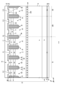
- FIG. 1 is a top view illustrating an example of a semiconductor device 100 according to an embodiment of the present invention.
- FIG. 2 is an enlarged view of an area D in FIG.
- FIG. 3 is a diagram showing an example of a cross section taken along the line ee in FIG. 2.
- 2 is an enlarged view of the vicinity of a first mesa portion 61, a second mesa portion 62, and a third mesa portion 63.
- FIG. 13 is another example of an enlarged view of the vicinity of the first mesa portion 61, the second mesa portion 62, and the third mesa portion 63.
- FIG. FIG. 3 is a diagram showing an example of the ff cross section in FIG. 2.
- 6 is an enlarged view of the vicinity of a first mesa portion 61, a second mesa portion 62, and a third mesa portion 63 shown in FIG. 5.
- 6 is an enlarged view of another example of the vicinity of the first mesa portion 61, the second mesa portion 62, and the third mesa portion 63 shown in FIG. 5.
- 6B is a diagram showing an example of a doping concentration distribution along the line aa and the line bb in FIG. 6A.
- FIG. 6C is a diagram showing an example of a doping concentration distribution along the line aa and the line bb in FIG. 6B.
- 2 is an enlarged view of the periphery of a first contact portion 211.
- FIG. 2 is an enlarged view of the periphery of a second contact portion 212.
- FIG. FIG. 13 is a diagram showing another example of the ee cross section. 2 is a diagram showing an example of the arrangement of adjustment regions 201 and non-adjustment regions 202 when viewed from above.
- FIG. FIG. 13 is a diagram showing another example of the ee cross section.
- FIG. 13 is a diagram showing another example of the ee cross section.
- FIG. 13 is a diagram showing another example of the ee cross section.
- FIG. 13 is a diagram showing another example of the ee cross section.
- FIG. 13 is a diagram showing another example of the ee cross section.
- FIG. 13 is a diagram showing another example of the ee cross section.
- FIG. 13 is a diagram showing another example of the ee cross section.
- one side in a direction parallel to the depth direction of the semiconductor substrate is referred to as "upper” and the other side as “lower.”
- the upper surface is referred to as the upper surface and the other surface is referred to as the lower surface.
- the directions of "upper” and “lower” are not limited to the direction of gravity or the directions when the semiconductor device is mounted.
- the orthogonal coordinate axes merely identify the relative positions of components, and do not limit a specific direction.
- the Z-axis does not limit the height direction relative to the ground.
- the +Z-axis direction and the -Z-axis direction are opposite directions.
- the Z-axis direction is described without indicating positive or negative, it means the direction parallel to the +Z-axis and -Z-axis.
- the orthogonal axes parallel to the top and bottom surfaces of the semiconductor substrate are referred to as the X-axis and Y-axis.
- the axis perpendicular to the top and bottom surfaces of the semiconductor substrate is referred to as the Z-axis.
- the direction of the Z-axis may be referred to as the depth direction.
- the direction parallel to the top and bottom surfaces of the semiconductor substrate, including the X-axis and Y-axis may be referred to as the horizontal direction.
- the region from the center of the semiconductor substrate in the depth direction to the top surface of the semiconductor substrate may be referred to as the top side.
- the region from the center of the semiconductor substrate in the depth direction to the bottom surface of the semiconductor substrate may be referred to as the bottom side.
- the conductivity type of a doped region doped with impurities is described as P type or N type.
- impurities may particularly mean either N type donors or P type acceptors, and may be described as dopants.
- doping means introducing donors or acceptors into a semiconductor substrate to make it a semiconductor that exhibits N type conductivity or P type conductivity.
- the doping concentration means the concentration of the donor or the concentration of the acceptor in a thermal equilibrium state.
- the net doping concentration means the net concentration obtained by adding up the donor concentration as the concentration of positive ions and the acceptor concentration as the concentration of negative ions, including the polarity of the charge.
- the donor concentration is N D and the acceptor concentration is N A
- the net doping concentration at any position is N D -N A.
- the net doping concentration may be simply referred to as the doping concentration.
- Donors have the function of supplying electrons to a semiconductor. Acceptors have the function of receiving electrons from a semiconductor. Donors and acceptors are not limited to impurities themselves.
- VOH defects in semiconductors which are formed by combining vacancies (V), oxygen (O), and hydrogen (H), function as donors that supply electrons.
- Hydrogen donors may be donors in which at least vacancies (V) and hydrogen (H) are combined.
- interstitial Si-H which is formed by combining interstitial silicon (Si-i) and hydrogen in a silicon semiconductor, also functions as a donor that supplies electrons.
- VOH defects or interstitial Si-H may be referred to as hydrogen donors.
- the semiconductor substrate has N-type bulk donors distributed throughout.
- the bulk donors are donors due to dopants contained substantially uniformly in the ingot during the manufacture of the ingot that is the basis of the semiconductor substrate.
- the bulk donors in this example are elements other than hydrogen.
- the dopants of the bulk donors are, for example, phosphorus, antimony, arsenic, selenium, or sulfur, but are not limited thereto.
- the bulk donors in this example are phosphorus.
- the bulk donors are also contained in the P-type region.
- the semiconductor substrate may be a wafer cut from a semiconductor ingot, or may be a chip obtained by dividing the wafer.
- the semiconductor ingot may be manufactured by any of the Czochralski method (CZ method), the magnetic field-applied Czochralski method (MCZ method), and the float zone method (FZ method).
- the ingot in this example is manufactured by the MCZ method.
- the oxygen concentration contained in the substrate manufactured by the MCZ method is 1 ⁇ 10 17 to 7 ⁇ 10 17 /cm 3.
- the oxygen concentration contained in the substrate manufactured by the FZ method is 1 ⁇ 10 15 to 5 ⁇ 10 16 /cm 3.
- the bulk donor concentration may be the chemical concentration of the bulk donors distributed throughout the semiconductor substrate, and may be a value between 90% and 100% of the chemical concentration.
- the semiconductor substrate may be a non-doped substrate that does not contain dopants such as phosphorus.
- the bulk donor concentration (D0) of the non-doped substrate is, for example, 1 ⁇ 10 10 /cm 3 or more and 5 ⁇ 10 12 /cm 3 or less.
- the bulk donor concentration (D0) of the non-doped substrate is preferably 1 ⁇ 10 11 /cm 3 or more.
- the bulk donor concentration (D0) of the non-doped substrate is preferably 5 ⁇ 10 12 /cm 3 or less.
- the respective concentrations in the present invention may be values at room temperature. As an example of the values at room temperature, values at 300 K (Kelvin) (approximately 26.9° C.) may be used.
- chemical concentration refers to the atomic density of an impurity measured regardless of the state of electrical activation.
- the chemical concentration can be measured, for example, by secondary ion mass spectrometry (SIMS).
- the above-mentioned net doping concentration can be measured by a voltage-capacitance measurement method (CV method).
- the carrier concentration measured by a spreading resistance measurement method (SR method) may be the net doping concentration.
- the carrier concentration measured by the CV method or the SR method may be a value in a thermal equilibrium state.
- the donor concentration is sufficiently larger than the acceptor concentration in an N-type region, the carrier concentration in that region may be the donor concentration.
- the carrier concentration in that region may be the acceptor concentration.
- the doping concentration in an N-type region may be referred to as the donor concentration
- the doping concentration in a P-type region may be referred to as the acceptor concentration.
- the peak value may be taken as the concentration of the donor, acceptor or net doping in the region.
- the concentration of the donor, acceptor or net doping is almost uniform, the average value of the concentration of the donor, acceptor or net doping in the region may be taken as the concentration of the donor, acceptor or net doping.
- atoms/cm 3 or /cm 3 is used to express concentration per unit volume. This unit is used for donor or acceptor concentration or chemical concentration in a semiconductor substrate. The notation of atoms may be omitted.
- the carrier concentration measured by the SR method may be lower than the donor or acceptor concentration.
- the carrier mobility of the semiconductor substrate may be lower than the value in the crystalline state. The reduction in carrier mobility occurs when the carriers are scattered due to disorder in the crystal structure caused by lattice defects, etc.
- the donor or acceptor concentration calculated from the carrier concentration measured by the CV method or the SR method may be lower than the chemical concentration of the element representing the donor or acceptor.
- the donor concentration of phosphorus or arsenic, which acts as a donor in a silicon semiconductor, or the acceptor concentration of boron, which acts as an acceptor is about 99% of the chemical concentration.
- the donor concentration of hydrogen, which acts as a donor in a silicon semiconductor is about 0.1% to 10% of the chemical concentration of hydrogen.
- FIG. 1 is a top view showing an example of a semiconductor device 100 according to one embodiment of the present invention.
- FIG. 1 the positions of each component projected onto the top surface of a semiconductor substrate 10 are shown.
- FIG. 1 only some of the components of the semiconductor device 100 are shown, and other components are omitted.
- the semiconductor device 100 includes a semiconductor substrate 10.
- the semiconductor substrate 10 is a substrate formed of a semiconductor material.
- the semiconductor substrate 10 is a silicon substrate.
- the semiconductor substrate 10 has edges 162 when viewed from above. When simply referred to as a top view in this specification, it means that the semiconductor substrate 10 is viewed from the top side.
- the semiconductor substrate 10 has two sets of edges 162 that face each other when viewed from above. In FIG. 1, the X-axis and Y-axis are parallel to one of the edges 162. The Z-axis is perpendicular to the top surface of the semiconductor substrate 10.
- the semiconductor substrate 10 has an active portion 160.
- the active portion 160 is a region where a main current flows in the depth direction between the upper and lower surfaces of the semiconductor substrate 10 when the semiconductor device 100 is operating.
- An emitter electrode is provided above the active portion 160, but is omitted in FIG. 1.
- the active portion 160 may refer to the region that overlaps with the emitter electrode when viewed from above.
- the active portion 160 may also include the region sandwiched between the active portions 160 when viewed from above.
- the active section 160 includes a transistor section 70 including a transistor element such as an IGBT (Insulated Gate Bipolar Transistor), and a diode section 80 including a diode element such as a free wheel diode (FWD).
- the transistor sections 70 and the diode sections 80 are alternately arranged along a predetermined first direction (the X-axis direction in this example) on the upper surface of the semiconductor substrate 10.
- the semiconductor device 100 in this example is a reverse conducting IGBT (RC-IGBT).
- a boundary region is arranged between the transistor section 70 and the diode section 80 in the X-axis direction, but is omitted in FIG. 1.
- a direction different from the first direction in a top view may be referred to as a second direction (the Y-axis direction in FIG. 1).
- the second direction may be perpendicular to the first direction.
- the transistor section 70 and the diode section 80 may each have a longitudinal direction in the second direction. That is, the length of the transistor section 70 in the Y-axis direction is greater than its width in the X-axis direction. Similarly, the length of the diode section 80 in the Y-axis direction is greater than its width in the X-axis direction.
- the second direction of the transistor section 70 and the diode section 80 may be the same as the longitudinal direction of each trench section and the longitudinal direction of the mesa section, which will be described later.
- the diode section 80 has an N+ type cathode region in a region that contacts the lower surface of the semiconductor substrate 10.
- the region in which the cathode region is provided is referred to as the diode section 80.
- the diode section 80 is a region that overlaps with the cathode region when viewed from above.
- a P+ type collector region may be provided in a region other than the cathode region on the lower surface of the semiconductor substrate 10.
- an extension region 81 that extends the diode section 80 in the Y-axis direction to the gate wiring described below may also be included in the diode section 80.
- a collector region is provided on the lower surface of the extension region 81.
- the transistor section 70 has a P+ type collector region in a region that contacts the bottom surface of the semiconductor substrate 10.
- the transistor section 70 has a gate structure that has an N type emitter region, a P type base region, a gate conductive portion, and a gate insulating film periodically arranged on the top surface side of the semiconductor substrate 10.
- the semiconductor device 100 may have one or more pads above the semiconductor substrate 10.
- the semiconductor device 100 in this example has a gate pad 164.
- the semiconductor device 100 may also have pads such as an anode pad, a cathode pad, and a current detection pad.
- Each pad is disposed near an edge 162.
- the vicinity of the edge 162 refers to the area between the edge 162 and the emitter electrode in a top view.
- each pad may be connected to an external circuit via wiring such as a wire.
- a gate potential is applied to the gate pad 164.
- the gate pad 164 is electrically connected to the conductive portion of the gate trench portion of the active portion 160.
- the semiconductor device 100 includes a gate wiring that connects the gate pad 164 and the gate trench portion. In FIG. 1, the gate wiring is hatched with diagonal lines.
- the gate wiring in this example has a peripheral gate wiring 130 and an active side gate wiring 131.
- the peripheral gate wiring 130 is disposed between the active portion 160 and an edge 162 of the semiconductor substrate 10 in a top view.
- the peripheral gate wiring 130 in this example surrounds the active portion 160 in a top view.
- the region surrounded by the peripheral gate wiring 130 in a top view may be the active portion 160.
- a well region is formed below the gate wiring.
- the well region is a P-type region with a higher concentration than the base region described below, and is formed from the top surface of the semiconductor substrate 10 to a position deeper than the base region.
- the region surrounded by the well region in a top view may be the active portion 160.
- the peripheral gate wiring 130 is connected to the gate pad 164.
- the peripheral gate wiring 130 is disposed above the semiconductor substrate 10.
- the peripheral gate wiring 130 may be a metal wiring containing aluminum or the like, or a wiring formed of a semiconductor such as polysilicon doped with impurities.
- the active side gate wiring 131 is provided in the active section 160. By providing the active side gate wiring 131 in the active section 160, the variation in wiring length from the gate pad 164 can be reduced for each region of the semiconductor substrate 10.
- the peripheral gate wiring 130 and the active side gate wiring 131 are connected to the gate trench portion of the active section 160.
- the peripheral gate wiring 130 and the active side gate wiring 131 are disposed above the semiconductor substrate 10.
- the peripheral gate wiring 130 and the active side gate wiring 131 may be metal wiring containing aluminum or the like, or wiring formed of a semiconductor such as polysilicon doped with impurities.
- the active side gate wiring 131 may be connected to the peripheral gate wiring 130.
- the active side gate wiring 131 is provided extending in the X-axis direction from one peripheral gate wiring 130 to the other peripheral gate wiring 130 sandwiching the active section 160, so as to cross the active section 160 at approximately the center in the Y-axis direction.
- the transistor section 70 and the diode section 80 may be arranged alternately in the X-axis direction in each divided region.
- the semiconductor device 100 may also include a temperature sensor (not shown) that is a PN junction diode formed of polysilicon or the like, and a current detector (not shown) that simulates the operation of a transistor section provided in the active section 160.
- a temperature sensor not shown
- a current detector not shown
- the semiconductor device 100 includes an edge termination structure 90 between the active portion 160 and the edge 162 when viewed from above.
- the edge termination structure 90 in this example is disposed between the peripheral gate wiring 130 and the edge 162.
- the edge termination structure 90 reduces electric field concentration on the upper surface side of the semiconductor substrate 10.
- the edge termination structure 90 may include at least one of a guard ring, a field plate, and a resurf that are arranged in a ring shape surrounding the active portion 160.
- Region D includes transistor section 70, diode section 80, and active side gate wiring 131. Although omitted in FIG. 1, a boundary region 200 is disposed between transistor section 70 and diode section 80 in the X-axis direction.
- the semiconductor device 100 of this example includes a gate trench section 40, a dummy trench section 30, a well region 11, an emitter region 12, a base region 14, and a contact region 15 provided inside the upper surface side of the semiconductor substrate 10.
- the gate trench section 40 and the dummy trench section 30 are each an example of a trench section.
- the semiconductor device 100 of this example also includes an emitter electrode 52 and an active side gate wiring 131 provided above the upper surface of the semiconductor substrate 10.
- the emitter electrode 52 is an example of a metal electrode.
- the emitter electrode 52 and the active side gate wiring 131 are provided separately from each other.
- An interlayer insulating film is provided between the emitter electrode 52 and the active gate wiring 131 and the upper surface of the semiconductor substrate 10, but is omitted in FIG. 2.
- contact holes 54 are provided in the interlayer insulating film, penetrating the interlayer insulating film. In FIG. 2, each contact hole 54 is hatched with diagonal lines.
- the emitter electrode 52 is provided above the gate trench portion 40, the dummy trench portion 30, the well region 11, the emitter region 12, the base region 14, and the contact region 15.
- the emitter electrode 52 contacts the emitter region 12, the contact region 15, and the base region 14 on the upper surface of the semiconductor substrate 10 through a contact hole 54.
- the emitter electrode 52 is also connected to the dummy conductive portion in the dummy trench portion 30 through a contact hole provided in the interlayer insulating film.
- the emitter electrode 52 may be connected to the dummy conductive portion of the dummy trench portion 30 at the tip of the dummy trench portion 30 in the Y-axis direction.
- the dummy conductive portion of the dummy trench portion 30 does not need to be connected to the emitter electrode 52 and the gate conductive portion, and may be controlled to a potential different from the potential of the emitter electrode 52 and the potential of the gate conductive portion.
- the active side gate wiring 131 is connected to the gate trench portion 40 through a contact hole provided in the interlayer insulating film.
- the active side gate wiring 131 may be connected to the gate conductive portion of the gate trench portion 40 at the tip portion 41 of the gate trench portion 40 in the Y-axis direction.
- the active side gate wiring 131 is not connected to the dummy conductive portion in the dummy trench portion 30.
- the emitter electrode 52 is formed of a material containing metal.
- FIG. 2 shows the range in which the emitter electrode 52 is provided.
- the emitter electrode 52 is formed of aluminum or an aluminum-silicon alloy, such as a metal alloy such as AlSi or AlSiCu.
- the emitter electrode 52 may have a barrier metal made of titanium or a titanium compound under the region made of aluminum or the like.
- the emitter electrode 52 may have a plug portion formed by embedding tungsten or the like in the contact hole so as to contact the barrier metal and aluminum or the like.
- the well region 11 is provided so as to overlap with the active side gate wiring 131.
- the well region 11 is also provided so as to extend by a predetermined width into an area where it does not overlap with the active side gate wiring 131.
- the well region 11 is provided away from the end of the contact hole 54 in the Y-axis direction toward the active side gate wiring 131.
- the well region 11 is a region of a second conductivity type having a higher doping concentration than the base region 14.
- the base region 14 is P type
- the well region 11 is P+ type.
- the transistor section 70, the diode section 80, and the boundary region 200 each have a plurality of trench sections arranged in a first direction.
- one or more gate trench sections 40 and one or more dummy trench sections 30 are alternately provided along the first direction.
- a plurality of dummy trench sections 30 are provided along the first direction.
- no gate trench section 40 is provided in the diode section 80 of this example.
- a plurality of dummy trench sections 30 are provided along the first direction.
- no gate trench section 40 is provided.
- the gate trench portion 40 in this example may have two straight portions 39 (portions of the trench that are straight along the second direction) that extend along a second direction perpendicular to the first direction, and a tip portion 41 that connects the two straight portions 39.
- the second direction in FIG. 2 is the Y-axis direction.
- the tip 41 is curved when viewed from above.
- the tip 41 connects the ends of the two straight portions 39 in the Y-axis direction, thereby reducing electric field concentration at the ends of the straight portions 39.
- the dummy trench portion 30 is provided between each straight portion 39 of the gate trench portion 40.
- One dummy trench portion 30 may be provided between each straight portion 39, or multiple dummy trench portions 30 may be provided.
- the dummy trench portion 30 may have a straight line shape extending in the second direction, and may have a straight line portion 29 and a tip portion 31, similar to the gate trench portion 40.
- the semiconductor device 100 shown in FIG. 2 includes both a straight line dummy trench portion 30 without a tip portion 31 and a dummy trench portion 30 with a tip portion 31.
- the diffusion depth of the well region 11 may be deeper than the depth of the gate trench portion 40 and the dummy trench portion 30.
- the ends in the Y-axis direction of the gate trench portion 40 and the dummy trench portion 30 are provided in the well region 11 when viewed from above. In other words, at the ends in the Y-axis direction of each trench portion, the bottoms in the depth direction of each trench portion are covered by the well region 11. This makes it possible to reduce electric field concentration at the bottoms of each trench portion.
- the mesa portions 60 are provided between the trench portions in the first direction.
- the mesa portions 60 refer to the regions sandwiched between the trench portions inside the semiconductor substrate 10.
- the upper end of the mesa portion 60 is the upper surface of the semiconductor substrate 10.
- the depth position of the lower end of the mesa portion 60 is the same as the depth position of the lower end of the trench portion.
- the mesa portion 60 is provided on the upper surface of the semiconductor substrate 10, extending in the second direction (Y-axis direction) along the trench.
- the mesa portion 60 of the transistor portion 70, the mesa portion 60 of the diode portion 80, and the mesa portion 60 of the boundary region 200 may have different structures.
- the term "mesa portion 60" refers to each of the mesa portion 60 of the transistor portion 70, the mesa portion 60 of the diode portion 80, and the mesa portion 60 of the boundary region 200.
- a base region 14 is provided in each mesa portion 60. Of the base regions 14 exposed on the upper surface of the semiconductor substrate 10 in the mesa portion 60, the region closest to the active side gate wiring 131 is referred to as the base region 14-e. In FIG. 2, the base region 14-e is shown to be located at one end of each mesa portion in the second direction, but the base region 14-e is also located at the other end of each mesa portion.
- at least one of the emitter region 12 of the first conductivity type and the contact region 15 of the second conductivity type may be provided in the region sandwiched between the base regions 14-e in a top view.
- the emitter region 12 is N+ type
- the contact region 15 is P+ type.
- the emitter region 12 and the contact region 15 may be provided between the base region 14 and the upper surface of the semiconductor substrate 10 in the depth direction.
- the mesa portion 60 of the transistor portion 70 has an emitter region 12 exposed on the upper surface of the semiconductor substrate 10.
- the emitter region 12 is provided in contact with the gate trench portion 40.
- the mesa portion 60 in contact with the gate trench portion 40 may have a contact region 15 exposed on the upper surface of the semiconductor substrate 10.
- the contact regions 15 and emitter regions 12 in the mesa portion 60 are each provided from one trench portion to the other trench portion in the X-axis direction. As an example, the contact regions 15 and emitter regions 12 in the mesa portion 60 are alternately arranged along the second direction (Y-axis direction) of the trench portion.
- the contact region 15 and emitter region 12 of the mesa portion 60 may be provided in a stripe shape along the second direction (Y-axis direction) of the trench portion.
- the emitter region 12 is provided in a region that contacts the trench portion, and the contact region 15 is provided in a region sandwiched between the emitter regions 12.
- the mesa portion 60 of the diode portion 80 and the boundary region 200 does not have an emitter region 12.
- the upper surface of the mesa portion 60 of the diode portion 80 and the boundary region 200 may have a base region 14 and a contact region 15.
- a contact region 15 may be provided in contact with each of the base regions 14-e.
- a base region 14 may be provided in the region sandwiched between the contact regions 15 on the upper surface of the mesa portion 60 of the diode portion 80.
- the base region 14 may be disposed in the entire region sandwiched between the contact regions 15.
- the mesa portion 60 of the boundary region 200 may have the same structure as the mesa portion 60 of the diode portion 80, or may have a different structure.
- a contact region 15 is provided in the entire region sandwiched between the base regions 14-e. That is, the area of the contact region 15 of the mesa portion 60 in the boundary region 200 may be larger than the area of the contact region 15 of the mesa portion 60 in the diode portion 80. In this case, holes in the semiconductor substrate 10 are easily extracted to the emitter electrode 52 through the mesa portion 60 in the boundary region 200.
- the mesa portion 60 of the boundary region 200 may be a P-type impurity region having a doping concentration similar to or lower than that of the base region 14 of the transistor portion 70.
- the P-type impurity region may occupy the entire mesa portion 60 of the boundary region 200, or other regions may be provided in the mesa portion 60 of the boundary region 200.
- an N-type impurity region having a doping concentration similar to or lower than that of the emitter region 12 may be provided in the mesa portion 60 of the boundary region 200.
- the gate trench portion 40 is not provided in the boundary region 200.
- the trench portion at the boundary between the transistor portion 70 and the boundary region 200 is a dummy trench portion 30. Since the N-type impurity region of the mesa portion 60 of the boundary region 200 does not contact the gate trench portion 40, no more current flows in the boundary region 200 than in the transistor portion 70. This suppresses the injection of holes from the mesa portion 60 of the boundary region 200, and reduces reverse recovery loss.
- a contact hole 54 is provided above each mesa portion 60.
- the contact hole 54 is located in a region sandwiched between the base regions 14-e.
- the contact holes 54 are provided above the contact region 15, the base region 14, and the emitter region 12.
- the contact holes 54 are not provided in the regions corresponding to the base region 14-e and the well region 11.
- the contact hole 54 may be located in the center of the mesa portion 60 in the first direction (X-axis direction).
- an N+ type cathode region 82 is provided in a region adjacent to the underside of the semiconductor substrate 10.
- a P+ type collector region 22 may be provided in the region of the underside of the semiconductor substrate 10 where the cathode region 82 is not provided.
- the cathode region 82 and the collector region 22 are provided between the underside 23 of the semiconductor substrate 10 and the buffer region 20.
- the boundary between the cathode region 82 and the collector region 22 is indicated by a dotted line.
- the cathode region 82 is disposed away from the well region 11 in the Y-axis direction. This ensures a distance between the cathode region 82 and the P-type region (well region 11), which has a relatively high doping concentration and is formed deep, and improves the breakdown voltage.
- the end of the cathode region 82 in the Y-axis direction is disposed farther from the well region 11 than the end of the contact hole 54 in the Y-axis direction.
- the end of the cathode region 82 in the Y-axis direction may be disposed between the well region 11 and the contact hole 54.
- FIG. 3 is a diagram showing an example of the e-e cross section in FIG. 2.
- the e-e cross section is an XZ plane passing through the emitter region 12 and the cathode region 82.
- the semiconductor device 100 of this example has a semiconductor substrate 10, an interlayer insulating film 38, an emitter electrode 52, and a collector electrode 24.
- the interlayer insulating film 38 is provided on the upper surface of the semiconductor substrate 10.
- the interlayer insulating film 38 is a film that includes at least one layer of an insulating film such as silicate glass doped with impurities such as boron or phosphorus, a thermal oxide film, and other insulating films.
- the interlayer insulating film 38 is provided with the contact hole 54 described in FIG. 2.
- the emitter electrode 52 is provided above the interlayer insulating film 38.
- the emitter electrode 52 is in contact with the upper surface 21 of the semiconductor substrate 10 through a contact hole 54 in the interlayer insulating film 38.
- the collector electrode 24 is provided on the lower surface 23 of the semiconductor substrate 10.
- the emitter electrode 52 and the collector electrode 24 are formed of a metal material such as aluminum.
- the direction connecting the emitter electrode 52 and the collector electrode 24 (Z-axis direction) is referred to as the depth direction.
- the emitter electrode 52 may have a barrier metal containing titanium in a portion that contacts the upper surface 21 of the semiconductor substrate 10.
- the barrier metal may have a titanium nitride layer, or may have a laminated structure of a titanium nitride layer and a titanium layer.
- the emitter electrode 52 may have a plug portion of tungsten or the like filled inside the contact hole 54. The plug portion may also be provided in a trench contact portion described later.
- the semiconductor substrate 10 has an N-type or N-type drift region 18.
- the drift region 18 is provided in each of the transistor portion 70, the diode portion 80, and the boundary region 200.
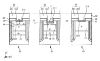
- the multiple mesa portions 60 include a first mesa portion 61, a second mesa portion 62, a third mesa portion 63, and a fourth mesa portion 64.
- the first mesa portion 61 and the second mesa portion 62 are provided in the transistor portion 70
- the third mesa portion 63 is provided in the diode portion 80
- the fourth mesa portion 64 is provided in the boundary region 200.
- an N+ type emitter region 12 and a P type base region 14 are provided in this order from the upper surface 21 side of the semiconductor substrate 10.
- a drift region 18 is provided below the base region 14.
- An N+ type accumulation region 16 may be provided in the first mesa portion 61 and the second mesa portion 62. The accumulation region 16 is disposed between the base region 14 and the drift region 18.
- the emitter region 12 is exposed on the upper surface 21 of the semiconductor substrate 10 and is provided in contact with the gate trench portion 40.
- the emitter region 12 may be in contact with the trench portions on both sides of the mesa portion 60.
- the emitter region 12 has a higher doping concentration than the drift region 18.
- the base region 14 is provided below the emitter region 12. In this example, the base region 14 is provided in contact with the emitter region 12. The base region 14 may be in contact with the trench portions on both sides of the first mesa portion 61 and the second mesa portion 62.
- the accumulation region 16 is provided below the base region 14.
- the accumulation region 16 is an N+ type region with a higher doping concentration than the drift region 18. In other words, the accumulation region 16 has a higher donor concentration than the drift region 18.
- the carrier injection enhancement effect IE effect
- the accumulation region 16 may be provided so as to cover the entire lower surface of the base region 14 in the first mesa portion 61 and the second mesa portion 62.
- the third mesa portion 63 of the diode portion 80 has a P-type base region 14 in contact with the upper surface 21 of the semiconductor substrate 10.
- the base region 14 of the third mesa portion 63 may be referred to as an anode region.
- the doping concentration of the base region 14 of the third mesa portion 63 may be the same as or smaller than the doping concentration of the base regions 14 of the first mesa portion 61 and the second mesa portion 62.
- a drift region 18 is provided below the base region 14.
- An accumulation region 16 may be provided below the base region 14 in the third mesa portion 63.
- a P+ type contact region 15 is provided in the fourth mesa portion 64 of the boundary region 200 in contact with the upper surface 21 of the semiconductor substrate 10.
- a drift region 18 is provided below the contact region 15.
- a base region 14 may be provided between the contact region 15 and the drift region 18.
- An accumulation region 16 may be provided below the base region 14 in the fourth mesa portion 64.
- an N+ type buffer region 20 may be provided below the drift region 18.
- the doping concentration of the buffer region 20 is higher than the doping concentration of the drift region 18.
- the buffer region 20 may have a concentration peak with a higher doping concentration than the drift region 18.
- the doping concentration of the concentration peak refers to the doping concentration at the apex of the concentration peak.
- the doping concentration of the drift region 18 may be the average value of the doping concentration in a region where the doping concentration distribution is approximately flat.
- the buffer region 20 may have two or more concentration peaks in the depth direction (Z-axis direction) of the semiconductor substrate 10.
- the concentration peak of the buffer region 20 may be located at the same depth as the chemical concentration peak of hydrogen (protons) or phosphorus, for example.
- the buffer region 20 may function as a field stop layer that prevents the depletion layer spreading from the lower end of the base region 14 from reaching the P+ type collector region 22 and the N+ type cathode region 82.
- a P+ type collector region 22 is provided below the buffer region 20.
- the acceptor concentration of the collector region 22 is higher than the acceptor concentration of the base region 14.
- the collector region 22 may contain the same acceptor as the base region 14, or may contain a different acceptor.
- the acceptor of the collector region 22 is, for example, boron.
- an N+ type cathode region 82 is provided below the buffer region 20.
- the donor concentration of the cathode region 82 is higher than the donor concentration of the drift region 18.
- the donor of the cathode region 82 is, for example, hydrogen or phosphorus. Note that the elements that serve as the donor and acceptor of each region are not limited to the above-mentioned examples.
- a P+ type collector region 22 is provided under the buffer region 20.
- the collector region 22 in the boundary region 200 may have the same doping concentration as the boundary region 200 of the transistor section 70.
- the boundary position in the X-axis direction between the cathode region 82 and the collector region 22 may be the boundary position in the X-axis direction between the diode section 80 and the boundary region 200.
- a part or all of the collector region 22 may be replaced with the cathode region 82.
- the region in which the contact region 15 and the base region 14 are alternately arranged in the region sandwiched between the base regions 14-e may be the diode section 80, and the region in which the contact region 15 is arranged over the entire region sandwiched between the base regions 14-e may be the boundary region 200.
- the boundary region 200 may be regarded as part of the diode section 80.
- the gate trench portion 40 arranged closest to the diode portion 80 in the X-axis direction is set as the boundary position in the X-axis direction between the transistor portion 70 and the boundary region 200 (or the diode portion 80).
- the center position in the X-axis direction of the gate trench portion 40 may be set as the boundary position in the X-axis direction between the transistor portion 70 and the boundary region 200 (or the diode portion 80).
- the trench portion on the diode portion 80 side may be the dummy trench portion 30.
- the dummy trench portion 30 may be set as the boundary position in the X-axis direction between the transistor portion 70 and the boundary region 200 (or the diode portion 80).
- the boundary region 200 may be provided with an emitter region 12. In that case, however, no gate trench portion 40 is provided in the boundary region 200. Also, the trench portion at the boundary position between the transistor portion 70 and the boundary region 200 is a dummy trench portion 30. In other words, no transistor operation occurs in the boundary region 200.
- the boundary region 200 may be provided with a gate trench portion 40. In that case, however, no emitter region 12 is provided in the boundary region 200. In other words, no transistor operation occurs in the boundary region 200.
- the collector region 22 and the cathode region 82 are exposed on the lower surface 23 of the semiconductor substrate 10 and are connected to the collector electrode 24.
- the collector electrode 24 may be in contact with the entire lower surface 23 of the semiconductor substrate 10.
- the emitter electrode 52 and the collector electrode 24 are formed of a metal material such as aluminum.
- each trench portion is provided from the upper surface 21 of the semiconductor substrate 10, penetrating the base region 14, to below the base region 14. In regions where at least one of the emitter region 12, the contact region 15, and the accumulation region 16 is provided, each trench portion also penetrates these doped regions.
- the trench portion penetrating the doped region is not limited to being manufactured in the order of forming the doped region and then the trench portion.
- the trench portion penetrating the doped region also includes a trench portion formed after the trench portion is formed.
- the transistor section 70 is provided with a gate trench section 40 and a dummy trench section 30.
- the diode section 80 and the boundary region 200 are provided with a dummy trench section 30, but not with a gate trench section 40.
- a gate trench section 40 or a dummy trench section 30 may be arranged at the boundary between the boundary region 200 and the transistor section 70.
- the boundary region 200 is a buffer structure for arranging the different structures of the transistor section 70 and the diode section 80 in parallel. Therefore, the width of the boundary region 200 in the X-axis direction may be short.
- the fourth mesa section 64 of the boundary region 200 may be provided over a width of one or several sections. In other examples, the boundary region 200 may not be provided.
- the width of the boundary region 200 in the X-axis direction may be set wide across multiple fourth mesa portions 64. This makes it possible to suppress the influence of the transistor portion 70 on the characteristics of the diode portion 80, for example, the influence of the operation of the gate trench portion 40 and the ejection or injection of holes in the contact region 15 on the forward voltage and reverse recovery characteristics.
- the number of mesa portions refers to the number of mesa portions arranged side by side in the X-axis direction.
- the gate trench portion 40 has a gate trench provided on the upper surface 21 of the semiconductor substrate 10, a gate insulating film 42, and a gate conductive portion 44.
- the gate insulating film 42 is provided to cover the inner wall of the gate trench.
- the gate insulating film 42 may be formed by oxidizing or nitriding the semiconductor on the inner wall of the gate trench.
- the gate conductive portion 44 is provided inside the gate insulating film 42 inside the gate trench. In other words, the gate insulating film 42 insulates the gate conductive portion 44 from the semiconductor substrate 10.
- the gate conductive portion 44 is formed of a conductive material such as polysilicon.
- the gate conductive portion 44 may be provided longer than the base region 14 in the depth direction.
- the gate trench portion 40 in this cross section is covered by the interlayer insulating film 38 on the upper surface 21 of the semiconductor substrate 10.
- the gate conductive portion 44 is electrically connected to the gate wiring. When a predetermined gate voltage is applied to the gate conductive portion 44, a channel is formed by an electron inversion layer in the surface layer of the interface of the base region 14 that contacts the gate trench portion 40.
- the dummy trench portion 30 may have the same structure as the gate trench portion 40 in the cross section.
- the dummy trench portion 30 has a dummy trench, a dummy insulating film 32, and a dummy conductive portion 34 provided on the upper surface 21 of the semiconductor substrate 10.
- the dummy conductive portion 34 is electrically connected to the emitter electrode 52.
- the dummy insulating film 32 is provided to cover the inner wall of the dummy trench.
- the dummy conductive portion 34 is provided inside the dummy trench and is provided on the inside of the dummy insulating film 32.
- the dummy insulating film 32 insulates the dummy conductive portion 34 from the semiconductor substrate 10.
- the dummy conductive portion 34 may be formed of the same material as the gate conductive portion 44.
- the dummy conductive portion 34 is formed of a conductive material such as polysilicon.
- the dummy conductive portion 34 may have the same length in the depth direction as the gate conductive portion 44.
- the gate trench portion 40 and the dummy trench portion 30 are covered by an interlayer insulating film 38 on the upper surface 21 of the semiconductor substrate 10.
- the bottoms of the dummy trench portion 30 and the gate trench portion 40 may be curved and convex downward (curved in cross section).
- the transistor section 70 has a first contact section 211 and a second contact section 212.
- the first contact section 211 is a section where the first mesa section 61 and the emitter electrode 52 contact each other.
- the second contact section 212 is a section where the second mesa section 62 and the emitter electrode 52 contact each other.
- the second mesa section 62 is disposed farther from the diode section 80 in the X-axis direction than the first mesa section 61. That is, in the X-axis direction, the distance between the diode section 80 and the second mesa section 62 is greater than the distance between the diode section 80 and the first mesa section 61.
- the second contact section 212 is disposed farther from the diode section 80 in the X-axis direction than the first contact section 211. That is, in the X-axis direction, the distance between the diode section 80 and the second contact section 212 is greater than the distance between the diode section 80 and the first contact section 211.
- the semiconductor device 100 may include a lifetime adjustment region 206 including a lifetime killer that adjusts the lifetime of carriers.
- the lifetime adjustment region 206 in this example is a region in which the lifetime of charge carriers is locally small.
- the charge carriers are electrons or holes.
- the charge carriers may simply be referred to as carriers.
- the lifetime adjustment region 206 in this example is formed by injecting charged particles such as helium ions from the upper surface 21 side of the semiconductor substrate 10.
- the concentration distribution of helium, etc. in the depth direction of the semiconductor substrate 10 may have a shape that trails from the lifetime adjustment region 206 to the upper surface 21 of the semiconductor substrate 10. That is, the concentration (/cm 3 ) of helium, etc. may monotonically decrease from the lifetime adjustment region 206 to the upper surface 21.
- the concentration of helium, etc. on the upper surface 21 may be greater than 0.
- the concentration of helium, etc. may also have a shape that trails in the direction from the lifetime adjustment region 206 toward the lower surface 23. However, the concentration of helium, etc. decreases more steeply toward the bottom surface 23 than toward the top surface 21.
- the concentration of helium, etc. at the bottom surface 23 is lower than the concentration of helium, etc. at the top surface 21.
- the concentration of helium, etc. at the top surface 21 may be below the measurement limit, or may be zero.
- the lifetime adjusting region 206 may be formed by injecting charged particles, such as helium ions, from the bottom surface 23 side of the semiconductor substrate 10.
- lattice defects 204 such as vacancies are formed near the injection position.
- the lattice defects 204 generate recombination centers.
- the lattice defects 204 may be mainly vacancies such as monovacancies (V) and divacancies (VV), or may be dislocations, interstitial atoms, transition metals, etc. For example, atoms adjacent to the vacancies have dangling bonds.
- the lattice defects 204 may also include donors and acceptors, but in this specification, the lattice defects 204 mainly composed of vacancies may be referred to as vacancy-type lattice defects, vacancy-type defects, or simply lattice defects.
- the lattice defects 204 may be referred to simply as recombination centers or lifetime killers as recombination centers that contribute to carrier recombination.
- the lifetime killers may be formed by injecting helium ions into the semiconductor substrate 10.
- the helium chemical concentration may be the density of the lattice defects 204.
- the lifetime killer formed by implanting helium ions may be terminated by hydrogen present in the buffer region 20, so the depth position of the lifetime killer density peak may not coincide with the depth position of the helium chemical concentration peak.
- the lifetime killer may be formed in the hydrogen ion passage region on the implantation surface side of the range when hydrogen ions are implanted into the semiconductor substrate 10.
- the lattice defect 204 is an example of a lifetime killer.
- the lattice defect 204 at the injection position of the charged particle is shown as a schematic cross.
- regions where many lattice defects 204 remain carriers are captured by the lattice defects 204, shortening the carrier lifetime.
- the characteristics of the diode section 80 such as the reverse recovery time and reverse recovery loss.
- the position where the carrier lifetime shows a minimum value may be set as the depth position of the lifetime adjustment region 206.
- the lifetime adjustment region 206 is disposed on the upper surface 21 side of the semiconductor substrate 10.
- the upper surface 21 side is the region from the center position in the depth direction of the semiconductor substrate 10 to the upper surface 21 of the semiconductor substrate 10.
- the lifetime adjustment region 206 is disposed below the lower end of the trench portion.
- the lifetime adjustment region 206 is formed by irradiation with a particle beam with high penetrating power, such as an electron beam, lattice defects are formed approximately uniformly from the upper surface 21 to the lower surface 23 of the semiconductor substrate 10, and even in this case, the depth position of the lifetime adjustment region 206 can be considered to be located on the upper surface 21 side of the semiconductor substrate 10.
- a particle beam with high penetrating power such as an electron beam
- the lifetime adjustment region 206 may be provided in at least one of the transistor portion 70 and the diode portion 80. If the semiconductor device 100 has a boundary region 200, the lifetime adjustment region 206 may also be provided in the boundary region 200. The lifetime adjustment region 206 may be provided over the entire diode portion 80 in the X-axis direction. The lifetime adjustment region 206 may also be provided over the entire boundary region 200.
- the lifetime adjustment region 206 of the diode section 80 may be provided extending in the X-axis direction up to a part of the transistor section 70.
- the lifetime adjustment region 206 of the diode section 80 and the lifetime adjustment region 206 of the transistor section 70 are provided at the same depth position.
- the region where the lifetime adjustment region 206 is provided is defined as the adjustment region 201
- the region where the lifetime adjustment region 206 is not provided is defined as the non-adjustment region 202.
- the non-adjustment region 202 is a region in which the carrier lifetime at the same depth position as the lifetime adjustment region 206 is longer than the carrier lifetime of the lifetime adjustment region 206 of the diode section 80.
- the non-adjustment region 202 may be a region in which charged particles such as helium ions for forming lifetime killers such as lattice defects 204 are not implanted.
- the chemical concentration (/cm 3 ) of helium or the like in the non-adjustment region 202 may be the same as the chemical concentration of the charged particles at the center of the drift region 18 in the Z-axis direction.
- a lifetime adjustment region 206 may be provided below at least a portion of the first mesa portion 61 and the first contact portion 211.
- a lifetime adjustment region 206 may be provided below a portion of the first mesa portion 61 and the first contact portion 211, or a lifetime adjustment region 206 may be provided below all of the first mesa portion 61 and the first contact portion 211.
- a lifetime adjustment region 206 may be provided below at least a portion of the second mesa portion 62 and the second contact portion 212.
- a lifetime adjustment region 206 may be provided below a portion of the second mesa portion 62 and the second contact portion 212, or a lifetime adjustment region 206 may be provided below all of the second mesa portion 62 and the second contact portion 212.
- the lifetime adjustment region 206 may be provided below the first mesa portion 61 and/or the diode portion 80. In the example of FIG. 3, the lifetime adjustment region 206 is provided below the first mesa portion 61 and in the diode portion 80.
- the lifetime adjustment region 206 may be provided below the first mesa portion 61, below the second mesa portion 62, and/or the diode portion 80. In the example of FIG. 3, the lifetime adjustment region 206 is provided below the first mesa portion 61, below the second mesa portion 62, and in all of the diode portion 80.
- the diode section 80 has a third contact section 213 that contacts the third mesa section 63 and the emitter electrode 52.
- the third contact section 213 may be provided for some of the third mesa sections 63, or may be provided for all of the third mesa sections 63.
- the boundary region 200 has a third contact section 213 that contacts the fourth mesa section 64 and the emitter electrode 52. In other words, the boundary region 200 has a third contact section 213 that has the same structure as the diode section 80.
- the third contact section 213 may be provided for some of the fourth mesa sections 64, or may be provided for all of the fourth mesa sections 64.
- each contact portion refers to the interface where the emitter electrode 52 and the semiconductor substrate 10 are in contact.
- the contact portion may include the surface of the emitter electrode 52 and the surface of the semiconductor substrate 10. If a metal silicide layer is formed at the interface between the emitter electrode 52 and the semiconductor substrate 10, the metal silicide layer may be included in the emitter electrode 52 (metal electrode). In other words, the interface between the metal silicide layer and the semiconductor substrate 10 may be considered as the contact portion.
- a trench contact portion 17 may be provided in at least a portion of the mesa portion 60.
- the trench contact portion 17 is a portion in which a metal electrode such as an emitter electrode 52 is provided inside the semiconductor substrate 10.
- the trench contact portion 17 can be formed by forming a groove in the upper surface 21 of the semiconductor substrate 10 exposed by the contact hole 54 and filling the inside of the groove with a metal electrode.
- the region in which the mesa portion 60 and a metal electrode such as the emitter electrode 52 contact each other in the trench contact portion 17 corresponds to the contact portion.
- the trench contact portion 17 is provided in the first mesa portion 61.
- a plug region may be provided in at least a portion of the mesa portion 60 in a region that contacts the lower end of the contact portion.
- the plug region is a P++ type region that has a higher doping concentration than the contact region 15.
- a third plug region 223 is provided in contact with the third contact portion 213.
- the first contact portion 211 of the first mesa portion 61 shown in FIG. 3 may be provided at a depth shallower than the lower end of the emitter region 12.
- the first plug region 221 is not provided at the lower end of the first contact portion 211.
- the first contact portion 211 may be provided at a depth that reaches the base region 14, and the first plug region 221 may be provided so as to contact the lower end of the first contact portion 211.
- FIG. 4A is an enlarged view of the vicinity of the first mesa portion 61, the second mesa portion 62, and the third mesa portion 63.
- FIG. 4A one each of the first mesa portion 61, the second mesa portion 62, and the third mesa portion 63 is shown, and the areas between each mesa portion are omitted.
- the depth position of the lower end of the first contact portion 211 is Z1
- the depth position of the lower end of the second contact portion 212 is Z2
- the depth position of the lower end of the third contact portion 213 is Z3.
- the lower end of each contact portion refers to the lowest part at the interface where the metal electrode and the semiconductor substrate 10 are in contact.
- the depth position Z2 is located above the depth position Z1. In other words, the depth position Z1 is farther from the upper surface 21 of the semiconductor substrate 10 than the depth position Z2.
- the depth position Z1 is a position below the upper surface 21 of the semiconductor substrate 10, and the depth position Z2 is the same depth position as the upper surface 21 of the semiconductor substrate 10.
- the depth position Z2 may be a position between the depth position Z1 and the upper surface 21 of the semiconductor substrate 10. In this case, the depth position Z2 may be less than half the depth of the depth position Z1, or may be less than 1/4 the depth, based on the upper surface 21 of the semiconductor substrate 10.
- the depth position Z1 of the first contact section 211 is made deeper than the depth position Z2 of the second contact section 212. This removes a part of the contact region 15 provided in the first mesa section 61. This reduces the number of holes injected from the first mesa section 61 to the drift region 18. In addition, by making the first contact section 211 deeper, it becomes easier to extract holes from the semiconductor substrate 10 to the emitter electrode 52 in the first mesa section 61. This reduces the reverse recovery loss of the diode section 80 and increases the forward voltage.
- one or more mesa portions 60 closest to the diode portion 80 may be first mesa portions 61, and the remaining mesa portions 60 may be second mesa portions 62.
- two or more mesa portions 60 close to the diode portion 80 may be first mesa portions 61.
- the number of first mesa portions 61 may be less than, greater than, or the same as the number of second mesa portions 62.
- the depth position Z1 of the first contact portion 211 may be shallower or deeper than the emitter region 12.
- the lower end of the third contact portion 213 is disposed above the first contact portion 211.
- the depth position Z3 of the third contact portion 213 may be the same as the depth position Z2 of the second contact portion 212, or may be disposed between the depth position Z2 and the depth position Z1.
- the depth position Z3 of the third contact portion 213 may also be the same as the depth position Z1 of the first contact portion 211.
- the third mesa portion 63 is provided in contact with the lower end of the third contact portion 213 and may have a P++ type third plug region 223 having a higher doping concentration than the base region 14 (anode region).
- the third plug region 223 may have a higher doping concentration than the contact region 15.
- the base region 14 (anode region) of the third mesa portion 63 may have a lower doping concentration than the base region 14 of the transistor portion 70. In this case, the injection of holes from the third mesa portion 63 to the drift region 18 can be suppressed.
- a lifetime adjustment region 206 (see FIG. 3) is formed in the adjustment region 201 by irradiating the upper surface 21 with charged particles.
- a level is formed in the gate insulating film 42 of the adjustment region 201 by the irradiation of the charged particles, and the threshold voltage (on voltage, off voltage) in the adjustment region 201 may become lower than the threshold voltage in the non-adjustment region 202.
- the threshold voltage decreases, the timing of turn-off becomes slower, so that the turn-off of the adjustment region 201 becomes slower than the non-adjustment region 202, and current may concentrate in the adjustment region 201, reducing the withstand voltage.
- the transistor section 70 has an adjustment region 201 and a non-adjustment region 202
- at least one first mesa portion 61 may be disposed in the adjustment region 201
- at least one second mesa portion 62 may be disposed in the non-adjustment region 202.
- All of the mesa portions 60 in the adjustment region 201 may be first mesa portions 61. This makes it easier to extract holes from the semiconductor substrate 10 to the emitter electrode 52 in the adjustment region 201. Therefore, even if current concentrates in the adjustment region 201, a decrease in the withstand voltage can be suppressed.
- All of the mesa portions 60 in the non-adjustment region 202 may be second mesa portions 62.
- FIG. 4B is an enlarged view of the vicinity of the first mesa portion 61, the second mesa portion 62, and the third mesa portion 63.
- FIG. 4B shows one each of the first mesa portion 61, the second mesa portion 62, and the third mesa portion 63, and omits the areas between each mesa portion.
- FIG. 4B differs from FIG. 4A in that a barrier metal portion 252 is provided in the first contact portion 211, the second contact portion 212, and the third contact portion 213, and an accumulation region 16 is provided on the underside of the base region 14 of the first mesa portion 61 and the second mesa portion 62.
- the emitter electrode 52 (metal electrode) of this example includes a barrier metal portion 252 and an upper portion 251.
- the barrier metal portion 252 is provided above the upper surface 21 of the semiconductor substrate 10.
- the barrier metal portion 252 is provided at least on the bottom surface of the contact hole 54 or the trench contact portion 17.
- the barrier metal portion 252 may be provided at the lower end of each contact portion.
- the barrier metal portion 252 may be in contact with the semiconductor substrate 10.
- the barrier metal portion 252 may also be provided on the side surface of the contact hole 54 and the trench contact portion 17.
- the barrier metal portion 252 may or may not be provided on the upper surface of the interlayer insulating film 38.
- the barrier metal portion 252 is formed of a material that has a higher hydrogen absorbing property than the upper portion 251. This suppresses the penetration of hydrogen into the semiconductor substrate 10.
- the barrier metal portion 252 contains titanium.
- the barrier metal portion 252 may contain a titanium nitride layer.
- the barrier metal portion 252 may be a laminated film of a titanium layer and a titanium nitride layer.
- the upper portion 251 is provided above the barrier metal portion 252.
- the upper portion 251 is also provided above the interlayer insulating film 38.
- the upper portion 251 is formed of a material different from that of the barrier metal portion 252.
- the upper portion 251 in this example does not include titanium.
- the upper portion 251 includes aluminum.
- the upper portion 251 may be an alloy of aluminum and silicon.
- the upper portion 251 inside the contact hole 54 or the trench contact portion 17 may include a plug portion made of tungsten or the like, and the plug portion may be provided up to above the interlayer insulating film 38.
- the accumulation region 16 is provided to enhance the carrier injection promotion effect (IE effect) and reduce the on-voltage.
- FIG. 4B differs from FIG. 4A in that the barrier metal portion 252 is provided. Even when the barrier metal portion 252 is provided as in this example, the same effect as that of FIG. 4A can be obtained.
- FIG. 5 is a diagram showing an example of the f-f cross section in FIG. 2.
- the f-f cross section is an XZ plane passing through the contact region 15 and the cathode region 82.
- the contact region 15 is arranged in place of the emitter region 12 in the e-e cross section shown in FIG. 3.
- the other structures are the same as in the e-e cross section.
- the structures of the first contact portion 211, the second contact portion 212, and the third contact portion 213 are the same as in the e-e cross section.
- the first mesa portion 61 in this example is provided in contact with the lower end of the first contact portion 211 and has a P++ type first plug region 221 having a higher doping concentration than the contact region 15. At least a portion of the first plug region 221 is provided so as to overlap with the contact region 15 in a top view. That is, the first plug region 221 is provided in any XZ cross section passing through the contact region 15. The first plug region 221 may be provided in an XZ cross section passing through the center of the contact region 15 in the Z-axis direction. A portion of the first plug region 221 may overlap with the emitter region 12 in a top view. The first plug region 221 may be provided in an end region of the emitter region 12 in contact with the contact region 15.
- the first plug region 221 may not be provided in any XZ cross section passing through the emitter region 12.
- the first plug region 221 is not provided in an XZ cross section passing through the center of the emitter region 12 in the Z-axis direction.
- the entire first plug region 221 may be provided so as to overlap the contact region 15.
- the first plug region 221 does not overlap the emitter region 12 in a top view.
- the first mesa portion 61 is provided with a trench contact portion 17, which can reduce the high concentration portion of the contact region 15 and reduce hole injection.
- the second mesa portion 62 is provided in contact with the lower end of the second contact portion 212 and has a P++ type second plug region 222 having a higher doping concentration than the contact region 15. At least a portion of the second plug region 222 is provided so as to overlap with the contact region 15 in a top view. That is, the second plug region 222 is provided in any XZ cross section passing through the contact region 15. The second plug region 222 may be provided in an XZ cross section passing through the center of the contact region 15 in the Z-axis direction. A portion of the second plug region 222 may overlap with the emitter region 12 in a top view. The second plug region 222 may be provided in an end region of the emitter region 12 in contact with the contact region 15.
- the second plug region 222 may not be provided in any XZ cross section passing through the emitter region 12.
- the second plug region 222 is not provided in an XZ cross section passing through the center of the emitter region 12 in the Z-axis direction.
- the second plug region 222 may be provided so that the entirety of the second plug region 222 overlaps with the contact region 15. In this case, the second plug region 222 does not overlap with the emitter region 12 in a top view.
- FIG. 6A is an enlarged view of the vicinity of the first mesa portion 61, the second mesa portion 62, and the third mesa portion 63 shown in FIG. 5.
- FIG. 6A shows one each of the first mesa portion 61, the second mesa portion 62, and the third mesa portion 63, and omits the areas between each mesa portion.
- the structure of the third mesa portion 63 is similar to that of the third mesa portion 63 shown in FIG. 4A.
- the first mesa portion 61 has a contact region 15 instead of the emitter region 12 in the structure shown in FIG. 4A, and has a first plug region 221 in contact with the lower end of the first contact portion 211.
- the other structures are the same as in the example of FIG. 4A.
- the second mesa portion 62 has a contact region 15 instead of the emitter region 12 in the structure shown in FIG. 4A, and has a second plug region 222 in contact with the lower end of the second contact portion 212.
- the other structures are the same as in the example of FIG. 4A.
- the first plug region 221 may be provided below the second plug region 222.
- Each plug region is a high-concentration P++-type region. Therefore, if each plug region is located near the channel region (the contact portion between the base region 14 and the gate trench portion 40), the acceptors implanted in the plug region are more likely to diffuse to the channel region, and the doping concentration of the channel region increases. As the doping concentration of the channel region increases, the threshold voltage increases.
- the first plug region 221 is formed deeper than the second plug region 222. This allows the threshold voltage of the first mesa portion 61 to be relatively increased. This offsets the decrease in the threshold voltage of the first mesa portion 61 caused by the formation of the lifetime adjustment region 206.
- the first plug region 221 and the second plug region 222 may be formed by implanting impurities at different doses (/cm 2 ). This allows the threshold voltage of each mesa portion to be adjusted more accurately.
- the difference in dose between the first plug region 221 and the second plug region 222 may be set according to the amount of variation in the threshold voltage of the first mesa portion 61 caused by the formation of the lifetime adjusting region 206. This allows the variation in the threshold voltage to be offset with precision.
- the first plug region 221 and the second plug region 222 may be formed by implanting impurities at the same dose. In this case, the semiconductor device can be manufactured by a simple process.
- FIG. 6B is an enlarged view of the vicinity of the first mesa portion 61, the second mesa portion 62, and the third mesa portion 63 shown in FIG. 5.
- FIG. 6B shows one each of the first mesa portion 61, the second mesa portion 62, and the third mesa portion 63, and omits the areas between each mesa portion.
- the structure of the third mesa portion 63 is similar to that of the third mesa portion 63 shown in FIG. 4B.
- FIG. 6B differs from FIG. 6A in that a barrier metal portion 252 is provided in the first contact portion 211, the second contact portion 212, and the third contact portion 213, and an accumulation region 16 is provided on the underside of the base region 14 of the first mesa portion 61 and the second mesa portion 62. Even when the barrier metal portion 252 and the accumulation region 16 are provided as in this example, the same effect as that of FIG. 6A can be obtained. Furthermore, in this example, by providing the accumulation region 16, the carrier injection enhancement effect (IE effect) can be enhanced and the on-voltage can be reduced.
- IE effect carrier injection enhancement effect
- FIG. 7A is a diagram showing an example of the doping concentration distribution along lines a-a and bb in FIG. 6A.
- Line a-a is a line that passes through the second plug region 222 and is parallel to the Z axis.
- Line bb is a line that passes through the first plug region 221 and is parallel to the Z axis.
- the first plug region 221 and the second plug region 222 have a first peak 231 and a second peak 232 of the doping concentration.
- the second plug region 222 has a junction 242 of the doping concentration at the boundary with the contact region 15.
- the first plug region 221 in this example does not have a valley of the doping concentration at the boundary with the contact region 15, but may have a junction that becomes a valley.
- the dose of the second plug region 222 is D2, and the dose of the first plug region 221 is D1.
- the dose D2 may be a value obtained by integrating the doping concentration in the depth direction from the lower end position Z2 of the second contact portion 212 to the doping concentration junction 242.
- the dose D1 may be a value obtained by integrating the doping concentration in the depth direction from the lower end position Z1 of the first contact portion 211 to the doping concentration junction 241. If there is no valley of the doping concentration at the boundary between the first plug region 221 and the contact region 15, the dose D1 may be a value obtained by integrating the doping concentration over a predetermined depth distance L2 from the depth position Z1.
- the distance L2 is, for example, the distance in the depth direction from the depth position Z2 in the second plug region 222 to the junction 242. That is, in the first plug region 221 and the second plug region 222, the value obtained by integrating the doping concentration over the same distance L2 may be used as the respective dose amounts. In another example, the value obtained by integrating the doping concentration from the lower end position (Z1 or Z2) of each contact portion to the peak of the doping concentration (peak 231 or peak 232) may be used as an index indicating the respective dose amounts. Also, the doping concentration at the peak of the doping concentration (peak 231 or peak 232) may be used as an index indicating the respective dose amounts.
- dose amount D1 and dose amount D2 may be the same.
- the same dose amount may mean that an error of ⁇ 20% may be allowed, an error of ⁇ 10% may be allowed, or an error of ⁇ 5% may be allowed.
- FIG. 7B is a diagram showing an example of the doping concentration distribution along lines a-a and bb in FIG. 6B.
- Line a-a is a line that passes through the second plug region 222 and is parallel to the Z axis.
- Line bb is a line that passes through the first plug region 221 and is parallel to the Z axis.
- the first plug region 221 and the second plug region 222 have a first peak 231 and a second peak 232 of the doping concentration.
- the dose of the second plug region 222 is D2, and the dose of the first plug region 221 is D1.
- the dose D2 may be a value obtained by integrating the doping concentration in the depth direction from the lower end position Z2 of the second contact portion 212 to the doping concentration junction 242.
- the dose D1 may be a value obtained by integrating the doping concentration in the depth direction from the lower end position Z1 of the first contact portion 211 to the doping concentration junction 241.
- the value obtained by integrating the doping concentration from the depth position Z1 over a predetermined depth distance L2 may be the dose D1.
- the distance L2 is, for example, the depth distance from the depth position Z2 in the second plug region 222 to the junction 242.
- the values obtained by integrating the doping concentration over the same distance L2 in the first plug region 221 and the second plug region 222 may be used as the doses of the respective regions.
- the value obtained by integrating the doping concentration from the lower end position (Z1 or Z2) of each contact portion to the peak of the doping concentration (first peak 231 or second peak 232) may be used as an index indicating the respective dose amounts.
- the doping concentration at the peak of the doping concentration (first peak 231 or second peak 232) may be used as an index indicating the respective dose amounts.
- the first contact portion 211 which is the bottom of the trench contact portion 17, contacts a region of the contact region 15 having a lower doping concentration than the second contact portion 212.
- the reverse recovery loss can be reduced.
- the dose amount D1 and the dose amount D2 may be the same.
- the same dose amount may allow an error of ⁇ 20%, an error of ⁇ 10%, or an error of ⁇ 5%.
- the first plug region 221 and the second plug region 222 are formed by exposing the first contact portion 211 and the second contact portion 212 and performing ion implantation.
- the difference in doping concentration of the contact regions 15 of the first contact portion 211 and the second contact portion 212 is sufficiently smaller than the doping concentration of the first peak 231 and the second peak 232 to be formed.
- FIGS. 7A and 7B show an example of the doping concentration distribution at lines a-a and b-b in FIG. 6A and FIG. 6B, but the doping concentration distribution is not limited to this distribution.
- the doping concentration distribution at lines a-a and b-b in FIG. 6A may be the doping concentration distribution in FIG. 7B or may be another doping concentration distribution.
- the doping concentration distribution at lines a-a and b-b in FIG. 6B may be the doping concentration distribution in FIG. 7A or may be another doping concentration distribution.
- FIG. 8A is an enlarged view of the periphery of the first contact portion 211.
- the barrier metal portion 252 has a first layer 253 and a second layer 254.
- the first layer 253 is a titanium layer or a titanium nitride layer provided between the upper portion 251 and the semiconductor substrate 10.
- the second layer 254 is a titanium nitride layer provided between the first layer 253 and the semiconductor substrate 10.
- the barrier metal portion 252 of the first mesa portion 61 is provided inside the contact hole 54 and the trench contact portion 17.
- the barrier metal portion 252 may be in contact with the semiconductor substrate 10.
- the barrier metal portion 252 may further include a silicide layer 255.
- the silicide layer 255 is formed at a position in contact with the semiconductor substrate 10.
- the silicide layer 255 is a layer in which a part of the second layer 254 is silicided. At the position in contact with the semiconductor substrate 10 of the barrier metal portion 252, the second layer 254 may not be present at all and may be changed into the silicide layer 255.
- FIG. 8B is an enlarged view of the periphery of the second contact portion 212.
- the barrier metal portion 252 has a first layer 253 and a second layer 254.
- the barrier metal portion 252 may also have a silicide layer 255.
- the barrier metal portion 252 of the second mesa portion 62 is provided inside the contact hole 54 and the trench contact portion 17. Therefore, its volume is larger than that of the barrier metal portion 252 of the first mesa portion 61.
- the thickness of the barrier metal portion 252 provided on the side wall of the contact hole 54 of the first mesa portion 61 and the thickness of the barrier metal portion 252 provided on the side wall of the contact hole 54 of the second mesa portion 62 may be the same.
- the barrier metal portion 252 of the first mesa portion 61 and the barrier metal portion 252 of the second mesa portion 62 may be formed in the same process.
- FIG. 9 is a diagram showing another example of the e-e cross section.
- the adjustment region 201 includes two or more first mesas 61 aligned in the X-axis direction.
- the semiconductor device 100 differs from the other examples described in this specification in the structure of the trench contact portion 17 of the first mesa portion 61.
- the structure other than the trench contact portion 17 of the first mesa portion 61 is the same as any of the aspects described in this specification.
- the trench contact portion 17-2 of at least one first mesa portion 61 is provided deeper than the trench contact portion 17-1 of the first mesa portion 61 that is disposed closer to the diode portion 80 than the first mesa portion 61.
- the trench contact portion 17 of each first mesa portion 61 may be formed deeper the farther it is from the diode portion 80.
- the adjustment region 201 may include two or more trench contact portions 17 that are disposed adjacent to each other in the X-axis direction and have the same depth. With this structure, the ease of extracting holes in the adjustment region 201 can be gradually changed.
- the trench contact portion 17 of each first mesa portion 61 may be formed shallower as it is farther from the diode portion 80. The closer to the diode portion 80, the deeper the trench contact portion 17, which makes it easier for hole injection to occur. In addition, since the diode portion 80 can be made to have a lower concentration than the base region 14 of the transistor portion 70, the trench contact portion 17 may not be provided. If the proportion occupied by the trench contact portion 17 also affects the threshold decrease due to hydrogen absorption, the trench contact portion 17 may be provided only in the adjustment region 201 to compensate for the threshold decrease. In addition, the trench contact portion 17 may be provided in a part of the transistor portion 70 close to the diode portion 80, where hole injection is low, to suppress hole injection. In addition, even if the lifetime adjustment region 206 and the region where the trench contact portion 17 is provided do not coincide with each other, for example, the entire surface in top view may be used as the lifetime adjustment region 206, and the trench contact portion 17 may be partially formed.
- each trench contact portion 17 may be adjusted according to the density of lattice defects 204 in the underlying lifetime adjustment region 206.
- the density of the lattice defects 204 decreases the further away from the diode portion 80, the shallower the trench contact portion 17 may be formed the further away from the diode portion 80. Since the area of the lifetime adjustment region 206 is smaller than the area of the region without the lifetime adjustment region 206, a planar contact may be provided in the region without the lifetime adjustment region 206, and the trench contact portion 17 may be provided in the lifetime adjustment region 206.
- FIG. 10 is a diagram showing an example of the arrangement of the adjustment region 201 and the non-adjustment region 202 when viewed from above.
- two diode sections 80 and one transistor section 70 are shown, and other regions are omitted.
- the region where the lifetime adjustment region 206 is provided is hatched with diagonal lines.
- the adjustment region 201 may be provided over the entire diode section 80 in the X-axis direction.
- the adjustment region 201 is also provided in the transistor section 70 in a region that contacts the diode section 80 (or the boundary region 200).
- the area of the non-adjustment region 202 in the transistor section 70 may be larger than the area of the adjustment region 201.
- the second contact section 212 is disposed above the first contact section 211.
- the threshold voltage of the non-adjustment region 202 may be lower than the threshold voltage of the adjustment region 201. Even in this case, by increasing the area of the non-adjustment region 202, it is possible to suppress localized current concentration even if the turn-off of the non-adjustment region 202 is slower than that of the adjustment region 201.
- the number of second mesa sections 62 may be greater than the number of first mesa sections 61 (see FIG. 3, etc.). This can prevent localized current concentration even if the non-adjustment region 202 turns off slower than the adjustment region 201.
- the threshold voltage of the second mesa section 62 may be lower than the threshold voltage of the first mesa section 61.
- the threshold voltage of each mesa section can be adjusted by adjusting the depth of the trench contact section 17 in the first mesa section 61 and the dose amount of each plug region.
- the threshold voltage of the mesa section is the voltage at which at least one channel region in the mesa section transitions from off to on.
- the trench contact section 17 may be formed only in the diode section 80. In this case, it is possible to improve the threshold drop caused by the barrier metal.
- the trench contact section 17 may be formed only in the transistor section 70. In this case, it is effective when it is desired to increase the injection into a resonant device, etc.
- FIG. 11 is a diagram showing another example of the e-e cross section.
- the semiconductor device 100 of this example differs from the structure described in FIG. 3 in the arrangement of the lifetime adjustment region 206, adjustment region 201, non-adjustment region 202, first mesa portion 61, and second mesa portion 62.
- the rest of the structure is the same as any of the aspects of the semiconductor device 100 described in this specification.
- all of the mesa portions 60 in the adjustment region 201 are first mesa portions 61, and all of the mesa portions 60 in the non-adjustment region 202 are second mesa portions 62.
- the non-adjustment region 202 includes the first mesa portion 61.
- the mesa portions 60 in the non-adjustment region 202 other than the first mesa portion 61 are second mesa portions 62.
- All of the mesa portions 60 in the adjustment region 201 may be first mesa portions 61.
- one or more mesa portions 60 closest to the adjustment region 201 may be the first mesa portion 61.
- one mesa portion 60 closest to the adjustment region 201 is the first mesa portion 61.
- two or more mesa portions 60 closest to the adjustment region 201 may be the first mesa portion 61.
- the first mesa portion 61 may be located on the boundary between the adjustment region 201 and the non-adjustment region 202.
- FIG. 12 is a diagram showing another example of the e-e cross section.
- the semiconductor device 100 of this example differs from the structure described in FIG. 3 in the arrangement of the lifetime adjustment region 206, adjustment region 201, non-adjustment region 202, first mesa portion 61, and second mesa portion 62.
- the rest of the structure is the same as any of the aspects of the semiconductor device 100 described in this specification.
- the second mesa portion 62 is included in the adjustment region 201.
- the mesa portions 60 other than the second mesa portion 62 in the adjustment region 201 are the first mesa portions 61.
- All of the mesa portions 60 in the non-adjustment region 202 may be the second mesa portions 62.
- one or more mesa portions 60 closest to the non-adjustment region 202 may be the second mesa portions 62.
- one mesa portion 60 closest to the non-adjustment region 202 is the second mesa portion 62.
- two or more mesa portions 60 closest to the non-adjustment region 202 may be the second mesa portion 62.
- the second mesa portion 62 may be located on the boundary between the adjustment region 201 and the non-adjustment region 202.
- FIG. 13 is a diagram showing another example of the e-e cross section.
- the semiconductor device 100 of this example differs from the semiconductor device 100 described in this specification in that it does not have the lifetime adjustment region 206, the adjustment region 201, and the non-adjustment region 202.
- the other structures are similar to the semiconductor device 100 of any of the aspects described in this specification.
- FIG. 13 shows an example in which the lifetime adjustment region 206, the adjustment region 201, and the non-adjustment region 202 have been deleted from the structure shown in FIG. 3, but the lifetime adjustment region 206, the adjustment region 201, and the non-adjustment region 202 may also be deleted from the structures shown in the other figures.
- FIG. 14 is a diagram showing another example of the e-e cross section.
- the semiconductor device 100 of this example differs from the semiconductor device 100 described in this specification in that the lifetime adjustment region 206 is provided over the entire X-axis direction of the transistor portion 70.
- the other structures are similar to the semiconductor device 100 of any of the aspects described in this specification.
- FIG. 14 shows an example in which the lifetime adjustment region 206 is arranged over the entire transistor portion 70 in the structure shown in FIG. 3, but the lifetime adjustment region 206 may be arranged over the entire transistor portion 70 in the structures shown in other figures as well.
- FIG. 15 is a diagram showing another example of the e-e cross section.
- the semiconductor device 100 of this example differs from the structure described in FIG. 9 in the depth of the trench contact portion 17-1 and the trench contact portion 17-2.
- the other structure is the same as any of the aspects of the semiconductor device 100 described in this specification.
- the trench contact portion 17-2 of at least one first mesa portion 61 is provided shallower than the trench contact portion 17-1 of the first mesa portion 61 that is disposed closer to the diode portion 80 than the first mesa portion 61.
- the trench contact portion 17 of each first mesa portion 61 may be formed shallower the farther it is from the diode portion 80. According to this example, hole injection in the transistor portion 70 near the diode portion 80 is suppressed, and holes can be easily extracted.
- FIG. 16 is a diagram showing another example of the e-e cross section.
- at least one third mesa portion 63 of the diode portion 80 has a trench contact portion 17. All third mesa portions 63 of the diode portion 80 may have a trench contact portion 17.
- At least one fourth mesa portion 64 of the boundary region 200 may have a trench contact portion 17. All fourth mesa portions 64 of the boundary region 200 may have a trench contact portion 17.
- the other structures are similar to those of the semiconductor device 100 of any of the aspects described in this specification.
- FIG. 16 an example is shown in which the third mesa portion 63 and the fourth mesa portion 64 have the trench contact portion 17 in the structure shown in FIG. 3, but the third mesa portion 63 and the fourth mesa portion 64 may have the trench contact portion 17 in the structures shown in other figures.
- the trench contact portion 17 of the third mesa portion 63 may be formed shallower or deeper than the trench contact portion 17 of the transistor portion 70, or may be formed to the same depth.
- the trench contact portion 17 of the fourth mesa portion 64 may be formed shallower or deeper than the trench contact portion 17 of the transistor portion 70, or may be formed to the same depth.
- the lower end of the third contact portion 213 may be located lower than the lower end of the second contact portion 212. As shown in FIG. 3, etc., the lower end of the third contact portion 213 may be located at the same depth as the lower end of the second contact portion 212.
- the emitter electrode 52 of this example does not have a barrier metal portion 252 in the portion in contact with the semiconductor substrate 10.
- the first contact portion 211, the second contact portion 212, and the third contact portion 213 do not have the first plug region 221, the second plug region 222, and the third plug region 223.
- the other structures are the same as those of the semiconductor device 100 of any of the aspects described in this specification.
Landscapes
- Electrodes Of Semiconductors (AREA)
- Metal-Oxide And Bipolar Metal-Oxide Semiconductor Integrated Circuits (AREA)
Priority Applications (4)
| Application Number | Priority Date | Filing Date | Title |
|---|---|---|---|
| CN202380056908.1A CN119654982A (zh) | 2023-02-07 | 2023-11-21 | 半导体装置 |
| DE112023002505.3T DE112023002505T5 (de) | 2023-02-07 | 2023-11-21 | Halbleitervorrichtung |
| JP2024576123A JP7845515B2 (ja) | 2023-02-07 | 2023-11-21 | 半導体装置 |
| US19/042,025 US20250185334A1 (en) | 2023-02-07 | 2025-01-31 | Semiconductor device |
Applications Claiming Priority (2)
| Application Number | Priority Date | Filing Date | Title |
|---|---|---|---|
| JP2023-016604 | 2023-02-07 | ||
| JP2023016604 | 2023-02-07 |
Related Child Applications (1)
| Application Number | Title | Priority Date | Filing Date |
|---|---|---|---|
| US19/042,025 Continuation US20250185334A1 (en) | 2023-02-07 | 2025-01-31 | Semiconductor device |
Publications (1)
| Publication Number | Publication Date |
|---|---|
| WO2024166492A1 true WO2024166492A1 (ja) | 2024-08-15 |
Family
ID=92262926
Family Applications (1)
| Application Number | Title | Priority Date | Filing Date |
|---|---|---|---|
| PCT/JP2023/041808 Ceased WO2024166492A1 (ja) | 2023-02-07 | 2023-11-21 | 半導体装置 |
Country Status (5)
| Country | Link |
|---|---|
| US (1) | US20250185334A1 (https=) |
| JP (1) | JP7845515B2 (https=) |
| CN (1) | CN119654982A (https=) |
| DE (1) | DE112023002505T5 (https=) |
| WO (1) | WO2024166492A1 (https=) |
Citations (5)
| Publication number | Priority date | Publication date | Assignee | Title |
|---|---|---|---|---|
| WO2020213254A1 (ja) * | 2019-04-16 | 2020-10-22 | 富士電機株式会社 | 半導体装置および製造方法 |
| WO2021210293A1 (ja) * | 2020-04-16 | 2021-10-21 | 富士電機株式会社 | 半導体装置および半導体装置の製造方法 |
| JP2022016842A (ja) * | 2020-07-13 | 2022-01-25 | 富士電機株式会社 | 半導体装置 |
| WO2022244802A1 (ja) * | 2021-05-19 | 2022-11-24 | 富士電機株式会社 | 半導体装置および製造方法 |
| US20230036039A1 (en) * | 2021-07-29 | 2023-02-02 | Fuji Electric Co., Ltd. | Semiconductor device |
-
2023
- 2023-11-21 DE DE112023002505.3T patent/DE112023002505T5/de active Pending
- 2023-11-21 WO PCT/JP2023/041808 patent/WO2024166492A1/ja not_active Ceased
- 2023-11-21 JP JP2024576123A patent/JP7845515B2/ja active Active
- 2023-11-21 CN CN202380056908.1A patent/CN119654982A/zh active Pending
-
2025
- 2025-01-31 US US19/042,025 patent/US20250185334A1/en active Pending
Patent Citations (5)
| Publication number | Priority date | Publication date | Assignee | Title |
|---|---|---|---|---|
| WO2020213254A1 (ja) * | 2019-04-16 | 2020-10-22 | 富士電機株式会社 | 半導体装置および製造方法 |
| WO2021210293A1 (ja) * | 2020-04-16 | 2021-10-21 | 富士電機株式会社 | 半導体装置および半導体装置の製造方法 |
| JP2022016842A (ja) * | 2020-07-13 | 2022-01-25 | 富士電機株式会社 | 半導体装置 |
| WO2022244802A1 (ja) * | 2021-05-19 | 2022-11-24 | 富士電機株式会社 | 半導体装置および製造方法 |
| US20230036039A1 (en) * | 2021-07-29 | 2023-02-02 | Fuji Electric Co., Ltd. | Semiconductor device |
Also Published As
| Publication number | Publication date |
|---|---|
| JPWO2024166492A1 (https=) | 2024-08-15 |
| CN119654982A (zh) | 2025-03-18 |
| JP7845515B2 (ja) | 2026-04-14 |
| DE112023002505T5 (de) | 2025-04-30 |
| US20250185334A1 (en) | 2025-06-05 |
Similar Documents
| Publication | Publication Date | Title |
|---|---|---|
| US20250311341A1 (en) | Semiconductor device and semiconductor device manufacturing method | |
| JP7687456B2 (ja) | 半導体装置 | |
| CN113454789B (zh) | 半导体装置 | |
| US20240006520A1 (en) | Semiconductor device | |
| JP7593511B2 (ja) | 半導体装置 | |
| JP2025109577A (ja) | 半導体装置 | |
| US20240363623A1 (en) | Semiconductor device | |
| US12593478B2 (en) | Semiconductor device | |
| JP7501663B2 (ja) | 半導体装置および半導体装置の製造方法 | |
| JP7683822B2 (ja) | 半導体装置 | |
| US20240243191A1 (en) | Semiconductor device | |
| US20240128320A1 (en) | Semiconductor device and manufacturing method | |
| JP2024067536A (ja) | 半導体装置 | |
| JP2024035557A (ja) | 半導体装置 | |
| JP2024101464A (ja) | 半導体装置 | |
| CN113140616B (zh) | 半导体装置 | |
| WO2022265061A1 (ja) | 半導体装置および半導体装置の製造方法 | |
| JP7845516B2 (ja) | 半導体装置 | |
| WO2024166492A1 (ja) | 半導体装置 | |
| WO2024166494A1 (ja) | 半導体装置 | |
| JP7683287B2 (ja) | 半導体装置および製造方法 | |
| US20250072103A1 (en) | Semiconductor device | |
| JP7686967B2 (ja) | 半導体装置 | |
| JP2024100692A (ja) | 半導体装置 | |
| WO2025220315A1 (ja) | 半導体装置 |
Legal Events
| Date | Code | Title | Description |
|---|---|---|---|
| 121 | Ep: the epo has been informed by wipo that ep was designated in this application |
Ref document number: 23921312 Country of ref document: EP Kind code of ref document: A1 |
|
| WWE | Wipo information: entry into national phase |
Ref document number: 2024576123 Country of ref document: JP |
|
| WWE | Wipo information: entry into national phase |
Ref document number: 202380056908.1 Country of ref document: CN |
|
| WWE | Wipo information: entry into national phase |
Ref document number: 112023002505 Country of ref document: DE |
|
| WWP | Wipo information: published in national office |
Ref document number: 202380056908.1 Country of ref document: CN |
|
| WWP | Wipo information: published in national office |
Ref document number: 112023002505 Country of ref document: DE |
|
| 122 | Ep: pct application non-entry in european phase |
Ref document number: 23921312 Country of ref document: EP Kind code of ref document: A1 |