WO2024166265A1 - 電子制御装置 - Google Patents
電子制御装置 Download PDFInfo
- Publication number
- WO2024166265A1 WO2024166265A1 PCT/JP2023/004236 JP2023004236W WO2024166265A1 WO 2024166265 A1 WO2024166265 A1 WO 2024166265A1 JP 2023004236 W JP2023004236 W JP 2023004236W WO 2024166265 A1 WO2024166265 A1 WO 2024166265A1
- Authority
- WO
- WIPO (PCT)
- Prior art keywords
- control device
- electronic control
- housing
- conductive
- internal member
- Prior art date
- Legal status (The legal status is an assumption and is not a legal conclusion. Google has not performed a legal analysis and makes no representation as to the accuracy of the status listed.)
- Ceased
Links
Images





Classifications
-
- H—ELECTRICITY
- H05—ELECTRIC TECHNIQUES NOT OTHERWISE PROVIDED FOR
- H05K—PRINTED CIRCUITS; CASINGS OR CONSTRUCTIONAL DETAILS OF ELECTRIC APPARATUS; MANUFACTURE OF ASSEMBLAGES OF ELECTRICAL COMPONENTS
- H05K1/00—Printed circuits
- H05K1/02—Details
-
- H—ELECTRICITY
- H05—ELECTRIC TECHNIQUES NOT OTHERWISE PROVIDED FOR
- H05K—PRINTED CIRCUITS; CASINGS OR CONSTRUCTIONAL DETAILS OF ELECTRIC APPARATUS; MANUFACTURE OF ASSEMBLAGES OF ELECTRICAL COMPONENTS
- H05K7/00—Constructional details common to different types of electric apparatus
- H05K7/20—Modifications to facilitate cooling, ventilating, or heating
-
- H—ELECTRICITY
- H05—ELECTRIC TECHNIQUES NOT OTHERWISE PROVIDED FOR
- H05K—PRINTED CIRCUITS; CASINGS OR CONSTRUCTIONAL DETAILS OF ELECTRIC APPARATUS; MANUFACTURE OF ASSEMBLAGES OF ELECTRICAL COMPONENTS
- H05K9/00—Screening of apparatus or components against electric or magnetic fields
-
- H—ELECTRICITY
- H10—SEMICONDUCTOR DEVICES; ELECTRIC SOLID-STATE DEVICES NOT OTHERWISE PROVIDED FOR
- H10W—GENERIC PACKAGES, INTERCONNECTIONS, CONNECTORS OR OTHER CONSTRUCTIONAL DETAILS OF DEVICES COVERED BY CLASS H10
- H10W40/00—Arrangements for thermal protection or thermal control
- H10W40/40—Arrangements for thermal protection or thermal control involving heat exchange by flowing fluids
- H10W40/47—Arrangements for thermal protection or thermal control involving heat exchange by flowing fluids by flowing liquids, e.g. forced water cooling
Definitions
- the present invention relates to an electronic control device.
- Electronic control devices have traditionally been used to achieve desired control in transportation equipment such as automobiles.
- the electronic control device performs electronic processing such as control calculations based on signals input from sensors or other devices attached to the controlled object.
- the electronic control device then outputs the processing results to actuators or other devices attached to the controlled object.
- Such electronic control devices can achieve more flexible and detailed control than mechanical control devices, enabling the equipment as a whole to achieve high performance.
- electronic control devices are equipped with a printed circuit board on which electronic components such as a microcontroller unit and conductive patterns made of copper foil etc. are mounted, and a housing that mechanically holds it in place.
- the housing often has a structure that surrounds the printed circuit board in three dimensions. This enables the housing to protect the printed circuit board from external foreign objects.
- the housing is made of a material with high thermal conductivity, such as metal
- the electronic components may be in thermal contact with the housing.
- the heat generated by the electronic components can be efficiently dissipated through the housing.
- a so-called water-cooled housing can be used, resulting in an even greater heat dissipation effect.
- the boards when multiple printed circuit boards are mounted on an electronic control device, the boards may be stacked on top of each other to make the entire device more compact.
- a water-cooled housing is used in addition to this structure, the printed circuit boards are placed above and below the water-cooled housing in order to consolidate the costly water-cooled housing into one.
- a double housing structure may be used, in which the outside of the printed circuit boards is surrounded by another housing.
- EMC electromagnetic compatibility
- Noise is an unwanted signal with low energy that is generated by electromagnetic interference with external devices or between electronic circuits within a device. When noise is superimposed on the potential of each wire that makes up an electronic circuit, it can cause the electronic circuit to malfunction. For this reason, electronic control devices must have sufficient resistance to noise of expected types and energy levels.
- EMC electromagnetic compatibility
- One method for ensuring surge resistance and EMC performance against noise is to devise an electrical connection method between a case made of conductive material such as metal and the pattern on the printed circuit board.
- a pattern on the printed circuit board a pattern assigned to the ground potential, which is the reference potential of the electronic circuit (hereinafter referred to as the "GND pattern") is particularly used.
- the housing of the electronic control device and the GND pattern are electrically connected and the housing is structured to surround the printed circuit board in three dimensions, the housing functions as a shield for the printed circuit board. This makes it possible to attenuate noise that enters the electronic control device from the outside, and also attenuates noise emitted by the electronic circuits inside the electronic control device. As a result, the electronic control device can more easily ensure EMC performance.
- the housing and the GND pattern are electrically separated, when a surge such as static electricity is applied to the housing from outside the electronic control device, the surge is not directly transmitted to the GND pattern. This reduces the disturbance to the ground potential, and suppresses malfunctions in electronic circuits.
- Patent Document 1 discloses an electronic device that can suppress the effects of external noise on electronic components.
- the electronic device disclosed in Patent Document 1 insulates the housing from the signal ground (corresponding to the above-mentioned GND pattern) to prevent external noise (corresponding to the above-mentioned surge) from being transmitted to the signal ground.
- Patent Document 1 can suppress the effects of external noise (corresponding to the above-mentioned surge) on electronic components (electronic circuits), it cannot make the housing function as a shield for the printed circuit board. As a result, it was not possible to ensure EMC performance against noise.
- the present invention was made in consideration of the above points, and aims to provide an electronic control device that can achieve surge resistance and ensure noise EMC performance.
- an electronic control device comprises a printed circuit board on which electronic components and conductive patterns are mounted, a conductive internal member through which heat from the electronic components is transferred, and a housing that encloses the printed circuit board and the conductive internal member at least two-dimensionally.
- the GND pattern which is the conductive pattern with the largest total area on the printed circuit board, is conductive with the conductive internal member and is electrically isolated from the housing.
- FIG. 1 is a vertical cross-sectional view of an electronic control device according to a first embodiment of the present invention.
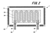
- 2 is a cross-sectional view taken along line AA shown in FIG. 1.
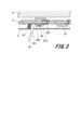
- 3 is a cross-sectional view showing an electrical connection relationship between a GND pattern and a housing in the first embodiment of the present invention.
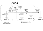
- FIG. FIG. 1 is an equivalent circuit diagram showing a human body model and an electronic control device model in an electrostatic discharge test for in-vehicle devices.
- 1 is an equivalent circuit diagram showing a state in which the charge on the housing is removed after static electricity is applied in an electrostatic discharge test for in-vehicle devices.
- FIG. 2 is a cross-sectional view taken along line BB shown in FIG. 1.
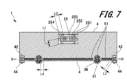
- FIG. 7 is a cross-sectional view taken along line CC shown in FIG. 6.
- 2 is a cross-sectional view taken along line DD shown in FIG. 1.
- 9 is a cross-sectional view taken along line EE shown in FIG. 8.
- 9 is a cross-sectional view taken along line FF shown in FIG. 8.
- 5 is a vertical cross-sectional view of an electronic control device according to a second embodiment of the present invention.
- 13 is a cross-sectional view showing an electrical connection relationship between a GND pattern and a conductive internal member according to a modified example of the second embodiment of the present invention.
- FIG. 11 is a vertical cross-sectional view of an electronic control device according to a third embodiment of the present invention.
- 11 is a vertical cross-sectional view of an electronic control device according to a fourth embodiment of the present invention.
- FIG. Fig. 1 is a vertical cross-sectional view of an electronic control device according to a first embodiment of the present invention
- Fig. 2 is a schematic cross-sectional view taken along line AA shown in Fig. 1.
- the electronic control device 1 is, for example, an electronic control device mounted on a vehicle that runs on liquid fuel such as gasoline or diesel.
- the electronic control device according to the present invention can also be widely applied to electronic control devices mounted on vehicles such as vehicles that run on hydrogen as fuel, hybrid type vehicles, and electric vehicles.
- the object controlled by the electronic control device is not limited to a specific object.
- the electronic control device 1 includes multiple printed circuit boards 2, a conductive internal member 3, and a housing 4.
- the printed circuit board 2 is composed of a plurality of electronic components 21, a pattern 22, a substrate 24, and a connector 25.
- the plurality of electronic components 21 are integrated circuits (ICs), resistors, capacitors, etc.
- the plurality of electronic components 21 are electrically connected to the pattern 22 by soldering or the like to form an electronic circuit.
- the electronic circuit realizes the control function required for the electronic control device 1. Note that the number of electronic components 21 may be one.
- Pattern 22 functions as wiring for an electronic circuit.
- Pattern 22 is formed by dividing a thin conductive film such as copper foil into multiple parts using etching or other processes.
- Pattern 22 can be composed of multiple layers overlapping in the thickness direction. Pattern 22 can also be formed not only on the surface of substrate 24 but also inside substrate 24.
- FIG. 1 shows an example of forming a pattern 22 consisting of two layers provided on both sides of a substrate 24.
- the patterns 22 in the two layers are electrically connected by conductive vias 23. This allows the pattern 22 to function as a single wiring, realizing a three-dimensional, complex circuit.
- the GND pattern 221 which is assigned to the ground potential, which is the reference potential of the electronic circuit.
- the ground potential is referenced at various points within the electronic circuit. However, if the potential difference between multiple ground potentials is not small enough, it may cause malfunctions of the electronic circuit.
- the total area of the GND pattern 221 is generally the largest compared to the points in pattern 22 assigned to other potentials.
- the substrate 24 is a plate or film made of an insulating material such as glass epoxy resin.
- the substrate 24 mechanically supports the multiple electronic components 21 and patterns 22.
- the connector 25 electrically connects the pattern 22 to an external wire harness (not shown). This allows the electronic control device 1 to input and output signals between the electronic control device 1 and external devices such as sensors and actuators.
- the conductive internal member 3 is made of metal or conductive resin.
- a plurality of printed circuit boards 2 are attached to the conductive internal member 3 using bolts 31 and spacers 32. Note that, instead of the bolts 31, rivets (not shown) may be used to attach the plurality of printed circuit boards 2.
- the conductive internal member 3 can be made of a material with high thermal conductivity, such as aluminum. In this case, the conductive internal member 3 and the multiple electronic components 21 are in contact with each other and thermally coupled to each other. This allows the heat generated by the multiple electronic components 21 to be effectively dissipated.
- a flow path 33 is formed inside the conductive internal member 3.
- a fluid 34 such as a coolant, circulates through the flow path 33. Heat generated in the multiple electronic components 21 is transferred to an external cooling device (not shown) through the fluid 34. This allows the conductive internal member 3 to exhibit high heat dissipation capabilities.
- the flow path 33 is formed so as to meander inside the conductive internal member 3. This allows the surface area of the flow path 33 to be maximized, and allows heat to be effectively transferred from the conductive internal member 3 to the fluid 34.
- Pipes 35 made of an insulating material such as resin are inserted into both ends of the flow path 33.
- Bases 36 made of a conductor such as metal are inserted into the pipes 35.
- the bases 36 are connected to external pipes (not shown) that are connected to an external cooling device.
- the conductive internal member 3 may be molded, for example, as two parts that face each other in the vertical direction, and then assembled.
- the housing 4 of this embodiment is constructed by molding two parts that face each other in the vertical direction, and combining these two parts with a conductive gasket 51 in between.
- the gasket 51 is made from a conductive foam material or a metal spring material, and is both conductive and flexible. The gasket 51 electrically connects the two parts of the housing 4.
- the housing 4 has a support 41 that supports the conductive internal member 3.
- the housing 4 surrounds the printed circuit board 2 and the conductive internal member 3 in three dimensions. This makes it possible to protect the printed circuit board 2 from external foreign objects, and to prevent short circuits in the electronic circuit caused by foreign objects.
- the housing 4 can also function as a shield for the printed circuit board 2. The structure of this shield will be described later.
- FIG. 3 is a cross-sectional view showing the electrical connection relationship between the GND pattern and the housing 4 in the first embodiment.
- the GND pattern 221 is connected to the housing 4 through a resistor 52, a frame ground pattern 222, and a gasket 51. Since the resistor 52 is provided between the housing 4 and the GND pattern 221, the GND pattern 221 and the housing 4 are electrically isolated.
- FIG. 4 is an equivalent circuit diagram showing a human body model and an electronic control device model in an electrostatic discharge test for in-vehicle devices.
- the form of electrostatic surge that should be considered in the electronic control device 1 varies depending on the field and application of use.
- the International Organization for Standardization (ISO) Road vehicles - Test methods for electrical disturbances from electrostatic discharge shows a "human body model" consisting of a static electricity storage capacity of 330 picofarads and a discharge resistance of 330 ohms as a model of the source of static electricity.
- the static electricity storage capacitance is Cd and the discharge resistance is Rd.
- the model on the electronic control device 1 side is represented by the capacitance Cc of the housing 4 with respect to the vehicle body earth and the isolation resistance Rs.
- the surge current Is caused by static electricity flows from the static electricity storage capacitance Cd through the discharge resistance Rd to the housing 4.
- the surge current Is flows from the housing 4 mainly through the isolation resistance Rs to the GND pattern 221.
- the surge current Is then finally returns to the vehicle body earth through the wire harness.
- the value of the isolation resistance Rs should be set to 3 kiloohms or more. Note that in this calculation, the capacitance Cc of the housing 4 is set to 0 picofarads, and the impedance of the wire harness is set to 0 ohms.
- FIG. 5 is an equivalent circuit diagram showing a case where the charge on the case is removed after static electricity is applied in an electrostatic discharge test for in-vehicle devices.
- the resistance value of resistor 52 is made too large, another problem becomes apparent. Therefore, the upper limit of the resistance value of resistor 52 must also be considered.
- the other problem is the charging of the housing 4. If the GND pattern 221 and the housing 4 are completely insulated, when the housing 4 becomes charged due to a surge 61 such as static electricity, there is no path for the charge to escape. Therefore, the housing 4 will remain charged for a long time. As a result, the housing 4 will attract dust and dirt. Therefore, it is necessary to remove the charge that has built up on the housing 4 in a short time.
- the static elimination time constant Tn which determines the time required to eliminate static electricity from the housing 4, is determined by the product of the capacitance Cc of the housing 4 and the separation resistance Rs shown in FIG. 5. The time required to eliminate the charge stored in the housing 4 in the electronic control device 1 is set according to the field and application of use.
- the value of the capacitance Cc of the housing 4 is required.
- the value of the capacitance Cc differs depending on the structure of the individual electronic control device 1. For example, if the housing 4 is modeled as a conductive sphere of diameter D isolated in the air, the capacitance Cc is expressed by the following formula (1) using the circular constant ⁇ and the dielectric constant of air ⁇ .
- the capacitance Cc is approximately 10 picofarads.
- the upper limit of the isolation resistance Rs can be designed to be 100 megaohms by dividing 1 millisecond by 10 picofarads. From the above explanation, it is preferable to set the isolation resistance value Rs to be greater than or equal to 3 kiloohms and less than or equal to 100 megaohms.
- FIG. 6 is a schematic diagram of a cross section taken along line BB shown in FIG.
- the housing 4 has a shielding structure 43 that three-dimensionally surrounds the printed circuit board 2 and the conductive internal member 3. This makes it possible to attenuate external noise 62 received from other electronic control devices 11 outside the electronic control device 1. It also makes it possible to attenuate radiated noise (not shown) emitted by multiple electronic components 21 inside the electronic control device 1. As a result, it is possible to improve the EMC performance between the electronic control devices 1 and 11, and to suppress the occurrence of malfunctions of the electronic control devices 1 and 11.
- FIG. 7 is a schematic diagram of a cross section taken along line CC shown in FIG.
- the housing 4 cannot completely surround the printed circuit board 2 and the conductive internal members 3 in three dimensions without any gaps. Therefore, gaps will be created in the housing 4 that connect the inside to the outside.
- the electronic control device 1 needs to input and output signals from external devices such as sensors and actuators. Therefore, gaps will be created around and inside the connector 25 that is provided to electrically connect to the external device.
- the connector 25 has a plurality of signal pins 251 for transmitting signals, a frame ground pin 252, a conductive shell 253, and a spring-like shell gasket 254.
- the frame ground pin 252 is electrically connected to the frame ground pattern 222 (see FIG. 3).
- the shell 253 is formed in a housing shape that houses multiple signal pins 251.
- the shell 253 has an opening that exposes one end of the multiple signal pins 251.
- the shell 253 is also electrically connected to the frame ground pattern 222 (see FIG. 3).
- the shell gasket 254 is in contact with the housing 4 and the shell 253. As a result, the shell gasket 254 provides electrical conductivity between the housing 4 and the shell 253.
- the size of the gap in the shield structure 43 is represented by the diagonal length of the largest gap in the connector 25.
- the diagonal length of the gap surrounded by the shell 253, shell gasket 254, and housing 4 is L1
- the diagonal length of the gap surrounded by the frame ground pin 252 and shell 253 is L2.
- the diagonal length of the gap that cannot be filled by the gasket 51 between the upper and lower parts that make up the housing 4 and the bolts 42 and nuts 44 that fasten them is L3.
- the diagonal length of the gap that cannot be filled by the gasket 51 between the upper and lower parts that make up the housing 4 and the base 36 is L4.
- the size of the gap in the shield structure 43 is represented by the longest of the diagonal lengths L1 to L4.
- the frequency of electromagnetic noise that should be considered in the electronic control device 1 varies depending on the field and application in which it is used.
- "Vehicles, boats and internal combustion engines - Radio disturbance characteristics - Limits and methods of measurement for the protection of on-board receivers” states that electromagnetic waves with frequencies up to 2.5 GHz should be considered as radiated interference waves.
- the wavelength of 2.5 GHz electromagnetic waves in air is approximately 120 millimeters. Therefore, to obtain a shielding effect of 20 dB or more against electromagnetic waves up to 2.5 GHz, the diagonal length L of the largest gap should be 6 millimeters or less.
- FIGS. Fig. 8 is a cross-sectional view taken along line DD shown in Fig. 1.
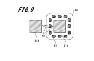
- Fig. 9 is a cross-sectional view taken along line EE shown in Fig. 8.
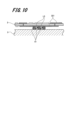
- Fig. 10 is a cross-sectional view taken along line FF shown in Fig. 8.
- the GND pattern 221 is electrically connected (conductive) to the conductive internal member 3 through the gasket 51.
- the GND pattern 221, the conductive internal member 3, and the gasket 51 form an electronic component shielding structure 63 that three-dimensionally surrounds the electronic component 211 of the multiple electronic components 21.
- the electronic component shielding structure 63 may also surround multiple electronic components three-dimensionally.
- the electronic component shielding structure 63 can attenuate external noise 62 emitted from other electronic components 212 around the electronic component 211.
- the electronic component shielding structure 63 can also attenuate radiation noise (not shown) emitted by the electronic component 211. This can improve the EMC performance between the electronic components 211 and 212. As a result, malfunction of the electronic circuit can be suppressed.
- the size of the gap in the electronic component shielding structure 63 is such that the diagonal length L5 (see FIG. 10) of the largest gap is 6 millimeters or less.
- the resistor 52 is used to electrically isolate the GND pattern 221 from the housing 4.
- the electrical isolation between the GND pattern and the housing according to the present invention may also be achieved by, for example, forming the support 41 interposed between the conductive internal member 3 and the housing 4 from a weakly conductive resin. This allows the GND pattern 221 and the housing 4 to be electrically isolated with an appropriate resistance value (3 kilohms or more and 100 megahms or less) without using the resistor 52.
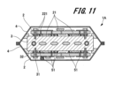
- FIG. 11 is a vertical cross-sectional view of an electronic control device according to the second embodiment.
- the electronic control device 1A according to the second embodiment has a similar configuration to the electronic control device 1 according to the first embodiment (see FIG. 1).
- the electronic control device 1A differs from the electronic control device 1 mainly in the number of gaskets 51. Therefore, here, differences from the first embodiment, such as the position where the gaskets 51 are provided, will be described, and descriptions of parts that overlap with those of the first embodiment will be omitted.
- the number of gaskets 51 interposed between the GND pattern 221 and the conductive internal member 3 of the electronic control device 1A is greater than that of the electronic control device 1.
- the bolts 31 and spacers 32 that mechanically fix the printed circuit board 2 to the conductive internal member 3 are formed of a conductive material such as metal.
- the GND pattern 221 is disposed at the location where the bolts 31 and spacers 32 contact the printed circuit board 2. Note that conductive rivets (not shown) may be used instead of the bolts 31.
- the electronic control device 1A not only the GND pattern 221 but also the conductive internal member 3 is used as the ground. Specifically, the GND pattern 221 and the conductive internal member 3 are electrically connected via a number of gaskets 51, bolts 31, and spacers 32.
- the electronic control device 1A can reduce the potential difference between the ground potentials referenced at various points on the printed circuit board 2. This can prevent malfunctions in electronic circuits.
- FIG. 12 is a cross-sectional view showing an electrical connection relationship between a GND pattern and a conductive internal member according to a modification of the second embodiment.
- a modified conductive internal member 3 has a boss portion 37 at the portion where the bolt 31 is screwed. This allows the spacer 32 to be omitted.
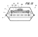
- FIG. 13 is a vertical cross-sectional view of an electronic control device according to the third embodiment.
- the electronic control device 1B according to the third embodiment has a similar configuration to the electronic control device 1 according to the first embodiment (see FIG. 1).
- the electronic control device 1B differs from the electronic control device 1 mainly in that there is only one printed circuit board 2 and in the electrical connection between the frame ground pattern 222 and the housing 4. Therefore, here, only the differences from the first embodiment will be described, and a description of parts that overlap with those of the first embodiment will be omitted.
- the electronic control device 1B includes a printed circuit board 2, a conductive internal member 3, and a housing 4.
- the frame ground pattern 222 of the electronic control device 1B is electrically connected to the housing 4 via the shell 253 and the shell gasket 254.
- the frame ground pattern 222 in the third embodiment is electrically connected to the housing 4 without the gasket 51.
- the electronic control device 1B can also ensure surge resistance and noise EMC performance.
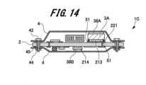
- FIG. 14 is a vertical cross-sectional view of an electronic control device according to the fourth embodiment.
- the electronic control device 1C according to the fourth embodiment has a similar configuration to the electronic control device 1 according to the first embodiment (see FIG. 1).
- the main differences between the electronic control device 1C and the electronic control device 1 are that there is only one printed circuit board 2 and a conductive internal member 3A. Therefore, only the differences from the first embodiment will be described here, and descriptions of parts that overlap with those of the first embodiment will be omitted.
- the electronic control device 1C includes one printed circuit board 2, a conductive internal member 3A, and a housing 4.
- the printed circuit board 2 is sandwiched between the upper and lower components that make up the housing 4 via a spacer 45.
- the printed circuit board 2 and housing 4 are fastened together using a bolt 42 that passes through the spacer 45, housing 4, and printed circuit board 2, and a nut 44 that screws onto the bolt 42.
- the printed circuit board 2 is mechanically fixed to the housing 4.
- the conductive internal member 3A is made of metal or conductive resin. No flow path for circulating a fluid such as a coolant is formed inside the conductive internal member 3A.
- the conductive internal member 3A is in contact with and thermally coupled to at least one electronic component 213 of the multiple electronic components 21.
- the conductive internal member 3A is in contact with the thermally conductive sheet 38A.
- the thermally conductive sheet 38A is in contact with the inner surface of the housing 4. Therefore, the heat generated by the electronic component 213 is transferred to the conductive internal member 3A and the thermally conductive sheet 38A, and dissipated from the housing 4 to the outside air.
- another electronic component 214 of the multiple electronic components 21 is in contact with the thermally conductive sheet 38B.
- the thermally conductive sheet 38B is in contact with the inner surface of the housing 4. Therefore, the heat generated by the electronic component 214 is transferred to the thermally conductive sheet 38B and dissipated from the housing 4.
- the electronic control device 1C does not require the provision of flow paths or piping in the conductive internal member 3A, nor does it require an external cooling device. This allows the electronic control device 1C to reduce costs.
- the electronic control device 1C can also ensure surge resistance and noise EMC performance.
- the electronic control device 1 includes a printed circuit board 2 on which electronic components 21 and conductive patterns 22 are mounted, a conductive internal member 3 to which heat from the electronic components 21 is transferred, and a housing 4 that at least two-dimensionally surrounds the printed circuit board 2 and the conductive internal member 3.
- the GND pattern 221 which is the conductive pattern with the largest total area of the printed circuit board 2, is electrically connected to the conductive internal member 3 and is electrically isolated from the housing 4. This allows the housing 4 to function as a shield for the printed circuit board 2.
- the electronic control device 1 can improve the EMC performance between the electronic control device 1 and the external electronic control device 11. In addition, it is possible to prevent the potential disturbance 611 generated when the surge 61 is applied from being directly transmitted to the GND pattern 221. As a result, it is possible for the electronic control device 1 to ensure resistance to the surge 61.
- the conductive internal member 3 according to the first embodiment described above has the flow passage 33 therein for circulating the fluid 34 . This allows the conductive internal member 3 to exhibit high heat dissipation capability.
- the conductive gasket 51 is interposed between the GND pattern 221 and the conductive internal member 3 according to the first embodiment described above. This makes it possible to easily establish electrical continuity between the GND pattern 221 and the conductive internal member 3 .
- the electronic control device 1 includes the resistor 52 that electrically isolates the GND pattern 221 from the housing 4 . This makes it possible to easily electrically isolate the GND pattern 221 from the housing 4 .
- the resistance value of the resistor 52 according to the first embodiment described above is equal to or greater than 3 kilohms and equal to or less than 100 megahms. This makes it possible to suppress the value of the surge current Is and to suppress charging of the housing 4 .
- the housing 4 according to the first embodiment described above forms a shield structure that three-dimensionally surrounds the printed circuit board 2 . This makes it possible to protect the printed circuit board 2 from external foreign matter, and to prevent the foreign matter from causing a short circuit in the electronic circuit, etc. Also, the shielding function of the housing 4 can be improved.
- the diagonal length of the gap in the shield structure 43 according to the first embodiment described above is 6 millimeters or less. This makes it possible to obtain a shielding effect of 20 dB or more against electromagnetic waves up to 2.5 GHz.
- the conductor including the GND pattern 221 and the conductive internal member 3 according to the first embodiment described above constitutes an electronic component shield structure 63 that three-dimensionally surrounds some of the electronic components 211 .
- the diagonal length of the gap in the electronic component shielding structure 63 according to the first embodiment described above is 6 millimeters or less. This makes it possible to obtain a shielding effect of 20 dB or more against electromagnetic waves up to 2.5 GHz.
- the support body 41 is interposed between the conductive internal member 3 and the housing 4 according to the first embodiment described above. This makes it possible to electrically isolate the GND pattern 221 and the housing 4 with an appropriate resistance value (not less than 3 kilohms and not more than 100 megahms) without using a resistor 52 .
- the GND pattern 221 according to the second embodiment described above is electrically connected to the conductive internal member 3 at a plurality of points. This makes it possible to reduce the potential difference between the ground potentials provided at various points on the printed circuit board 2. As a result, it is possible to suppress the occurrence of malfunctions of electronic circuits.
- the printed circuit board 2 according to the second embodiment described above is fixed to the conductive internal member 3 by using a conductive bolt 31 or a rivet.
- the GND pattern 221 is disposed at a location where the bolt 31 or the rivet contacts the printed circuit board 2. This makes it possible to easily establish electrical continuity between the GND pattern 221 and the conductive internal member 3 .
- the electronic control device 1 includes a printed circuit board 2 on which electronic components 21 and conductive patterns 22 are mounted, a conductive internal member 3 to which heat from the electronic components 21 is transferred, and a housing 4 that at least two-dimensionally surrounds the printed circuit board 2 and the conductive internal member 3.
- a GND pattern 221 which is a conductive pattern on the printed circuit board 2 to which a reference potential is assigned, is electrically connected to the conductive internal member 3 and is electrically isolated from the housing 4. This allows the housing 4 to function as a shield for the printed circuit board 2.
- the electronic control device 1 can improve the EMC performance between the electronic control device 1 and the external electronic control device 11. In addition, it is possible to prevent the potential disturbance 611 generated when the surge 61 is applied from being directly transmitted to the GND pattern 221. As a result, it is possible for the electronic control device 1 to ensure resistance to the surge 61.
Landscapes
- Engineering & Computer Science (AREA)
- Microelectronics & Electronic Packaging (AREA)
- Physics & Mathematics (AREA)
- Thermal Sciences (AREA)
- Shielding Devices Or Components To Electric Or Magnetic Fields (AREA)
Abstract
本発明は、サージの耐性とノイズのEMC性能の確保を実現する。電子制御装置は、電子部品と導電性のパターンとが実装されたプリント基板と、電子部品の熱が伝わる導電性内部部材と、プリント基板及び導電性内部部材を少なくとも二次元的に囲う筐体とを備える。プリント基板の最も合計面積が大きい導電性のパターンであるGNDパターンは、導電性内部部材と導通しており、筐体と電気的に分離されている。
Description
本発明は、電子制御装置に関する。
従来から、自動車に代表される輸送機器などにおいて、所望の制御を実現するために電子制御装置が用いられている。電子制御装置は、制御対象に取り付けられたセンサもしくは他の装置から入力される信号をもとに制御演算などの電子的な処理を行う。そして、電子制御装置は、処理結果を制御対象に取り付けられたアクチュエータもしくは他の装置へ出力する。このような電子制御装置は、機械的な制御装置と比べて柔軟且つきめ細かい制御を実現することができ、機器全体で高い性能を発揮することができる。
一般的に電子制御装置は、マイコン(Micro Controller Unit)などの電子部品と銅箔などからなる導電性のパターンとが実装されたプリント基板と、それを機械的に保持する筐体とを備える。筐体は、プリント基板を三次元的に囲う構造となっていることが多い。これにより、筐体は、外部の異物からプリント基板を保護することができる。
筐体が金属などの熱伝導率が高い材料で形成されている場合は、電子部品と筐体とを熱的に接触させた構造とする場合がある。この場合は、電子部品で発生した熱を、筐体を通じて効率よく放熱することができる。さらに、筐体内部に流路を形成してそこに冷却液を循環させる、いわゆる水冷筐体とすることで、より高い放熱効果を得ることができる。
また、電子制御装置に複数のプリント基板が搭載される場合は、装置全体をコンパクトにするために基板同士を重ねる構造とすることがある。この構造に加えてさらに水冷筐体を用いる場合は、コストの高い水冷筐体をひとつにまとめる目的で、水冷筐体の上下にプリント基板を配置する。さらに、プリント基板の外側を別の筐体で囲む、二重筐体構造を採用することがある。
一般に、電子制御装置は、サージへの耐性とノイズへのEMC(electro-magnetic compatibility)性能の双方を必要なレベルで実現する必要がある。サージは、静電気などのエネルギーが大きい不要信号であり、そのエネルギーによって電子部品を破壊することがある。また、サージは、電子回路を構成する各配線の電位に擾乱を与え、電子回路に誤動作が発生することがある。そのため、電子制御装置は、想定される種類及びエネルギーの大きさのサージに対して十分な耐性を持つ必要がある。
ノイズは、外部の装置との電磁的な干渉、もしくは装置内の電子回路どうしの電磁的な干渉などによるエネルギーが小さい不要信号である。電子回路を構成する各配線の電位にノイズが重畳することで、電子回路の誤動作などが発生することがある。そのため、電子制御装置は、想定される種類及びエネルギーの大きさのノイズに対して十分な耐性を持つ必要がある。
また、電子回路は、動作している限り周囲に放出するノイズをゼロにすることはできない。そのため、電子制御装置は、ノイズの量を許容量よりも小さくする必要がある。EMC(電磁両立性)は、想定される外部からのノイズに対して十分な耐性を持たせ、且つ、自身が放出するノイズを許容量より小さくすることである。
サージへの耐性やノイズへのEMC性能を確保する方法としては、金属などの導電性の材料から形成された筐体とプリント基板上のパターンとの間の電気的な接続方式を工夫するものがある。プリント基板上のパターンとしては、特に電子回路の基準電位であるグラウンド電位に割り当てられたパターン(以下、「GNDパターン」とする)が用いられる。
電子制御装置の筐体とGNDパターンとを導通させ、且つ、筐体がプリント基板を三次元的に囲う構造とした場合に、筐体は、プリント基板のシールドとして機能する。これにより、外部から電子制御装置に入り込むノイズを減衰させることができ、また、電子制御装置内部の電子回路が放出するノイズを減衰させることができる。その結果、電子制御装置は、EMC性能を確保しやすくなる。
一方、筐体とGNDパターンとを電気的に分離すると、電子制御装置の外部から静電気などのサージが筐体に印加されたときに、そのサージがGNDパターンに直接伝達されない。したがって、グラウンド電位が受ける擾乱を小さくすることができ、電子回路の誤動作の発生を抑制することができる。
特許文献1には、外部ノイズが電子部品に及ぼす影響を抑制することができる電子機器が開示されている。特許文献1に開示された電子機器は、筐体とシグナルグランド(上述のGNDパターンに対応)とを絶縁して、外部ノイズ(上述のサージに対応)がシグナルグランドに伝達されることを防止している。
しかし、特許文献1に開示された電子機器では、外部ノイズ(上述のサージに対応)ジが電子部品(電子回路)に及ぼす影響を抑制することはできるが、筐体をプリント基板のシールドとして機能させることはできない。そのため、ノイズのEMC性能の確保を実現することができなかった。
本発明は、上記の点に鑑みてなされたものであり、サージの耐性とノイズのEMC性能の確保を実現することができる電子制御装置を提供することを目的とする。
上記課題を解決し、本発明の目的を達成するため、本発明の一態様である電子制御装置は、電子部品と導電性のパターンとが実装されたプリント基板と、電子部品の熱が伝わる導電性内部部材と、プリント基板及び導電性内部部材を少なくとも二次元的に囲う筐体とを備える。プリント基板の最も合計面積が大きい導電性のパターンであるGNDパターンは、導電性内部部材と導通しており、筐体と電気的に分離されている。
上記構成の電子制御装置によれば、サージの耐性とノイズのEMC性能の確保を実現することができる。
なお、上述した以外の課題、構成および効果は、以下の実施形態の説明により明らかにされる。
なお、上述した以外の課題、構成および効果は、以下の実施形態の説明により明らかにされる。
1.第1実施形態
以下、本発明の第1実施形態について図面を参照して詳細に説明する。本明細書および図面において、実質的に同一の機能または構成を有する要素については、同一の符号を付し、重複する説明は省略する。
以下、本発明の第1実施形態について図面を参照して詳細に説明する。本明細書および図面において、実質的に同一の機能または構成を有する要素については、同一の符号を付し、重複する説明は省略する。
[電子制御装置の構成]
まず、第1実施形態に係る電子制御装置の構成について、図1及び図2を用いて説明する。
図1は、第1実施形態に係る電子制御装置の縦断面である。図2は、図1に示すA-A線に沿う断面の模式図である。
まず、第1実施形態に係る電子制御装置の構成について、図1及び図2を用いて説明する。
図1は、第1実施形態に係る電子制御装置の縦断面である。図2は、図1に示すA-A線に沿う断面の模式図である。
電子制御装置1は、例えば、ガソリンや軽油などの液体燃料を用いて走行する車両に搭載される電子制御装置である。本発明に係る電子制御装置は、例えば、水素を燃料に用いて走行する車両、ハイブリッドタイプの車両、電気自動車などの車両に搭載される電子制御装置にも広く適用可能である。また、電子制御装置が制御する対象物は、特定の対象物に限定されるものではない。
図1及び図2に示すように、電子制御装置1は、複数のプリント基板2と、導電性内部部材3と、筐体4とを備えている。
(プリント基板の構成)
プリント基板2は、複数の電子部品21、パターン22、基材24、およびコネクタ25から構成される。複数の電子部品21は、集積回路(IC)や抵抗器、コンデンサなどである。複数の電子部品21は、はんだ付けなどによりパターン22に電気的に接続されることで電子回路を構成する。電子回路は、電子制御装置1に求められる制御機能を実現する。なお、電子部品21は1つであってもよい。
プリント基板2は、複数の電子部品21、パターン22、基材24、およびコネクタ25から構成される。複数の電子部品21は、集積回路(IC)や抵抗器、コンデンサなどである。複数の電子部品21は、はんだ付けなどによりパターン22に電気的に接続されることで電子回路を構成する。電子回路は、電子制御装置1に求められる制御機能を実現する。なお、電子部品21は1つであってもよい。
パターン22は、電子回路の配線として機能する。パターン22は、銅箔などの導電性の薄膜をエッチング加工などで複数の部位に分割することで形成されている。パターン22は、厚み方向に重なる複数の層から構成するができる。また、パターン22は、基材24の表面だけでなく基材24の内部に形成することもできる。
図1は、基材24の両面に設けられた2つの層からなるパターン22を形成した例を示している。2つの層におけるパターン22は、導電性のビア23によって電気的に接続されている。これにより、パターン22を1つの配線として機能させることができ、立体的で複雑な回路を実現することができる。
このように電気的に接続されたパターン22のうち、最も重要なのは、電子回路の基準電位であるグラウンド電位に割り当てられたGNDパターン221である。グラウンド電位は、電子回路内の様々な箇所で参照される。しかし、複数のグラウンド電位の電位差が十分に小さくなければ、電子回路の誤動作などを引き起こすおそれがある。
複数のグラウンド電位間の電位差を低く保つには、グラウンド電位が参照されるすべての箇所の間を低い抵抗値で電気的に接続する必要がある。これを実現するには、GNDパターン221の幅をできるだけ太くしてプリント基板2の隅々まで張り巡らし、さらに複数の層を使ってそれらの間を多数のビア23で接続することが有効である。したがって、GNDパターン221は、パターン22のうちの他の電位に割り当てられた箇所と比べて、合計面積が最も大きくなることが一般的である。
基材24は、ガラスエポキシ樹脂などの絶縁体からなる板体またはフィルムである。基材24は、複数の電子部品21やパターン22を機械的に支持する。
コネクタ25は、パターン22と外部のワイヤーハーネス(図示しない)とを電気的に接続する。これにより、電子制御装置1は、外部のセンサやアクチュエータなどの装置との間で信号の入出力を実現する。
(導電性内部部材の構成)
導電性内部部材3は、金属や導電性樹脂から形成されている。導電性内部部材3には、複数のプリント基板2がボルト31及びスペーサー32を用いて取り付けられている。なお、複数のプリント基板2の取り付けには、ボルト31に代えて、リベット(図示しない)を用いてもよい。
導電性内部部材3は、金属や導電性樹脂から形成されている。導電性内部部材3には、複数のプリント基板2がボルト31及びスペーサー32を用いて取り付けられている。なお、複数のプリント基板2の取り付けには、ボルト31に代えて、リベット(図示しない)を用いてもよい。
(導電性内部部材による放熱)
導電性内部部材3は、アルミニウムなどの熱伝導性が高い材料で作ることができる。その場合は、導電性内部部材3と複数の電子部品21を接触させて熱的に結合した構成とする。これにより、複数の電子部品21で発生した熱を効果的に放熱させることができる。
導電性内部部材3は、アルミニウムなどの熱伝導性が高い材料で作ることができる。その場合は、導電性内部部材3と複数の電子部品21を接触させて熱的に結合した構成とする。これにより、複数の電子部品21で発生した熱を効果的に放熱させることができる。
導電性内部部材3の内部には、流路33が形成されている。流路33の中には、冷却液などの流体34が循環されている。複数の電子部品21で発生した熱は、流体34を通じて外部の冷却装置(図示しない)に伝達される。これにより、導電性内部部材3は、高い放熱能力を発揮することができる。
図2に示すように、流路33は、導電性内部部材3の内部を蛇行するように形成されている。これにより、流路33の表面積をできるだけ大きくすることができ、導電性内部部材3から流体34へ効果的に熱を伝えることができる。
流路33の両端には、樹脂などの絶縁体からなる配管35がそれぞれ挿入されている。配管35には、金属などの導電体からなる口金36がそれぞれ挿入されている。口金36は、外部の冷却装置に接続された外部配管(図示しない)と接続されている。流路33と口金36との間に配管35が介在することで、導電性内部部材3と口金36とを電気的に分離することができる。
なお、流路33を含めた導電性内部部材3の構造を一体成形で実現すると、コストが高くなる場合がある。そのため、導電性内部部材3は、例えば、上下方向に対向する2つの部品に分けて成型し、組み立てる構造にしてもよい。
(筐体の構成)
筐体4は、金属や導電性樹脂から形成されている。筐体4は、プリント基板2及び導電性内部部材3を少なくとも二次元的に囲う構造となっている。これにより、電子制御装置1の運搬や車両への組み込み、および車両の整備などの際にプリント基板2を車両構造や工具などとの接触から保護することができる。
筐体4は、金属や導電性樹脂から形成されている。筐体4は、プリント基板2及び導電性内部部材3を少なくとも二次元的に囲う構造となっている。これにより、電子制御装置1の運搬や車両への組み込み、および車両の整備などの際にプリント基板2を車両構造や工具などとの接触から保護することができる。
筐体4を一体成形で実現すると、コストが高くなる場合がある。そのため、本実施形態の筐体4は、上下方向に対向する2つの部品を成型し、それら2つの部品を導電性のガスケット51を挟んで組み合わせる構造を採用している。ガスケット51は、導電性の発泡材や金属のばね材などから形成されており、導電性と柔軟性とを併せ持つ。ガスケット51は、筐体4の2つの部品間を電気的に接続する。
筐体4は、導電性内部部材3を支持する支持体41を有している。筐体4は、プリント基板2及び導電性内部部材3を三次元的に囲う。これにより、プリント基板2を外部の異物から保護することができ、異物により電子回路が短絡などを起こすことを防ぐことができる。また、筐体4をプリント基板2のシールドとして機能させることができる。このシールドの構造については後述する。
[GNDパターンと筐体との間の電気的な接続関係]
次に、GNDパターン221と筐体4との間の電気的な接続関係について、図3を使用して説明する。
図3は、第1実施形態におけるGNDパターンと筐体4との間の電気的な接続関係を示した断面図である。
次に、GNDパターン221と筐体4との間の電気的な接続関係について、図3を使用して説明する。
図3は、第1実施形態におけるGNDパターンと筐体4との間の電気的な接続関係を示した断面図である。
図3に示すように、GNDパターン221は、抵抗器52、フレームグラウンドパターン222、及びガスケット51を通じて筐体4に接続されている。筐体4とGNDパターン221との間に抵抗器52を設けたため、GNDパターン221と筐体4とは、電気的に分離されている。
筐体4の外から静電気などのサージ61が印加されると、電位の擾乱611が生じる。このとき、所定の抵抗値である抵抗器52を設けているため、電位の擾乱611がGNDパターン221に直接伝達されることを防ぐことができる。すなわち、GNDパターン221の電位であるグラウンド電位が受ける擾乱612を小さくして、サージ61の耐性を確保することができる。その結果、電子回路の誤動作の発生を抑制することができる。
[分断抵抗値の下限]
次に、抵抗器52における具体的な抵抗値の下限の一例について、図4を用いて説明する。
図4は、車載機器向けの静電気放電試験における人体モデルと電子制御装置モデルを示した等価回路図である。
次に、抵抗器52における具体的な抵抗値の下限の一例について、図4を用いて説明する。
図4は、車載機器向けの静電気放電試験における人体モデルと電子制御装置モデルを示した等価回路図である。
電子制御装置1において考慮すべき静電気サージの形態は、使用される分野や用途によって様々である。例えば、Road vehicles - Test methods for electrical disturbances from electrostatic discharge(ISO10605:2008)国際標準化機構(ISO)には、静電気の発生源のモデルとして、330ピコファラドの静電気蓄積容量と330オームの放電抵抗からなる「人体モデル」が示されている。
図4では、静電気蓄積容量をCd、放電抵抗をRdとする。また、電子制御装置1側のモデルを、筐体4の車体アースに対する静電容量Ccと分離抵抗Rsで表す。この場合に、静電気によるサージ電流Isは、静電気蓄積容量Cdから放電抵抗Rdを通じて筐体4に流れる。さらに、サージ電流Isは、筐体4から主に分離抵抗Rsを通じてGNDパターン221に流れる。そして、サージ電流Isは、最終的にワイヤーハーネスを通じて車体アースに戻る。
このとき、GNDパターン221と筐体4とを電気的に分離しない(Rs=0オーム)場合と比べて、サージ電流Isの値を1/10以下に抑えるには、分離抵抗Rsの値を3キロオーム以上にすればよい。なお、この計算において、筐体4の静電容量Ccを0ピコファラド、ワイヤーハーネスのインピーダンスを0オームとしている。
[分断抵抗値の上限]
次に、抵抗器52における具体的な抵抗値の上限の一例について、図5を用いて説明する。
図5は、車載機器向けの静電気放電試験において静電気印加後に筐体に帯電した電荷が除電されるときの等価回路図である。
次に、抵抗器52における具体的な抵抗値の上限の一例について、図5を用いて説明する。
図5は、車載機器向けの静電気放電試験において静電気印加後に筐体に帯電した電荷が除電されるときの等価回路図である。
抵抗器52の抵抗値をむやみに大きくすると、別の問題が顕在化する。そのため、抵抗器52の抵抗値については、上限も考慮する必要がある。別の問題とは、筐体4の帯電である。GNDパターン221と筐体4とを完全に絶縁していると、静電気などのサージ61により筐体4が帯電した場合に、電荷を逃がす経路がない。したがって、筐体4が長時間帯電し続けることになる。その結果、筐体4は、塵や埃を吸着してしまう。そこで、筐体4に帯電した電荷を短い時間で除電する必要がある。
筐体4の除電に要する時間を決める除電時定数Tnは、図5に示す筐体4の静電容量Ccの値と分離抵抗Rsの値との積で定まる。電子制御装置1において筐体4に帯電した電荷を除電する時間は、使用される分野や用途に応じて設定される。
例えば、「Road vehicles - Test methods for electrical disturbances from electrostatic discharge」((ISO10605:2008)国際標準化機構(ISO))には、静電気が印加される時間間隔が最短で1秒間と記載されている。そこで、除電時定数Tnの値を、静電気が印加される時間間隔より十分に短い時間、例えば1ミリ秒以下にすると、筐体4に対する塵や埃の吸着を抑制することができる。
除電時定数Tnの目標値から分離抵抗Rsの値を設計するには、筐体4の静電容量Ccの値が必要である。静電容量Ccの値は、個々の電子制御装置1の構造によって異なる。例えば、筐体4を空中に孤立した直径Dの導体球としてモデル化すると、静電容量Ccは、円周率πと空気の誘電率εを用いた次の式(1)で表される。
[数1]
Cc=2πεD…(1)
Cc=2πεD…(1)
直径Dを9センチメートルとすると、静電容量Ccは、約10ピコファラドとなる。ここから、分離抵抗Rsの上限値は、1ミリ秒を10ピコファラドで除算して、100メガオームと設計することができる。以上の説明から、分離抵抗値Rsの値は、3キロオーム以上100メガオーム以下に設定することが好適である。
[筐体によるシールド構造]
次に、筐体4によるシールド構造について、図6を用いて説明する。
図6は、図1に示すB-B線に沿う断面の模式図である。
次に、筐体4によるシールド構造について、図6を用いて説明する。
図6は、図1に示すB-B線に沿う断面の模式図である。
図6に示すように、筐体4は、プリント基板2及び導電性内部部材3を三次元的に囲うシールド構造43である。これにより、電子制御装置1の外部にある他の電子制御装置11から受ける外来ノイズ62を減衰させることができる。また、電子制御装置1内の複数の電子部品21が放出する放射ノイズ(不図示)を減衰させることができる。その結果、電子制御装置1,11間におけるEMC性能を向上させることができ、電子制御装置1,11の誤動作の発生を抑制することができる。
[シールド構造の隙間とその許容値]
次に、シールド構造43の隙間とその許容値について、図7を用いて説明する。
図7は、図2に示すC-C線に沿う断面の模式図である。
次に、シールド構造43の隙間とその許容値について、図7を用いて説明する。
図7は、図2に示すC-C線に沿う断面の模式図である。
筐体4は、プリント基板2及び導電性内部部材3を完全に隙間なく三次元的に囲うことはできない。したがって、筐体4には、内部と外部を連通させる隙間が生じる。前述したように、電子制御装置1は、センサやアクチュエータなどの外部装置と信号の入出力を行う必要がある。そのため、外部装置と電気的に接続させるために設けたコネクタ25の周囲及びその内部に隙間が生じる。
図7に示すように、コネクタ25は、信号を伝達するための複数の信号ピン251と、フレームグラウンドピン252と、導電性のシェル253と、ばね状のシェルガスケット254とを有している。フレームグラウンドピン252は、フレームグラウンドパターン222(図3参照)に電気的に接続されている。
シェル253は、複数の信号ピン251を収容する筐体状に形成されている。シェル253は、複数の信号ピン251の一端を露出させる開口部を有している。また、シェル253は、フレームグラウンドパターン222(図3参照)に電気的に接続されている。シェルガスケット254は、筐体4とシェル253に接触している。これにより、シェルガスケット254は、筐体4とシェル253との間を導通させている。
シールド構造43の隙間の大きさは、コネクタ25における最も大きい隙間の対角線長で代表される。ここで、シェル253、シェルガスケット254及び筐体4で囲まれた隙間の対角線長をL1として、フレームグラウンドピン252とシェル253とで囲まれた隙間の対角線長をL2とする。また、筐体4を構成する上下の部品とそれらを締結しているボルト42とナット44との間におけるガスケット51で塞ぎきれない隙間の対角線長をL3とする。そして、筐体4を構成する上下の部品と口金36との間におけるガスケット51で塞ぎきれない隙間の対角線長をL4とする。この場合に、シールド構造43の隙間の大きさは、対角線長L1~L4のうちの最も長いもので代表される。
次に、どの程度の大きさの隙間であれば許容できるかについて説明する。「電子機器・装置のノイズ対策入門」(p.142、斉藤成一著、オーム社出版)には、シールドにおいて20dBのシールド効果を得るには、シールド構造の最も大きい隙間の対角線長を減衰させたい電磁波の波長の1/20に抑える必要がある、と記載されている。
電子制御装置1において考慮すべき電磁ノイズの周波数は、その使われる分野や用途によって様々である。車載用電子制御装置について、例えば、「Vehicles, boats and internal combustion engines - Radio disturbance characteristics - Limits and methods of measurement for the protection of on-board receivers」((CISPR25:2016)、国際無線障害特別委員会(CISPR))には、放射妨害波として2.5ギガヘルツまでの周波数の電磁波を考慮することが記載されている。2.5ギガヘルツの電磁波の空気中における波長は、約120ミリメートルである。そのため、2.5ギガヘルツまでの電磁波に対して20dB以上のシールド効果を得るには、最も大きい隙間の対角線長Lを6ミリメートル以下にすればよい。
[GNDパターンと導電性内部部材との間の電気的な接続関係]
次に、GNDパターン221と導電性内部部材3との間の電気的な接続関係について、図8~図10を用いて説明する。
図8は、図1に示すD-D線に沿う断面図である。図9は、図8に示すE-E線に沿う断面図である。図10は、図8に示すF-F線に沿う断面図である。
次に、GNDパターン221と導電性内部部材3との間の電気的な接続関係について、図8~図10を用いて説明する。
図8は、図1に示すD-D線に沿う断面図である。図9は、図8に示すE-E線に沿う断面図である。図10は、図8に示すF-F線に沿う断面図である。
図8~図10に示すように、GNDパターン221は、ガスケット51を通じて導電性内部部材3に電気的に接続されている(導通している)。そして、GNDパターン221、導電性内部部材3、及びガスケット51は、複数の電子部品21のうちの電子部品211を三次元的に囲う電子部品シールド構造63を構成している。なお、電子部品シールド構造63は、複数の電子部品を三次元的に囲うものであってもよい。
電子部品シールド構造63は、電子部品211の周囲にある他の電子部品212から放出された外来ノイズ62を減衰させることができる。また、電子部品シールド構造63は、電子部品211が放出する放射ノイズ(不図示)を減衰させることができる。これにより、電子部品211,212間におけるEMC性能を向上させることができる。その結果、電子回路の誤動作の発生を抑制することができる。なお、電子部品シールド構造63の隙間の大きさは、前述のシールド構造43と同様、最も大きい隙間の対角線長L5(図10参照)を6ミリメートル以下にすることが好ましい。
[電気的分離のための別の方式]
本実施形態では、GNDパターン221と筐体4とを電気的に分離するために抵抗器52を用いる例を示した。しかし、本発明に係るGNDパターンと筐体との電気的な分離は、例えば、導電性内部部材3と筐体4との間に介在されている支持体41を弱導電性の樹脂によって形成することで実現してもよい。これにより、抵抗器52を用いることなく、GNDパターン221と筐体4とを適切な抵抗値(3キロオーム以上100メガオーム以下)で電気的に分離することができる。
本実施形態では、GNDパターン221と筐体4とを電気的に分離するために抵抗器52を用いる例を示した。しかし、本発明に係るGNDパターンと筐体との電気的な分離は、例えば、導電性内部部材3と筐体4との間に介在されている支持体41を弱導電性の樹脂によって形成することで実現してもよい。これにより、抵抗器52を用いることなく、GNDパターン221と筐体4とを適切な抵抗値(3キロオーム以上100メガオーム以下)で電気的に分離することができる。
2.第2実施形態
次に、本発明の第2実施形態について図11を参照して説明する。
図11は、第2実施形態に係る電子制御装置の縦断面である。
次に、本発明の第2実施形態について図11を参照して説明する。
図11は、第2実施形態に係る電子制御装置の縦断面である。
[電子制御装置の構成]
第2実施形態に係る電子制御装置1Aは、第1実施形態に係る電子制御装置1(図1参照)と同様の構成を備えている。電子制御装置1Aが電子制御装置1と異なる点は、主にガスケット51の数である。そのため、ここでは、ガスケット51を設ける位置等の第1実施形態と異なる点について説明し、第1実施形態と重複する部品の説明を省略する。
第2実施形態に係る電子制御装置1Aは、第1実施形態に係る電子制御装置1(図1参照)と同様の構成を備えている。電子制御装置1Aが電子制御装置1と異なる点は、主にガスケット51の数である。そのため、ここでは、ガスケット51を設ける位置等の第1実施形態と異なる点について説明し、第1実施形態と重複する部品の説明を省略する。
図11に示すように、電子制御装置1AのGNDパターン221と導電性内部部材3との間に介在されているガスケット51の数は、電子制御装置1よりも多い。また、プリント基板2を導電性内部部材3に対して機械的に固定するボルト31及びスペーサー32は、金属などの導電性の材料で形成されている。さらに、ボルト31やスペーサー32がプリント基板2と接触する箇所に、GNDパターン221が配置されている。なお、ボルト31に代えて、導電性のリベット(図示しない)を用いてもよい。
前述したように、電子回路の誤動作の発生を抑制するには、グラウンド電位が参照されるすべての箇所の間を低い抵抗値で電気的に接続する必要がある。電子制御装置1Aでは、GNDパターン221だけでなく、導電性内部部材3も併せてグラウンドとして用いる。具体的には、GNDパターン221と導電性内部部材3とを多数のガスケット51、ボルト31及びスペーサー32を介して導通させる。
[抵抗値の低減策]
ガスケット51、ボルト31及びスペーサー32の個数は、多いほど導電性内部部材3との接触面積が増える。これにより、グラウンド電位が参照されるすべての箇所の間の抵抗値を低減することができる。また、ボルト31やスペーサー32、導電性内部部材3どうしの接触部に小さな凹凸を設けたり(不図示)、それらの間に菊座ワッシャー(不図示)を介在させたりすることにより、部材どうしを食い込ませることができる。これにより、接触部分の酸化膜などを突き破ることができ、ボルト31及びスペーサー32を経由した抵抗値をさらに低減することができる。
ガスケット51、ボルト31及びスペーサー32の個数は、多いほど導電性内部部材3との接触面積が増える。これにより、グラウンド電位が参照されるすべての箇所の間の抵抗値を低減することができる。また、ボルト31やスペーサー32、導電性内部部材3どうしの接触部に小さな凹凸を設けたり(不図示)、それらの間に菊座ワッシャー(不図示)を介在させたりすることにより、部材どうしを食い込ませることができる。これにより、接触部分の酸化膜などを突き破ることができ、ボルト31及びスペーサー32を経由した抵抗値をさらに低減することができる。
電子制御装置1Aは、プリント基板2上の各所で参照されるグラウンド電位の間の電位差を小さくすることができる。これにより、電子回路の誤動作の発生を抑制することができる。
[変形例]
次に、第2実施形態に係る導電性内部部材3の変形例について、図12を用いて説明する。
図12は、第2実施形態の変形例に係るGNDパターンと導電性内部部材との間の電気的な接続関係を示した断面図である。
次に、第2実施形態に係る導電性内部部材3の変形例について、図12を用いて説明する。
図12は、第2実施形態の変形例に係るGNDパターンと導電性内部部材との間の電気的な接続関係を示した断面図である。
図12に示すように、導電性内部部材3の変形例は、ボルト31が螺合される部分にボス部37を有している。これにより、スペーサー32を省略することができる。
3.第3実施形態
次に、本発明の第3実施形態について図13を参照して説明する。
図13は、第3実施形態に係る電子制御装置の縦断面である。
次に、本発明の第3実施形態について図13を参照して説明する。
図13は、第3実施形態に係る電子制御装置の縦断面である。
[電子制御装置の構成]
第3実施形態に係る電子制御装置1Bは、第1実施形態に係る電子制御装置1(図1参照)と同様の構成を備えている。電子制御装置1Bが電子制御装置1と異なる点は、主にプリント基板2が1つである点と、フレームグラウンドパターン222と筐体4との間の電気的な接続である。そのため、ここでは、第1実施形態と異なる点について説明し、第1実施形態と重複する部品の説明を省略する。
第3実施形態に係る電子制御装置1Bは、第1実施形態に係る電子制御装置1(図1参照)と同様の構成を備えている。電子制御装置1Bが電子制御装置1と異なる点は、主にプリント基板2が1つである点と、フレームグラウンドパターン222と筐体4との間の電気的な接続である。そのため、ここでは、第1実施形態と異なる点について説明し、第1実施形態と重複する部品の説明を省略する。
図13に示すように、電子制御装置1Bは、1つのプリント基板2と、導電性内部部材3と、筐体4とを備えている。
電子制御装置1Bのフレームグラウンドパターン222は、シェル253及びシェルガスケット254を介して筐体4と電気的に接続されている。すなわち、第3実施形態に係るフレームグラウンドパターン222は、ガスケット51を介さずに筐体4と電気的に接続されている。電子制御装置1Bにおいても、サージの耐性とノイズのEMC性能の確保を実現することができる。
4.第4実施形態
次に、本発明の第4実施形態について図14を参照して説明する。
図14は、第4実施形態に係る電子制御装置の縦断面である。
次に、本発明の第4実施形態について図14を参照して説明する。
図14は、第4実施形態に係る電子制御装置の縦断面である。
[電子制御装置の構成]
第4実施形態に係る電子制御装置1Cは、第1実施形態に係る電子制御装置1(図1参照)と同様の構成を備えている。電子制御装置1Cが電子制御装置1と異なる点は、主にプリント基板2が1つである点と、導電性内部部材3Aである。そのため、ここでは、第1実施形態と異なる点について説明し、第1実施形態と重複する部品の説明を省略する。
第4実施形態に係る電子制御装置1Cは、第1実施形態に係る電子制御装置1(図1参照)と同様の構成を備えている。電子制御装置1Cが電子制御装置1と異なる点は、主にプリント基板2が1つである点と、導電性内部部材3Aである。そのため、ここでは、第1実施形態と異なる点について説明し、第1実施形態と重複する部品の説明を省略する。
図14に示すように、電子制御装置1Cは、1つのプリント基板2と、導電性内部部材3Aと、筐体4とを備えている。
プリント基板2は、スペーサー45を介して筐体4を構成する上下の部品に挟まれている。プリント基板2と筐体4は、スペーサー45、筐体4及びプリント基板2を貫通するボルト42と、ボルト42に螺合するナット44を用いて締結されている。すなわち、プリント基板2は、筐体4に対して機械的に固定されている。
導電性内部部材3Aは、金属や導電性樹脂から形成されている。導電性内部部材3Aの内部には、冷却液などの流体を循環させる流路が形成されていない。導電性内部部材3Aは、複数の電子部品21のうちの少なくとも1つの電子部品213と接触して、熱的に結合している。
また、導電性内部部材3Aは、熱伝導シート38Aに接触している。そして、熱伝導シート38Aは、筐体4の内側の面に接触している。したがって、電子部品213で発生した熱は、導電性内部部材3A及び熱伝導シート38Aに伝達され、筐体4から外部の空気に放熱される。
また、複数の電子部品21のうちの他の電子部品214は、熱伝導シート38Bに接触している。そして、熱伝導シート38Bは、筐体4の内側の面に接触している。したがって、電子部品214で発生した熱は、熱伝導シート38Bに伝達され、筐体4から放熱される。
電子制御装置1Cは、導電性内部部材3Aに流路や配管を設ける必要が無く、また、外部に冷却装置を設ける必要が無い。これにより、電子制御装置1Cは、コストの削減を図ることができる。また、電子制御装置1Cにおいても、サージの耐性とノイズのEMC性能の確保を実現することができる。
5.まとめ
(1)上述した第1実施形態に係る電子制御装置1は、電子部品21と導電性のパターン22とが実装されたプリント基板2と、電子部品21の熱が伝わる導電性内部部材3と、プリント基板2及び導電性内部部材3を少なくとも二次元的に囲う筐体4とを備える。プリント基板2の最も合計面積が大きい導電性のパターンであるGNDパターン221は、導電性内部部材3と導通しており、筐体4と電気的に分離されている。
これにより、筐体4をプリント基板2のシールドとして機能させることができる。その結果、電子制御装置1の外部にある他の電子制御装置11から受ける外来ノイズ62と、電子制御装置1内の電子部品21が放出する放射ノイズを減衰させることができる。したがって、電子制御装置1は、外部にある電子制御装置11との間のEMC性能を向上させることができる。また、サージ61が印加されると生じる電位の擾乱611が、GNDパターン221に直接伝達されることを防ぐことができる。その結果、電子制御装置1は、サージ61の耐性を確保することができる。
(2)上述した第1実施形態に係る導電性内部部材3は、内部に流体34を循環させる流路33を有する。
これにより、導電性内部部材3は、高い放熱能力を発揮することができる。
これにより、導電性内部部材3は、高い放熱能力を発揮することができる。
(3)上述した第1実施形態に係るGNDパターン221と導電性内部部材3との間には、導電性のガスケット51が介在されている。
これにより、GNDパターン221と導電性内部部材3を容易に導通させることができる。
これにより、GNDパターン221と導電性内部部材3を容易に導通させることができる。
(4)上述した第1実施形態に係る電子制御装置1は、GNDパターン221と筐体4とを電気的に分離する抵抗器52を有する。
これにより、GNDパターン221と筐体4との電気的な分離を容易に行うことができる。
これにより、GNDパターン221と筐体4との電気的な分離を容易に行うことができる。
(5)上述した第1実施形態に係る抵抗器52の抵抗値は、3キロオーム以上100メガオーム以下である。
これにより、サージ電流Isの値を抑制し、且つ筐体4の帯電を抑制することができる。
これにより、サージ電流Isの値を抑制し、且つ筐体4の帯電を抑制することができる。
(6)上述した第1実施形態に係る筐体4は、プリント基板2を三次元的に囲うシールド構造を構成している。
これにより、プリント基板2を外部の異物から保護することができ、異物により電子回路が短絡などを起こすことを防ぐことができる。また、筐体4のシールド機能を高めることができる。
これにより、プリント基板2を外部の異物から保護することができ、異物により電子回路が短絡などを起こすことを防ぐことができる。また、筐体4のシールド機能を高めることができる。
(7)上述した第1実施形態に係るシールド構造43の隙間の対角線長さは、6ミリメートル以下である。
これにより、2.5ギガヘルツまでの電磁波に対して20dB以上のシールド効果を得ることができる。
これにより、2.5ギガヘルツまでの電磁波に対して20dB以上のシールド効果を得ることができる。
(8)上述した第1実施形態に係るGNDパターン221及び導電性内部部材3を含む導電体は、一部の電子部品211を三次元的に囲う電子部品シールド構造63を構成する。
これにより、電子制御装置1は、電子部品211の周囲にある他の電子部品212から放出された外来ノイズ62と、電子部品211が放出する放射ノイズとを減衰させることができる。したがって、電子部品211,212間におけるEMC性能を向上させることができる。
これにより、電子制御装置1は、電子部品211の周囲にある他の電子部品212から放出された外来ノイズ62と、電子部品211が放出する放射ノイズとを減衰させることができる。したがって、電子部品211,212間におけるEMC性能を向上させることができる。
(9)上述した第1実施形態に係る電子部品シールド構造63の隙間の対角線長さは、6ミリメートル以下である。
これにより、2.5ギガヘルツまでの電磁波に対して20dB以上のシールド効果を得ることができる。
これにより、2.5ギガヘルツまでの電磁波に対して20dB以上のシールド効果を得ることができる。
(10)上述した第1実施形態に係る導電性内部部材3と筐体4との間には、支持体41が介在されている。
これにより、抵抗器52を用いることなく、GNDパターン221と筐体4とを適切な抵抗値(3キロオーム以上100メガオーム以下)で電気的に分離することができる。
これにより、抵抗器52を用いることなく、GNDパターン221と筐体4とを適切な抵抗値(3キロオーム以上100メガオーム以下)で電気的に分離することができる。
(11)上述した第2実施形態に係るGNDパターン221は、導電性内部部材3と複数の箇所で導通している。
これにより、プリント基板2上の各所に設けたグラウンド電位間の電位差を小さくすることができる。その結果、電子回路の誤動作の発生を抑制することができる。
これにより、プリント基板2上の各所に設けたグラウンド電位間の電位差を小さくすることができる。その結果、電子回路の誤動作の発生を抑制することができる。
(12)上述した第2実施形態に係るプリント基板2は、導電性のボルト31またはリベットを用いて導電性内部部材3に固定されている。そして、GNDパターン221は、ボルト31またはリベットがプリント基板2と接触する箇所に配置されている。
これにより、GNDパターン221と導電性内部部材3を容易に導通させることができる。
これにより、GNDパターン221と導電性内部部材3を容易に導通させることができる。
(13)上述した第1実施形態に係る電子制御装置1は、電子部品21と導電性のパターン22とが実装されたプリント基板2と、電子部品21の熱が伝わる導電性内部部材3と、プリント基板2及び導電性内部部材3を少なくとも二次元的に囲う筐体4とを備える。プリント基板2における基準電位が割り当てられた導電性のパターンであるGNDパターン221は、導電性内部部材3と導通しており、筐体4と電気的に分離されている。
これにより、筐体4をプリント基板2のシールドとして機能させることができる。その結果、電子制御装置1の外部にある他の電子制御装置11から受ける外来ノイズ62と、電子制御装置1内の電子部品21が放出する放射ノイズを減衰させることができる。したがって、電子制御装置1は、外部にある電子制御装置11との間のEMC性能を向上させることができる。また、サージ61が印加されると生じる電位の擾乱611が、GNDパターン221に直接伝達されることを防ぐことができる。その結果、電子制御装置1は、サージ61の耐性を確保することができる。
これにより、筐体4をプリント基板2のシールドとして機能させることができる。その結果、電子制御装置1の外部にある他の電子制御装置11から受ける外来ノイズ62と、電子制御装置1内の電子部品21が放出する放射ノイズを減衰させることができる。したがって、電子制御装置1は、外部にある電子制御装置11との間のEMC性能を向上させることができる。また、サージ61が印加されると生じる電位の擾乱611が、GNDパターン221に直接伝達されることを防ぐことができる。その結果、電子制御装置1は、サージ61の耐性を確保することができる。
以上、本発明の電子制御装置の実施形態について、その作用効果も含めて説明した。しかしながら、本発明の電子制御装置は、上述の実施形態に限定されるものではなく、請求の範囲に記載した発明の要旨を逸脱しない範囲内で種々の変形実施が可能である。
また、上述した実施形態は、本発明を分かりやすく説明するために詳細に説明したものであり、必ずしも説明した全ての構成を備えるものに限定されるものではない。また、ある実施形態の構成の一部を他の実施形態の構成に置き換えることが可能であり、また、ある実施形態の構成に他の実施形態の構成を加えることも可能である。また、各実施形態の構成の一部について、他の構成の追加・削除・置換をすることが可能である。
1,1A,1B,1C…電子制御装置、 2…プリント基板、 3,3A…導電性内部部材、 4…筐体、 21,211,212,213,214…電子部品、 22…パターン、 23…ビア、 24…基材、 25…コネクタ、 31,42…ボルト、 32,45…スペーサー、 33…流路、 34…流体、 35…配管、 36…口金、 37…ボス部、 38A,38B…熱伝導シート、 41…支持体、 43…シールド構造、 44…ナット、 51…ガスケット、 52…抵抗器、 61…サージ、 62…外来ノイズ、 63…電子部品シールド構造、 221…GNDパターン、 222…フレームグラウンドパターン、 251…信号ピン、 252…フレームグラウンドピン、 253…シェル、 254…シェルガスケット、 611,612…擾乱
Claims (13)
- 電子部品と導電性のパターンとが実装されたプリント基板と、
前記電子部品の熱が伝わる導電性内部部材と、
前記プリント基板及び前記導電性内部部材を少なくとも二次元的に囲う筐体と、を備え、
前記プリント基板の最も合計面積が大きい導電性のパターンであるGNDパターンは、前記導電性内部部材と導通しており、前記筐体と電気的に分離されている
電子制御装置。 - 前記導電性内部部材は、内部に流体を循環させる流路を有する
請求項1に記載の電子制御装置。 - 前記GNDパターンと前記導電性内部部材との間には、導電性のガスケットが介在されている
請求項1に記載の電子制御装置。 - 前記GNDパターンと前記筐体とを電気的に分離する抵抗器を有する
請求項1に記載の電子制御装置。 - 前記抵抗器の抵抗値は、3キロオーム以上100メガオーム以下である
請求項4に記載の電子制御装置。 - 前記筐体は、前記プリント基板を三次元的に囲うシールド構造を構成している
請求項1に記載の電子制御装置。 - 前記シールド構造の隙間の対角線長さは、6ミリメートル以下である
請求項6に記載の電子制御装置。 - 前記GNDパターン及び前記導電性内部部材を含む導電体は、一部の電子部品を三次元的に囲う電子部品シールド構造を構成する
請求項1に記載の電子制御装置。 - 前記電子部品シールド構造の隙間の対角線長さは、6ミリメートル以下である
請求項8に記載の電子制御装置。 - 前記導電性内部部材と前記筐体との間に支持体が介在されており、前記支持体を介した前記導電性内部部材と前記筐体との間の抵抗値は、3キロオーム以上100メガオーム以下である
請求項1に記載の電子制御装置。 - 前記GNDパターンは、前記導電性内部部材と複数の箇所で導通している
請求項1に記載の電子制御装置。 - 前記プリント基板は、導電性のボルトまたはリベットを用いて前記導電性内部部材に固定されており、
前記GNDパターンは、前記ボルトまたは前記リベットが前記プリント基板と接触する箇所に配置されている
請求項1に記載の電子制御装置。 - 電子部品と導電性のパターンとが実装されたプリント基板と、
前記電子部品の熱が伝わる導電性内部部材と、
前記プリント基板及び前記導電性内部部材を少なくとも二次元的に囲う筐体と、を備え、
前記プリント基板における基準電位が割り当てられた導電性のパターンであるGNDパターンは、前記導電性内部部材と導通しており、前記筐体と電気的に分離されている
電子制御装置。
Priority Applications (1)
| Application Number | Priority Date | Filing Date | Title |
|---|---|---|---|
| PCT/JP2023/004236 WO2024166265A1 (ja) | 2023-02-08 | 2023-02-08 | 電子制御装置 |
Applications Claiming Priority (1)
| Application Number | Priority Date | Filing Date | Title |
|---|---|---|---|
| PCT/JP2023/004236 WO2024166265A1 (ja) | 2023-02-08 | 2023-02-08 | 電子制御装置 |
Publications (1)
| Publication Number | Publication Date |
|---|---|
| WO2024166265A1 true WO2024166265A1 (ja) | 2024-08-15 |
Family
ID=92262199
Family Applications (1)
| Application Number | Title | Priority Date | Filing Date |
|---|---|---|---|
| PCT/JP2023/004236 Ceased WO2024166265A1 (ja) | 2023-02-08 | 2023-02-08 | 電子制御装置 |
Country Status (1)
| Country | Link |
|---|---|
| WO (1) | WO2024166265A1 (ja) |
Citations (8)
| Publication number | Priority date | Publication date | Assignee | Title |
|---|---|---|---|---|
| JPH11259172A (ja) * | 1998-03-06 | 1999-09-24 | Canon Inc | 電子機器 |
| JP2005116761A (ja) * | 2003-10-07 | 2005-04-28 | Toyota Motor Corp | 冷却装置を備えた電力制御ユニット及びその製造方法 |
| JP2008130584A (ja) * | 2006-11-16 | 2008-06-05 | Mitsubishi Electric Corp | プリント基板の電磁ノイズ対策構造 |
| JP2012156157A (ja) * | 2011-01-21 | 2012-08-16 | Toyota Motor Corp | 冷却装置 |
| JP2015037135A (ja) * | 2013-08-14 | 2015-02-23 | 株式会社日立製作所 | 車上機器 |
| JP2015126100A (ja) * | 2013-12-26 | 2015-07-06 | 株式会社デンソー | 電子制御装置、および、これを用いた電動パワーステアリング装置 |
| JP2017069293A (ja) * | 2015-09-29 | 2017-04-06 | 株式会社コンテック | 電子機器 |
| JP2021086985A (ja) * | 2019-11-29 | 2021-06-03 | 日立Astemo株式会社 | 電子制御装置 |
-
2023
- 2023-02-08 WO PCT/JP2023/004236 patent/WO2024166265A1/ja not_active Ceased
Patent Citations (8)
| Publication number | Priority date | Publication date | Assignee | Title |
|---|---|---|---|---|
| JPH11259172A (ja) * | 1998-03-06 | 1999-09-24 | Canon Inc | 電子機器 |
| JP2005116761A (ja) * | 2003-10-07 | 2005-04-28 | Toyota Motor Corp | 冷却装置を備えた電力制御ユニット及びその製造方法 |
| JP2008130584A (ja) * | 2006-11-16 | 2008-06-05 | Mitsubishi Electric Corp | プリント基板の電磁ノイズ対策構造 |
| JP2012156157A (ja) * | 2011-01-21 | 2012-08-16 | Toyota Motor Corp | 冷却装置 |
| JP2015037135A (ja) * | 2013-08-14 | 2015-02-23 | 株式会社日立製作所 | 車上機器 |
| JP2015126100A (ja) * | 2013-12-26 | 2015-07-06 | 株式会社デンソー | 電子制御装置、および、これを用いた電動パワーステアリング装置 |
| JP2017069293A (ja) * | 2015-09-29 | 2017-04-06 | 株式会社コンテック | 電子機器 |
| JP2021086985A (ja) * | 2019-11-29 | 2021-06-03 | 日立Astemo株式会社 | 電子制御装置 |
Similar Documents
| Publication | Publication Date | Title |
|---|---|---|
| US9712039B2 (en) | In-vehicle power conversion system | |
| US10638602B2 (en) | In-vehicle electronic device | |
| US5899755A (en) | Integrated circuit test socket with enhanced noise imminity | |
| CN111343844B (zh) | 用于容纳电子装置的外壳和具有该外壳的电子系统 | |
| US7030482B2 (en) | Method and apparatus for protecting a die ESD events | |
| US6706964B2 (en) | Electronic device and method for manufacturing the same, and method for shielding printed circuit board | |
| JP5147501B2 (ja) | 車載電子装置 | |
| KR20160149133A (ko) | 회로 보호 구조 및 전자 기기 | |
| CN114788428A (zh) | 可模块化扩展的电子控制器 | |
| WO2018173263A1 (ja) | 回路基板 | |
| US7505283B2 (en) | Reinforcing structure for metal core board and electric connection box | |
| CN107396621A (zh) | 用于电子装置的电磁屏蔽件 | |
| CN112514547B (zh) | 电子控制装置 | |
| US7345892B2 (en) | Semiconductor device, noise reduction method, and shield cover | |
| WO2024140696A1 (zh) | 一种抗电磁干扰的线束模块 | |
| GB2393581A (en) | EMI suppression method for powertrain control modules | |
| US7667979B2 (en) | Protective circuit board for battery pack | |
| CN113711705B (zh) | 电子控制装置 | |
| US8441805B2 (en) | Circuit board mounting structure of compound circuit | |
| CN214672600U (zh) | 一种静电保护结构及控制器 | |
| CN223488572U (zh) | 电力电子集成模块总成 | |
| JP2011222543A (ja) | 電子機器 | |
| CN113015314B (zh) | 电路板装置 | |
| GB2630366A (en) | Electrical connector with shielding | |
| JP2019029476A (ja) | 電子制御装置 |
Legal Events
| Date | Code | Title | Description |
|---|---|---|---|
| 121 | Ep: the epo has been informed by wipo that ep was designated in this application |
Ref document number: 23921096 Country of ref document: EP Kind code of ref document: A1 |
|
| NENP | Non-entry into the national phase |
Ref country code: DE |
|
| 122 | Ep: pct application non-entry in european phase |
Ref document number: 23921096 Country of ref document: EP Kind code of ref document: A1 |
|
| NENP | Non-entry into the national phase |
Ref country code: JP |