WO2024166236A1 - 表示装置およびその駆動方法 - Google Patents
表示装置およびその駆動方法 Download PDFInfo
- Publication number
- WO2024166236A1 WO2024166236A1 PCT/JP2023/004108 JP2023004108W WO2024166236A1 WO 2024166236 A1 WO2024166236 A1 WO 2024166236A1 JP 2023004108 W JP2023004108 W JP 2023004108W WO 2024166236 A1 WO2024166236 A1 WO 2024166236A1
- Authority
- WO
- WIPO (PCT)
- Prior art keywords
- transistor
- terminal
- scanning signal
- light emission
- emission control
- Prior art date
- Legal status (The legal status is an assumption and is not a legal conclusion. Google has not performed a legal analysis and makes no representation as to the accuracy of the status listed.)
- Ceased
Links
Images







Classifications
-
- G—PHYSICS
- G09—EDUCATION; CRYPTOGRAPHY; DISPLAY; ADVERTISING; SEALS
- G09G—ARRANGEMENTS OR CIRCUITS FOR CONTROL OF INDICATING DEVICES USING STATIC MEANS TO PRESENT VARIABLE INFORMATION
- G09G3/00—Control arrangements or circuits, of interest only in connection with visual indicators other than cathode-ray tubes
- G09G3/20—Control arrangements or circuits, of interest only in connection with visual indicators other than cathode-ray tubes for presentation of an assembly of a number of characters, e.g. a page, by composing the assembly by combination of individual elements arranged in a matrix no fixed position being assigned to or needed to be assigned to the individual characters or partial characters
-
- G—PHYSICS
- G09—EDUCATION; CRYPTOGRAPHY; DISPLAY; ADVERTISING; SEALS
- G09G—ARRANGEMENTS OR CIRCUITS FOR CONTROL OF INDICATING DEVICES USING STATIC MEANS TO PRESENT VARIABLE INFORMATION
- G09G3/00—Control arrangements or circuits, of interest only in connection with visual indicators other than cathode-ray tubes
- G09G3/20—Control arrangements or circuits, of interest only in connection with visual indicators other than cathode-ray tubes for presentation of an assembly of a number of characters, e.g. a page, by composing the assembly by combination of individual elements arranged in a matrix no fixed position being assigned to or needed to be assigned to the individual characters or partial characters
- G09G3/22—Control arrangements or circuits, of interest only in connection with visual indicators other than cathode-ray tubes for presentation of an assembly of a number of characters, e.g. a page, by composing the assembly by combination of individual elements arranged in a matrix no fixed position being assigned to or needed to be assigned to the individual characters or partial characters using controlled light sources
- G09G3/30—Control arrangements or circuits, of interest only in connection with visual indicators other than cathode-ray tubes for presentation of an assembly of a number of characters, e.g. a page, by composing the assembly by combination of individual elements arranged in a matrix no fixed position being assigned to or needed to be assigned to the individual characters or partial characters using controlled light sources using electroluminescent panels
- G09G3/32—Control arrangements or circuits, of interest only in connection with visual indicators other than cathode-ray tubes for presentation of an assembly of a number of characters, e.g. a page, by composing the assembly by combination of individual elements arranged in a matrix no fixed position being assigned to or needed to be assigned to the individual characters or partial characters using controlled light sources using electroluminescent panels semiconductive, e.g. using light-emitting diodes [LED]
- G09G3/3208—Control arrangements or circuits, of interest only in connection with visual indicators other than cathode-ray tubes for presentation of an assembly of a number of characters, e.g. a page, by composing the assembly by combination of individual elements arranged in a matrix no fixed position being assigned to or needed to be assigned to the individual characters or partial characters using controlled light sources using electroluminescent panels semiconductive, e.g. using light-emitting diodes [LED] organic, e.g. using organic light-emitting diodes [OLED]
- G09G3/3225—Control arrangements or circuits, of interest only in connection with visual indicators other than cathode-ray tubes for presentation of an assembly of a number of characters, e.g. a page, by composing the assembly by combination of individual elements arranged in a matrix no fixed position being assigned to or needed to be assigned to the individual characters or partial characters using controlled light sources using electroluminescent panels semiconductive, e.g. using light-emitting diodes [LED] organic, e.g. using organic light-emitting diodes [OLED] using an active matrix
- G09G3/3233—Control arrangements or circuits, of interest only in connection with visual indicators other than cathode-ray tubes for presentation of an assembly of a number of characters, e.g. a page, by composing the assembly by combination of individual elements arranged in a matrix no fixed position being assigned to or needed to be assigned to the individual characters or partial characters using controlled light sources using electroluminescent panels semiconductive, e.g. using light-emitting diodes [LED] organic, e.g. using organic light-emitting diodes [OLED] using an active matrix with pixel circuitry controlling the current through the light-emitting element
Definitions
- the present invention relates to a display device, and more specifically to a current-driven display device equipped with a display element that is driven by a current, such as an organic EL (Electro Luminescence) element, and a method for driving the same.
- a current such as an organic EL (Electro Luminescence) element
- organic EL display devices using organic EL elements also known as organic light emitting diodes (OLEDs)
- OLEDs organic light emitting diodes
- Organic EL elements are self-luminous display elements that emit light with a brightness that corresponds to the current flowing through them.
- the pixel circuit of an organic EL display device contains, in addition to the organic EL element, a drive transistor that controls the current flowing through it. Since variations and fluctuations occur in the characteristics of this drive transistor, in order to display high quality images on the organic EL display device, it is necessary to compensate for these variations and fluctuations in characteristics.
- some pixel circuits of organic EL display devices are configured to internally compensate for the variations and fluctuations in the threshold voltage of the drive transistor (hereinafter, compensation for such variations and fluctuations in threshold voltage is referred to as “threshold compensation”, and the method of performing threshold compensation within the pixel circuit in this way is referred to as the “internal compensation method”).
- display devices that are configured to perform low-frequency driving to reduce power consumption are known.
- power consumption can be significantly reduced by performing low-frequency driving with a significantly lower refresh rate by inserting a frame period in which no refresh operation is performed between adjacent frame periods in which a refresh operation is performed.
- the organic EL element in each pixel circuit is turned off by the light emission control transistor during the non-emission period provided for each frame period during the refresh frame period, which is a frame period during which a refresh operation is performed.
- the non-refresh frame period which is a frame period during which a refresh operation is not performed, the operation of the drive circuit stops, and the pixel circuit continues to emit light at a luminance corresponding to the data voltage written to the pixel circuit during the previous refresh frame period.
- the period during which display is continued without a refresh operation (which is composed of multiple consecutive non-refresh frame periods, hereinafter referred to as the "pause period") is much longer than the period during which a refresh operation is performed (which is composed of one refresh frame period or multiple consecutive refresh frame periods, hereinafter referred to as the "drive period”), and such drive periods and pause periods alternate during the display operation. For this reason, when a still image is displayed by low frequency drive, the extinguishing of the organic EL element during the drive period is visually recognized as flicker.
- Patent Document 1 describes a pixel circuit and a driving method thereof that is configured so that in addition to reducing the luminance by turning off the organic EL element (light-emitting diode 304) during the drive period (data refresh period T_refrech), the luminance is also reduced at an appropriate frequency during the pause period (extended blanking period T_blank) in order to eliminate the flicker that is visible when driving at low frequencies.
- an organic EL display device is configured so that luminance reduction occurs at an appropriate frequency even during pauses when driven at low frequencies (hereinafter, such a configuration will be referred to as a "periodic off configuration")
- the thin-film transistors used as drive transistors in pixel circuits have hysteresis characteristics, so flicker is still visible when driven at low frequencies.
- Patent Document 1 describes how a bias stress voltage (hereinafter referred to as “on-bias voltage” or simply “bias voltage”) is intentionally applied to the drive transistor not only during the drive period (data refresh period T_refrech) but also during the pause period (extended blanking period T_blank) to balance the effect of the hysteresis characteristics (on the brightness of the organic EL element).
- Patent Document 2 also describes a configuration in which an on-bias voltage is applied to the drive transistor in order to reduce the hysteresis characteristics of the drive transistor in low-frequency drive of an organic light-emitting diode display.
- a display device includes: a display unit including a plurality of pixel circuits; A drive circuit that drives the plurality of pixel circuits; a display control circuit that controls the drive circuit so that a drive period consisting of one or more refresh frame periods during which voltages of a plurality of data signals are written to the plurality of pixel circuits as data voltages and a pause period consisting of one or more non-refresh frame periods during which writing of the data voltages to the plurality of pixel circuits is stopped appear alternately;
- Each of the plurality of pixel circuits A display element driven by a current; a drive transistor having a control terminal, a first conduction terminal, and a second conduction terminal, the drive transistor being provided in series with the display element; a holding capacitor having one end connected to the control terminal of the driving transistor for holding a voltage of the control terminal of the driving transistor; a write control transistor as a switching element having a first conduction terminal for receiving a data voltage to be written to the storage capacitor and a
- a driving method is a driving method for a display device using a display element driven by a current, comprising the steps of:
- the display device includes a display unit including a plurality of pixel circuits, Each of the plurality of pixel circuits A display element driven by a current; a drive transistor having a control terminal, a first conduction terminal, and a second conduction terminal, the drive transistor being provided in series with the display element; a holding capacitor having one end connected to the control terminal of the driving transistor for holding a voltage of the control terminal of the driving transistor; a write control transistor as a switching element having a first conduction terminal for receiving a data voltage to be written to the storage capacitor and a second conduction terminal connected to the first conduction terminal of the drive transistor; a threshold compensation transistor that is provided between the second conduction terminal and the control terminal of the drive transistor and serves as a switching element that causes the drive transistor to be in a diode-connected state when in an on state; at least one light emission control transistor as a
- each pixel circuit further includes a bias application circuit for applying a bias voltage to a first conductive terminal of the drive transistor to reduce a shift in threshold voltage due to the hysteresis characteristic of the drive transistor.
- the bias application circuit has a first terminal that receives one of the signals or one of the power supply voltages of the plurality of pixel circuits that are applied to a control terminal of a transistor in the pixel circuit or another pixel circuit that is not included in the bias application circuit, and a second terminal that is connected to the first conductive terminal of the drive transistor.
- the bias voltage is applied to the first conductive terminal of the drive transistor based on the signal or voltage received by the bias application circuit at the first terminal. This reduces the difference in the stress state of the drive transistor between refresh frame periods and non-refresh frame periods, even when pause driving is performed, making it possible to suppress flicker without complicating the pixel circuit configuration or drive.
- FIG. 1 is a block diagram showing an overall configuration of a display device according to a first embodiment.
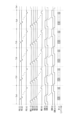
- 4 is a timing chart for explaining an outline of an operation in a normal drive mode of the display device according to the first embodiment.
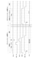
- 5 is a timing chart for explaining an outline of an operation in a pause drive mode of the display device according to the first embodiment.
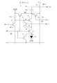
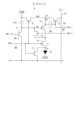
- FIG. 2 is a circuit diagram showing a configuration of a pixel circuit in the first embodiment.
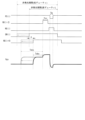
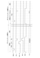
- 4 is a timing chart for explaining an operation of the pixel circuit in the first embodiment in a pause drive mode. 4 is a timing chart for explaining the effect of the first embodiment.
- FIG. 11 is a circuit diagram showing a configuration of a pixel circuit in a display device according to a second embodiment.
- FIG. 13 is a timing chart for explaining an operation in a pause drive mode of the pixel circuit in the second embodiment.
- FIG. 11 is a circuit diagram showing a first configuration example of a pixel circuit in a display device according to a third embodiment.
- 13 is a timing chart for explaining an operation of the pixel circuit in the pause drive mode in the third embodiment.
- FIG. 13 is a circuit diagram showing a second configuration example of the pixel circuit in the display device according to the third embodiment.
- 13A to 13D are circuit diagrams for explaining several configuration examples of a pixel circuit according to the fourth embodiment.
- FIG. 13 is a circuit diagram showing a configuration of a pixel circuit in a display device according to a fifth embodiment. 13 is a timing chart for explaining an operation of the pixel circuit in the fifth embodiment in a pause drive mode.
- the gate terminal corresponds to the control terminal
- one of the drain terminal and the source terminal corresponds to the first conduction terminal
- the other corresponds to the second conduction terminal.
- the transistor is, for example, a thin film transistor, but the present invention is not limited to this.
- connection means “electrical connection” unless otherwise specified, and includes not only direct connection but also indirect connection via other elements within the scope of the present invention.
- First embodiment ⁇ 1.1 Overall configuration> 1 is a block diagram showing the overall configuration of a display device 10 according to a first embodiment.
- the display device 10 is an organic EL display device that performs internal compensation, and each pixel circuit in the display device 10 has a function of compensating for variations and fluctuations in the threshold voltage of the internal driving transistor.
- the display device 10 also has two operation modes, a normal drive mode and a pause drive mode.
- the display device 10 in the normal drive mode, the display device 10 operates so that refresh frame periods Trf in which image data (data voltages in each pixel circuit) of the display unit are continuously repeated, and in the pause drive mode, the display device 10 operates so that a drive period TD consisting of only the refresh frame period Trf and a pause period TP consisting of a plurality of non-refresh frame periods Tnrf in which rewriting of image data of the display unit is stopped appear alternately.
- the display device 10 includes a display unit 11, a display control circuit 20, a data side drive circuit 30, a scanning side drive circuit 40, and a power supply circuit 50.
- the data side drive circuit 30 functions as a data signal line drive circuit.
- the scanning side drive circuit 40 functions as a scanning signal line drive circuit and a light emission control circuit.
- these two scanning side circuits are realized as a single scanning side drive circuit 40, but these two circuits may be appropriately separated, or these two circuits may be separated and arranged on one side and the other side of the display unit 11.
- at least a part of the data side drive circuit and the scanning side drive circuit may be formed integrally with the display unit 11.
- the power supply circuit 50 generates a high-level power supply voltage ELVDD, a low-level power supply voltage ELVSS, and an initialization voltage Vini, which are described below, to be supplied to the display unit 11, and a power supply voltage (not shown) to be supplied to the display control circuit 20, the data side drive circuit 30, and the scanning side drive circuit 40.
- the display unit 11 is provided with m (m is an integer of 2 or more) data signal lines D1, D2, ..., Dm, n first scanning signal lines PS1, PS2, ..., PSn that intersect with the data signal lines, and n+2 (n is an integer of 2 or more) second scanning signal lines NS-1, NS0, NS1, ..., NSn.
- the display unit 11 is also provided with n+1 light emission control lines EM1 to EMn+1 that intersect with the data signal lines D1, D2, ..., Dm, and of these, the n light emission control lines EM1 to EMn are respectively arranged along the n first scanning signal lines PS1, PS2, ..., PSn.
- the display unit 11 is also provided with m x n pixel circuits 15 arranged in a matrix along the m data signal lines D1 to Dm and the n first scanning signal lines PS1 to PSn.
- Each pixel circuit 15 corresponds to one of the m data signal lines D1 to Dm and to one of the n first scanning signal lines PS1 to PSn (hereinafter, when distinguishing between the pixel circuits 15, the pixel circuit corresponding to the i-th first scanning signal line PSi and the j-th data signal line Dj is also referred to as the "pixel circuit in the i-th row and j-th column" and is indicated by the symbol "Pix(i, j)").
- Each pixel circuit 15 also corresponds to one of the n second scanning signal lines NS1 to NSn and to one of the n emission control lines EM1 to EMn.
- the data side drive circuit 30 that drives the data signal lines D1, D2, ..., Dm, and the scan side drive circuit 40 that drives the first scanning signal lines PS1, PS2, ..., PSn, the second scanning signal lines NS-1, NS0, NS1, ..., NSn, and the light emission control lines EM1 to EMn constitute a drive circuit that drives the m x n pixel circuits 15 in the display unit 11.
- the display unit 11 is also provided with a power supply line (not shown) common to each pixel circuit 15. That is, a first power supply line (hereinafter referred to as a "high-level power supply line” and indicated with the symbol “ELVDD” like the high-level power supply voltage) for supplying a high-level power supply voltage ELVDD for driving an organic EL element described below, and a second power supply line (hereinafter referred to as a “low-level power supply line” and indicated with the symbol “ELVSS” like the low-level power supply voltage) for supplying a low-level power supply voltage ELVSS for driving an organic EL element are provided.
- a first power supply line hereinafter referred to as a "high-level power supply line” and indicated with the symbol “ELVDD” like the high-level power supply voltage
- ELVDD high-level power supply voltage
- ELVSS low-level power supply line
- the display unit 11 is also provided with an initialization voltage line (not shown) (indicated with the symbol “Vini” like the initialization voltage) for supplying an initialization voltage Vini used in a reset operation (also called an "initialization operation") for initializing each pixel circuit 15.
- the high-level power supply voltage ELVDD, the low-level power supply voltage ELVSS, and the initialization voltage Vini are supplied from the power supply circuit 50.
- the display control circuit 20 receives an input signal Sin from outside the display device 10, which includes image information representing the image to be displayed and timing control information for image display, generates a data-side control signal Scd and a scanning-side control signal Scs based on this input signal Sin, and outputs the data-side control signal Scd to the data-side drive circuit 30 and the scanning-side control signal Scs to the scan-side drive circuit 40.
- the data side drive circuit 30 drives the data signal lines D1 to Dm based on the data side control signal Scd from the display control circuit 20. That is, during the refresh frame period Trf, the data side drive circuit 30 generates m data signals D(1) to D(m) representing the image to be displayed based on the data side control signal Scd and applies them to the data signal lines D1 to Dm, respectively.
- the scanning side drive circuit 40 functions as a scanning signal line drive circuit that drives the n first scanning signal lines PS1 to PSn and the n+2 second scanning signal lines NS-1 to NSn, and as a light emission control circuit that drives the n+1 light emission control lines EM1 to EMn+1, based on the scanning side control signal Scs from the display control circuit 20. That is, the scanning side drive circuit 40, as a scanning signal line drive circuit, selects the n first scanning signal lines PS1 to PSn in sequence for a predetermined period corresponding to one horizontal period, and selects the n+2 second scanning signal lines NS-1 to NSn in sequence for a predetermined period corresponding to one horizontal period, based on the scanning side control signal Scs, during the refresh frame period Trf.
- the scanning side drive circuit 40 also drives the light emission control lines EM1 to EMn so that they are selectively deactivated in conjunction with the above-mentioned driving of the first and second scanning signal lines PS1 to PSn, NS-1 to NSn, during the refresh frame period Trf.
- the period during which the i-th light emission control line EMi is in an active state is the light emission period of the i-th row pixel circuits Pix(i,1) to Pix(i,m), and the period during which the i-th light emission control line EMi is in an inactive state is the non-light emission period of the i-th row pixel circuits Pix(i,1) to Pix(i,m). As shown in FIG.
- P type P-channel type
- N type N-channel type
- Figure 2 is a timing chart for explaining the general operation of the display device 10 in the normal drive mode.
- the scanning side drive circuit 40 In the normal drive mode, the scanning side drive circuit 40 generates the first scanning signals PS(1), PS(2), ..., PS(n) and the second scanning signals NS(-1), NS(0), NS(1), ..., NS(n) as shown in Figure 2 based on the scanning side control signal Scs provided by the display control circuit 20, applies the first scanning signals PS(1) to PS(n) to the first scanning signal lines PS1 to PSn, respectively, and applies the second scanning signals NS(-1) to NS(n) to the second scanning signal lines NS-1 to NSn, respectively.
- the scanning side drive circuit 40 generates the light emission control signals EM(1) to EM(n+1) as shown in Figure 2 based on the scanning side control signal Scs, and applies them to the light emission control lines EM1 to EMn+1, respectively.
- the data side drive circuit 30 generates data signals D(1) to D(m) that change in conjunction with the first scanning signals PS(1) to PS(n) as shown in FIG. 2 based on the data side control signal Scd from the display control circuit 20, and applies them to the data signal lines D1 to Dm, respectively.
- the first scanning signal lines PS1 to PSn, the second scanning signal lines NS-1 to NSn, the light emission control lines EM1 to EMn+1, and the data signal lines D1 to Dm in the display unit 11 are driven, and during the non-light emission period, initialization and writing of data voltages are performed for each pixel circuit Pix(i,j), and during the light emission period, each pixel circuit Pix(i,j) emits light with a luminance according to the written data voltage.
- the first scanning signal lines PS1 to PSn, the second scanning signal lines NS-1 to NSn, the emission control lines EM1 to EMn+1, and the data signal lines D1 to Dm are driven as described above by the various signals shown in FIG. 2, and a refresh frame period Trf is repeated in which the first scanning signal lines PS1 to PSn and the second scanning signal lines NS-1 to NSn are selected in sequence during one frame period to write image data to the pixel circuits Pix(1,1) to Pix(n,m) of the display unit 11.
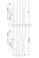
- FIG. 3 is a timing chart for explaining the general operation of the display device 10 in the pause drive mode.
- a drive period TD consisting of the above-mentioned refresh frame period (hereinafter also referred to as "RF frame period”) Trf and a pause period TP consisting of a plurality of non-refresh frame periods (hereinafter also referred to as "NRF frame periods”) Tnrf are alternately repeated.
- RF frame period the refresh frame period
- NRF frame periods non-refresh frame periods
- the driving of the first scanning signal lines PS1 to PSn and the second scanning signal lines NS-1 to NSn by the scanning side drive circuit 40 and the driving of the data signal lines D1 to Dm by the data side drive circuit 30 are stopped, and the display of the image data written in the previous drive period TD (RF frame period Trf) continues.
- the pause drive mode is effective in reducing the power consumption of the display device 10 when displaying a still image.
- the drive period TD is composed of only one RF frame period Trf, but it may be composed of two or more RF frame periods Trf.
- the external input signal Sin includes an operation mode signal Sm indicating whether the display unit 11 is to be driven in the normal drive mode or the pause drive mode.
- This operation mode signal Sm is provided to the scanning side drive circuit 40 as a part of the scanning side control signal Scs, and is provided to the data side drive circuit 30 as a part of the data side control signal Scd.
- the scanning side drive circuit 40 drives the first scanning signal lines PS1 to PSn and the second scanning signal lines NS-1 to NSn according to the operation mode indicated by this operation mode signal Sm, and drives the emission control lines EM1 to EMn+1 in the same form (same period and same duty) regardless of whether it is the normal drive mode or the pause drive mode.
- the data side drive circuit 30 drives the data signal lines D1 to Dn according to the operation mode indicated by this operation mode signal Sm. Note that since the problem of this application is not related to the normal drive mode, the operation of the display device 10 or its pixel circuits will be described below mainly in the pause drive mode (the same applies to other embodiments described later).
- a data write operation is performed for each pixel circuit Pix(i,j) when the corresponding first and second scanning signal lines PSi, NSi are in a selected state, and an initialization operation is performed when the second scanning signal line NSi-2, which is two lines before the second scanning signal line NSi, is in a selected state.
- P-type transistors are used as the first and second light emission control transistors T5, T6, so that each light emission control line EMi is activated when a low level (L level) voltage is applied, and is deactivated when a high level (H level) voltage is applied.
- Configuration of pixel circuit> 4 is a circuit diagram showing the configuration of a pixel circuit 15 in this embodiment, more specifically, the configuration of a pixel circuit 15 corresponding to the i-th first scanning signal line PSi and the j-th data signal line Dj, that is, the pixel circuit Pix(i,j) in the i-th row and j-th column (1 ⁇ i ⁇ n, 1 ⁇ j ⁇ m).
- This pixel circuit 15 includes one organic EL element OL as a display element, seven transistors T1 to T7 (hereinafter, these are referred to as the "first initialization transistor T1", the “threshold compensation transistor T2", the “write control transistor T3", the “drive transistor T4", the “first emission control transistor T5", the “second emission control transistor T6”, and the “second initialization transistor T7”), and one storage capacitor Cst.
- this pixel circuit 15 also includes a bias application circuit 151 including a bias application capacitor Cob.
- the transistors T1, T2, and T7 are N-type transistors, and the transistors T3 to T6 are P-type transistors.
- the N-type transistors T1, T2, and T7 are thin-film transistors (hereinafter referred to as "oxide TFTs") whose channel layers are formed of an oxide semiconductor, and more specifically, oxide TFTs (hereinafter referred to as "IGZO-TFTs”) that use indium gallium zinc oxide (InGaZnO) as the oxide semiconductor.
- Oxide TFTs have a small off-leak current, making them suitable as switching elements in pixel circuits and the like.
- the P-type transistors T3 to T6 are thin-film transistors (hereinafter referred to as "LTPS-TFTs") whose channel layers are formed of low-temperature polysilicon.
- Low-temperature polysilicon has high mobility, so when the LTPS-TFTs are used as driving transistors, the driving ability for the organic EL element in the pixel circuit is improved, and when used as switching elements, the on-resistance is reduced.
- the transistors that can be used in the pixel circuit 15 are not limited to IGZO-TFTs or LTPS-TFTs.
- the transistors T1 to T3 and T5 to T7 other than the drive transistor T4 operate as switching elements.
- a pixel circuit Pix(i, j) includes a corresponding first scanning signal line PSi (hereinafter, in the description focusing on the pixel circuit, it is also referred to as a "corresponding first scanning signal line”), a corresponding second scanning signal line NSi (hereinafter, in the description focusing on the pixel circuit, it is also referred to as a “corresponding second scanning signal line”), a corresponding light emission control line EMi (hereinafter, in the description focusing on the pixel circuit, it is also referred to as a "corresponding light emission control line”), and a corresponding data signal line (hereinafter, in the description focusing on the pixel circuit, it is also referred to as a "corresponding second scanning signal line”)
- the corresponding second scanning signal line NSi also referred to as the "corresponding data signal line” in the description that focuses on the pixel circuit
- Dj the second scanning signal line
- X which specifies the subsequent emission control line EMi+X connected to the pixel circuit Pix(i,j), is an integer equal to or greater than 0, and is selected such that the emission control signal EM(i+X) of the subsequent emission control line EMi+X changes from L level to H level during the RF frame period Trf between when the corresponding emission control line EMi for the pixel circuit Pix(i,j) changes to the inactive state and when data writing with threshold compensation is started (see FIG. 5 described later).
- X is preferably an integer equal to or greater than 1.
- "until data writing with threshold compensation is started” corresponds to "until the write control transistor T3 changes to the ON state due to the change of the corresponding first scanning signal PS(i) to the L level,” but it is preferable to select X such that the emission control signal EM(i+X) of the subsequent emission control line EMi+X changes from L level to H level before the threshold compensation transistor T2 changes to the ON state due to the change of the corresponding second scanning signal NS(i) to the H level.
- the signal PS(i) of the corresponding first scanning signal line PSi, the signal NS(i) of the corresponding second scanning signal line NSi, the signal NS(i) of the preceding second scanning signal line NSi-2, the signal EM(i) of the corresponding light-emission control line EMi, the signal EM(i+X) of the following light-emission control line EMi+X, and the signal D(j) of the corresponding data signal line Dj will be referred to as the corresponding first scanning signal PS(i), the corresponding second scanning signal NS(i), the preceding second scanning signal NS(i-2), the corresponding light-emission control signal EM(i), the following light-emission control signal EM(i+X), and the corresponding data signal D(j), respectively.
- the source terminal of the driving transistor T4 is connected to the corresponding data signal line Dj via the write control transistor T3, and is connected to the high-level power supply line ELVDD via the first emission control transistor T5.
- the drain terminal of the driving transistor T4 is connected to the anode as the first terminal of the organic EL element OL via the second emission control transistor T6, and the cathode as the second terminal of the organic EL element OL is connected to the low-level power supply line ELVSS.
- the gate terminal of the driving transistor T4 is connected to the drain terminal of the driving transistor T4 via the threshold compensation transistor T2, and is connected to the high-level power supply line ELVDD via the holding capacitor Cst, and is connected to the initialization voltage line Vini via the first initialization transistor T1.
- the anode of the organic EL element OL is also connected to the initialization voltage line Vini via the second initialization transistor T7 as a display element initialization transistor.
- the bias application circuit 151 has a first terminal connected to the subsequent light emission control line EMi+X and a second terminal connected to the source terminal of the drive transistor T4, and includes the bias application capacitor Cob described above, and the first terminal is connected to the second terminal via the bias application capacitor Cob.
- Fig. 5 is a timing chart for explaining the operation of the pixel circuit Pix(i,j) in the non-emission period included in the RF frame period Trf and the NRF frame period Tnrf. Note that Fig. 5 shows a plurality of dotted lines extending in the vertical direction, and the interval between these dotted lines corresponds to one horizontal period.
- the period when the emission control signal EM(i) is at H level is the non-emission period
- the period when the emission control signal EM(i) is at L level is the emission period (these points are the same in Figs. 6, 8, 10, and 14 showing the timing charts described later).
- the first and second light-emitting control transistors T5 and T6 are in the OFF state, so the organic EL element OL is in the OFF state, and the second initialization transistor T7 is in the ON state, so that the anode of the organic EL element OL is initialized.
- the preceding second scanning signal NS(i-2) first goes to H level for a predetermined period equivalent to approximately one horizontal period, and during this predetermined period (hereinafter referred to as the "initialization period Tini"), the first initialization transistor T1 is in the on state, so that the voltage of the holding capacitor Cst and the gate terminal of the drive transistor T4 (hereinafter referred to as the "gate voltage”) is initialized to the initialization voltage Vini.
- the corresponding second scanning signal NS(i) becomes H level for a predetermined period corresponding to approximately one horizontal period, and within this predetermined period, the corresponding first scanning signal PS(i) becomes L level for a predetermined period corresponding to approximately one horizontal period.
- the horizontal period during which the corresponding second scanning signal NS(i) becomes H level and the corresponding first scanning signal PS(i) becomes L level is called the "compensation/write period Tw" or simply the "write period Tw".
- the threshold compensation transistor T2 is turned on, so that the drive transistor T4 is in a diode-connected state, and the write control transistor T3 is turned on, so that the voltage Vdata of the corresponding data signal D(j) is written to the holding capacitor Cst via the drive transistor T4 in a diode-connected state.
- the gate terminal of the drive transistor T4 is held at the data voltage (Vdata-
- Vth is the threshold voltage of the drive transistor T4.
- a subsequent light emission control signal EM(i+X) is applied to the first terminal of the bias application circuit 151.
- the write control transistor T3, the first and second light emission control transistors T5 and T6, and the threshold compensation transistor T2 are all in the off state, and the node NdS including the source terminal of the drive transistor T4 is in a floating state, so that the voltage of the source terminal (hereinafter also referred to as the "source voltage") Vs changes in the same direction as the change of the subsequent light emission control signal EM(i+X) from L level to H level. That is, the source voltage Vs of the driving transistor T4 rises in response to the change in the subsequent light emission control signal EM(i+X) from L level to H level.
- the increase in the source voltage Vs can be made approximately equal to the voltage difference between the L level and H level of the subsequent light emission control signal EM(i+X) by setting the capacitance of the bias application capacitor Cob to be sufficiently larger than the parasitic capacitance added to the node NdS.
- the above operation applies a relatively large voltage stress (Vgs) to the drive transistor T4 from the point when the subsequent light emission control signal EM(i+X) changes from L level to H level (see the upward arrow in FIG. 5) to the start of the initialization period Tini (the point when the preceding second scanning signal NS(i-2) changes to H level).
- the period during which a relatively large voltage stress (Vgs) is applied to the drive transistor T4 in this manner is the on-bias application period Tobs.
- the end point of this on-bias application period Tobs does not depend on the light emission duty, and the length of the period increases as the light emission duty decreases. This point will be explained below with reference to FIG. 6.
- FIG. 6 is a timing chart for explaining the relationship between the on-bias application period Tobs and the light emission duty during the RF frame period Trf.
- the light emission duty is adjusted by changing the rising timing of the light emission control signal EM(i) (this is similar to other embodiments described below). For this reason, when the light emission duty is low (when the brightness is set to low), the rising timing of the light emission control signal EM(i) is early, and the rising timing of the subsequent light emission control signal EM(i+X) is also early accordingly, so that the period Tobs during which a relatively large on-bias voltage Vobs (voltage stress Vgs) is applied to the drive transistor T4 becomes longer.
- Vobs voltage stress Vgs
- the lower the light emission duty during the RF frame period Trf the longer the on-bias application period Tobs becomes. This is also true for the NRF frame period Tnrf.
- the subsequent light emission control signal EM(i+X) changes from L level to H level between the time when the corresponding light emission control line EMi changes to an inactive state and the time when data writing begins, so that the drive transistor T4 is in a state in which a relatively large voltage stress (Vgs) is applied.
- Vgs relatively large voltage stress
- the data voltage Vdata is written during the write period Tw after the on-bias application period Tobs, and the gate terminal of the drive transistor T4 is thereby held at the data voltage (Vdata-
- the corresponding light emission control signal EM(i) changes to the L level, thereby starting the light emission period.
- the first and second light emission control transistors T5 and T6 are in the ON state, and the other transistors T1, T2, T3, and T7, except for the drive transistor T4, are in the OFF state.
- a current I1 according to the data voltage Vdata written to the holding capacitor Cst flows through the organic EL element OL, and the organic EL element OL emits light with a brightness according to the current I1.
- the operation of the pixel circuit Pix(i,j) during the non-light-emitting period in the NRF frame period Tnrf will be described.
- the driving of the first scanning signal lines PS1 to PSn and the second scanning signal lines NS-1 to NSn is stopped, so that, as shown in FIG. 5, the corresponding first scanning signal PS(i) is maintained at the H level, and the preceding second scanning signal NS(i-2) and the corresponding second scanning signal NS(i) are maintained at the L level.
- the first and second light-emitting control transistors T5 and T6 are in the OFF state during the non-light-emitting period, so that the organic EL element OL is in the OFF state, and the second initialization transistor T7 is in the ON state, so that the anode of the organic EL element OL is initialized.
- the subsequent light emission control signal EM(i+X) changes from L level to H level.
- the subsequent light emission control signal EM(i+X) changes to H level one horizontal period after the corresponding light emission control signal EM(i) changes to H level.
- This subsequent light emission control signal EM(i+X) is provided to the first terminal of the bias application circuit 151, and as shown in FIG. 4, this first terminal is connected to the source terminal of the drive transistor T4 via the bias application capacitor Cob.
- the write control transistor T3, the first and second light emission control transistors T5 and T6, and the threshold compensation transistor T2 are all in the off state, and the node NdS including the source terminal of the drive transistor T4 is in a floating state. Therefore, the voltage (source voltage) Vs of the source terminal of the driving transistor T4 changes in the same direction as the change of the subsequent light emission control signal EM(i+X) from L level to H level. That is, the source voltage Vs of the driving transistor T4 rises in response to the change of the subsequent light emission control signal EM(i+X) from L level to H level.
- the source voltage Vs whose level has risen in this way is maintained until the time when the corresponding light emission control signal EM(i) changes to L level (the end time of the non-light emission period). Therefore, in the NRF frame period Tnrf, the period from when the subsequent light emission control signal EM(i+X) changes to H level to when the corresponding light emission control signal EM(i) changes to L level is called the "on-bias application period Tobs". In addition, in the NRF frame period Tnrf, the first initialization transistor T1, the threshold compensation transistor T2, and the write control transistor T3 are maintained in the off state (see FIG. 4 and FIG. 5). Additionally, the data signals D(1) to D(m) applied to the data signal lines D1 to Dm are all maintained in a high impedance state.
- the corresponding light emission control signal EM(i) changes to the L level and the light emission period begins.
- the pixel circuit Pix(i,j) operates in the same manner as during the light emission period in the RF frame period Trf.
- the source voltage Vs whose level has increased due to the change of the subsequent light-emitting control signal EM(i+X) to H level, is applied as an on-bias voltage to the source terminal of the drive transistor T4 during the on-bias application period Tobs.
- Vgs voltage stress
- the period during which the voltage stress (Vgs) on the driving transistor T4 becomes a small value (Vth) when data is written is about one horizontal period long and is relatively very short, so the decrease in the stress voltage (Vgs) during this period does not cause a problem in the above-mentioned flicker suppression.
- the flicker suppression effect can be obtained in pause driving without complicating the configuration and driving of the pixel circuit.
- bias control lines (hereinafter referred to as "bias control lines") PSB1 to PSBn are arranged along n first scanning signal lines PS1 to PSn.
- Each pixel circuit 15 corresponds to one of the n bias control lines PB1 to PBn.
- the scanning side driving circuit 40 in this embodiment also functions as a bias control circuit that generates bias control signals PSB(1) to PSB(n) described later in the pause driving mode and applies them to the bias control lines PB1 to PBn, respectively, to drive the bias control lines PB1 to PBn (see FIG. 8).
- the normal driving mode the driving of the bias control lines PSB1 to PSBn is stopped, and all of the bias control lines PSB1 to PSBn are maintained in an inactive state.
- FIG. 7 is a circuit diagram showing the configuration of pixel circuit Pix(i,j) in row i and column j (1 ⁇ i ⁇ n, 1 ⁇ j ⁇ m), which is pixel circuit 15 in this embodiment.
- This pixel circuit 15 has the same configuration as pixel circuit 15 in the first embodiment (FIG. 4), except for the configuration of bias application circuit 151.
- the pixel circuit Pix(i,j) in the i-th row and j-th column which is the pixel circuit 15 in this embodiment, is connected to the corresponding first scanning signal line PSi, the bias control line PSBi corresponding to the pixel circuit Pix(i,j) (hereinafter, also referred to as the "corresponding bias control line” in the description focusing on the pixel circuit), the corresponding second scanning signal line NSi, the preceding second scanning signal line NSi-2, the corresponding emission control line EMi, the corresponding data signal line Dj, the initialization voltage line Vini, the high-level power supply line ELVDD, and the low-level power supply line ELVSS.
- the bias application circuit 151 provided in this pixel circuit 15 has a first terminal connected to the corresponding first scanning signal line PSi and receiving the voltage of the corresponding first scanning signal PS(i) in the inactive state as an on-bias voltage, and a second terminal connected to the source terminal of the drive transistor T4, and includes a P-type bias application transistor T8 having a source terminal and a drain terminal connected to the first and second terminals, respectively.
- the bias application transistor T8 has a gate terminal connected to the corresponding bias control line PSBi and operates as a switching element.
- FIG. 8 is a timing chart for explaining the operation of the pixel circuit Pix(i,j) during the non-emission periods included in the RF frame period Trf and the NRF frame period Tnrf.
- the first scanning signal PS(i), the second scanning signal NS(i), NS(i-2), the light emission control signal EM(i), and the data signal D(j) for driving the pixel circuit Pix(i,j) in this embodiment change in the same way as the first scanning signal PS(i), the second scanning signal NS(i), NS(i-2), the light emission control signal EM(i), and the data signal D(j) for driving the pixel circuit Pix(i,j) in the first embodiment.
- the transistors T1 to T3, T5 to T7 as switching elements included in the pixel circuit 15 in this embodiment operate in the same way as the transistors T1 to T3, T5 to T7 as switching elements included in the pixel circuit 15 in the first embodiment, thereby performing the same initialization operation and data writing operation.
- the corresponding light emission control signal EM(i) changes to the L level
- the light emission period begins, and as in the first embodiment, the organic EL element OL emits light with a luminance according to the data voltage Vdata written to the storage capacitor by the data write operation.
- the corresponding bias control signal PSB(i) is at L level for a predetermined period from when the corresponding emission control signal EM(i) changes from L level to H level to start the non-emission period until the preceding second scanning signal NS(i-2) changes from L level to H level to start the initialization period Tini.
- the voltage of the corresponding first scanning signal line PSi is applied as an on-bias voltage to the source terminal of the drive transistor T4 via the bias application transistor T8.
- the corresponding bias control signal PSB(i) changes to H level to turn off the bias application transistor T8, but the voltage of the source terminal of the drive transistor T4 (source voltage Vs) is maintained until the corresponding second scanning signal NS(i) changes to H level to turn on the threshold compensation transistor T2. Furthermore, until the preceding second scanning signal NS(i-2) changes to H level and the first initialization transistor T1 is turned on, the voltage of the gate terminal of the drive transistor T4 (gate voltage Vg) is maintained at a voltage corresponding to the holding voltage of the holding capacitor Cst.
- the operation of the pixel circuit Pix(i,j) during the non-light-emitting period in the NRF frame period Tnrf will be described.
- the corresponding first scanning signal PS(i) is at H level
- the preceding second scanning signal NS(i-2) and the corresponding second scanning signal NS(i) are at L level, as in the case of the RF frame period Trf described above.
- the first and second light-emitting control transistors T5 and T6 are in the OFF state, so the organic EL element OL is in the OFF state, and the anode of the organic EL element OL is initialized because the second initialization transistor T7 is in the ON state.
- the corresponding bias control signal PSB(i) changes in the same way as during the RF frame period Trf, but during the NRF frame period Tnrf, the first scanning signal PS(i) is maintained at H level, and the preceding second scanning signal NS(i-2) and the corresponding second scanning signal NS(i) are maintained at L level.
- the bias application transistor T8 While the corresponding bias control signal PSB(i) is at L level, the bias application transistor T8 is turned on, and during this L level period, the voltage of the corresponding first scanning signal line PSi is applied as an on-bias voltage to the source terminal of the driving transistor T4 via the bias application transistor T8.
- the corresponding bias control signal PSB(i) changes to H level and the bias application transistor T8 is turned off, but the source terminal of the driving transistor T4 is in a floating state until the corresponding light emission control signal EM(i) becomes L level and the first and second light emission control transistors T5 and T6 become ON, and the voltage Vg of the gate terminal of the driving transistor T4 becomes a voltage corresponding to the voltage Vdata written to the holding capacitor Cst.
- this period in the NRF frame period Tnrf is also called the "on-bias application period Tobs.”
- the corresponding light emission control signal EM(i) changes to the L level and the light emission period begins.
- the operation of the pixel circuit Pix(i,j) during the light emission period in the NRF frame period Tnrf is the same as in the first embodiment.
- a corresponding bias control line PSBi is connected to the gate terminal of the bias application transistor T8 constituting the bias application circuit 151, and the bias application transistor T8 is turned on and off by the corresponding bias control signal PSB(i).
- X is appropriately set for the first scanning signal PS(i-X) (X is an integer of 2 or more) preceding the corresponding first scanning signal PS(i)
- the preceding first scanning signal PS(i-X) can be used as the corresponding bias control signal PSB(i).
- the first scanning signal PS(i) is generated so that the first scanning signal PS(i) is at the L level for a predetermined period even during the non-refresh period in the NRF frame period, as shown by the dotted line in FIG. 8.
- the above-mentioned effect can be obtained with a simpler configuration without providing a circuit for generating the bias control signals PSB(1) to PSB(n) or the bias control lines PSB1 to PSBn.
- the corresponding first scanning signal line PSi is connected to a first terminal of the bias application circuit 151, and the H-level voltage of the corresponding first scanning signal PS(i) is applied to the bias application circuit 151 as an on-bias voltage.
- another signal line may be connected to the first terminal as long as it has a voltage that can be used as an on-bias voltage.
- the corresponding emission control line EMi may be connected to the first terminal of the bias application circuit 151.
- First configuration example> 9 is a circuit diagram showing a first configuration example of the pixel circuit 15 in this embodiment, more specifically, a circuit diagram showing the configuration of the pixel circuit Pix(i,j) in the i-th row and j-th column (1 ⁇ i ⁇ n, 1 ⁇ j ⁇ m).
- This pixel circuit 15 has the same configuration as the pixel circuit 15 in the first embodiment (FIG. 4) except for the configuration of the bias application circuit 151.
- the pixel circuit Pix(i,j) in the i-th row and j-th column which is the pixel circuit 15 in this embodiment, is connected to the corresponding first scanning signal line PSi, the corresponding second scanning signal line NSi, the preceding second scanning signal line NSi-2, the corresponding light emission control line EMi, the corresponding data signal line Dj, the initialization voltage line Vini, the high-level power supply line ELVDD, and the low-level power supply line ELVSS, and is further connected to the preceding second scanning signal line NSi-X.
- X is a positive integer, and is selected so that the period during the RF frame period Trf during which the second scanning signal NS(i-X) in the preceding second scanning signal line NSi-X is at the H level is included between the time when the corresponding light emission control line EMi for the pixel circuit Pix(i,j) changes to the inactive state and the time when data writing with threshold compensation is started (see FIG. 10 described later).
- X is preferably an integer of 2 or more.
- "until data writing with threshold compensation is started” corresponds to "until the write control transistor T3 is turned on due to the corresponding first scanning signal PS(i) changing to the L level", but it is preferable to select X so that the second scanning signal NS(i-X) in the preceding second scanning signal line NSi-X changes from H level to L level before the threshold compensation transistor T2 is turned on due to the corresponding second scanning signal NS(i) changing to the H level.
- bias control second scanning signal line NSi-X the preceding second scanning signal line NSi-X specified by such X
- the signal of the bias control second scanning signal line NSi-X is referred to as the “bias control second scanning signal NS(i-X)" (the same applies to other embodiments described later).
- the bias application circuit 151 provided in the pixel circuit 15 has a first terminal connected to the bias control second scanning signal line NSi-X and receives the voltage of the bias control second scanning signal NS(i-X) as an on-bias voltage Vobs, and a second terminal connected to the source terminal of the drive transistor T4, and includes a P-type bias application transistor T8 having a source terminal and a drain terminal connected to the first and second terminals, respectively.
- This bias application transistor T8 has its gate terminal connected to its drain terminal, forming a diode connection.
- FIG. 10 is a timing chart for explaining the operation of the pixel circuit Pix(i,j) during the non-emission periods included in the RF frame period Trf and the NRF frame period Tnrf.
- the first scanning signal PS(i), the second scanning signal NS(i), NS(i-2), the light emission control signal EM(i), and the data signal D(j) for driving the pixel circuit Pix(i,j) in this embodiment change in the same way as the first scanning signal PS(i), the second scanning signal NS(i), NS(i-2), the light emission control signal EM(i), and the data signal D(j) for driving the pixel circuit Pix(i,j) in the first embodiment.
- the transistors T1 to T3, T5 to T7 as switching elements included in the pixel circuit Pix(i,j) in this embodiment operate in the same way as the transistors T1 to T3, T5 to T7 as switching elements included in the pixel circuit 15 in the first embodiment, and similar initialization operations and data writing operations are performed.
- the bias application circuit 151 receives the second scanning signal for bias control NS(i-X) at its first terminal.
- This first terminal is connected to the source terminal of the drive transistor T4 via a P-type bias application transistor T8 in a diode-connected configuration as shown in FIG. 9. Therefore, when the second scanning signal for bias control NS(i-X) is at H level, the H-level voltage is applied to the source terminal of the drive transistor T4 via the bias application transistor T8.
- the value of X that specifies the second scanning signal for bias control NS(i-X) is selected as described above, so that the period during which the second scanning signal for bias control NS(i-X) is at H level is usually only at H level for a predetermined period from when the corresponding light emission control signal EM(i) changes to H level to when the initialization period Tini starts when the preceding second scanning signal NS(i-2) changes to H level, as shown in Figure 10.
- the second scanning signal for bias control NS(i-X) changes to L level to turn off the bias application transistor T8, but until the initialization period Tini starts when the preceding second scanning signal NS(i-2) changes to H level, a relatively large voltage stress (Vgs) based on the H level voltage of the second scanning signal for bias control NS(i-X) is applied to the drive transistor T4.
- Vgs voltage stress
- the period from when the second scanning signal for bias control NS(i-X) changes to the H level in the RF frame period Trf until the initialization period Tini starts is called the "on-bias application period Tobs.”
- the operation of the pixel circuit Pix(i,j) after the initialization period Tini in the RF frame period Trf is the same as in the first embodiment.
- the corresponding first scanning signal line PSi is driven, and the corresponding data signal line Dj is driven so that the on-bias voltage Vobs is applied from the corresponding data signal line Dj to the source terminal of the drive transistor T4 via the write control transistor T3 during the selection period of the corresponding first scanning signal line PSi (the period during which the corresponding first scanning signal PS(i) is at the L level) from the corresponding first scanning signal PS(i) to the corresponding light emission control signal EM(i) changing to the L level during the non-light emission period, a relatively large voltage stress (Vgs) based on the on-bias voltage Vobs applied from the corresponding data signal line Dj during the selection period of the first scanning signal PS(i) is applied to the drive transistor T4.
- this period is the "on-bias application period Tobs".
- the corresponding light emission control signal EM(i) changes to the L level and the light emission period begins.
- the operation of the pixel circuit Pix(i,j) during the light emission period in the NRF frame period Tnrf is the same as in the first embodiment.
- Second configuration example> 11 is a circuit diagram showing a second configuration of the pixel circuit 15 in this embodiment, more specifically, a circuit diagram showing the configuration of the pixel circuit Pix(i,j) in the i-th row and j-th column (1 ⁇ i ⁇ n, 1 ⁇ j ⁇ m).
- This pixel circuit 15 differs from the pixel circuit 15 according to the first configuration example (FIG. 9) in that the bias application transistor T8 in the bias application circuit 151 is an N-type transistor, but the other configurations are the same as those of the first configuration example.
- the drain terminal and source terminal of the bias application transistor T8 are connected to the first and second terminals of the bias application circuit 151 in this configuration example, respectively, and the bias application transistor T8 has its gate terminal connected to its drain terminal to form a diode connection.
- the pixel circuit Pix(i,j) according to this configuration example also operates in the same manner as the pixel circuit Pix(i,j) according to the first configuration example above, with the first scanning signal PS(i), second scanning signals NS(i), NS(i-2), NS(i-X), light emission control signal EM(i), and data signal D(j) that change as shown in FIG. 10. Therefore, even when the pixel circuit Pix(i,j) according to this configuration example is used in this embodiment, the same effect as when the pixel circuit Pix(i,j) according to the first configuration example above is used can be obtained.
- FIG. 12 are circuit diagrams for explaining first to fourth configuration examples of the pixel circuit in this embodiment, respectively, and show the configuration of the portion of the pixel circuit 15 shown in FIG. 11 surrounded by a dashed line. All of the pixel circuits 15 according to the first to fourth configuration examples in this embodiment have the same configuration as the pixel circuit 15 according to the second configuration example in the third embodiment (FIG. 11) except for the bias application circuit 151.
- the bias application circuit 151 provided in any of the pixel circuits 15 according to the first to fourth configuration examples includes an N-type bias application transistor T8 having a first terminal that receives an on-bias voltage Vobs and a second terminal connected to the source terminal of the drive transistor T4, and having a drain terminal and a source terminal connected to the first and second terminals, respectively.
- this bias application transistor T8 has a gate terminal connected to the second scanning signal line NSi-X for bias control, and operates as a switching element.
- the positive integer X that specifies this second scanning signal line NSi-X for bias control is selected in the same manner as in the third embodiment.
- a voltage line (hereinafter referred to as a "gate high level voltage line") for supplying a high level voltage VGH of the first scanning signal PS(i) or the second scanning signal NS(i) is connected to the first terminal of the bias application circuit 151, and the voltage VGH is applied as the on-bias voltage Vobs.
- a high level power supply line ELVDD is connected to the first terminal of the bias application circuit 151, and the high level power supply voltage ELVDD is applied as the on-bias voltage Vobs.
- a corresponding first scanning signal line PSi is connected to the first terminal of the bias application circuit 151, and the high level voltage of the corresponding first scanning signal PS(i) is applied as the on-bias voltage Vobs.
- the corresponding light emission control line EMi is connected to the first terminal of the bias application circuit 151, and the H-level voltage of the light emission control signal EM(i) is applied as the on-bias voltage Vobs.
- the signal line or voltage line connected to the first terminal of the bias application circuit 151 differs depending on the first to fourth configurations.
- the pixel circuits Pix(i,j) according to the first to fourth configuration examples in this embodiment all operate in the same manner as the pixel circuit Pix(i,j) in the third embodiment, using the first scanning signal PS(i), second scanning signals NS(i), NS(i-2), NS(i-X), light emission control signal EM(i), and data signal D(j) that change as shown in FIG. 10. Therefore, according to this embodiment, regardless of which of the first to fourth configuration examples is adopted for the pixel circuit Pix(i,j), the same effect as the third embodiment can be obtained.
- an N-type bias application transistor T8 is used (see FIG. 12), but instead, a P-type bias application transistor T8 may be used, and the gate terminal of the bias application transistor T8 may be connected to the first scanning signal line PSi-X preceding the corresponding first scanning signal line PSi.
- FIG. 13 is a circuit diagram showing the configuration of pixel circuit Pix(i,j) in row i and column j (1 ⁇ i ⁇ n, 1 ⁇ j ⁇ m), which is pixel circuit 15 in this embodiment.
- This pixel circuit 15 has the same configuration as pixel circuit 15 in the first embodiment (FIG. 4), except for the connection form of bias application capacitor Cob that constitutes bias application circuit 151.
- the bias application circuit 151 provided in the pixel circuit Pix(i,j) also has a first terminal connected to its second terminal via a bias application capacitor Cob.
- the bias application circuit 151 has a first terminal connected to the corresponding first scanning signal line PSi and a second terminal connected to the source terminal (node NdS) of the drive transistor T4. Therefore, the gate terminal of the write control transistor T3 to which the corresponding first scanning signal line PSi is connected is connected to the node NdS including the drain terminal of the write control transistor T3 via the bias application capacitor Cob.
- the parasitic capacitance between the gate and drain of the write control transistor T3 of the pixel circuit Pix(i,j) may be used as the bias application capacitor Cob.
- FIG. 14 is a timing chart for explaining the operation of the pixel circuit Pix(i,j) during the non-emission periods included in the RF frame period Trf and the NRF frame period Tnrf.
- the scanning side drive circuit 40 in this embodiment drives the first scanning signal lines PS1 to PSn in the RF frame period Trf so that, for the pixel circuit Pix(i,j) corresponding to each first scanning signal line PSi, the corresponding first scanning signal line PSi is not only in the selected state during the writing period Tw, but is also in the selected state for a predetermined period from the start of the non-emission period to the start of the writing period Tw.
- the scanning side drive circuit 40 in this embodiment drives the first scanning signal lines PS1 to PSn in the RF frame period Trf so that, for the pixel circuit Pix(i,j) corresponding to each first scanning signal line PSi, the corresponding first scanning signal line PSi is not only in the selected state during the writing period Tw, but is also in the selected state for a predetermined period from the start of the non-emission period to the start of the writing period Tw.
- the first scanning signal PS(i), second scanning signals NS(i), NS(i-2), light emission control signal EM(i), and data signal D(j) for driving the pixel circuit Pix(i,j) in this embodiment change in the same way as the first scanning signal PS(i), second scanning signals NS(i), NS(i-2), light emission control signal EM(i), and data signal D(j) for driving the pixel circuit Pix(i,j) in the first embodiment.
- the transistors T1 to T3, T5 to T7 as switching elements included in the pixel circuit Pix(i,j) in this embodiment operate in the same manner as the transistors T1 to T3, T5 to T7 as switching elements included in the pixel circuit Pix(i,j) in the first embodiment, thereby performing the same initialization operation and data writing operation.
- the bias application circuit 151 receives the corresponding first scanning signal PS(i) at its first terminal.
- the corresponding first scanning signal PS(i) becomes L level for a predetermined period during the RF frame period Trf from the start of the non-emission period due to the change of the corresponding emission control signal EM(i) to H level to the start of the writing period Tw due to the change of the corresponding first scanning signal PS(i) to L level.
- the corresponding first scanning signal PS(i) becomes L level for a predetermined period before the start of the initialization period Tini. In this way, when the corresponding first scanning signal PS(i) changes from L level to H level after the start of the non-emission period and before the start of the initialization period Tini (see the upward arrow in FIG.
- the first emission control transistor T5 is in the OFF state, and the write control transistor T3 changes from the ON state to the OFF state. Therefore, the voltage (source voltage) Vs of the source terminal of the drive transistor T4 changes in the same direction as the change of the corresponding first scanning signal PS(i) from L level to H level. In other words, the source voltage Vs of the drive transistor T4 rises in response to the change of the corresponding first scanning signal PS(i) from L level to H level.
- the first scanning signal lines PS1 to PSn are driven so that the corresponding first scanning signal PS(i) is at L level for a predetermined period during the non-light-emitting period even during the NRF frame period Tnrf.
- the first scanning signal lines PS1 to PSn may be driven so that the corresponding first scanning signal PS(i) is at L level only once during the non-light-emitting period, but may also be driven so that it is at L level twice, including the pulse shown by the dotted line in FIG. 14.
- each data signal line Dj is in a high impedance state during the NRF frame period Tnrf.
- the corresponding first scanning signal PS(i) for each pixel circuit Pix(i,j) becomes L level for a predetermined period during the non-light emitting period (see FIG. 14), and a relatively large voltage stress (Vgs) is applied to the drive transistor T4 from the time when the corresponding first scanning signal PS(i) first changes from L level to H level during the non-light emitting period to the time when the corresponding light emitting control signal EM(i) changes from H level to L level and the light emitting period begins.
- Vgs voltage stress
- the difference in the stress state of the drive transistor T4 between the RF frame period Trf and the NRF frame period Tnrf is reduced regardless of the light emission duty, and the occurrence of flicker is sufficiently suppressed in the pause drive mode.
- there is no need for a separate voltage line or control line for applying an on-bias voltage to the drive transistor T4 so as in the first embodiment, such a flicker suppression effect can be obtained in the pause drive mode without complicating the configuration or drive of the pixel circuit.
- the pixel circuit 15 includes both P-type and N-type transistors, and typically, for the P-type transistors, LTPS-TFTs with high mobility are used, and for the N-type transistors, oxide TFTs such as IGZO-TFTs with good off-leakage characteristics are used.
- oxide TFTs such as IGZO-TFTs with good off-leakage characteristics are used.
- the channel type of the transistor to be used may be appropriately changed between P-type and N-type to be configured to operate in the same way.
- a configuration using N-type LTPS-TFTs instead of P-type LTPS-TFTs may be adopted.
- pixel circuits 15 configured as shown in FIG. 4 etc. are used, but the configuration of the pixel circuit is not limited to this, and any pixel circuit may be used as long as it is an internal compensation type pixel circuit including a threshold compensation transistor, and is configured to hold the data voltage written to the holding capacitor while allowing the application of an on-bias voltage to reduce threshold shifts due to the hysteresis characteristics of the drive transistor.
- the light emission control lines EM1 to EMn are usually driven so that the light emission duty is the same in both the RF frame period Trf and the NRF frame period Tnrf, but the device may be configured so that different light emission duties can be set in the RF frame period Trf and the NRF frame period Tnrf.
- the first embodiment is configured to adjust the light emission duty by changing the rising timing of the light emission control signal EM(i), i.e., the start timing of the non-light emission period, as shown in FIG. 6.
- the light emission duty may be adjusted by changing the falling timing of the light emission control signal EM(i), i.e., the end timing of the non-light emission period, without changing the rising timing of the light emission control signal EM(i). This is also true for other embodiments.
- an on-bias application period Tobs is provided in the non-light emission period within the RF frame period from the start of the non-light emission period to the start of the writing period Tw, the former configuration is more advantageous than the latter configuration in that it can sufficiently suppress the occurrence of flicker in the pause drive mode regardless of the light emission duty.
- an on-bias application period may also be provided from the end of the writing period Tw to the end of the non-light emission period. In this way, whether the former or latter configuration is used to adjust the light emission duty, it is possible to sufficiently suppress the occurrence of flicker in the pause drive mode regardless of the light emission duty.
- Display elements that can be used here include, for example, organic EL elements, i.e., organic light-emitting diodes (Organic Light Emitting Diodes (OLEDs)), inorganic light-emitting diodes, quantum dot light-emitting diodes (Quantum dot Light Emitting Diodes (QLEDs)), etc.
- organic EL elements i.e., organic light-emitting diodes (Organic Light Emitting Diodes (OLEDs)), inorganic light-emitting diodes, quantum dot light-emitting diodes (Quantum dot Light Emitting Diodes (QLEDs)), etc.
- OLEDs Organic Light Emitting Diodes
- QLEDs Quantum dot Light Emitting Diodes
- ELVDD High-level power supply line (first power supply line), high-level power supply voltage
- ELVSS Low-level power supply line (second power supply line)
- OL Organic EL element (display element)
- Cst ... holding capacitor Cob ... bias application capacitor T1 ... first initialization transistor T2 ... threshold compensation transistor T3 ... data write control transistor T4 ... drive transistor T5 ... first light emission control transistor T6 ... second light emission control transistor T7 ... second initialization transistor T8 ... bias application transistor TD ... drive period TP ... idle period Trf ... refresh frame period (RF frame period) Tnrf...non-refresh frame period (NRF frame period)
- Vobs On-bias voltage
Landscapes
- Engineering & Computer Science (AREA)
- Physics & Mathematics (AREA)
- Computer Hardware Design (AREA)
- General Physics & Mathematics (AREA)
- Theoretical Computer Science (AREA)
- Control Of Indicators Other Than Cathode Ray Tubes (AREA)
Abstract
本願は、低周波駆動を行う電流駆動型の表示装置であって、画素回路の構成や駆動の複雑化を抑えつつ駆動トランジスタへのオンバイアス電圧の印加によりフリッカの発生を十分に抑制できる表示装置を開示する。内部補償方式の表示装置が休止駆動モードで動作する場合に、リフレッシュフレーム期間と非リフレッシュフレーム期間のいずれの非発光期間においても、画素回路内の駆動トランジスタにオンバイアス電圧を印加するためのオンバイアス印加期間Tobsが設けられる。リフレッシュフレーム期間内の非発光期間では、非発光期間が開始されてからデータ電圧の画素回路への書込開始までの間にオンバイアス電圧の印加が行われるように、既存の信号線および電圧線を介して当該画素回路が駆動される。これにより、リフレッシュフレーム期間と非リフレッシュフレーム期間との間での駆動トランジスタのストレス状態の差異が低減される。
Description
本発明は表示装置に関し、より詳しくは、有機EL(Electro Luminescence)素子等の電流で駆動される表示素子を備えた電流駆動型の表示装置、および、その駆動方法に関する。
近年、有機EL素子(有機発光ダイオード(Organic Light Emitting Diode: OLED)とも呼ばれる)を用いた有機EL表示装置が実用化されている。有機EL素子は、それに流れる電流に応じた輝度で発光する自発光型表示素子である。有機EL表示装置の画素回路には、有機EL素子に加えて、それに流れる電流を制御する駆動トランジスタ等が含まれている。この駆動トランジスタの特性にばらつきや変動が発生することから、有機EL表示装置において高画質表示を行うためには、この特性のばらつきや変動を補償する必要がある。そこで、有機EL表示装置の画素回路では、その内部で駆動トランジスタにおける閾値電圧のばらつきや変動を補償するように構成されたものがある(以下、このような閾値電圧のばらつきや変動の補償を「閾値補償」といい、このように画素回路内で閾値補償を行う方式を「内部補償方式」という)。
一方、消費電力を低減するために低周波駆動を行えるように構成された表示装置が知られている。このような表示装置では、例えば静止画を表示するときに、リフレッシュ動作を行う隣接するフレーム期間の間にリフレッシュ動作を行わないフレーム期間を挿入することによりリフレッシュレートを大きく低下させた低周波駆動を行うことで、消費電力を大幅に低減することができる。
有機EL表示装置において低周波駆動を行う場合、各画素回路における有機EL素子は、リフレッシュ動作を行うフレーム期間であるリフレッシュフレーム期間では、フレーム期間毎に設けられる非発光期間に発光制御トランジスタにより消灯状態とされるが、リフレッシュ動作を行わないフレーム期間である非リフレッシュフレーム期間では、駆動回路の動作が停止し、その前のリフレッシュフレーム期間において当該画素回路に書き込まれたデータ電圧に応じた輝度で発光を続ける。一般に、静止画表示を行う場合、リフレッシュ動作を行わずに表示を継続する期間(これは連続する複数の非リフレッシュフレーム期間から構成され、以下「休止期間」という)は、リフレッシュ動作を行う期間(1つのリフレッシュフレーム期間または連続する複数のリフレッシュフレーム期間から構成され、以下「駆動期間」という)に比べ格段に長く、表示動作中に、そのような駆動期間と休止期間とが交互に現れる。このため、低周波駆動により静止画を表示すると、駆動期間における有機EL素子の消灯がフリッカとして視認されることになる。
これに対し特許文献1には、低周波駆動を行う場合に視認されるフリッカを解消すべく、駆動期間(データリフレッシュ期間T_refrech)での有機EL素子(発光ダイオード304)の消灯による輝度低下に加えて、休止期間(拡張ブランキング期間T_blank)においても適切な頻度で輝度低下が生じるように構成された画素回路とその駆動方法が記載されている。
しかし、有機EL表示装置が低周波駆動を行う場合に休止期間においても適切な頻度で輝度低下が生じるように構成されていても(以下、このような構成を「周期的消灯構成」という)、画素回路における駆動トランジスタとしての薄膜トランジスタはヒステリシス特性を有することから、低周波駆動において依然としてフリッカが視認される。
これに対し上記の特許文献1には、駆動期間(データリフレッシュ期間T_refrech)のみならず休止期間(拡張ブランキング期間T_blank)においても、駆動トランジスタに意図的にバイアスストレス電圧(以下「オンバイアス電圧」または単に「バイアス電圧」という)を印加して、ヒステリシス特性による(有機EL素子の輝度への)影響をバランスさせることが記載されている。また、特許文献2においても、有機発光ダイオードディスプレイの低周波駆動において、駆動トランジスタのヒステリシス特性を軽減するために駆動トランジスタにオンバイアス電圧を印加する構成が記載されている。
しかし、特許文献1や特許文献2に記載の表示装置では、駆動トランジスタにオンバイアス電圧を印加するために画素回路の構成や駆動の複雑化を招く。これは、表示の高精細化を妨げ回路規模を増大させる要因となる。
そこで、低周波駆動を行う有機EL表示装置のような電流駆動型の表示装置において、画素回路の構成や駆動の複雑化を抑えつつ駆動トランジスタへのオンバイアス電圧の印加によりフリッカの発生を十分に抑制することが望まれている。
本発明の幾つかの実施形態に係る表示装置は、
複数の画素回路を含む表示部と、
前記複数の画素回路を駆動する駆動回路と、
前記複数の画素回路に複数のデータ信号の電圧をデータ電圧として書き込む1つまたは複数のリフレッシュフレーム期間からなる駆動期間と前記複数の画素回路へのデータ電圧の書き込みを停止する1つまたは複数の非リフレッシュフレーム期間からなる休止期間とが交互に現れるように前記駆動回路を制御する表示制御回路と
を備え、
前記複数の画素回路のそれぞれは、
電流によって駆動される表示素子と、
制御端子と第1導通端子と第2導通端子とを有し、前記表示素子と直列に設けられた駆動トランジスタと、
前記駆動トランジスタの前記制御端子の電圧を保持するために一端が前記駆動トランジスタの前記制御端子に接続された保持キャパシタと、
前記保持キャパシタに書き込むべきデータ電圧を受け取る第1導通端子と前記駆動トランジスタの前記第1導通端子に接続された第2導通端子とを有するスイッチング素子としての書込制御トランジスタと、
前記駆動トランジスタの前記第2導通端子と前記制御端子との間に設けられ、オン状態のときに前記駆動トランジスタをダイオード接続状態とするスイッチング素子としての閾値補償トランジスタと、
前記表示素子および前記駆動トランジスタに対し直列に設けられたスイッチング素子としての少なくとも1つの発光制御トランジスタと、
前記駆動トランジスタのヒステリシス特性による閾値電圧のシフトを低減するためのバイアス電圧を前記駆動トランジスタの前記第1導通端子に印加するバイアス印加回路と
を含み、
前記複数の画素回路のそれぞれにおいて、前記バイアス印加回路は、当該画素回路または他の画素回路におけるトランジスタのうち前記バイアス印加回路に含まれないトランジスタの制御端子に与えられる信号の1つまたは前記複数の画素回路の電源電圧の1つを受け取る第1端子と、前記駆動トランジスタの前記第1導通端子に接続された第2端子とを有し、前記第1端子において受け取る前記信号または前記電圧に基づき前記バイアス電圧を前記駆動トランジスタの前記第1導通端子に与えるように構成されている。
複数の画素回路を含む表示部と、
前記複数の画素回路を駆動する駆動回路と、
前記複数の画素回路に複数のデータ信号の電圧をデータ電圧として書き込む1つまたは複数のリフレッシュフレーム期間からなる駆動期間と前記複数の画素回路へのデータ電圧の書き込みを停止する1つまたは複数の非リフレッシュフレーム期間からなる休止期間とが交互に現れるように前記駆動回路を制御する表示制御回路と
を備え、
前記複数の画素回路のそれぞれは、
電流によって駆動される表示素子と、
制御端子と第1導通端子と第2導通端子とを有し、前記表示素子と直列に設けられた駆動トランジスタと、
前記駆動トランジスタの前記制御端子の電圧を保持するために一端が前記駆動トランジスタの前記制御端子に接続された保持キャパシタと、
前記保持キャパシタに書き込むべきデータ電圧を受け取る第1導通端子と前記駆動トランジスタの前記第1導通端子に接続された第2導通端子とを有するスイッチング素子としての書込制御トランジスタと、
前記駆動トランジスタの前記第2導通端子と前記制御端子との間に設けられ、オン状態のときに前記駆動トランジスタをダイオード接続状態とするスイッチング素子としての閾値補償トランジスタと、
前記表示素子および前記駆動トランジスタに対し直列に設けられたスイッチング素子としての少なくとも1つの発光制御トランジスタと、
前記駆動トランジスタのヒステリシス特性による閾値電圧のシフトを低減するためのバイアス電圧を前記駆動トランジスタの前記第1導通端子に印加するバイアス印加回路と
を含み、
前記複数の画素回路のそれぞれにおいて、前記バイアス印加回路は、当該画素回路または他の画素回路におけるトランジスタのうち前記バイアス印加回路に含まれないトランジスタの制御端子に与えられる信号の1つまたは前記複数の画素回路の電源電圧の1つを受け取る第1端子と、前記駆動トランジスタの前記第1導通端子に接続された第2端子とを有し、前記第1端子において受け取る前記信号または前記電圧に基づき前記バイアス電圧を前記駆動トランジスタの前記第1導通端子に与えるように構成されている。
本発明の他の幾つかの実施形態に係る駆動方法は、電流によって駆動される表示素子を用いた表示装置の駆動方法であって、
前記表示装置は、複数の画素回路を含む表示部を備え、
前記複数の画素回路のそれぞれは、
電流によって駆動される表示素子と、
制御端子と第1導通端子と第2導通端子とを有し、前記表示素子と直列に設けられた駆動トランジスタと、
前記駆動トランジスタの前記制御端子の電圧を保持するために一端が前記駆動トランジスタの前記制御端子に接続された保持キャパシタと、
前記保持キャパシタに書き込むべきデータ電圧を受け取る第1導通端子と前記駆動トランジスタの前記第1導通端子に接続された第2導通端子とを有するスイッチング素子としての書込制御トランジスタと、
前記駆動トランジスタの前記第2導通端子と前記制御端子との間に設けられ、オン状態のときに前記駆動トランジスタをダイオード接続状態とするスイッチング素子としての閾値補償トランジスタと、
前記表示素子および前記駆動トランジスタに対し直列に設けられたスイッチング素子としての少なくとも1つの発光制御トランジスタと、
前記駆動トランジスタのヒステリシス特性による閾値電圧のシフトを低減するためのバイアス電圧を前記駆動トランジスタの前記第1導通端子に印加するバイアス印加回路と
を含み、
前記複数の画素回路のそれぞれにおいて、前記バイアス印加回路は、当該画素回路または他の画素回路におけるトランジスタのうち前記バイアス印加回路に含まれないトランジスタの制御端子に与えられる信号の1つまたは前記複数の画素回路の電源電圧の1つを受け取る第1端子と、前記駆動トランジスタの前記第1導通端子に接続された第2端子とを有し、
前記駆動方法は、前記複数の画素回路に複数のデータ信号の電圧をデータ電圧として書き込む1つまたは複数のリフレッシュフレーム期間からなる駆動期間と前記複数の画素回路へのデータ電圧の書き込みを停止する1つまたは複数の非リフレッシュフレーム期間からなる休止期間とが交互に現れるように、前記複数の画素回路を駆動する休止駆動ステップを備え、
前記休止駆動ステップは、前記リフレッシュフレーム期間および前記非リフレッシュフレーム期間のいずれにおいても、前記複数の画素回路のそれぞれにおいて前記発光制御トランジスタがオフ状態である期間内に、前記バイアス印加回路が前記第1端子において受け取る前記信号または前記電圧に基づき前記バイアス電圧を前記駆動トランジスタの前記第1導通端子に印加するように、前記複数の画素回路を駆動するバイアス印加ステップを含む。
前記表示装置は、複数の画素回路を含む表示部を備え、
前記複数の画素回路のそれぞれは、
電流によって駆動される表示素子と、
制御端子と第1導通端子と第2導通端子とを有し、前記表示素子と直列に設けられた駆動トランジスタと、
前記駆動トランジスタの前記制御端子の電圧を保持するために一端が前記駆動トランジスタの前記制御端子に接続された保持キャパシタと、
前記保持キャパシタに書き込むべきデータ電圧を受け取る第1導通端子と前記駆動トランジスタの前記第1導通端子に接続された第2導通端子とを有するスイッチング素子としての書込制御トランジスタと、
前記駆動トランジスタの前記第2導通端子と前記制御端子との間に設けられ、オン状態のときに前記駆動トランジスタをダイオード接続状態とするスイッチング素子としての閾値補償トランジスタと、
前記表示素子および前記駆動トランジスタに対し直列に設けられたスイッチング素子としての少なくとも1つの発光制御トランジスタと、
前記駆動トランジスタのヒステリシス特性による閾値電圧のシフトを低減するためのバイアス電圧を前記駆動トランジスタの前記第1導通端子に印加するバイアス印加回路と
を含み、
前記複数の画素回路のそれぞれにおいて、前記バイアス印加回路は、当該画素回路または他の画素回路におけるトランジスタのうち前記バイアス印加回路に含まれないトランジスタの制御端子に与えられる信号の1つまたは前記複数の画素回路の電源電圧の1つを受け取る第1端子と、前記駆動トランジスタの前記第1導通端子に接続された第2端子とを有し、
前記駆動方法は、前記複数の画素回路に複数のデータ信号の電圧をデータ電圧として書き込む1つまたは複数のリフレッシュフレーム期間からなる駆動期間と前記複数の画素回路へのデータ電圧の書き込みを停止する1つまたは複数の非リフレッシュフレーム期間からなる休止期間とが交互に現れるように、前記複数の画素回路を駆動する休止駆動ステップを備え、
前記休止駆動ステップは、前記リフレッシュフレーム期間および前記非リフレッシュフレーム期間のいずれにおいても、前記複数の画素回路のそれぞれにおいて前記発光制御トランジスタがオフ状態である期間内に、前記バイアス印加回路が前記第1端子において受け取る前記信号または前記電圧に基づき前記バイアス電圧を前記駆動トランジスタの前記第1導通端子に印加するように、前記複数の画素回路を駆動するバイアス印加ステップを含む。
本発明の上記幾つかの実施形態によれば、電流によって駆動される表示素子、駆動トランジスタ、書込制御トランジスタ、閾値補償トランジスタ、発光制御トランジスタ、および、保持キャパシタを含む画素回路を備えた内部補償方式の表示装置において、各画素回路は、駆動トランジスタのヒステリシス特性による閾値電圧のシフトを低減するためのバイアス電圧を駆動トランジスタの第1導通端子に印加するためのバイアス印加回路を更に含んでいる。表示部における上記複数の画素回路のそれぞれにおいて、バイアス印加回路は、当該画素回路または他の画素回路におけるトランジスタのうちバイアス印加回路に含まれないトランジスタの制御端子に与えられる信号の1つまたは上記複数の画素回路の電源電圧の1つを受け取る第1端子と、駆動トランジスタの第1導通端子に接続された第2端子とを有している。このような表示装置において、リフレッシュフレーム期間からなる駆動期間と非リフレッシュフレーム期間からなる休止期間とが交互に現れる休止駆動が行われる場合に、バイアス印加回路が第1端子において受け取る上記信号または上記電圧に基づき上記バイアス電圧が駆動トランジスタの第1導通端子に与えられる。これにより、休止駆動を行う場合であっても、リフレッシュフレーム期間と非リフレッシュフレーム期間の間での駆動トランジスタのストレス状態の差異を低減し、画素回路の構成や駆動の複雑化を招くことなくフリッカを抑制することができる。
以下、添付図面を参照しつつ実施形態について説明する。なお、以下で言及する各トランジスタにおいて、ゲート端子は制御端子に相当し、ドレイン端子およびソース端子の一方は第1導通端子に相当し、他方は第2導通端子に相当する。また、以下の各実施形態におけるトランジスタは例えば薄膜トランジスタであるが、本発明はこれに限定されない。さらにまた、本明細書における「接続」とは、特に断らない限り「電気的接続」を意味し、本発明の要旨を逸脱しない範囲において、直接的な接続を意味する場合のみならず、他の素子を介した間接的な接続を意味する場合も含むものとする。
<1.第1の実施形態>
<1.1 全体構成>
図1は、第1の実施形態に係る表示装置10の全体構成を示すブロック図である。この表示装置10は、内部補償を行う有機EL表示装置であり、この表示装置10における各画素回路は、その内部の駆動トランジスタの閾値電圧のばらつきや変動を補償する機能を有している。また、この表示装置10は、通常駆動モードと休止駆動モードとの2つの動作モードを有している。すなわち表示装置10は、通常駆動モードでは、表示部の画像データ(各画素回路内のデータ電圧)を書き換えるリフレッシュフレーム期間Trfが連続するように動作し、休止駆動モードでは、リフレッシュフレーム期間Trfのみからなる駆動期間TDと表示部の画像データの書き換えを停止する複数の非リフレッシュフレーム期間Tnrfからなる休止期間TPとが交互に現れるように動作する。
<1.1 全体構成>
図1は、第1の実施形態に係る表示装置10の全体構成を示すブロック図である。この表示装置10は、内部補償を行う有機EL表示装置であり、この表示装置10における各画素回路は、その内部の駆動トランジスタの閾値電圧のばらつきや変動を補償する機能を有している。また、この表示装置10は、通常駆動モードと休止駆動モードとの2つの動作モードを有している。すなわち表示装置10は、通常駆動モードでは、表示部の画像データ(各画素回路内のデータ電圧)を書き換えるリフレッシュフレーム期間Trfが連続するように動作し、休止駆動モードでは、リフレッシュフレーム期間Trfのみからなる駆動期間TDと表示部の画像データの書き換えを停止する複数の非リフレッシュフレーム期間Tnrfからなる休止期間TPとが交互に現れるように動作する。
図1に示すように、この表示装置10は、表示部11、表示制御回路20、データ側駆動回路30、走査側駆動回路40、および、電源回路50を備えている。データ側駆動回路30は、データ信号線駆動回路として機能する。走査側駆動回路40は、走査信号線駆動回路および発光制御回路として機能する。図1に示す構成ではこれら走査側の2つの回路が1つの走査側駆動回路40として実現されているが、これら2つの回路が適宜分離された構成であってもよく、また、これら2つの回路が表示部11の一方側と他方側に分離されて配置される構成であってもよい。また、データ側駆動回路および走査側駆動回路の少なくとも一部が表示部11と一体的に形成されていてもよい。これらの点は、後述の他の実施形態や変形例においても同様である。電源回路50は、表示部11に供給すべき後述のハイレベル電源電圧ELVDD、ローレベル電源電圧ELVSS、および初期化電圧Viniと、表示制御回路20、データ側駆動回路30、および走査側駆動回路40に供給すべき電源電圧(不図示)とを生成する。
表示部11には、m本(mは2以上の整数)のデータ信号線D1,D2,…,Dmと、これらに交差するn本の第1走査信号線PS1,PS2,…,PSnおよびn+2本(nは2以上の整数)の第2走査信号線NS-1,NS0,NS1,…,NSnとが配設されている。また、表示部11には、データ信号線D1,D2,…,Dmに交差するn+1本の発光制御線EM1~EMn+1が設けられており、これらのうちn本の発光制御線EM1~EMnは、n本の第1走査信号線PS1,PS2,…,PSnにそれぞれ沿って配設されている。また表示部11には、m本のデータ信号線D1~Dmおよびn本の第1走査信号線PS1~PSnに沿ってマトリクス状に配置されたm×n個の画素回路15が設けられている。各画素回路15は、m本のデータ信号線D1~Dmのいずれか1つに対応するとともにn本の第1走査信号線PS1~PSnのいずれか1つに対応する(以下、各画素回路15を区別する場合には、i番目の第1走査信号線PSiおよびj番目のデータ信号線Djに対応する画素回路を「i行j列目の画素回路」ともいい、符号“Pix(i,j)”で示す)。また各画素回路15は、n本の第2走査信号線NS1~NSnのいずれか1つに対応するとともに、n本の発光制御線EM1~EMnのいずれか1つに対応する。なお、上記のデータ信号線D1,D2,…,Dmを駆動するデータ側駆動回路30と、上記の第1走査信号線PS1,PS2,…,PSn、第2走査信号線NS-1,NS0,NS1,…,NSn、および、発光制御線EM1~EMnを駆動する走査側駆動回路40とは、表示部11におけるm×n個の画素回路15を駆動する駆動回路を構成する。
また表示部11には、各画素回路15に共通の図示しない電源線が配設されている。すなわち、後述の有機EL素子を駆動するためのハイレベル電源電圧ELVDDを供給するための第1電源線(以下「ハイレベル電源線」といい、ハイレベル電源電圧と同じく符号“ELVDD”で示す)、および、有機EL素子を駆動するためのローレベル電源電圧ELVSSを供給するための第2電源線(以下「ローレベル電源線」といい、ローレベル電源電圧と同じく符号“ELVSS”で示す)が配設されている。さらに表示部11には、各画素回路15の初期化のためのリセット動作(「初期化動作」ともいう)に使用する初期化電圧Viniを供給するための図示しない初期化電圧線(初期化電圧と同じく符号“Vini”で示す)も配設されている。ハイレベル電源電圧ELVDD、ローレベル電源電圧ELVSS、および初期化電圧Viniは、電源回路50から供給される。
表示制御回路20は、表示すべき画像を表す画像情報および画像表示のためのタイミング制御情報を含む入力信号Sinを表示装置10の外部から受け取り、この入力信号Sinに基づきデータ側制御信号Scdおよび走査側制御信号Scsを生成し、データ側制御信号Scdをデータ側駆動回路30に、走査側制御信号Scsを走査側駆動回路40にそれぞれ出力する。
データ側駆動回路30は、表示制御回路20からのデータ側制御信号Scdに基づきデータ信号線D1~Dmを駆動する。すなわちデータ側駆動回路30は、リフレッシュフレーム期間Trfにおいて、データ側制御信号Scdに基づき、表示すべき画像を表すm個のデータ信号D(1)~D(m)を生成してデータ信号線D1~Dmにそれぞれ印加する。
走査側駆動回路40は、表示制御回路20からの走査側制御信号Scsに基づき、n本の第1走査信号線PS1~PSnおよびn+2本の第2走査信号線NS-1~NSnを駆動する走査信号線駆動回路、および、n+1本の発光制御線EM1~EMn+1を駆動する発光制御回路として機能する。すなわち走査側駆動回路40は、リフレッシュフレーム期間Trfにおいて、走査信号線駆動回路として、走査側制御信号Scsに基づき、n本の第1走査信号線PS1~PSnを1水平期間に対応する所定期間ずつ順次に選択するとともに、n+2本の第2走査信号線NS-1~NSnを1水平期間に対応する所定期間ずつ順次に選択する。また走査側駆動回路40は、リフレッシュフレーム期間Trfにおいて、発光制御線EM1~EMnを、それらが第1および第2走査信号線PS1~PSn,NS-1~NSnの上記駆動に連動して選択的に非活性化されるように駆動する。i番目の発光制御線EMiが活性化状態である期間は、i行目の画素回路Pix(i,1)~Pix(i,m)の発光期間であり、i番目の発光制御線EMiが非活性化状態である期間は、i行目の画素回路Pix(i,1)~Pix(i,m)の非発光期間である。なお、後述の図4に示すように本実施形態では、第1走査信号線PSi1は画素回路15内のPチャネル型(以下「P型」ともいう)トランジスタのゲート端子に接続され(i1=1~n)、第2走査信号線NSi2は画素回路15内のNチャネル型(以下「N型」ともいう)トランジスタのゲート端子に接続される(i2=-1~n)。このため、選択した第1走査信号線PSi1にはアクティブな信号としてローレベル電圧が印加され、選択した第2走査信号線NSi2にはアクティブな信号としてハイレベル電圧が印加される。
<1.2 概略動作>
以下、図2および図3を参照して、通常駆動モードおよび休止駆動モードにおける表示装置10の概略動作を説明する。
以下、図2および図3を参照して、通常駆動モードおよび休止駆動モードにおける表示装置10の概略動作を説明する。
図2は、通常駆動モードにおける表示装置10の概略動作を説明するためのタイミングチャートである。通常駆動モードにおいて走査側駆動回路40は、表示制御回路20から与えられる走査側制御信号Scsに基づき、図2に示すような第1走査信号PS(1),PS(2),…,PS(n)および第2走査信号NS(-1),NS(0),NS(1),…,NS(n)を生成し、第1走査信号PS(1)~PS(n)を第1走査信号線PS1~PSnにそれぞれ印加し、第2走査信号NS(-1)~NS(n)を第2走査信号線NS-1~NSnにそれぞれ印加する。また、走査側駆動回路40は、上記走査側制御信号Scsに基づき、図2に示すような発光制御信号EM(1)~EM(n+1)を生成して発光制御線EM1~EMn+1にそれぞれ印加する。一方、データ側駆動回路30は、表示制御回路20からのデータ側制御信号Scdに基づき、図2に示すように第1走査信号PS(1)~PS(n)に連動して変化するデータ信号D(1)~D(m)を生成し、データ信号線D1~Dmにそれぞれ印加する。このようにして表示部11における第1走査信号線PS1~PSn、第2走査信号線NS-1~NSn、発光制御線EM1~EMn+1、および、データ信号線D1~Dmが駆動されることで、非発光期間において、各画素回路Pix(i,j)に対し初期化およびデータ電圧の書き込みが行われ、発光期間において、各画素回路Pix(i,j)は書き込まれたデータ電圧に応じた輝度で発光する。
通常駆動モードでは、図2に示した上記各種信号により第1走査信号線PS1~PSn、第2走査信号線NS-1~NSn、発光制御線EM1~EMn+1、および、データ信号線D1~Dmが上記のように駆動されることで、1フレーム期間において第1走査信号線PS1~PSnおよび第2走査信号線NS-1~NSnを順次選択して表示部11の画素回路Pix(1,1)~Pix(n,m)に画像データを書き込むリフレッシュフレーム期間Trfが繰り返される。
図3は、休止駆動モードにおける表示装置10の概略動作を説明するためのタイミングチャートである。休止駆動モードでは、図3に示すように、上記のリフレッシュフレーム期間(以下「RFフレーム期間」ともいう)Trfからなる駆動期間TDと、複数の非リフレッシュフレーム期間(以下「NRFフレーム期間」ともいう)Tnrfからなる休止期間TPとが交互に繰り返される。休止期間TP(NRFフレーム期間Tnrf)では、走査側駆動回路40による第1走査信号線PS1~PSnおよび第2走査信号線NS-1~NSnの駆動とデータ側駆動回路30によるデータ信号線D1~Dmの駆動とが停止し、直前の駆動期間TD(RFフレーム期間Trf)に書き込まれた画像データによる表示が継続する。このため休止駆動モードは、静止画を表示する場合において表示装置10の消費電力の削減に有効である。ただし、後述のように、休止期間TPにおいても第1走査信号線PS1~PSnが駆動される実施形態もある。なお、図3に示す例では駆動期間TDは1つのRFフレーム期間Trfのみから構成されるが、2つ以上のRFフレーム期間Trfから構成されていてもよい。
外部からの入力信号Sinには、上記のような通常駆動モードと休止駆動モードのうちいずれの動作モードで表示部11を駆動するかを示す動作モード信号Smが含まれている。この動作モード信号Smは、走査側制御信号Scsの一部として走査側駆動回路40に与えられるともに、データ側制御信号Scdの一部としてデータ側駆動回路30に与えられる。走査側駆動回路40は、この動作モード信号Smで示される動作モードに応じて第1走査信号線PS1~PSnおよび第2走査信号線NS-1~NSnを駆動し、発光制御線EM1~EMn+1を通常駆動モードか休止駆動モードかに拘わらず同様の形態(同一の周期および同一のデューティ)で駆動する。データ側駆動回路30は、この動作モード信号Smで示される動作モードに応じてデータ信号線D1~Dnを駆動する。なお、本願の課題は通常駆動モードとは関係しないので、以下において、表示装置10またはその画素回路の動作については休止駆動モードにおける動作を中心に説明する(後述の他の実施形態においても同様)。
本実施形態では、RFフレーム期間Trfにおいて、各画素回路Pix(i,j)に対し、それに対応する第1および第2走査信号線PSi,NSiが選択状態のときにデータ書込動作が行われ、その第2走査信号線NSiの2つ前の第2走査信号線NSi-2が選択状態のとき初期化動作が行われる。各画素回路Pix(i,j)がそのデータ書込動作および初期化動作が行われる期間において消灯状態となるように発光制御線EMiが駆動される(i=1~n)(図3参照)。後述のように、本実施形態における画素回路Pix(i,j)では、第1および第2発光制御トランジスタT5,T6としてP型トランジスタが使用されているので、各発光制御線EMiは、ローレベル(Lレベル)の電圧を与えられると活性化状態となり、ハイレベル(Hレベル)の電圧を与えられると非活性化状態となる。
<1.3 画素回路の構成>
図4は、本実施形態における画素回路15の構成を示す回路図であり、より詳しくは、i番目の第1走査信号線PSiおよびj番目のデータ信号線Djに対応する画素回路15すなわちi行j列目の画素回路Pix(i,j)の構成を示す回路図である(1≦i≦n、1≦j≦m)。この画素回路15は、表示素子としての1個の有機EL素子OLと、7個のトランジスタT1~T7(以下、これらを「第1初期化トランジスタT1」、「閾値補償トランジスタT2」、「書込制御トランジスタT3」、「駆動トランジスタT4」、「第1発光制御トランジスタT5」、「第2発光制御トランジスタT6」、「第2初期化トランジスタT7」という)と、1個の保持キャパシタCstとを含んでいる。また、この画素回路15は、これらの素子に加えて、バイアス印加キャパシタCobを含むバイアス印加回路151を含んでいる。
図4は、本実施形態における画素回路15の構成を示す回路図であり、より詳しくは、i番目の第1走査信号線PSiおよびj番目のデータ信号線Djに対応する画素回路15すなわちi行j列目の画素回路Pix(i,j)の構成を示す回路図である(1≦i≦n、1≦j≦m)。この画素回路15は、表示素子としての1個の有機EL素子OLと、7個のトランジスタT1~T7(以下、これらを「第1初期化トランジスタT1」、「閾値補償トランジスタT2」、「書込制御トランジスタT3」、「駆動トランジスタT4」、「第1発光制御トランジスタT5」、「第2発光制御トランジスタT6」、「第2初期化トランジスタT7」という)と、1個の保持キャパシタCstとを含んでいる。また、この画素回路15は、これらの素子に加えて、バイアス印加キャパシタCobを含むバイアス印加回路151を含んでいる。
この画素回路15において、トランジスタT1,T2,T7はN型トランジスタであり、トランジスタT3~T6はP型トランジスタである。本実施形態では、N型トランジスタT1,T2,T7は、チャネル層が酸化物半導体で形成された薄膜トランジスタ(以下「酸化物TFT」という)であり、より詳しくは酸化物半導体として酸化インジウムガリウム亜鉛(InGaZnO)を使用した酸化物TFT(以下、「IGZO-TFT」という)である。酸化物TFTは、オフリーク電流が小さいので、画素回路等におけるスイッチング素子として好適である。また、P型のトランジスタT3~T6は、チャネル層が低温ポリシリコンで形成された薄膜トランジスタ(以下「LTPS-TFT」という)である。低温ポリシリコンは移動度が高いので、LTPS-TFTを駆動トランジスタとして使用すると、画素回路において有機EL素子に対する駆動能力が向上し、スイッチング素子として使用するとオン抵抗が低くなる。ただし、画素回路15において使用可能なトランジスタは、このようなIGZO-TFTやLTPS-TFTには限定されない。なお、画素回路15において、駆動トランジスタT4以外のトランジスタT1~T3,T5~T7はスイッチング素子として動作する。
図1および図4に示すように、本実施形態における画素回路Pix(i,j)には、それに対応する第1走査信号線(以下、画素回路に注目した説明において「対応第1走査信号線」ともいう)PSiと、それに対応する第2走査信号線(以下、画素回路に注目した説明において「対応第2走査信号線」ともいう)NSiと、それに対応する発光制御線(以下、画素回路に注目した説明において「対応発光制御線」ともいう)EMiと、それに対応するデータ信号線(以下、画素回路に注目した説明において「対応データ信号線」ともいう)Djと、対応第2走査信号線NSiの2つ前の第2走査信号線(第2走査信号線NS-1~NSnの走査順における2つ前の走査信号線であり、以下、画素回路に注目した説明において単に「先行第2走査信号線」ともいう)NSi-2と、初期化電圧線Viniと、ハイレベル電源線ELVDDと、ローレベル電源線ELVSSとが接続されており、更に、対応発光制御線EMiに後続する発光制御線EMi+Xが接続されている。なお、画素回路Pix(i,j)に、先行第2走査信号線NSi-2に代えて直前の第2走査信号線NSi-1が接続される構成であってもよい。
本実施形態において画素回路Pix(i,j)に接続される上記後続の発光制御線EMi+Xを特定するXは、0以上の整数であって、RFフレーム期間Trfにおいて、画素回路Pix(i,j)につき対応発光制御線EMiが非活性化状態に変化してから閾値補償を伴うデータ書込が開始されるまでの間に上記後続の発光制御線EMi+Xの発光制御信号EM(i+X)がLレベルからHレベルへと変化するように選定されている(後述の図5参照)。ただし後述のように、Xは1以上の整数であることが好ましい。また、「閾値補償を伴うデータ書込が開始されるまで」とは「対応第1走査信号PS(i)のLレベルへの変化により書込制御トランジスタT3がオン状態に変化するまで」に相当するが、対応第2走査信号NS(i)のHレベルへの変化により閾値補償トランジスタT2がオン状態に変化する前に当該後続の発光制御線EMi+Xの発光制御信号EM(i+X)がLレベルからHレベルへと変化するようにXを選定するのが好ましい。
以下では、このような画素回路Pix(i,j)に関する説明において、対応第1走査信号線PSiの信号PS(i)、対応第2走査信号線NSiの信号NS(i)、先行第2走査信号線NSi-2の信号NS(i-2)、対応発光制御線EMiの信号EM(i)、後続発光制御線EMi+Xの信号EM(i+X)、および、対応データ信号線Djの信号D(j)を、それぞれ、対応第1走査信号PS(i)、対応第2走査信号NS(i)、先行第2走査信号NS(i-2)、対応発光制御信号EM(i)、後続発光制御信号EM(i+X)、および、対応データ信号D(j)と呼ぶものとする。
図4に示すように画素回路Pix(i,j)において、駆動トランジスタT4のソース端子は、書込制御トランジスタT3を介して対応データ信号線Djに接続されるとともに、第1発光制御トランジスタT5を介してハイレベル電源線ELVDDに接続されている。駆動トランジスタT4のドレイン端子は、第2発光制御トランジスタT6を介して有機EL素子OLの第1端子としてのアノードに接続されており、有機EL素子OLの第2端子としてのカソードはローレベル電源線ELVSSに接続されている。駆動トランジスタT4のゲート端子は、閾値補償トランジスタT2を介して駆動トランジスタT4のドレイン端子に接続され、かつ、保持キャパシタCstを介してハイレベル電源線ELVDDに接続され、かつ、第1初期化トランジスタT1を介して初期化電圧線Viniに接続されている。また、有機EL素子OLのアノードも、表示素子初期化トランジスタとしての第2初期化トランジスタT7を介して初期化電圧線Viniに接続されている。バイアス印加回路151は、後続発光制御線EMi+Xに接続された第1端子と、駆動トランジスタT4のソース端子に接続された第2端子とを有し、既述のバイアス印加キャパシタCobを含んでおり、当該第1端子は、そのバイアス印加キャパシタCobを介して当該第2端子に接続されている。
<1.4 画素回路の休止駆動モードでの動作>
以下、図4に示した画素回路15すなわち本実施形態におけるi行j列目の画素回路Pix(i,j)の休止駆動モードでの動作を、図4とともに図5を参照して説明する。図5は、RFフレーム期間TrfおよびNRFフレーム期間Tnrfに含まれる非発光期間での画素回路Pix(i,j)の動作を説明するためのタイミングチャートである。なお図5には、上下方向に延びる複数の点線が記載されており、これらの点線の間隔が1水平期間に相当する。また、発光制御信号EM(i)がHレベルである期間が非発光期間であり、発光制御信号EM(i)がLレベルである期間が発光期間である(これらの点は後述のタイミングチャートを示す図6、図8、図10、図14においても同様である)。
以下、図4に示した画素回路15すなわち本実施形態におけるi行j列目の画素回路Pix(i,j)の休止駆動モードでの動作を、図4とともに図5を参照して説明する。図5は、RFフレーム期間TrfおよびNRFフレーム期間Tnrfに含まれる非発光期間での画素回路Pix(i,j)の動作を説明するためのタイミングチャートである。なお図5には、上下方向に延びる複数の点線が記載されており、これらの点線の間隔が1水平期間に相当する。また、発光制御信号EM(i)がHレベルである期間が非発光期間であり、発光制御信号EM(i)がLレベルである期間が発光期間である(これらの点は後述のタイミングチャートを示す図6、図8、図10、図14においても同様である)。
まず、RFフレーム期間Trfにおける非発光期間での画素回路Pix(i,j)の動作について説明する。図5に示すように、非発光期間(対応発光制御信号EM(i)がHレベルである期間)の開始時点では、対応第1走査信号PS(i)はHレベルであり、先行第2走査信号NS(i-2)および対応第2走査信号NS(i)はLレベルである。この非発光期間では、第1および第2発光制御トランジスタT5,T6がオフ状態であるので有機EL素子OLは消灯状態であり、第2初期化トランジスタT7がオン状態であることにより有機EL素子OLのアノードが初期化される。
図5に示すように、この非発光期間において、まず、先行第2走査信号NS(i-2)が略1水平期間に相当する所定期間だけHレベルとなり、この所定期間(以下「初期化期間Tini」という)では、第1初期化トランジスタT1がオン状態であることにより保持キャパシタCstおよび駆動トランジスタT4のゲート端子の電圧(以下「ゲート電圧」という)が初期化電圧Viniで初期化される。
その後、この非発光期間において、対応第2走査信号NS(i)が略1水平期間に相当する所定期間だけHレベルとなり、この所定期間内において対応第1走査信号PS(i)が略1水平期間に相当する所定期間だけLレベルとなる。ここで、対応第2走査信号NS(i)がHレベルであり対応第1走査信号PS(i)がLレベルとなる水平期間を「補償・書込期間Tw」または単に「書込期間Tw」と呼ぶものとする。この書込期間Twでは、閾値補償トランジスタT2がオン状態となることで駆動トランジスタT4がダイオード接続状態となっており、書込制御トランジスタT3がオン状態となることによって、対応データ信号D(j)の電圧Vdataがダイオード接続状態の駆動トランジスタT4を介して保持キャパシタCstに書き込まれる。これにより、駆動トランジスタT4のゲート端子が閾値補償後のデータ電圧(Vdata-|Vth|)に保持される。ここで、Vthは駆動トランジスタT4の閾値電圧である。
バイアス印加回路151の第1端子には、後続発光制御信号EM(i+X)が与えられる。既述のように、後続発光制御線EMi+Xを特定するXは、0以上の整数であって、RFフレーム期間Trfにおいて、画素回路Pix(i,j)につき対応発光制御線EMiが非活性化状態に変化してから閾値補償を伴うデータ書込が開始されるまでの間に当該後続発光制御信号EM(i+X)がLレベルからHレベルへと変化するように選定されており、図5に示す例ではX=1である。このような後続発光制御信号EM(i+X)がHレベルへと変化する時点において、書込制御トランジスタT3、第1および第2発光制御トランジスタT5,T6、ならびに、閾値補償トランジスタT2はいずれもオフ状態であって、駆動トランジスタT4のソース端子を含むノードNdSはフローティング状態であるので、そのソース端子の電圧(以下「ソース電圧」ともいう)Vsは、後続発光制御信号EM(i+X)のLレベルからHレベルへの変化と同じ方向に変化する。すなわち、駆動トランジスタT4のソース電圧Vsは、後続発光制御信号EM(i+X)のLレベルからHレベルへの変化に応じて上昇する。なお、このソース電圧Vsの上昇分は、バイアス印加キャパシタCobの容量を上記ノードNdSに付加されている寄生容量に比べて十分に大きく設定することにより、後続発光制御信号EM(i+X)におけるLレベルとHレベルとの電圧差に略等しくすることができる。
RFフレーム期間Trfでは、上記のような動作により、後続発光制御信号EM(i+X)がLレベルからHレベルへと変化する時点(図5における上向き矢印参照)から初期化期間Tiniの開始時点(先行第2走査信号NS(i-2)がHレベルへと変化する時点)まで比較的大きな電圧ストレス(Vgs)が駆動トランジスタT4に加わる。本実施形態では、このようにして比較的大きな電圧ストレス(Vgs)が駆動トランジスタT4に加わる期間がオンバイアス印加期間Tobsである。このオンバイアス印加期間Tobsは、NRFフレーム期間Tnrfにおける後述のオンバイアス印加期間Tobsと同様、その終了時点が発光デューティに依存せず、その長さは発光デューティが低くなるほど長くなる。以下、この点につき図6を参照して説明する。
図6は、RFフレーム期間Trfでのオンバイアス印加期間Tobsと発光デューティとの関係を説明するためのタイミングチャートである。本実施形態では、図6に示すように、発光制御信号EM(i)の立ち上がりタイミングを変えることで発光デューティが調整されるように構成されている(この点は後述の他の実施形態においても同様である)。このため、発光デューティが低い場合(低輝度設定の場合)には、発光制御信号EM(i)の立ち上がりタイミングが早く、これに応じて後続発光制御信号EM(i+X)の立ち上がりタイミングも早くなるので、駆動トランジスタT4に比較的大きなオンバイアス電圧Vobs(電圧ストレスVgs)が印加される期間Tobsが長くなる。このように本実施形態では、RFフレーム期間Trfにおいて、発光デューティが低い程、オンバイアス印加期間Tobsが長くなる。この点は、NRFフレーム期間Tnrfにおいても同様である。また本実施形態では、各画素回路Pix(i,j)において、対応発光制御信号EM(i)の立ち上がりと後続発光制御信号EM(i+X)との間に書込期間Twを設ける必要がなく、対応発光制御線EMiが非活性化状態に変化してからデータ書込が開始されるまでの間に後続発光制御信号EM(i+X)がLレベルからHレベルへと変化することにより、駆動トランジスタT4が比較的大きな電圧ストレス(Vgs)を印加される状態となる。このため、Xを小さな値に選定することで比較的大きな電圧ストレス(Vgs)を長い期間、印加することができる。このような構成の本実施形態は、表示装置の狭額縁化において有利である。
既述のように、上記オンバイアス印加期間Tobs後の書込期間Twにおいてデータ電圧Vdataの書き込みが行われ、これにより駆動トランジスタT4のゲート端子が閾値補償後のデータ電圧(Vdata-|Vth|)に保持される。
その後、対応発光制御信号EM(i)がLレベルに変化し、これにより発光期間が開始される。この発光期間では、第1および第2発光制御トランジスタT5,T6がオン状態であり、駆動トランジスタT4を除く他のトランジスタT1,T2,T3,T7はオフ状態である。これにより、保持キャパシタCstに書き込まれたデータ電圧Vdataに応じた電流I1が有機EL素子OLに流れ、有機EL素子OLはその電流I1に応じた輝度で発光する。
次に、NRFフレーム期間Tnrfにおける非発光期間での画素回路Pix(i,j)の動作について説明する。NRFフレーム期間Tnrfでは、第1走査信号線PS1~PSnおよび第2走査信号線NS-1~NSnの駆動は停止されるので、図5に示すように、対応第1走査信号PS(i)はHレベルに維持され、先行第2走査信号NS(i-2)および対応第2走査信号NS(i)はLレベルに維持される。このNRFフレーム期間Tnrfにおいても、非発光期間では、第1および第2発光制御トランジスタT5,T6がオフ状態であるので有機EL素子OLは消灯状態であり、第2初期化トランジスタT7がオン状態であることにより有機EL素子OLのアノードが初期化される。
図5に示すように、対応発光制御信号EM(i)がLレベルからHレベルに変化して非発光期間が開始された後に、後続発光制御信号EM(i+X)がLレベルからHレベルへと変化する。図5に示す例では、対応発光制御信号EM(i)がHレベルに変化してから1水平期間経過後に後続発光制御信号EM(i+X)がHレベルに変化する。この後続発光制御信号EM(i+X)はバイアス印加回路151の第1端子に与えられ、図4に示すように、この第1端子はバイアス印加キャパシタCobを介して駆動トランジスタT4のソース端子に接続されている。また、この後続発光制御信号EM(i+X)がHレベルへと変化する時点では、書込制御トランジスタT3、第1および第2発光制御トランジスタT5,T6、ならびに、閾値補償トランジスタT2はいずれのオフ状態であって、駆動トランジスタT4のソース端子を含むノードNdSはフローティング状態である。したがって、駆動トランジスタT4のソース端子の電圧(ソース電圧)Vsは、後続発光制御信号EM(i+X)のLレベルからHレベルへの変化と同じ方向に変化する。すなわち、駆動トランジスタT4のソース電圧Vsは、後続発光制御信号EM(i+X)のLレベルからHレベルへの変化に応じて上昇する。このようにしてレベルの上昇したソース電圧Vsは、対応発光制御信号EM(i)がLレベルに変化する時点(非発光期間の終了時点)まで維持される。そこで、NRFフレーム期間Tnrfでは、後続発光制御信号EM(i+X)がHレベルに変化してから対応発光制御信号EM(i)がLレベルに変化するまでの期間を「オンバイアス印加期間Tobs」と呼ぶ。なお、NRFフレーム期間Tnrfでは、第1初期化トランジスタT1、閾値補償トランジスタT2、および、書込制御トランジスタT3は、オフ状態に維持される(図4、図5参照)。また、データ信号線D1~Dmに印加されるデータ信号D(1)~D(m)は、いずれも高インピーダンス状態に維持される。
その後、対応発光制御信号EM(i)がLレベルに変化して発光期間が開始される。この発光期間では、画素回路Pix(i,j)はRFフレーム期間Trfにおける発光期間と同様に動作する。
上記のように本実施形態における画素回路Pix(i,j)では、NRFフレーム期間Tnrfにおいて、非発光期間が開始されると、後続発光制御信号EM(i+X)のHレベルへの変化によってレベルの上昇したソース電圧Vsがオンバイアス電圧として、上記のオンバイアス印加期間Tobsの間、駆動トランジスタT4のソース端子に印加される。これにより、そのオンバイアス電圧の印加後、発光期間の開始時まで、比較的大きな電圧ストレス(Vgs)が駆動トランジスタT4に加わる。したがって、RFフレーム期間Trfに駆動トランジスタT4に加わる電圧ストレス(Vgs)を示す図6を図5とともに参照するとわかるように、発光制御信号EM(i)の立ち上がりタイミングすなわち非発光期間の開始タイミングを変えることで発光デューティを調整する構成では、発光デューティに拘わらずRFフレーム期間TrfとNRFフレーム期間Tnrfとの間での駆動トランジスタT4のストレス状態の差異が低減される。
<1.5 効果>
上記のような本実施形態によれば、図5および図6からわかるように、非発光期間の開始タイミングを変えることで発光デューティを調整する構成において、発光デューティに拘わらずRFフレーム期間TrfとNRFフレーム期間Tnrfとの間での駆動トランジスタT4のストレス状態の差異が低減される。その結果、RFフレーム期間TrfとNRFフレーム期間Tnrfの間での輝度差が低減され、発光デューティを低く設定して休止駆動を行ってもフリッカが視認されない。すなわち、本実施形態によれば、休止駆動を行う場合において発光デューティに依存することのないフリッカ抑制効果が得られる。なお、RFフレーム期間Trfにおいてデータ書込の際に駆動トランジスタT4への電圧ストレス(Vgs)が小さな値(Vth)となる期間は1水平期間程度の長さであって相対的には極めて短いので、当該期間でのストレス電圧(Vgs)の低下は上記のフリッカ抑制においては問題にはならない。また、本実施形態では、駆動トランジスタT4にオンバイアス電圧を印加するための電圧線や制御線を別途必要としないので、画素回路の構成や駆動の複雑化を招くことなく、休止駆動においてこのようなフリッカ抑制効果を得ることができる。
上記のような本実施形態によれば、図5および図6からわかるように、非発光期間の開始タイミングを変えることで発光デューティを調整する構成において、発光デューティに拘わらずRFフレーム期間TrfとNRFフレーム期間Tnrfとの間での駆動トランジスタT4のストレス状態の差異が低減される。その結果、RFフレーム期間TrfとNRFフレーム期間Tnrfの間での輝度差が低減され、発光デューティを低く設定して休止駆動を行ってもフリッカが視認されない。すなわち、本実施形態によれば、休止駆動を行う場合において発光デューティに依存することのないフリッカ抑制効果が得られる。なお、RFフレーム期間Trfにおいてデータ書込の際に駆動トランジスタT4への電圧ストレス(Vgs)が小さな値(Vth)となる期間は1水平期間程度の長さであって相対的には極めて短いので、当該期間でのストレス電圧(Vgs)の低下は上記のフリッカ抑制においては問題にはならない。また、本実施形態では、駆動トランジスタT4にオンバイアス電圧を印加するための電圧線や制御線を別途必要としないので、画素回路の構成や駆動の複雑化を招くことなく、休止駆動においてこのようなフリッカ抑制効果を得ることができる。
<2.第2の実施形態>
次に、図7および図8を参照して、第2の実施形態に係る有機EL表示装置について説明する。なお、本実施形態につき以下で新たに説明しない構成については、上記第1の実施形態と同様であるものとする(図1、図4参照)。本実施形態に係る表示装置では、n本の第1走査信号線PS1~PSnにそれぞれ沿ってn本のバイアス制御用の信号線(以下「バイアス制御線」という)PSB1~PSBnが配設されている。各画素回路15は、n本のバイアス制御線PB1~PBnのいずれか1つに対応する。なお、本実施形態における走査側駆動回路40は、休止駆動モードにおいて後述のバイアス制御信号PSB(1)~PSB(n)を生成してバイアス制御線PB1~PBnにそれぞれ印加することによりバイアス制御線PB1~PBnを駆動するバイアス制御回路としても機能する(図8参照)。通常駆動モードでは、バイアス制御線PSB1~PSBnの駆動は停止され、バイアス制御線PSB1~PSBnは全て非活性化状態に維持される。
次に、図7および図8を参照して、第2の実施形態に係る有機EL表示装置について説明する。なお、本実施形態につき以下で新たに説明しない構成については、上記第1の実施形態と同様であるものとする(図1、図4参照)。本実施形態に係る表示装置では、n本の第1走査信号線PS1~PSnにそれぞれ沿ってn本のバイアス制御用の信号線(以下「バイアス制御線」という)PSB1~PSBnが配設されている。各画素回路15は、n本のバイアス制御線PB1~PBnのいずれか1つに対応する。なお、本実施形態における走査側駆動回路40は、休止駆動モードにおいて後述のバイアス制御信号PSB(1)~PSB(n)を生成してバイアス制御線PB1~PBnにそれぞれ印加することによりバイアス制御線PB1~PBnを駆動するバイアス制御回路としても機能する(図8参照)。通常駆動モードでは、バイアス制御線PSB1~PSBnの駆動は停止され、バイアス制御線PSB1~PSBnは全て非活性化状態に維持される。
図7は、本実施形態における画素回路15であるi行j列目の画素回路Pix(i,j)の構成を示す回路図である(1≦i≦n、1≦j≦m)。この画素回路15は、バイアス印加回路151の構成を除き、上記第1の実施形態における画素回路15(図4)と同様の構成を有している。
図7に示すように、本実施形態における画素回路15であるi行j列目の画素回路Pix(i,j)には、対応第1走査信号線PSi、当該画素回路Pix(i,j)に対応するバイアス制御線(以下、画素回路に注目した説明において「対応バイアス制御線」ともいう)PSBi、対応第2走査信号線NSi、先行第2走査信号線NSi-2、対応発光制御線EMi、対応データ信号線Dj、初期化電圧線Vini、ハイレベル電源線ELVDD、および、ローレベル電源線ELVSSが接続されている。また、この画素回路15に設けられたバイアス印加回路151は、対応第1走査信号線PSiに接続されて非アクティブ状態の対応第1走査信号PS(i)の電圧をオンバイアス電圧として受け取る第1端子と、駆動トランジスタT4のソース端子に接続された第2端子とを有し、当該第1および第2端子にそれぞれ接続されたソース端子およびドレイン端子を有するP型のバイアス印加トランジスタT8を含んでいる。バイアス印加トランジスタT8は、対応バイアス制御線PSBiに接続されたゲート端子を有し、スイッチング素子として動作する。
次に、図7に示した画素回路Pix(i,j)の動作を、図8を参照して説明する。図8は、RFフレーム期間TrfおよびNRFフレーム期間Tnrfに含まれる非発光期間での画素回路Pix(i,j)の動作を説明するためのタイミングチャートである。
図8を図5と比較すればわかるように、RFフレーム期間Trfにおいて、本実施形態における画素回路Pix(i,j)を駆動するための第1走査信号PS(i)、第2走査信号NS(i),NS(i-2)、発光制御信号EM(i)、および、データ信号D(j)は、上記第1の実施形態における画素回路Pix(i,j)を駆動するための第1走査信号PS(i)、第2走査信号NS(i),NS(i-2)、発光制御信号EM(i)、および、データ信号D(j)と同様に変化する。このため、RFフレーム期間Trfにおいて、本実施形態における画素回路15に含まれるスイッチング素子としてのトランジスタT1~T3,T5~T7は、上記第1の実施形態における画素回路15に含まれるスイッチング素子としてのトランジスタT1~T3,T5~T7と同様に動作し、これにより、同様の初期化動作およびデータ書込動作が行われる。その後、対応発光制御信号EM(i)がLレベルへと変化すると、発光期間が開始され、上記第1の実施形態と同様、そのデータ書込動作により保持キャパシタに書き込まれたデータ電圧Vdataに応じた輝度で有機EL素子OLが発光する。
図8に示すように本実施形態では、対応バイアス制御信号PSB(i)は、RFフレーム期間Trfにおける非発光期間において、対応発光制御信号EM(i)がLレベルからHレベルに変化して非発光期間が開始されてから先行第2走査信号NS(i-2)がLレベルからHレベルに変化して初期化期間Tiniが開始されるまでに、対応バイアス制御信号PSB(i)が所定期間だけLレベルとなる。この所定期間において、対応第1走査信号線PSiの電圧がオンバイアス電圧としてバイアス印加トランジスタT8を介して駆動トランジスタT4のソース端子に与えられる。その後、対応バイアス制御信号PSB(i)がHレベルへと変化してバイアス印加トランジスタT8がオフ状態となるが、対応第2走査信号NS(i)がHレベルへと変化して閾値補償トランジスタT2がオン状態となるまでは、駆動トランジスタT4のソース端子の電圧(ソース電圧Vs)は維持される。また、先行第2走査信号NS(i-2)がHレベルへと変化して第1初期化トランジスタT1がオン状態となるまでは、駆動トランジスタT4のゲート端子の電圧(ゲート電圧Vg)は、保持キャパシタCstの保持電圧に応じた電圧に維持される。このため、対応第1走査信号PS(i)がLレベルへと変化してから先行第2走査信号NS(i-2)がHレベルへと変化して初期化期間Tiniが開始されるまでの期間は、対応第1走査信号PS(i)のHレベルの電圧に基づく比較的大きな電圧ストレス(Vgs)が駆動トランジスタT4に印加される。そこで本実施形態では、RFフレーム期間Trfにおけるこの期間を「オンバイアス印加期間Tobs」と呼ぶ。
RFフレーム期間Trfにおける初期化期間Tini以降の画素回路Pix(i,j)の動作は、上記第1の実施形態と同様である。
次に、NRFフレーム期間Tnrfにおける非発光期間での画素回路Pix(i,j)の動作について説明する。図8に示すように、非発光期間の開始時点では、上記のRFフレーム期間Trfの場合と同様、対応第1走査信号PS(i)はHレベルであり、先行第2走査信号NS(i-2)および対応第2走査信号NS(i)はLレベルである。この非発光期間において、第1および第2発光制御トランジスタT5,T6がオフ状態であるので有機EL素子OLは消灯状態であり、第2初期化トランジスタT7がオン状態であることにより有機EL素子OLのアノードが初期化される。NRFフレーム期間Tnrfにおいても、対応バイアス制御信号PSB(i)は、RFフレーム期間Trfと同様に変化するが、NRFフレーム期間Tnrfの間、第1走査信号PS(i)はHレベルに維持され、先行第2走査信号NS(i-2)および対応第2走査信号NS(i)はLレベルに維持される。対応バイアス制御信号PSB(i)がLレベルの間、バイアス印加トランジスタT8がオン状態となり、このLレベルの期間の間、対応第1走査信号線PSiの電圧がオンバイアス電圧としてバイアス印加トランジスタT8を介して駆動トランジスタT4のソース端子に与えられる。その後、対応バイアス制御信号PSB(i)がHレベルへと変化してバイアス印加トランジスタT8がオフ状態となるが、対応発光制御信号EM(i)がLレベルとなって第1および第2発光制御トランジスタT5,T6がオン状態となるまで駆動トランジスタT4のソース端子はフローティング状態であり、駆動トランジスタT4のゲート端子の電圧Vgは、保持キャパシタCstに書き込まれた電圧Vdataに応じた電圧となる。このため、対応バイアス制御信号PSB(i)がLレベルへと変化してから対応発光制御信号EM(i)がLレベルへと変化して発光期間が開始されるまでの期間は、対応第1走査信号PS(i)のHレベルの電圧に基づく比較的大きな電圧ストレス(Vgs)が駆動トランジスタT4に印加される。そこで本実施形態では、NRFフレーム期間Tnrfにおけるこの期間も「オンバイアス印加期間Tobs」と呼ぶ。
その後、対応発光制御信号EM(i)がLレベルに変化し発光期間が開始される。NRFフレーム期間Tnrfにおける発光期間での画素回路Pix(i,j)の動作は、上記第1の実施形態と同様である。
上記のような本実施形態においても、上記第1の実施形態と同様、休止駆動を行う場合においても発光デューティに拘わらずフリッカが抑制される。しかも、駆動トランジスタT4にオンバイアス電圧を印加するための電圧線を別途必要としないので、画素回路の構成や駆動の複雑化を抑えつつ、休止駆動においてこのようなフリッカ抑制効果を得ることができる。
なお本実施形態では、各画素回路Pix(i,j)において、バイアス印加回路151を構成するバイアス印加トランジスタT8のゲート端子に対応バイアス制御線PSBiが接続され、対応バイアス制御信号PSB(i)によってバイアス印加トランジスタT8のオン・オフが制御される。しかし、対応第1走査信号PS(i)に先行する第1走査信号PS(i-X)(Xは2以上の整数)につきXを適切に設定すると、当該先行する第1走査信号PS(i-X)を対応バイアス制御信号PSB(i)として使用することができる。ただし、この場合、第1走査信号PS(i)が、図8において点線で示すように、NRFフレーム期間での非リフレッシュ期間においても所定期間だけLレベルとなるように、第1走査信号PS(i)が生成される。このような構成によれば、バイアス制御信号PSB(1)~PSB(n)を生成するための回路やバイアス制御線PSB1~PSBnを設けることなく、より簡易な構成で上記のような効果を得ることができる。
また本実施形態では、各画素回路Pix(i,j)において、バイアス印加回路151の第1端子に対応第1走査信号線PSiが接続されており、対応第1走査信号PS(i)のHレベルの電圧がオンバイアス電圧としてバイアス印加回路151に与えられる。しかし、バイアス印加トランジスタT8がオン状態であるオンバイアス印加期間Tobsの間、オンバイアス電圧として使用可能な電圧を有する信号線であれば、他の信号線が当該第1端子に接続されるようにしてもよい。例えば、対応第1走査信号線PSiに代えて、対応発光制御線EMiがバイアス印加回路151の第1端子に接続されるようにしてもよい。
<3.第3の実施形態>
次に、図9および図10を参照して、第3の実施形態に係る有機EL表示装置について説明する。なお、本実施形態につき以下で新たに説明しない構成については、上記第1の実施形態と同様であるものとする(図1、図4参照)。
次に、図9および図10を参照して、第3の実施形態に係る有機EL表示装置について説明する。なお、本実施形態につき以下で新たに説明しない構成については、上記第1の実施形態と同様であるものとする(図1、図4参照)。
<3.1 第1の構成例>
図9は、本実施形態における画素回路15の第1構成例を示す回路図であり、より詳しくは、i行j列目の画素回路Pix(i,j)の構成を示す回路図である(1≦i≦n、1≦j≦m)。この画素回路15は、バイアス印加回路151の構成を除き、上記第1の実施形態における画素回路15(図4)と同様の構成を有している。
図9は、本実施形態における画素回路15の第1構成例を示す回路図であり、より詳しくは、i行j列目の画素回路Pix(i,j)の構成を示す回路図である(1≦i≦n、1≦j≦m)。この画素回路15は、バイアス印加回路151の構成を除き、上記第1の実施形態における画素回路15(図4)と同様の構成を有している。
図9に示すように、本実施形態における画素回路15であるi行j列目の画素回路Pix(i,j)には、対応第1走査信号線PSi、対応第2走査信号線NSi、先行第2走査信号線NSi-2、対応発光制御線EMi、対応データ信号線Dj、初期化電圧線Vini、ハイレベル電源線ELVDD、および、ローレベル電源線ELVSSが接続されており、更に、先行の第2走査信号線NSi-Xが接続されている。ここで、Xは、正の整数であって、RFフレーム期間Trfにおいて、画素回路Pix(i,j)につき対応発光制御線EMiが非活性化状態に変化してから閾値補償を伴うデータ書込が開始されるまでの間に当該先行の第2走査信号線NSi-Xにおける第2走査信号NS(i-X)のHレベルの期間が含まれるように選定されている(後述の図10参照)。ただし、Xは2以上の整数であることが好ましい。また、「閾値補償を伴うデータ書込が開始されるまで」とは「対応第1走査信号PS(i)のLレベルへの変化により書込制御トランジスタT3がオン状態に変化するまで」に相当するが、対応第2走査信号NS(i)のHレベルへの変化により閾値補償トランジスタT2がオン状態に変化する前に当該先行の第2走査信号線NSi-Xにおける第2走査信号NS(i-X)がHレベルからLレベルへと変化するようにXを選定するのが好ましい。以下、画素回路Pix(i,j)に注目した説明において、このようなXにより特定される先行の第2走査信号線NSi-Xを「バイアス制御用第2走査信号線NSi-X」といい、バイアス制御用第2走査信号線NSi-Xの信号を「バイアス制御用第2走査信号NS(i-X)」という(後述の他の実施形態においても同様)。
本構成例による画素回路15に設けられたバイアス印加回路151は、図9に示すように、バイアス制御用第2走査信号線NSi-Xに接続されてバイアス制御用第2走査信号NS(i-X)の電圧をオンバイアス電圧Vobsとして受け取る第1端子と、駆動トランジスタT4のソース端子に接続された第2端子とを有し、当該第1および第2端子にそれぞれ接続されたソース端子およびドレイン端子を有するP型のバイアス印加トランジスタT8を含んでいる。このバイアス印加トランジスタT8は、そのゲート端子をそのドレイン端子に接続されてダイオード接続形態となっている。
次に、図9に示した本構成例によるi行j列目の画素回路Pix(i,j)の動作を、図10を参照して説明する。図10は、RFフレーム期間TrfおよびNRFフレーム期間Tnrfに含まれる非発光期間での画素回路Pix(i,j)の動作を説明するためのタイミングチャートである。
図10を図5と比較すればわかるように、RFフレーム期間Trfにおいて、本実施形態における画素回路Pix(i,j)を駆動するための第1走査信号PS(i)、第2走査信号NS(i),NS(i-2)、発光制御信号EM(i)、および、データ信号D(j)は、上記第1の実施形態における画素回路Pix(i,j)を駆動するための第1走査信号PS(i)、第2走査信号NS(i),NS(i-2)、発光制御信号EM(i)、および、データ信号D(j)と同様に変化する。これにより、本実施形態における画素回路Pix(i,j)に含まれるスイッチング素子としてのトランジスタT1~T3,T5~T7が、上記第1の実施形態における画素回路15に含まれるスイッチング素子としてのトランジスタT1~T3,T5~T7と同様に動作することで、同様の初期化動作およびデータ書込動作が行われる。
図9に示すように本構成例による画素回路Pix(i,j)では、バイアス印加回路151は、その第1端子においてバイアス制御用第2走査信号NS(i-X)を受け取る。この第1端子は、図9に示すようにダイオード接続形態のP型のバイアス印加トランジスタT8を介して駆動トランジスタT4のソース端子に接続されている。このため、バイアス制御用第2走査信号NS(i-X)がHレベルのときに、そのHレベルの電圧がバイアス印加トランジスタT8を介して駆動トランジスタT4のソース端子に印加される。
バイアス制御用第2走査信号NS(i-X)を特定するXの値は既述のように選定されるので、バイアス制御用第2走査信号NS(i-X)がHレベルである期間は、図10に示すように、通常、対応発光制御信号EM(i)のHレベルへの変化により非発光期間が開始されてから先行第2走査信号NS(i-2)のHレベルへの変化により初期化期間Tiniが開始されるまでの間において、所定期間だけHレベルとなる。その後、バイアス制御用第2走査信号NS(i-X)がLレベルへと変化してバイアス印加トランジスタT8がオフ状態となるが、先行第2走査信号NS(i-2)のHレベルへの変化により初期化期間Tiniが開始されるまで、バイアス制御用第2走査信号NS(i-X)のHレベルの電圧に基づく比較的大きな電圧ストレス(Vgs)が駆動トランジスタT4に印加される。そこで本実施形態では、RFフレーム期間Trfにおいて、バイアス制御用第2走査信号NS(i-X)がHレベルへと変化してから初期化期間Tiniが開始されるまでの期間を「オンバイアス印加期間Tobs」と呼ぶ。なお、RFフレーム期間Trfにおける初期化期間Tini以降の画素回路Pix(i,j)の動作は、上記第1の実施形態と同様である。
本実施形態におけるNRFフレーム期間Tnrfでは、図10に示すように、対応第1走査信号線PSiが駆動されるとともに、対応第1走査信号線PSiの選択期間(対応第1走査信号PS(i)がLレベルの期間)に対応データ信号線Djから書込制御トランジスタT3を介して駆動トランジスタT4のソース端子にオンバイアス電圧Vobsが与えられるように対応データ信号線Djが駆動される。これによりNRFフレーム期間Tnrfでは、非発光期間において、対応第1走査信号PS(i)がLレベルへと変化してから対応発光制御信号EM(i)のLレベルへの変化により発光期間が開始されるまでの期間は、第1走査信号PS(i)の選択期間に対応データ信号線Djから与えられるオンバイアス電圧Vobsに基づく比較的大きな電圧ストレス(Vgs)が駆動トランジスタT4に印加される。本実施形態におけるNRFフレーム期間Tnrfでは、この期間が「オンバイアス印加期間Tobs」である。
その後、対応発光制御信号EM(i)がLレベルに変化し発光期間が開始される。NRFフレーム期間Tnrfにおける発光期間での画素回路Pix(i,j)の動作は、上記第1の実施形態と同様である。
上記のような本実施形態においても、バイアス制御用第2走査信号NS(i-X)を特定するXを適切に選定するとともに、NRFフレーム期間Tnrfにおける対応第1走査信号線PSiの選択期間を適切に設定することにより、上記第1の実施形態と同様、休止駆動を行う場合においても発光デューティに拘わらずフリッカを抑制することができる。また本実施形態においても、駆動トランジスタT4にオンバイアス電圧を印加するための制御線や電圧線を別途必要としないので、画素回路の構成や駆動の複雑化を抑えつつこのようなフリッカ抑制効果を得ることができる。
<3.2 第2の構成例>
図11は、本実施形態における画素回路15の第2構成を示す回路図であり、より詳しくは、i行j列目の画素回路Pix(i,j)の構成を示す回路図である(1≦i≦n、1≦j≦m)。この画素回路15は、バイアス印加回路151におけるバイアス印加トランジスタT8がN型である点で上記第1構成例による画素回路15(図9)と相違するが、その他の構成は上記第1構成例と同じである。本構成例におけるバイアス印加回路151の第1および第2端子には、バイアス印加トランジスタT8のドレイン端子およびソース端子がそれぞれ接続されており、このバイアス印加トランジスタT8は、そのゲート端子をそのドレイン端子に接続されてダイオード接続形態となっている。
図11は、本実施形態における画素回路15の第2構成を示す回路図であり、より詳しくは、i行j列目の画素回路Pix(i,j)の構成を示す回路図である(1≦i≦n、1≦j≦m)。この画素回路15は、バイアス印加回路151におけるバイアス印加トランジスタT8がN型である点で上記第1構成例による画素回路15(図9)と相違するが、その他の構成は上記第1構成例と同じである。本構成例におけるバイアス印加回路151の第1および第2端子には、バイアス印加トランジスタT8のドレイン端子およびソース端子がそれぞれ接続されており、このバイアス印加トランジスタT8は、そのゲート端子をそのドレイン端子に接続されてダイオード接続形態となっている。
本構成例による画素回路Pix(i,j)も、図10に示すように変化する第1走査信号PS(i)、第2走査信号NS(i),NS(i-2),NS(i-X)、発光制御信号EM(i)、データ信号D(j)により、上記第1構成例による画素回路Pix(i,j)と同様に動作する。したがって、本実施形態において本構成例による画素回路Pix(i,j)を使用する場合であっても、上記第1構成例による画素回路Pix(i,j)を使用した場合と同様の効果が得られる。
<4.第4の実施形態>
次に、図12を参照して、第4の実施形態に係る有機EL表示装置について説明する。なお、本実施形態につき以下で新たに説明しない構成については、上記第3の実施形態と同様であるものとする(図1、図10、図11参照)。
次に、図12を参照して、第4の実施形態に係る有機EL表示装置について説明する。なお、本実施形態につき以下で新たに説明しない構成については、上記第3の実施形態と同様であるものとする(図1、図10、図11参照)。
図12の(A)~(D)は、それぞれ、本実施形態における画素回路の第1から第4構成例を説明するための回路図であり、図11に示す画素回路15のうち1点鎖線で囲まれた部分の構成をそれぞれ示している。本実施形態における第1から第4構成例による画素回路15は、いずれも、バイアス印加回路151以外については上記第3の実施形態における第2構成例による画素回路15(図11)と同じ構成を有している。
図12の(A)~(D)に示すように、上記第1から第4構成例による画素回路15のいずれに設けられたバイアス印加回路151も、オンバイアス電圧Vobsを受け取る第1端子と、駆動トランジスタT4のソース端子に接続された第2端子とを有し、当該第1および第2端子にそれぞれ接続されたドレイン端子およびソース端子を有するN型のバイアス印加トランジスタT8を含んでいる。上記第1から第4構成例のいずれにおいても、このバイアス印加トランジスタT8は、バイアス制御用第2走査信号線NSi-Xに接続されたゲート端子を有し、スイッチング素子として動作する。このバイアス制御用第2走査信号線NSi-Xを特定する正の整数Xは上記第3の実施形態と同様に選定される。
図12の(A)に示すように、上記第1構成例による画素回路15では、バイアス印加回路151の第1端子に、第1走査信号PS(i)または第2走査信号NS(i)等のHレベルの電圧VGHを供給するための電圧線(以下「ゲートハイレベル電圧線」という)が接続されていて電圧VGHがオンバイアス電圧Vobsとして与えられる。図12の(B)に示すように、上記第2構成例による画素回路15では、バイアス印加回路151の第1端子に、ハイレベル電源線ELVDDが接続されていてハイレベル電源電圧ELVDDがオンバイアス電圧Vobsとして与えられる。図12の(C)に示すように、上記第3構成例による画素回路15では、バイアス印加回路151の第1端子に、対応第1走査信号線PSiが接続されていて対応第1走査信号PS(i)のHレベルの電圧がオンバイアス電圧Vobsとして与えられる。図12の(D)に示すように、上記第4構成例による画素回路15では、バイアス印加回路151の第1端子に、対応発光制御線EMiが接続されていて発光制御信号EM(i)のHレベルの電圧がオンバイアス電圧Vobsとして与えられる。
このように、バイアス印加回路151の第1端子に接続される信号線または電圧線は上記第1から第4構成によって異なる。しかし、本実施形態における第1から第4構成例による画素回路Pix(i,j)は、いずれも、図10に示すように変化する第1走査信号PS(i)、第2走査信号NS(i),NS(i-2),NS(i-X)、発光制御信号EM(i)、データ信号D(j)により、上記第3の実施形態における画素回路Pix(i,j)と同様に動作する。したがって、本実施形態によれば、画素回路Pix(i,j)につき上記第1から第4構成例のいずれを採用しても、上記第3の実施形態と同様の効果が得られる。
なお、本実施形態における画素回路15では、N型のバイアス印加トランジスタT8が使用されているが(図12参照)、これに代えて、P型のバイアス印加トランジスタT8を使用し、バイアス印加トランジスタT8のゲート端子に対応第1走査信号線PSiに先行する第1走査信号線PSi-Xを接続するようにしてもよい。
<5.第5の実施形態>
次に、図13および図14を参照して、第5の実施形態に係る有機EL表示装置について説明する。なお、本実施形態につき以下で新たに説明しない構成については、上記第1の実施形態と同様であるものとする(図1、図4参照)。
次に、図13および図14を参照して、第5の実施形態に係る有機EL表示装置について説明する。なお、本実施形態につき以下で新たに説明しない構成については、上記第1の実施形態と同様であるものとする(図1、図4参照)。
図13は、本実施形態における画素回路15であるi行j列目の画素回路Pix(i,j)の構成を示す回路図である(1≦i≦n、1≦j≦m)。この画素回路15は、バイアス印加回路151を構成するバイアス印加キャパシタCobの接続形態を除き、上記第1の実施形態における画素回路15(図4)と同様の構成を有している。
本実施形態における画素回路Pix(i,j)に設けられたバイアス印加回路151においても、その第1端子はバイアス印加キャパシタCobを介してその第2端子に接続されている。このバイアス印加回路151は、図13に示すように、その第1端子を対応第1走査信号線PSiに接続され、その第2端子を駆動トランジスタT4のソース端子(ノードNdS)に接続されている。したがって、対応第1走査信号線PSiが接続された書込制御トランジスタT3のゲート端子は、バイアス印加キャパシタCobを介して、書込制御トランジスタT3のドレイン端子を含むノードNdSに接続されている。なお、このような接続形態を考慮し、画素回路Pix(i,j)の書込制御トランジスタT3におけるゲート・ドレイン間の寄生容量をバイアス印加キャパシタCobとして利用してもよい。
次に、図13に示した本実施形態におけるi行j列目の画素回路Pix(i,j)の動作を、図14を参照して説明する。図14は、RFフレーム期間TrfおよびNRFフレーム期間Tnrfに含まれる非発光期間での画素回路Pix(i,j)の動作を説明するためのタイミングチャートである。
図14に示すように、本実施形態における走査側駆動回路40は、RFフレーム期間Trfにおいて、各第1走査信号線PSiに対応する画素回路Pix(i,j)につき、対応第1走査信号線PSiが書込期間Tw内で選択状態となるだけでなく、非発光期間が開始されてから書込期間Twが開始されるまでの間においても所定期間だけ選択状態となるように、第1走査信号線PS1~PSnを駆動する。しかし、図14を図5と比較すればわかるように、この点を除き、RFフレーム期間Trfにおいて、本実施形態における画素回路Pix(i,j)を駆動するための第1走査信号PS(i)、第2走査信号NS(i),NS(i-2)、発光制御信号EM(i)、および、データ信号D(j)は、上記第1の実施形態における画素回路Pix(i,j)を駆動するための第1走査信号PS(i)、第2走査信号NS(i),NS(i-2)、発光制御信号EM(i)、および、データ信号D(j)と同様に変化する。これにより、本実施形態における画素回路Pix(i,j)に含まれるスイッチング素子としてのトランジスタT1~T3,T5~T7が、上記第1の実施形態における画素回路Pix(i,j)に含まれるスイッチング素子としてのトランジスタT1~T3,T5~T7と同様に動作することで、同様の初期化動作およびデータ書込動作が行われる。
図13に示すように本実施形態における画素回路Pix(i,j)では、バイアス印加回路151は、その第1端子において対応第1走査信号PS(i)を受け取る。上記のような第1走査信号線PS1~PSnの駆動により、この対応第1走査信号PS(i)は、RFフレーム期間Trfにおいて、対応発光制御信号EM(i)のHレベルへの変化により非発光期間が開始されてから対応第1走査信号PS(i)のLレベルへの変化により書込期間Twが開始されるまでの間において所定期間だけLレベルとなる。ただし、後述のオンバイアス印加期間Tobsを長くする観点から当該所定期間を非発光期間の開始時点から初期化期間Tiniの開始時点までの間に配置するのが好ましく、非発光期間の開始時点の近くに当該所定期間を配置するのがより好ましい。以下では、図14に示すように、対応第1走査信号PS(i)は初期化期間Tiniの開始前に所定期間、Lレベルとなるものとする。このようにして非発光期間の開始後で初期化期間Tiniの開始前において対応第1走査信号PS(i)がLレベルからHレベルに変化する時点では(図14における上向き矢印参照)、第1発光制御トランジスタT5はオフ状態であり、書込制御トランジスタT3はオン状態からオフ状態へと変化する。このため、駆動トランジスタT4のソース端子の電圧(ソース電圧)Vsは、対応第1走査信号PS(i)のLレベルからHレベルへの変化と同じ方向に変化する。すなわち、駆動トランジスタT4のソース電圧Vsは、対応第1走査信号PS(i)のLレベルからHレベルへの変化に応じて上昇する。
RFフレーム期間Trfでは、上記のような動作により、初期化期間Tiniの開始前に対応第1走査信号PS(i)がLレベルからHレベルに変化する時点から初期化期間Tiniの開始時点まで比較的大きな電圧ストレス(Vgs)が駆動トランジスタT4に加わる。そこで本実施形態では、RFフレーム期間Trfでの非発光期間において初期化期間Tiniの開始前に対応第1走査信号PS(i)がLレベルからHレベルに変化する時点から初期化期間Tiniの開始時点までを「オンバイアス印加期間Tobs」と呼ぶ。
本実施形態におけるNRFフレーム期間Tnrfでは、図14に示すように、第1走査信号線PS1~PSnはNRFフレーム期間Tnrfにおいても対応第1走査信号PS(i)が非発光期間内で所定期間だけLレベルとなるように駆動される。ここで、第1走査信号線PS1~PSnは、対応第1走査信号PS(i)が非発光期間において1回だけLレベルとなるように駆動されてもよいが、図14で点線にて示すパルスを含めて2回Lレベルとなるように駆動されてもよい。また、発光制御線EM1~EMnは、NRFフレーム期間Tnrfにおいて、RFフレーム期間Trfと同様の形態で駆動される。各データ信号線Djは、NRFフレーム期間Tnrfの間、高インピーダンス状態とされる。
上記のような動作により、NRFフレーム期間Tnrfにおいても、RFフレーム期間と同様、各画素回路Pix(i,j)につき対応第1走査信号PS(i)が非発光期間において所定期間だけLレベルとなり(図14参照)、非発光期間において対応第1走査信号PS(i)が最初にLレベルからHレベルへと変化する時点から対応発光制御信号EM(i)がHレベルからLレベルへと変化して発光期間が開始する時点まで、比較的大きな電圧ストレス(Vgs)が駆動トランジスタT4に加えられる。
上記のような本実施形態によれば、上記第1の実施形態と同様、発光デューティに拘わらずRFフレーム期間TrfとNRFフレーム期間Tnrfとの間での駆動トランジスタT4のストレス状態の差異が低減され、休止駆動モードにおいてフリッカの発生が十分に抑制される。また、本実施形態においても、駆動トランジスタT4にオンバイアス電圧を印加するための電圧線や制御線を別途必要としないので、上記第1の実施形態と同様、画素回路の構成や駆動の複雑化を招くことなく、休止駆動モードにおいてこのようなフリッカ抑制効果を得ることができる。
<6.変形例>
本発明は上記各実施形態に限定されるものではなく、本発明の範囲を逸脱しない限りにおいて種々の変形を施すことができる。例えば、下記のような変形例が考えられる。
本発明は上記各実施形態に限定されるものではなく、本発明の範囲を逸脱しない限りにおいて種々の変形を施すことができる。例えば、下記のような変形例が考えられる。
上記各実施形態では、画素回路15は、P型トランジスタとN型トランジスタの双方を含み、典型的には、P型トランジスタについては移動度の高いLTPS-TFTが使用され、N型トランジスタについてオフリーク特性が良いIGZO-TFT等の酸化物TFTが使用される。しかし、これらのTFTに限定されるものではなく、また、使用すべきトランジスタのチャネル型をP型とN型の間で適宜に変更して同様に動作するように構成されていてもよい。例えば、各実施形態においてP型のLTPS-TFTに代えてN型のLTPS-TFTを使用した構成を採用してもよい。
上記各実施形態に係る表示装置では、図4等に示すように構成された画素回路15が使用されているが、画素回路の構成はこれらに限定されず、閾値補償トランジスタを含む内部補償方式の画素回路であって、保持キャパシタに書き込まれたデータ電圧を保持しつつ、駆動トランジスタのヒステリシス特性による閾値シフトの低減のためのオンバイアス電圧の印加が可能に構成された画素回路であればよい。
上記各実施形態に係る表示装置のように休止駆動モードを有する有機EL表示装置では、通常、RFフレーム期間TrfおよびNRFフレーム期間Tnrfのいずれにおいても同じ発光デューティとなるように発光制御線EM1~EMnが駆動されるが、RFフレーム期間TrfおよびNRFフレーム期間Tnrfとで異なる発光デューティを設定できるように構成されていてもよい。
上記第1の実施形態は、図6に示すように、発光制御信号EM(i)の立ち上がりタイミングすなわち非発光期間の開始タイミングを変えることで発光デューティが調整されるように構成されている。しかし、発光制御信号EM(i)の立ち上がりタイミングを変えることなく、発光制御信号EM(i)の立ち下がりタイミングすなわち非発光期間の終了タイミングを変えることで発光デューティが調整されるように構成されていてもよい。この点は他の実施形態においても同様である。ただし、上記各実施形態では、RFフレーム期間内の非発光期間において、当該非発光期間の開始時点から書込期間Twの開始時点までにオンバイアス印加期間Tobsが設けられていることから、前者の構成は、休止駆動モードにおいて発光デューティに拘わらずフリッカの発生を十分に抑制できる点において後者の構成よりも有利である。また、RFフレーム期間内の非発光期間において、上記オンバイアス印加期間Tobsに加えて、書込期間Twの終了時点から当該非発光期間の終了時点までにおいてもオンバイアス印加期間を設けるようにしてもよい。このようにすれば、発光デューティの調整のために前者と後者のいずれの構成が採用されている場合であっても、休止駆動モードにおいて発光デューティに拘わらずフリッカの発生を十分に抑制することが可能となる。
以上においては、有機EL表示装置を例に挙げて各実施形態が説明されたが、本発明は、有機EL表示装置に限定されるものではなく、電流で駆動される表示素子を用いた内部補償方式の表示装置であって休止駆動を行う表示装置であれば適用可能である。ここで使用可能な表示素子は、例えば、有機EL素子すなわち有機発光ダイオード(Organic Light Emitting Diode(OLED))の他、無機発光ダイオードや量子ドット発光ダイオード(Quantum dot Light Emitting Diode(QLED))等である。
10 …表示装置
11 …表示部
15 …画素回路
20 …表示制御回路
30 …データ側駆動回路(データ信号線駆動回路)
40 …走査側駆動回路(走査信号線駆動回路/発光制御回路)
151 …バイアス印加回路
Pix(j,i)…画素回路(i=1~n、j=1~m)
PSi …第1走査信号線(i=1,2,…,n)
NSi …第2走査信号線(i=-1,0,1,…,n)
EMi …発光制御線(i=1~n)
PSBi…バイアス制御線(i=1~n)
Dj …データ信号線(j=1~m)
ELVDD…ハイレベル電源線(第1電源線)、ハイレベル電源電圧
ELVSS…ローレベル電源線(第2電源線)、ローレベル電源電圧
OL …有機EL素子(表示素子)
Cst …保持キャパシタ
Cob …バイアス印加キャパシタ
T1 …第1初期化トランジスタ
T2 …閾値補償トランジスタ
T3 …データ書込制御トランジスタ
T4 …駆動トランジスタ
T5 …第1発光制御トランジスタ
T6 …第2発光制御トランジスタ
T7 …第2初期化トランジスタ
T8 …バイアス印加トランジスタ
TD …駆動期間
TP …休止期間
Trf …リフレッシュフレーム期間(RFフレーム期間)
Tnrf…非リフレッシュフレーム期間(NRFフレーム期間)
Tobs…オンバイアス印加期間
Vobs…オンバイアス電圧
11 …表示部
15 …画素回路
20 …表示制御回路
30 …データ側駆動回路(データ信号線駆動回路)
40 …走査側駆動回路(走査信号線駆動回路/発光制御回路)
151 …バイアス印加回路
Pix(j,i)…画素回路(i=1~n、j=1~m)
PSi …第1走査信号線(i=1,2,…,n)
NSi …第2走査信号線(i=-1,0,1,…,n)
EMi …発光制御線(i=1~n)
PSBi…バイアス制御線(i=1~n)
Dj …データ信号線(j=1~m)
ELVDD…ハイレベル電源線(第1電源線)、ハイレベル電源電圧
ELVSS…ローレベル電源線(第2電源線)、ローレベル電源電圧
OL …有機EL素子(表示素子)
Cst …保持キャパシタ
Cob …バイアス印加キャパシタ
T1 …第1初期化トランジスタ
T2 …閾値補償トランジスタ
T3 …データ書込制御トランジスタ
T4 …駆動トランジスタ
T5 …第1発光制御トランジスタ
T6 …第2発光制御トランジスタ
T7 …第2初期化トランジスタ
T8 …バイアス印加トランジスタ
TD …駆動期間
TP …休止期間
Trf …リフレッシュフレーム期間(RFフレーム期間)
Tnrf…非リフレッシュフレーム期間(NRFフレーム期間)
Tobs…オンバイアス印加期間
Vobs…オンバイアス電圧
Claims (15)
- 複数の画素回路を含む表示部と、
前記複数の画素回路を駆動する駆動回路と、
前記複数の画素回路に複数のデータ信号の電圧をデータ電圧として書き込む1つまたは複数のリフレッシュフレーム期間からなる駆動期間と前記複数の画素回路へのデータ電圧の書き込みを停止する1つまたは複数の非リフレッシュフレーム期間からなる休止期間とが交互に現れるように前記駆動回路を制御する表示制御回路と
を備え、
前記複数の画素回路のそれぞれは、
電流によって駆動される表示素子と、
制御端子と第1導通端子と第2導通端子とを有し、前記表示素子と直列に設けられた駆動トランジスタと、
前記駆動トランジスタの前記制御端子の電圧を保持するために一端が前記駆動トランジスタの前記制御端子に接続された保持キャパシタと、
前記保持キャパシタに書き込むべきデータ電圧を受け取る第1導通端子と前記駆動トランジスタの前記第1導通端子に接続された第2導通端子とを有するスイッチング素子としての書込制御トランジスタと、
前記駆動トランジスタの前記第2導通端子と前記制御端子との間に設けられ、オン状態のときに前記駆動トランジスタをダイオード接続状態とするスイッチング素子としての閾値補償トランジスタと、
前記表示素子および前記駆動トランジスタに対し直列に設けられたスイッチング素子としての少なくとも1つの発光制御トランジスタと、
前記駆動トランジスタのヒステリシス特性による閾値電圧のシフトを低減するためのバイアス電圧を前記駆動トランジスタの前記第1導通端子に印加するバイアス印加回路と
を含み、
前記複数の画素回路のそれぞれにおいて、前記バイアス印加回路は、当該画素回路または他の画素回路におけるトランジスタのうち前記バイアス印加回路に含まれないトランジスタの制御端子に与えられる信号の1つまたは前記複数の画素回路の電源電圧の1つを受け取る第1端子と、前記駆動トランジスタの前記第1導通端子に接続された第2端子とを有し、前記第1端子において受け取る前記信号または前記電圧に基づき前記バイアス電圧を前記駆動トランジスタの前記第1導通端子に与えるように構成されている、表示装置。 - 前記表示制御回路は、
前記リフレッシュフレーム期間において所定の発光デューティで前記表示素子が発光するとともに前記非リフレッシュフレーム期間において所定の発光デューティで前記表示素子が発光するよう前記発光制御トランジスタがオンおよびオフし、前記リフレッシュフレーム期間および前記非リフレッシュフレーム期間のいずれにおいても、前記複数の画素回路のそれぞれにおいて前記発光制御トランジスタがオフ状態である期間内に前記バイアス電圧が前記駆動トランジスタの前記第1導通端子に印加されるように、前記駆動回路を制御し、
前記リフレッシュフレーム期間では、前記複数の画素回路のそれぞれにおいて、前記発光制御トランジスタがオフ状態である期間内に前記書込制御トランジスタと前記閾値補償トランジスタとがそれぞれ所定期間だけオン状態となり、前記発光制御トランジスタがオフ状態に変化してから前記書込制御トランジスタがオン状態に変化するまでの期間の少なくとも一部を含むように設けられたバイアス期間の間、前記バイアス印加回路が、前記第1端子において受け取る前記信号または前記電圧に基づき前記バイアス電圧を前記駆動トランジスタの前記第1導通端子に印加するように、前記駆動回路を制御する、請求項1に記載の表示装置。 - 前記バイアス印加回路は、バイアス印加キャパシタを含み、前記第1端子を、当該バイアス印加キャパシタを介して前記第2端子に接続されており、
前記複数の画素回路のそれぞれは、当該画素回路以外の他の画素回路におけるトランジスタの制御端子に与えられる信号のうち、前記リフレッシュフレーム期間において前記発光制御トランジスタがオフ状態に変化してから前記書込制御トランジスタがオン状態に変化するまでの間に、前記駆動トランジスタの前記第1導通端子の電圧を前記駆動トランジスタがオンする方向に前記バイアス印加キャパシタを介して変化させる得る信号が、前記バイアス印加回路の前記第1端子に与えられるように構成されている、請求項2に記載の表示装置。 - 前記表示部は、複数のデータ信号線、複数の第1走査信号線、複数の発光制御線、第1電源線、および、第2電源線を更に含み、
前記駆動回路は、
複数のデータ信号を生成して前記複数のデータ信号線に印加するデータ側駆動回路と、
前記複数の第1走査信号線を選択的に駆動し、かつ、前記複数の発光制御線を選択的に非活性化する走査側駆動回路を含み、
前記複数の画素回路のそれぞれは、前記複数のデータ信号線のいずれか1つに対応し、かつ、前記複数の第1走査信号線のいずれか1つに対応し、かつ、前記複数の発光制御線のいずれか1つに対応し、
前記少なくとも1つの発光制御トランジスタは、いずれも、対応する発光制御線に接続された制御端子を有する第1および第2発光制御トランジスタを含み、
前記書込制御トランジスタは、対応する第1走査信号線に接続された制御端子を更に有し、
前記駆動トランジスタの前記第1導通端子は、
前記書込制御トランジスタを介して対応するデータ信号線に接続され、かつ、
前記第1発光制御トランジスタを介して前記第1電源線に接続され、かつ、
前記バイアス印加キャパシタを介して所定の後続発光制御線に接続されており、
前記駆動トランジスタの前記第2導通端子は、前記第2発光制御トランジスタを介して前記表示素子の第1端子に接続されており、
前記表示素子の第2端子は前記第2電源線に接続されており、
前記所定の後続発光制御線は、前記複数の画素回路のそれぞれにつき、前記複数の発光制御線のうち対応する発光制御線よりも後に非活性化状態となる発光制御線の中から選定された発光制御線であって、前記リフレッシュフレーム期間において前記対応する発光制御線が非活性化状態に変化してから前記対応する第1走査信号線が選択状態に変化するまでの間に、前記駆動トランジスタの前記第1導通端子の電圧を前記駆動トランジスタがオンする方向に前記バイアス印加キャパシタを介して変化させるように電圧が変化する発光制御線である、請求項3に記載の表示装置。 - 前記バイアス印加回路は、前記バイアス印加回路の前記第1および第2端子にそれぞれ接続された第1および第2導通端子を有するスイッチング素子としてのバイアス印加トランジスタを含み、
前記表示制御回路は、前記バイアス印加トランジスタが前記バイアス期間の間、オン状態であるように前記駆動回路を制御し、
前記複数の画素回路のそれぞれは、当該画素回路または他の画素回路において前記バイアス印加トランジスタ以外の他のトランジスタの制御端子に与えられる信号のうち前記バイアス電圧に相当する電圧を前記バイアス期間に有する信号、または、前記電源電圧のうち前記バイアス電圧に相当する電圧が前記バイアス印加回路の前記第1端子に与えられるように構成されている、請求項2に記載の表示装置。 - 前記表示部は、複数のデータ信号線、複数の第1走査信号線、複数の発光制御線、複数のバイアス制御線、第1電源線、および、第2電源線を更に含み、
前記駆動回路は、
複数のデータ信号を生成して前記複数のデータ信号線に印加するデータ側駆動回路と、
前記複数の第1走査信号線を選択的に駆動し、かつ、前記複数の発光制御線を選択的に非活性化する走査側駆動回路を含み、
前記複数の画素回路のそれぞれは、前記複数のデータ信号線のいずれか1つに対応し、かつ、前記複数の第1走査信号線のいずれか1つに対応し、かつ、前記複数の発光制御線のいずれか1つに対応し、かつ、前記複数のバイアス制御線のいずれか1つに対応し、
前記少なくとも1つの発光制御トランジスタは、いずれも、対応する発光制御線に接続された制御端子を有する第1および第2発光制御トランジスタを含み、
前記書込制御トランジスタは、対応する第1走査信号線に接続された制御端子を更に有し、
前記駆動トランジスタの前記第1導通端子は、
前記書込制御トランジスタを介して対応するデータ信号線に接続され、かつ、
前記第1発光制御トランジスタを介して前記第1電源線に接続されており、
前記駆動トランジスタの前記第2導通端子は、前記第2発光制御トランジスタを介して前記表示素子の第1端子に接続され、
前記バイアス印加回路の前記第1端子は、前記対応する第1走査信号線に接続され、
前記バイアス印加トランジスタは、対応するバイアス制御線に接続された制御端子を有し、
前記表示素子の第2端子は前記第2電源線に接続され、
前記走査側駆動回路は、前記リフレッシュフレーム期間では、前記複数のバイアス制御線のそれぞれに対応する画素回路において前記バイアス印加トランジスタが前記バイアス期間でオン状態であるように、前記複数のバイアス制御線を駆動する、請求項5に記載の表示装置。 - 前記表示部は、複数のデータ信号線、複数の第1走査信号線、複数の発光制御線、第1電源線、および、第2電源線を更に含み、
前記駆動回路は、
複数のデータ信号を生成して前記複数のデータ信号線に印加するデータ側駆動回路と、
前記複数の第1走査信号線を選択的に駆動し、かつ、前記複数の発光制御線を選択的に非活性化する走査側駆動回路を含み、
前記複数の画素回路のそれぞれは、前記複数のデータ信号線のいずれか1つに対応し、かつ、前記複数の第1走査信号線のいずれか1つに対応し、かつ、前記複数の発光制御線のいずれか1つに対応し、
前記少なくとも1つの発光制御トランジスタは、いずれも、対応する発光制御線に接続された制御端子を有する第1および第2発光制御トランジスタを含み、
前記書込制御トランジスタは、対応する第1走査信号線に接続された制御端子を更に有し、
前記駆動トランジスタの前記第1導通端子は、
前記書込制御トランジスタを介して対応するデータ信号線に接続され、かつ、
前記第1発光制御トランジスタを介して前記第1電源線に接続されており、
前記駆動トランジスタの前記第2導通端子は、前記第2発光制御トランジスタを介して前記表示素子の第1端子に接続され、
前記バイアス印加回路の前記第1端子は、前記対応する第1走査信号線に接続され、
前記バイアス印加トランジスタは、所定の先行第1走査信号線に接続された制御端子を有し、
前記表示素子の第2端子は前記第2電源線に接続され、
前記所定の先行第1走査信号線は、前記複数の画素回路のそれぞれにつき、前記複数の第1走査信号線のうち対応する前記第1走査信号線よりも先に選択状態となる第1走査信号線の中から選定された第1走査信号線であって、前記リフレッシュフレーム期間では前記対応する発光制御線が非活性化状態に変化してから前記対応する第1走査信号線が選択状態に変化するまでの間において選択状態である第1走査信号線である、請求項5に記載の表示装置。 - 前記表示部は、複数のデータ信号線、複数の第1走査信号線、複数の第2走査信号線、複数の発光制御線、第1電源線、および、第2電源線を更に含み、
前記駆動回路は、
複数のデータ信号を生成して前記複数のデータ信号線に印加するデータ側駆動回路と、
前記複数の第1走査信号線を選択的に駆動するとともに前記複数の第2走査信号線を選択的に駆動し、かつ、前記複数の発光制御線を選択的に非活性化する走査側駆動回路を含み、
前記複数の画素回路のそれぞれは、前記複数のデータ信号線のいずれか1つに対応し、かつ、前記複数の第1走査信号線のいずれか1つに対応し、かつ、前記複数の第2走査信号線のいずれか1つに対応し、かつ、前記複数の発光制御線のいずれか1つに対応し、
前記少なくとも1つの発光制御トランジスタは、いずれも、Pチャネル型であって、対応する発光制御線に接続された制御端子を有する第1および第2発光制御トランジスタを含み、
前記書込制御トランジスタは、Pチャネル型であって、対応する第1走査信号線に接続された制御端子を更に有し、
前記閾値補償トランジスタは、Nチャネル型であって、対応する第2走査信号線に接続された制御端子を更に有し、
前記駆動トランジスタは、Pチャネル型であって、
前記第1導通端子を、前記書込制御トランジスタを介して対応するデータ信号線に接続されるとともに、前記第1発光制御トランジスタを介して前記第1電源線に接続され、
前記第2導通端子を、前記第2発光制御トランジスタを介して前記表示素子の第1端子に接続され、
前記表示素子の第2端子は前記第2電源線に接続され、
前記バイアス印加トランジスタの制御端子には、前記複数の第1走査信号線のうち前記対応する第1走査信号線よりも先に選択状態となる第1走査信号線および前記複数の第2走査信号線のうち前記対応する第2走査信号線よりも先に選択状態となる第2走査信号線の中から選定された走査信号線であって、前記リフレッシュフレーム期間では前記対応する発光制御線が非活性化状態に変化してから前記対応する第1走査信号線が選択状態に変化するまでの間において前記バイアス印加トランジスタをオン状態とする走査信号線が接続されており、
前記バイアス印加回路の前記第1端子は、前記第1電源線、前記対応する第1走査信号線、または、前記対応する発光制御線のいずれかに接続されている、請求項5に記載の表示装置。 - 前記バイアス印加回路は、前記バイアス印加回路の前記第1および第2端子にそれぞれ接続された第1および第2導通端子を有するスイッチング素子としてのバイアス印加トランジスタを含み、
前記バイアス印加トランジスタは、ダイオード接続形態に構成されており、
前記複数の画素回路のそれぞれは、当該画素回路または他の画素回路において前記バイアス印加トランジスタ以外の他のトランジスタの制御端子に与えられる信号のうち前記バイアス電圧に相当する電圧を前記バイアス期間に有する信号が前記バイアス印加回路の前記第1端子に与えられるように構成されている、請求項2に記載の表示装置。 - 前記表示部は、複数のデータ信号線、複数の第1走査信号線、複数の第2走査信号線、複数の発光制御線、第1電源線、および、第2電源線を更に含み、
前記駆動回路は、
複数のデータ信号を生成して前記複数のデータ信号線に印加するデータ側駆動回路と、
前記複数の第1走査信号線を選択的に駆動するとともに前記複数の第2走査信号線を選択的に駆動し、かつ、前記複数の発光制御線を選択的に非活性化する走査側駆動回路を含み、
前記複数の画素回路のそれぞれは、前記複数のデータ信号線のいずれか1つに対応し、かつ、前記複数の第1走査信号線のいずれか1つに対応し、かつ、前記複数の第2走査信号線のいずれか1つに対応し、かつ、前記複数の発光制御線のいずれか1つに対応し、
前記少なくとも1つの発光制御トランジスタは、いずれも、対応する発光制御線に接続された制御端子を有する第1および第2発光制御トランジスタを含み、
前記書込制御トランジスタは、対応する第1走査信号線に接続された制御端子を更に有し、
前記閾値補償トランジスタは、対応する第2走査信号線に接続された制御端子を更に有し、
前記駆動トランジスタの前記第1導通端子は、
前記書込制御トランジスタを介して対応するデータ信号線に接続され、かつ、
前記第1発光制御トランジスタを介して前記第1電源線に接続されており、
前記駆動トランジスタの前記第2導通端子は、前記第2発光制御トランジスタを介して前記表示素子の第1端子に接続され、
前記バイアス印加回路の前記第1端子は所定の先行第2走査信号線に接続され、
前記表示素子の第2端子は前記第2電源線に接続され、
前記所定の先行第2走査信号線は、前記複数の画素回路のそれぞれにつき、前記複数の第2走査信号線のうち前記対応する第2走査信号線よりも先に選択状態となる第2走査信号線の中から選定された第2走査信号線であって、前記リフレッシュフレーム期間では前記対応する発光制御線が非活性化状態に変化してから前記対応する第1走査信号線が選択状態に変化するまでの間において選択状態である第2走査信号線である、請求項9に記載の表示装置。 - 前記バイアス印加トランジスタは、前記第2導通端子を制御端子に接続することによりダイオード接続形態に構成されたPチャネル型トランジスタ、または、前記第1導通端子を制御端子に接続することによりダイオード接続形態に構成されたNチャネル型トランジスタである、請求項9または10に記載の表示装置。
- 前記バイアス印加回路は、バイアス印加キャパシタを含み、前記第1端子を、当該バイアス印加キャパシタを介して前記第2端子に接続されており、
前記複数の画素回路のそれぞれは、当該画素回路における前記書込制御トランジスタの制御端子に与えられる第1走査信号が前記バイアス印加回路の前記第1端子に与えられるように構成されており、
前記駆動回路は、前記リフレッシュフレーム期間では、前記複数の画素回路のそれぞれにおける前記書込制御トランジスタの前記制御端子に与えられる前記第1走査信号が、当該画素回路において、前記保持キャパシタへのデータ電圧の書込期間でアクティブであるとともに、前記発光制御トランジスタがオフ状態に変化してから前記書込期間が開始するまでの間でアクティブであり、前記書込期間の前に前記第1走査信号が非アクティブへと変化することにより前記駆動トランジスタの前記第1導通端子の電圧が前記駆動トランジスタのオンする方向に変化するように、前記第1走査信号を生成する、請求項2に記載の表示装置。 - 前記表示部は、複数のデータ信号線、複数の第1走査信号線、複数の発光制御線、第1電源線、および、第2電源線を更に含み、
前記駆動回路は、
複数のデータ信号を生成して前記複数のデータ信号線に印加するデータ側駆動回路と、
前記複数の第1走査信号線を選択的に駆動し、かつ、前記複数の発光制御線を選択的に非活性化する走査側駆動回路を含み、
前記複数の画素回路のそれぞれは、前記複数のデータ信号線のいずれか1つに対応し、かつ、前記複数の第1走査信号線のいずれか1つに対応し、かつ、前記複数の発光制御線のいずれか1つに対応し、
前記少なくとも1つの発光制御トランジスタは、いずれも、対応する発光制御線に接続された制御端子を有する第1および第2発光制御トランジスタを含み、
前記書込制御トランジスタの前記制御端子は、対応する第1走査信号線に接続され、
前記駆動トランジスタの前記第1導通端子は、
前記書込制御トランジスタを介して対応するデータ信号線に接続され、かつ、
前記第1発光制御トランジスタを介して前記第1電源線に接続されており、
前記駆動トランジスタの前記第2導通端子は、前記第2発光制御トランジスタを介して前記表示素子の第1端子に接続され、
前記表示素子の第2端子は前記第2電源線に接続され、
前記複数の画素回路のそれぞれにおいて、前記バイアス印加回路の前記第1端子には前記対応する第1走査信号線が接続され、
前記走査側駆動回路は、前記複数の第1走査信号線のそれぞれが、当該第1走査信号線に対応する画素回路における前記保持キャパシタへのデータ電圧の書込期間で選択状態であるとともに、前記対応する発光制御線が非活性化状態に変化してから前記書込期間が開始するまでの間で選択状態であり、前記書込期間の前に当該第1走査信号が非選択状態へと変化することにより前記駆動トランジスタの前記第1導通端子の電圧が前記駆動トランジスタのオンする方向に変化するように、前記複数の第1走査信号線を駆動する、請求項12に記載の表示装置。 - 電流によって駆動される表示素子を用いた表示装置の駆動方法であって、
前記表示装置は、複数の画素回路を含む表示部を備え、
前記複数の画素回路のそれぞれは、
電流によって駆動される表示素子と、
制御端子と第1導通端子と第2導通端子とを有し、前記表示素子と直列に設けられた駆動トランジスタと、
前記駆動トランジスタの前記制御端子の電圧を保持するために一端が前記駆動トランジスタの前記制御端子に接続された保持キャパシタと、
前記保持キャパシタに書き込むべきデータ電圧を受け取る第1導通端子と前記駆動トランジスタの前記第1導通端子に接続された第2導通端子とを有するスイッチング素子としての書込制御トランジスタと、
前記駆動トランジスタの前記第2導通端子と前記制御端子との間に設けられ、オン状態のときに前記駆動トランジスタをダイオード接続状態とするスイッチング素子としての閾値補償トランジスタと、
前記表示素子および前記駆動トランジスタに対し直列に設けられたスイッチング素子としての少なくとも1つの発光制御トランジスタと、
前記駆動トランジスタのヒステリシス特性による閾値電圧のシフトを低減するためのバイアス電圧を前記駆動トランジスタの前記第1導通端子に印加するバイアス印加回路と
を含み、
前記複数の画素回路のそれぞれにおいて、前記バイアス印加回路は、当該画素回路または他の画素回路におけるトランジスタのうち前記バイアス印加回路に含まれないトランジスタの制御端子に与えられる信号の1つまたは前記複数の画素回路の電源電圧の1つを受け取る第1端子と、前記駆動トランジスタの前記第1導通端子に接続された第2端子とを有し、
前記駆動方法は、前記複数の画素回路に複数のデータ信号の電圧をデータ電圧として書き込む1つまたは複数のリフレッシュフレーム期間からなる駆動期間と前記複数の画素回路へのデータ電圧の書き込みを停止する1つまたは複数の非リフレッシュフレーム期間からなる休止期間とが交互に現れるように、前記複数の画素回路を駆動する休止駆動ステップを備え、
前記休止駆動ステップは、前記リフレッシュフレーム期間および前記非リフレッシュフレーム期間のいずれにおいても、前記複数の画素回路のそれぞれにおいて前記発光制御トランジスタがオフ状態である期間内に、前記バイアス印加回路が前記第1端子において受け取る前記信号または前記電圧に基づき前記バイアス電圧を前記駆動トランジスタの前記第1導通端子に印加するように、前記複数の画素回路を駆動する、バイアス印加ステップを含む、駆動方法。 - 前記休止駆動ステップは、
前記リフレッシュフレーム期間において所定の発光デューティで前記表示素子が発光するとともに前記非リフレッシュフレーム期間において所定の発光デューティで前記表示素子が発光するように前記発光制御トランジスタをオンおよびオフさせる発光制御ステップと、
前記リフレッシュフレーム期間において、前記発光制御トランジスタがオフ状態である期間内に、前記書込制御トランジスタと前記閾値補償トランジスタとがそれぞれ所定期間だけオン状態となるように、前記複数の画素回路を駆動するデータ書込ステップとを更に含み、
前記バイアス印加ステップでは、前記リフレッシュフレーム期間において、前記複数の画素回路のそれぞれで、前記発光制御トランジスタがオフ状態に変化してから前記書込制御トランジスタがオン状態に変化するまでの期間の少なくとも一部を含むように設けられたバイアス期間の間、前記バイアス印加回路が、前記第1端子において受け取る前記信号または前記電圧に基づき前記バイアス電圧を前記駆動トランジスタの前記第1導通端子に印加するように、前記複数の画素回路が駆動される、請求項14に記載の駆動方法。
Priority Applications (1)
| Application Number | Priority Date | Filing Date | Title |
|---|---|---|---|
| PCT/JP2023/004108 WO2024166236A1 (ja) | 2023-02-08 | 2023-02-08 | 表示装置およびその駆動方法 |
Applications Claiming Priority (1)
| Application Number | Priority Date | Filing Date | Title |
|---|---|---|---|
| PCT/JP2023/004108 WO2024166236A1 (ja) | 2023-02-08 | 2023-02-08 | 表示装置およびその駆動方法 |
Publications (1)
| Publication Number | Publication Date |
|---|---|
| WO2024166236A1 true WO2024166236A1 (ja) | 2024-08-15 |
Family
ID=92262162
Family Applications (1)
| Application Number | Title | Priority Date | Filing Date |
|---|---|---|---|
| PCT/JP2023/004108 Ceased WO2024166236A1 (ja) | 2023-02-08 | 2023-02-08 | 表示装置およびその駆動方法 |
Country Status (1)
| Country | Link |
|---|---|
| WO (1) | WO2024166236A1 (ja) |
Cited By (1)
| Publication number | Priority date | Publication date | Assignee | Title |
|---|---|---|---|---|
| CN119274476A (zh) * | 2024-11-20 | 2025-01-07 | 维沃移动通信有限公司 | 像素电路、显示模组及电子设备 |
Citations (3)
| Publication number | Priority date | Publication date | Assignee | Title |
|---|---|---|---|---|
| CN107146577A (zh) * | 2017-06-26 | 2017-09-08 | 武汉天马微电子有限公司 | 一种像素电路、其驱动方法、显示面板及显示装置 |
| US20210125543A1 (en) * | 2019-10-25 | 2021-04-29 | Samsung Display Co., Ltd. | Pixel and display device having the same |
| WO2022070386A1 (ja) * | 2020-10-01 | 2022-04-07 | シャープ株式会社 | 表示装置およびその駆動方法 |
-
2023
- 2023-02-08 WO PCT/JP2023/004108 patent/WO2024166236A1/ja not_active Ceased
Patent Citations (3)
| Publication number | Priority date | Publication date | Assignee | Title |
|---|---|---|---|---|
| CN107146577A (zh) * | 2017-06-26 | 2017-09-08 | 武汉天马微电子有限公司 | 一种像素电路、其驱动方法、显示面板及显示装置 |
| US20210125543A1 (en) * | 2019-10-25 | 2021-04-29 | Samsung Display Co., Ltd. | Pixel and display device having the same |
| WO2022070386A1 (ja) * | 2020-10-01 | 2022-04-07 | シャープ株式会社 | 表示装置およびその駆動方法 |
Cited By (1)
| Publication number | Priority date | Publication date | Assignee | Title |
|---|---|---|---|---|
| CN119274476A (zh) * | 2024-11-20 | 2025-01-07 | 维沃移动通信有限公司 | 像素电路、显示模组及电子设备 |
Similar Documents
| Publication | Publication Date | Title |
|---|---|---|
| JP7590588B2 (ja) | 表示装置およびその駆動方法 | |
| JP7512444B2 (ja) | 画素回路、表示装置、および、その駆動方法 | |
| WO2020066024A1 (ja) | 表示装置およびその駆動方法 | |
| US11922875B2 (en) | Pixel circuit, display device, and drive method therefor | |
| JP7615160B2 (ja) | 表示装置およびその駆動方法 | |
| US11094254B2 (en) | Display device and method for driving same | |
| JP2009244666A (ja) | パネルおよび駆動制御方法 | |
| JP2009169239A (ja) | 自発光型表示装置およびその駆動方法 | |
| KR20090101578A (ko) | 화소 및 이를 이용한 유기전계발광 표시장치 | |
| JPWO2022157822A5 (ja) | ||
| JP2007148129A (ja) | 表示装置及びその駆動方法 | |
| US12586531B2 (en) | Display device and method for driving same | |
| JP2006227237A (ja) | 表示装置、表示方法 | |
| WO2024116334A1 (ja) | 表示装置、画素回路、および、画素回路の駆動方法 | |
| JP2006227238A (ja) | 表示装置、表示方法 | |
| WO2024166236A1 (ja) | 表示装置およびその駆動方法 | |
| US11404005B2 (en) | Display device | |
| US20240087520A1 (en) | Pixel circuit and display device | |
| JP2006227239A (ja) | 表示装置、表示方法 | |
| JP2011191620A (ja) | 表示装置、表示駆動方法 | |
| US12236862B2 (en) | Display device and method for driving same | |
| JP2008026468A (ja) | 画像表示装置 | |
| JP2011209370A (ja) | 表示装置、表示駆動方法 | |
| JP2012013741A (ja) | 表示装置、表示駆動方法 | |
| WO2025004127A1 (ja) | 表示装置およびその駆動方法 |
Legal Events
| Date | Code | Title | Description |
|---|---|---|---|
| 121 | Ep: the epo has been informed by wipo that ep was designated in this application |
Ref document number: 23921068 Country of ref document: EP Kind code of ref document: A1 |
|
| NENP | Non-entry into the national phase |
Ref country code: DE |
|
| 122 | Ep: pct application non-entry in european phase |
Ref document number: 23921068 Country of ref document: EP Kind code of ref document: A1 |
|
| NENP | Non-entry into the national phase |
Ref country code: JP |