WO2024166232A1 - 光モジュール - Google Patents
光モジュール Download PDFInfo
- Publication number
- WO2024166232A1 WO2024166232A1 PCT/JP2023/004102 JP2023004102W WO2024166232A1 WO 2024166232 A1 WO2024166232 A1 WO 2024166232A1 JP 2023004102 W JP2023004102 W JP 2023004102W WO 2024166232 A1 WO2024166232 A1 WO 2024166232A1
- Authority
- WO
- WIPO (PCT)
- Prior art keywords
- substrate
- optical module
- region
- heater
- ring
- Prior art date
- Legal status (The legal status is an assumption and is not a legal conclusion. Google has not performed a legal analysis and makes no representation as to the accuracy of the status listed.)
- Ceased
Links
Images






Classifications
-
- G—PHYSICS
- G02—OPTICS
- G02B—OPTICAL ELEMENTS, SYSTEMS OR APPARATUS
- G02B6/00—Light guides; Structural details of arrangements comprising light guides and other optical elements, e.g. couplings
- G02B6/10—Light guides; Structural details of arrangements comprising light guides and other optical elements, e.g. couplings of the optical waveguide type
- G02B6/12—Light guides; Structural details of arrangements comprising light guides and other optical elements, e.g. couplings of the optical waveguide type of the integrated circuit kind
- G02B6/122—Basic optical elements, e.g. light-guiding paths
Definitions
- the present invention relates to, for example, an optical module equipped with a heater and a ring resonator.
- optical waveguide ring resonators In optical communications, optical waveguide ring resonators (sometimes simply called ring resonators) are used as optical filters to process light. Optical waveguide ring resonators are small and can achieve periodic transmission wavelength characteristics, so they are widely used as tunable filters, optical switches, and modulators. The transmission wavelength of an optical waveguide ring resonator is determined by the ring length and the refractive index of the waveguide, and wavelength tunability can be achieved by temperature control using a microheater loaded on the optical waveguide.
- Patent Document 1 discloses, for example, a heater (microheater) provided within a ring resonator structure.
- Patent Document 2 discloses a film heater (microheater) provided along a ring-shaped waveguide for wavelength tuning.
- Patent Document 1 when using a microheater, there is a problem in that power consumption is large.
- the ring resonator structure and an SOI (Silicon On Insulator) substrate are stacked, which results in a structure in which heat from the heater is easily transferred to the SOI substrate. Therefore, with the technology described in Patent Document 1, part of the heat from the heater is also transferred to the SOI substrate, making it impossible to efficiently transfer the heat from the heater to the ring resonator structure.
- SOI Silicon On Insulator
- the object of the present invention is to make it possible to efficiently transfer heat to a ring resonator.
- the present invention provides an optical module, A first substrate; a second substrate laminated on the first substrate; a ring resonator having a ring-shaped optical waveguide and attached to the first substrate; a heater provided inside the first substrate in a first region having an outer periphery around the optical waveguide when light passes through the first substrate in a direction perpendicular to a surface of the first substrate, the heater heating the ring resonator; a gap located between the first substrate and the second substrate, the gap being formed such that the first substrate and the second substrate are spaced apart within the first region; Equipped with.
- the present invention makes it possible to provide an optical module that efficiently transfers heat from a heater to a ring resonator.
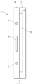
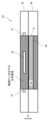
- FIG. 1 is a top view showing a configuration example of an optical module according to a first embodiment of the present invention
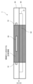
- 2 is a cross-sectional view for explaining details of the optical module according to the first embodiment of the present invention.
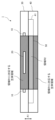
- FIG. FIG. 2 is a top view for explaining details of the optical module according to the first embodiment of the present invention.
- 2 is a cross-sectional view for explaining details of the optical module according to the first embodiment of the present invention.
- FIG. 2 is a cross-sectional view for explaining details of the optical module according to the first embodiment of the present invention.
- FIG. 2 is a cross-sectional view for explaining details of the optical module according to the first embodiment of the present invention.
- FIG. 11A and 11B are diagrams illustrating a modified example of the optical module in the first embodiment of the present invention.
- FIGS. 11A and 11B are diagrams illustrating a modified example of the optical module in the first embodiment of the present invention.
- 11A and 11B are diagrams illustrating a modified example of the optical module in the first embodiment of the present invention.
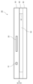
- FIG. 11 is a top view showing a configuration example of an optical module according to a second embodiment of the present invention.
- FIG. 11 is a cross-sectional view for explaining details of an optical module according to a second embodiment of the present invention.
- FIG. 11 is a cross-sectional view for explaining details of an optical module according to a second embodiment of the present invention.
- FIG. 1 is a perspective view showing an example of the configuration of the optical module 1.
- Fig. 2 is a cross-sectional view of the optical module 1. Specifically, Fig. 2 is a cross-sectional view of the optical module 1 taken along line AA' shown in Fig. 1.
- the optical module 1 includes a ring resonator 10, a heater 20, a first substrate 30, and a gap 50.
- the optical module 1 includes a ring resonator 10, a heater 20, a first substrate 30, a second substrate 40, and a gap 50.
- the ring resonator 10 has at least a ring-shaped optical waveguide 11.
- Light is incident on the ring-shaped optical waveguide 11 included in the ring resonator 10, and only light of a certain wavelength of the incident light is output from the ring-shaped optical waveguide 11.
- the wavelength of the output light is determined by the length of the ring-shaped optical waveguide 11 and the refractive index of the optical waveguide.
- the ring resonator 10 may further include a waveguide that guides light to be incident on the ring-shaped optical waveguide 11 and a waveguide that guides the light output from the ring-shaped optical waveguide 11 to another optical element.
- the heater 20 is provided inside the ring-shaped optical waveguide 11 included in the ring resonator 10. Specifically, the heater 20 is provided inside the first substrate 30 in a first region that has the ring-shaped optical waveguide 11 as its outer periphery when light passes through the first substrate 30 in a direction perpendicular to the surface of the first substrate 30. As shown in FIG. 2, the heater 20 is disposed at the same height as the ring resonator 10 in a direction perpendicular to the surface of the first substrate 30 (thickness direction of the first substrate 30 (up and down direction on the paper surface of FIG. 2)). The heights of the heater 20 and the ring resonator 10 may be different from each other.
- Figure 3 is a diagram in which the first region R1 is added to Figure 1 with diagonal lines.
- Figure 4 is a diagram in which the three-dimensional regions of the first substrate 30 and the second substrate 40 corresponding to the first region R1 are added to Figure 2 with diagonal lines.
- the three-dimensional region corresponding to the first region R1 refers to the region where the figure of the first region R1 extended in a direction perpendicular to the surface of the first substrate 30 overlaps with the first substrate 30 and the second substrate 40.
- the first region R1 has an outer periphery that is the shape of the ring-shaped optical waveguide 11 when light passes through the first substrate 30 from a direction perpendicular to the surface of the first substrate 30.
- the inner periphery of the ring-shaped optical waveguide 11 is the outer periphery of the first region R1, but the outer periphery of the ring-shaped optical waveguide may be the outer periphery of the first region R1.
- the three-dimensional region corresponding to the first region R1 has a columnar shape with the shape of the ring-shaped optical waveguide 11 as it passes through the first substrate 30 from a direction perpendicular to the surface of the first substrate 30 as its bottom surface.
- the three-dimensional region corresponding to the first region R1 is a region sandwiched between a part of one bottom surface of the first substrate 30 (the upper surface in FIG. 4) and a part of the other bottom surface of the first substrate 30 (the lower surface in FIG. 4). That is, in the examples shown in FIG. 1, FIG. 2, FIG. 3, and FIG. 4, the three-dimensional region corresponding to the first region R1 has a columnar shape with the shape of the ring-shaped optical waveguide 11 as its bottom surface on each of the two bottom surfaces of the first substrate 30.
- the heater 20 is disposed so that the distance from the bottom surface of the first substrate 30 (e.g., the top surface in Figures 2 and 4) is the same as the distance from the bottom surface of the first substrate 30 (e.g., the top surface in Figures 2 and 4) to the ring-shaped optical waveguide 11.
- the ring-shaped optical waveguide 11 and the heater 20 may be disposed so that these distances are different.
- the heater 20 generates heat in response to the power input from a drive circuit (not shown). As a result, the heater 20 heats the ring-shaped optical waveguide 11. Specifically, the heater 20 heats the first substrate 30 and the ring-shaped optical waveguide 11. Note that in the examples of Figures 1 and 3, the shape of the surface of the heater 20 when passing through the first substrate 30 from a direction perpendicular to the surface of the first substrate 30 is rectangular, but it may also be a polygon with more than a rectangle, an arc, a circle, or an ellipse.
- the second substrate 40 is a plate-like substrate that contains at least silicon, for example.
- the second substrate 40 is stacked in a first direction on the first substrate 30.
- the second substrate 40 also has a hole 41.
- the hole 41 is formed in the surface that contacts the first substrate 30 among the surfaces that constitute the second substrate 40.
- the second substrate 40 is bonded to the first substrate 30 via an area of the surface of the second substrate 40 that faces the first substrate 30 other than the area in which the hole 41 is provided.
- the void 50 is the space inside a hole provided on the surface of the second substrate 40 facing the first substrate 30.
- the void 50 is formed to include at least the region of the first region R1 that is located between the first substrate 30 and the second substrate 40 (second region R2, described below).
- the void 50 is filled with, for example, argon. The details of the void 50 will be described using Figures 5 and 6.
- FIG. 5 shows a portion of the three-dimensional region corresponding to the first region R1 shown in FIG. 4 as the second region R2.
- the second region R2 is a portion of the three-dimensional region corresponding to the first region R1 that is located between the first substrate 30 and the second substrate 40.
- FIG. 6 is a top view of the second substrate 40. As shown in FIG. 6, the second substrate 40 has a hole 41. Furthermore, the void 50 is a space located inside the hole 41. In this case, the hole 41 is formed such that the void 50 includes at least the second region R2.
- the second region R2 has a bottom surface whose outer periphery is the shape of the ring-shaped optical waveguide 11, similar to the three-dimensional region corresponding to the first region R1. Therefore, the second region R2 has a columnar shape whose bottom surface has the same shape as the ring-shaped optical waveguide 11, similar to the three-dimensional region corresponding to the first region R1.
- the distance between the two bottom surfaces in the second region R2 can be set arbitrarily.
- the optical module 1 includes a ring resonator 10, a heater 20, a first substrate 30, a second substrate 40, and a gap 50.
- the ring resonator 10 has a ring-shaped optical waveguide 11 and is attached to the first substrate 30.
- the heater 20 is provided inside the first substrate 30 within a first region R1 that has the optical waveguide 11 as its outer periphery when light passes through the first substrate 30 from a direction perpendicular to the surface of the first substrate 30, and heats the ring resonator 10.
- the second substrate 40 is laminated on the first substrate 30.
- the gap 50 is located between the first substrate 30 and the second substrate 40, and is formed so that the first substrate 30 and the second substrate 40 are spaced apart within the first region R1.
- the heat from the heater 20 is transferred to the second substrate 40 before reaching the ring-shaped optical waveguide 11. Therefore, the heat from the heater 20 cannot be efficiently transferred to the ring-shaped optical waveguide 11 (ring resonator structure).
- the optical module 1 has a gap formed in the first region R1 so that the first substrate 30 and the second substrate 40 are separated when passing through the first substrate 30 from a direction perpendicular to the surface of the first substrate 30.
- the first region R1 has the shape of the optical waveguide 11 as its outer periphery, so the gap 50 is formed in the region of the first substrate 30 where the first region R1 is located. Therefore, the heat from the heater 20 is not transmitted to the second substrate 40 until it is transmitted to the ring-shaped optical waveguide 11. As a result, the heat from the heater 20 can be efficiently transmitted to the ring-shaped optical waveguide (ring resonator structure). This allows the optical module 1 to suppress power consumption in the heater 20.
- the heater 20 is disposed at a position including the center of the first region R1 around the optical waveguide 11.
- a typical heater for heating an optical waveguide may be disposed near the optical waveguide in order to efficiently heat the optical waveguide.
- the gap 50 is formed, so the heater 20 can already efficiently heat the optical waveguide, and therefore the heater 20 may be disposed at a position including the center of the first region R1 around the optical waveguide 11. This eliminates the need to provide the heater 20 near the optical waveguide, improving the degree of freedom in the shape and position of the heater 20. This allows more freedom in determining the locations of other optical and electronic components in the optical module 1.
- the optical module 1A is a first modified example of the optical module 1.
- FIG. 7 is a diagram for explaining the optical module 1A.
- the optical module 1A includes a ring resonator 10, a heater 20, a first substrate 30, a second substrate 40, and a gap 50, similar to the optical module 1.
- the second substrate 40 does not have a hole 41
- the first substrate 30 has a hole 31.
- the gap 50 is a space formed inside the hole 31 of the first substrate 30.
- the first substrate 30 is bonded to the second substrate 40 through an area of the surface of the first substrate 30 facing the second substrate 40 other than the area where the hole 31 is provided.
- the optical module 1B is a second modified example of the optical module 1.
- FIG. 8 is a diagram for explaining the optical module 1B.
- the optical module 1B includes a ring resonator 10, a heater 20, a first substrate 30, a second substrate 40, and a gap 50, similar to the optical module 1.
- the optical module 1B further includes a third substrate 60.
- the third substrate 60 is stacked in a first direction with respect to the first substrate 30 and the second substrate 40.
- the first direction refers to the up-down direction indicated by the arrow A1 in FIG. 8.
- the second substrate 40 does not have a hole 41
- the third substrate 60 has a hole 61. Therefore, the gap 50 is a space formed inside the hole 61 of the third substrate 60.
- the optical module 1C is a third modified example of the optical module 1.
- FIG. 9 is a diagram for explaining the optical module 1C.
- the optical module 1C includes a ring resonator 10, a heater 20, a first substrate 30, a second substrate 40, and a gap 50, similar to the optical module 1.
- the first region R1 and the second region R2 are shown similar to FIG. 5.
- the gap 50 is shown to be larger than the second region R2.
- the gap 50 may be the same size as the second region R2, as shown in FIG. 9.
- Fig. 10 is a block diagram showing a configuration example of the optical module 2.
- Fig. 11 is a cross-sectional view of the optical module 2. Specifically, Fig. 11 is a cross-sectional view of the optical module 2 taken along line BB' shown in Fig. 10.
- Fig. 12 is a view in which a three-dimensional region corresponding to the first region R1 has been added to Fig. 11.
- the optical module 2 includes a ring resonator 10, a heater 20, a first substrate 30, and a gap 50.
- the optical module 1 includes a ring resonator 10, a heater 20, a first substrate 30, a second substrate 40, and a gap 50.
- the ring resonator 10 has a ring-shaped optical waveguide 11 and is attached to the first substrate 30.
- the heater 20 is provided in the first substrate 30 within a first region R1 that surrounds the optical waveguide 11 when light passes through the first substrate 30 from a direction perpendicular to the surface of the first substrate 30, and heats the ring resonator 10.
- the second substrate 40 is laminated on the first substrate 30.
- the gap 50 is located between the first substrate 30 and the second substrate 40, and is formed so that the first substrate 30 and the second substrate 40 are separated from each other within a three-dimensional region corresponding to the first region R1.
- the heat from the heater 20 is transferred to the second substrate 40 before reaching the ring-shaped optical waveguide 11. Therefore, the heat from the heater 20 cannot be efficiently transferred to the ring-shaped optical waveguide 11 (ring resonator structure).
- the optical module 2 has a gap formed so that the first substrate 30 and the second substrate 40 are separated in the first region R1 when passing through the first substrate 30 from a direction perpendicular to the surface of the first substrate 30.
- the first region R1 has the shape of the optical waveguide 11 as its outer periphery, so that the gap 50 is formed in the region of the first substrate 30 where the first region R1 is located. Therefore, the heat from the heater 20 is not transmitted to the second substrate 40 until it is transmitted to the ring-shaped optical waveguide 11. As a result, the heat from the heater 20 can be efficiently transmitted to the ring-shaped optical waveguide (ring resonator structure).
- a part or all of the above-mentioned embodiments can be described as follows, but are not limited to the following.
- (Appendix 1) A first substrate; a second substrate laminated on the first substrate; a ring resonator having a ring-shaped optical waveguide and attached to the first substrate; a heater provided inside the first substrate in a first region having an outer periphery around the optical waveguide when light passes through the first substrate in a direction perpendicular to a surface of the first substrate, the heater heating the ring resonator; a gap located between the first substrate and the second substrate, the gap being formed such that the first substrate and the second substrate are spaced apart within the first region; Equipped with Optical module.
Landscapes
- Physics & Mathematics (AREA)
- Engineering & Computer Science (AREA)
- Microelectronics & Electronic Packaging (AREA)
- General Physics & Mathematics (AREA)
- Optics & Photonics (AREA)
- Optical Modulation, Optical Deflection, Nonlinear Optics, Optical Demodulation, Optical Logic Elements (AREA)
- Optical Integrated Circuits (AREA)
Abstract
Description
第1の基板と、
前記第1の基板に対して積層される第2の基板と、
輪状の光導波路を有し、前記第1の基板に取り付けられたリング共振器と、
前記第1の基板の面に対して垂直な方向から前記第1の基板を透過した際に前記光導波路を外周とする第1の領域内であって、前記第1の基板の内部に設けられ、前記リング共振器を熱するヒータと、
前記第1の基板と前記第2の基板の間に位置し、前記第1の領域内で前記第1の基板と前記第2の基板が離間するように形成された空隙と、
を備える。
第1の実施形態における光モジュール1について、図1及び図2に基づき説明する。図1は、光モジュール1の構成例を示す透過図である。また、図2は、光モジュール1の断面図である。具体的には図2は、図1に示されるA-A’線で光モジュール1を断った場合の断面図である。
<第2の実施形態>
第2の実施形態に係る光モジュール2について、図10を用いて説明する。図10は、光モジュール2の構成例を示すブロック図である。また、図11は、光モジュール2の断面図である。具体的には図11は、図10に示されるB-B’線で光モジュール2を断った場合の断面図である。また、図12は、図11に第1の領域R1に対応する立体領域を追記したものである。
(付記1)
第1の基板と、
前記第1の基板に対して積層される第2の基板と、
輪状の光導波路を有し、前記第1の基板に取り付けられたリング共振器と、
前記第1の基板の面に対して垂直な方向から前記第1の基板を透過した際に前記光導波路を外周とする第1の領域内であって、前記第1の基板の内部に設けられ、前記リング共振器を熱するヒータと、
前記第1の基板と前記第2の基板の間に位置し、前記第1の領域内で前記第1の基板と前記第2の基板が離間するように形成された空隙と、
を備える、
光モジュール。
(付記2)
前記空隙は、前記第2の基板のうちで前記第1の基板と向かい合う面に設けられた穴の内側の空間であり、
前記第2の基板は、前記第2の基板のうちで前記第1の基板と向かい合う面のうちで前記穴が設けられた領域以外の領域を介して前記第1の基板と接着する、付記1に記載の光モジュール。
(付記3)
前記ヒータは、前記第1の領域内の中心部に配置される、付記1又は2の光モジュール。
(付記4)
前記空隙にはアルゴンが充填されている、付記1から3の何れか1項に記載の光モジュール。
(付記5)
前記第1の基板は石英ガラスを少なくとも含んで構成される、付記1から4の何れか1項に記載の光モジュール。
(付記6)
前記第2の基板はシリコンを少なくとも含んで構成される、付記1から5の何れか1項に記載の光モジュール。
10 リング共振器
11 光導波路
20 ヒータ
30 第1の基板
31 穴
40 第2の基板
41 穴
50 空隙
60 第3の基板
61 穴
R1 第1の領域
R2 第2の領域
Claims (6)
- 第1の基板と、
前記第1の基板に対して積層される第2の基板と、
輪状の光導波路を有し、前記第1の基板に取り付けられたリング共振器と、
前記第1の基板の面に対して垂直な方向から前記第1の基板を透過した際に前記光導波路を外周とする第1の領域内であって、前記第1の基板の内部に設けられ、前記リング共振器を熱するヒータと、
前記第1の基板と前記第2の基板の間に位置し、前記第1の領域内で前記第1の基板と前記第2の基板が離間するように形成された空隙と、
を備える、
光モジュール。 - 前記空隙は、前記第2の基板のうちで前記第1の基板と向かい合う面に設けられた穴の内側の空間であり、
前記第2の基板は、前記第2の基板のうちで前記第1の基板と向かい合う面のうちで前記穴が設けられた領域以外の領域を介して前記第1の基板と接着する、請求項1に記載の光モジュール。 - 前記ヒータは、前記第1の領域内の中心部に配置される、請求項1又は2に記載の光モジュール。
- 前記空隙にはアルゴンが充填されている、請求項1から3の何れか1項に記載の光モジュール。
- 前記第1の基板は石英ガラスを少なくとも含んで構成される、請求項1から4の何れか1項に記載の光モジュール。
- 前記第2の基板はシリコンを少なくとも含んで構成される、請求項1から5の何れか1項に記載の光モジュール。
Priority Applications (2)
| Application Number | Priority Date | Filing Date | Title |
|---|---|---|---|
| PCT/JP2023/004102 WO2024166232A1 (ja) | 2023-02-08 | 2023-02-08 | 光モジュール |
| JP2024575931A JPWO2024166232A1 (ja) | 2023-02-08 | 2023-02-08 |
Applications Claiming Priority (1)
| Application Number | Priority Date | Filing Date | Title |
|---|---|---|---|
| PCT/JP2023/004102 WO2024166232A1 (ja) | 2023-02-08 | 2023-02-08 | 光モジュール |
Publications (1)
| Publication Number | Publication Date |
|---|---|
| WO2024166232A1 true WO2024166232A1 (ja) | 2024-08-15 |
Family
ID=92262152
Family Applications (1)
| Application Number | Title | Priority Date | Filing Date |
|---|---|---|---|
| PCT/JP2023/004102 Ceased WO2024166232A1 (ja) | 2023-02-08 | 2023-02-08 | 光モジュール |
Country Status (2)
| Country | Link |
|---|---|
| JP (1) | JPWO2024166232A1 (ja) |
| WO (1) | WO2024166232A1 (ja) |
Citations (10)
| Publication number | Priority date | Publication date | Assignee | Title |
|---|---|---|---|---|
| JP2003084252A (ja) * | 2001-09-14 | 2003-03-19 | Hitachi Cable Ltd | 導波路型光部品及びその製造方法 |
| US20090245296A1 (en) * | 2008-04-01 | 2009-10-01 | Charles Santori | Tunable Optical Resonator |
| US20100054653A1 (en) * | 2008-08-29 | 2010-03-04 | Bae Systems Information And Electronic Systems Integration Inc. | Salicide structures for heat-influenced semiconductor applications |
| US20100247021A1 (en) * | 2009-03-31 | 2010-09-30 | Sun Microsystems, Inc. | Optical device with large thermal impedance |
| WO2011065384A1 (ja) * | 2009-11-25 | 2011-06-03 | シチズンホールディングス株式会社 | 光デバイス |
| US20110235962A1 (en) * | 2010-03-24 | 2011-09-29 | Oracle International Corporation | Optical device with high thermal tuning efficiency |
| JP2015519618A (ja) * | 2012-06-15 | 2015-07-09 | マイクロン テクノロジー, インク. | フォトニックデバイスを断熱する方法および装置 |
| JP2020095129A (ja) * | 2018-12-12 | 2020-06-18 | ルネサスエレクトロニクス株式会社 | 半導体装置およびその製造方法 |
| US20210109382A1 (en) * | 2019-10-09 | 2021-04-15 | Cisco Technology, Inc. | Thermal isolation element |
| JP2022061930A (ja) * | 2020-10-07 | 2022-04-19 | ジュニパー ネットワークス, インコーポレーテッド | ハイブリッドフォトニックリング変調器 |
-
2023
- 2023-02-08 JP JP2024575931A patent/JPWO2024166232A1/ja active Pending
- 2023-02-08 WO PCT/JP2023/004102 patent/WO2024166232A1/ja not_active Ceased
Patent Citations (10)
| Publication number | Priority date | Publication date | Assignee | Title |
|---|---|---|---|---|
| JP2003084252A (ja) * | 2001-09-14 | 2003-03-19 | Hitachi Cable Ltd | 導波路型光部品及びその製造方法 |
| US20090245296A1 (en) * | 2008-04-01 | 2009-10-01 | Charles Santori | Tunable Optical Resonator |
| US20100054653A1 (en) * | 2008-08-29 | 2010-03-04 | Bae Systems Information And Electronic Systems Integration Inc. | Salicide structures for heat-influenced semiconductor applications |
| US20100247021A1 (en) * | 2009-03-31 | 2010-09-30 | Sun Microsystems, Inc. | Optical device with large thermal impedance |
| WO2011065384A1 (ja) * | 2009-11-25 | 2011-06-03 | シチズンホールディングス株式会社 | 光デバイス |
| US20110235962A1 (en) * | 2010-03-24 | 2011-09-29 | Oracle International Corporation | Optical device with high thermal tuning efficiency |
| JP2015519618A (ja) * | 2012-06-15 | 2015-07-09 | マイクロン テクノロジー, インク. | フォトニックデバイスを断熱する方法および装置 |
| JP2020095129A (ja) * | 2018-12-12 | 2020-06-18 | ルネサスエレクトロニクス株式会社 | 半導体装置およびその製造方法 |
| US20210109382A1 (en) * | 2019-10-09 | 2021-04-15 | Cisco Technology, Inc. | Thermal isolation element |
| JP2022061930A (ja) * | 2020-10-07 | 2022-04-19 | ジュニパー ネットワークス, インコーポレーテッド | ハイブリッドフォトニックリング変調器 |
Also Published As
| Publication number | Publication date |
|---|---|
| JPWO2024166232A1 (ja) | 2024-08-15 |
Similar Documents
| Publication | Publication Date | Title |
|---|---|---|
| JP5050548B2 (ja) | 光モジュール | |
| CN101600983B (zh) | 热光型波导装置 | |
| CN102841404B (zh) | 平面型光波回路 | |
| US20110280512A1 (en) | Optical device | |
| JP2005521095A (ja) | 微細光変調器配列 | |
| JP7172184B2 (ja) | 光変調器、及びこれを用いた光モジュール | |
| WO2021199502A1 (ja) | 光制御素子とそれを用いた光変調デバイス並びに光送信装置 | |
| WO2019193706A1 (ja) | 光モジュール | |
| CN113424087B (zh) | 光模块 | |
| US7054524B2 (en) | Asymmetric photonic crystal waveguide element having symmetric mode fields | |
| US9063354B1 (en) | Passive thermo-optic feedback for robust athermal photonic systems | |
| WO2024166232A1 (ja) | 光モジュール | |
| US20140169739A1 (en) | Waveguide lens for coupling laser light source and optical element | |
| US20250180932A1 (en) | Optical waveguide element, and optical modulation device and optical transmission device using same | |
| JP2003322737A (ja) | 光導波路 | |
| WO2020245875A1 (ja) | 光導波路チップ | |
| WO2019117313A1 (ja) | 光偏波素子およびその製造方法 | |
| JP2020072116A (ja) | 光源装置 | |
| JP2020052269A (ja) | 光チップ、光集積回路及び光モジュール | |
| US11740491B2 (en) | Optical module and manufacturing method thereof | |
| JP3326761B2 (ja) | 周波数可変光源モジュール | |
| JP5320762B2 (ja) | 振動抑制構造 | |
| CN112639587A (zh) | 光调制器及使用了该光调制器的光模块 | |
| JP7852808B2 (ja) | 光導波路素子及びそれを用いた光変調器並びに光送信装置 | |
| JPH01214803A (ja) | 光方向性結合器 |
Legal Events
| Date | Code | Title | Description |
|---|---|---|---|
| 121 | Ep: the epo has been informed by wipo that ep was designated in this application |
Ref document number: 23921064 Country of ref document: EP Kind code of ref document: A1 |
|
| ENP | Entry into the national phase |
Ref document number: 2024575931 Country of ref document: JP Kind code of ref document: A |
|
| WWE | Wipo information: entry into national phase |
Ref document number: 2024575931 Country of ref document: JP |
|
| NENP | Non-entry into the national phase |
Ref country code: DE |
|
| 122 | Ep: pct application non-entry in european phase |
Ref document number: 23921064 Country of ref document: EP Kind code of ref document: A1 |