WO2024166200A1 - 電力変換器 - Google Patents
電力変換器 Download PDFInfo
- Publication number
- WO2024166200A1 WO2024166200A1 PCT/JP2023/003949 JP2023003949W WO2024166200A1 WO 2024166200 A1 WO2024166200 A1 WO 2024166200A1 JP 2023003949 W JP2023003949 W JP 2023003949W WO 2024166200 A1 WO2024166200 A1 WO 2024166200A1
- Authority
- WO
- WIPO (PCT)
- Prior art keywords
- power converter
- case
- circuit board
- heat
- space
- Prior art date
- Legal status (The legal status is an assumption and is not a legal conclusion. Google has not performed a legal analysis and makes no representation as to the accuracy of the status listed.)
- Ceased
Links
Images





Classifications
-
- H—ELECTRICITY
- H02—GENERATION; CONVERSION OR DISTRIBUTION OF ELECTRIC POWER
- H02M—APPARATUS FOR CONVERSION BETWEEN AC AND AC, BETWEEN AC AND DC, OR BETWEEN DC AND DC, AND FOR USE WITH MAINS OR SIMILAR POWER SUPPLY SYSTEMS; CONVERSION OF DC OR AC INPUT POWER INTO SURGE OUTPUT POWER; CONTROL OR REGULATION THEREOF
- H02M3/00—Conversion of DC power input into DC power output
Definitions
- This disclosure relates to a power converter.
- a power converter in which a heat-generating component such as a coil component is housed in a housing and the housing space is filled with a resin filler (see, for example, JP 2017-212774 A (Patent Document 1)).
- the power converter according to the present disclosure comprises a metal housing including a bottom wall portion and a side wall portion rising from the bottom wall portion so as to follow at least a portion of the outer edge of a first space, which is the space above the bottom wall portion; a circuit board disposed in the first space; a heat-generating component disposed in the first space and electrically connected to the circuit board; a case disposed apart from the circuit board in a top view of the circuit board, having an opening, and housing the heat-generating component; and a resin filler that fills the space between the case and the heat-generating component and has a first surface exposed at the opening.
- the heat-generating component includes a first terminal that protrudes in a direction intersecting a first plane that follows the first surface. The first terminal is electrically connected to the circuit board.
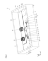
- FIG. 1 is a schematic perspective view showing a structure of a power converter according to a first embodiment.
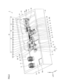
- FIG. 2 is a schematic perspective view showing the structure of the power converter according to the first embodiment.
- FIG. 3 is a schematic perspective view showing the case of FIG. 1 with the filler material therein omitted.
- FIG. 4 is a schematic plan view showing the structure of the power converter in the first embodiment.
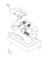
- FIG. 5 is a schematic exploded perspective view showing components of the power converter according to the first embodiment.
- FIG. 6 is a schematic plan view showing a state in which the heat-generating component is housed in the case.
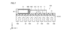
- FIG. 7 is a schematic cross-sectional view showing a structure in the vicinity of the case of the power converter according to the first embodiment.
- FIG. 1 is a schematic perspective view showing a structure of a power converter according to a first embodiment.
- FIG. 2 is a schematic perspective view showing the structure of the power converter according to the first embodiment.
- FIG. 3 is a schematic perspective view showing the case
- FIG. 8 is a schematic perspective view showing a state of connection between the terminals of the heat generating component and the bus bar.
- FIG. 9 is a schematic plan view showing an example of a connection between a bus bar and a terminal block.
- FIG. 10 is a schematic plan view showing a state in which a heat-generating component is accommodated in a case according to the second embodiment.
- FIG. 11 is a schematic plan view showing the structure of the power converter according to the third embodiment.
- FIG. 12 is a schematic cross-sectional view showing a structure in the vicinity of a case of a power converter according to the fourth embodiment.
- FIG. 13 is a schematic cross-sectional view showing a structure in the vicinity of a case of a power converter according to the fifth embodiment.
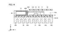
- FIG. 14 is a schematic cross-sectional view showing a structure in the vicinity of a case of a power converter according to the sixth embodiment.
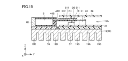
- FIG. 15 is a schematic cross-sectional view showing a structure in the vicinity of a case of a power converter according to the seventh embodiment.
- the power converter of the present disclosure includes a metal housing including a bottom wall and a side wall rising from the bottom wall along at least a part of the outer edge of a first space, which is a space above the bottom wall, a circuit board arranged in the first space, a heat generating component arranged in the first space and electrically connected to the circuit board, a case arranged apart from the circuit board in a top view of the circuit board, having an opening, and housing the heat generating component, and a resin filler having a first surface exposed at the opening, filling the space between the case and the heat generating component.
- the heat generating component includes a first terminal protruding in a direction intersecting a first plane along the first surface. The first terminal is electrically connected to the circuit board.
- the heat-generating components are housed in a case. This allows the heat-generating components to be housed in the case, and only the structure filled with filler can be placed in a heat treatment furnace or the like to harden the filler. As a result, it is possible to reduce the size of the structure to be placed in a heat treatment furnace or the like, improving production efficiency. In this way, the power converter disclosed herein can improve production efficiency.
- the case and filler may be arranged so that the first plane intersects with a second plane that is along the bottom surface, which is the surface of the bottom wall portion facing the first space.
- the first terminal may extend from inside the filler through the first surface to the outside of the case. This configuration makes it easy to seal the entire portion of the heat-generating component other than the terminal (main body) with the filler.
- the power converter may include multiple heat-generating components.
- the multiple heat-generating components may be housed in a case. In this way, housing multiple heat-generating components in one case improves the production efficiency of the power converter and makes it easier to reduce its size.
- the case may include a metal partition member that divides the internal space inside the case into a plurality of subspaces. At least one of the plurality of heat-generating components may be housed in one subspace.
- the multiple heat-generating components may include a first coil component and a second coil component.
- the first coil component may include a first coil and a first core through which magnetic flux formed by current flowing through the first coil passes.
- the second coil component may include a second coil and a second core through which magnetic flux formed by current flowing through the second coil passes.
- the direction of the magnetic flux passing through the first core may be different from the direction of the magnetic flux passing through the second core. In this way, by adjusting the orientation of the coil components, it becomes easy to reduce the space required to install a case that houses the multiple heat-generating components. As a result, it becomes easy to miniaturize the power converter.
- the multiple heat-generating components may include a transformer and an inductor.
- the space required to install the case can be reduced. As a result, it becomes easier to miniaturize the power converter.
- the multiple heat-generating components may include an inductor, a semiconductor device, and a capacitor.
- the space required to install the case can be reduced. As a result, it becomes easier to miniaturize the power converter.
- the power converter may further include a heat dissipation member disposed between the housing and the case so as to be in contact with the housing and the case.
- This configuration facilitates the transfer of heat from the case that houses the heat-generating component to the housing. As a result, it becomes easier to efficiently cool the heat-generating component.
- the case may include heat dissipation fins. This configuration makes it easier to efficiently cool the heat-generating components housed within the case.
- At least a portion of the outer wall surface of the case may surround at least a portion of the first space. This configuration allows the case to have the same function as the side wall of the housing. As a result, the structure of the power converter can be simplified.
- the case may be arranged to divide the first space into a plurality of element spaces. With this configuration, the case can prevent noise generated from a component installed in one element space from reaching components installed in other element spaces.
- the power converter may include multiple circuit boards.
- the case may be disposed so as to be sandwiched between the multiple circuit boards. With this configuration, the case can prevent noise generated from components installed on one circuit board from reaching components installed on other circuit boards.
- Fig. 1 is a schematic perspective view showing the structure of a power converter in the first embodiment.
- Fig. 2 is a schematic perspective view showing the power converter in the first embodiment as viewed from a different viewpoint than that in Fig. 1.
- Fig. 3 is a schematic perspective view showing Fig. 1 with the filler in the case omitted.
- Fig. 4 is a schematic plan view showing the structure of the power converter in the first embodiment.
- Fig. 5 is a schematic exploded perspective view showing the components of the power converter in the first embodiment disassembled.
- the power converter 1 in the first embodiment includes a housing 10, a first circuit board 31, a second circuit board 32, a third circuit board 33, a first heat dissipation sheet 37, a second heat dissipation sheet 38, a third heat dissipation sheet 39, a first heat generating component 51, a second heat generating component 52, a third heat generating component 53, a fourth heat generating component 54, a case 40, and fillers 46B, 47B, 48B, and 49B.
- the power converter 1 is a DC (Direct Current) DC converter.
- the power converter disclosed herein is not limited to a DCDC converter, and may be, for example, an inverter, a charger, etc.
- the housing 10 is made of metal.
- an aluminum alloy can be used as the metal constituting the housing 10.
- the housing 10 includes a bottom wall portion 19, a first side wall portion 11, a second side wall portion 12, a third side wall portion 13, and a fourth side wall portion 14.
- the housing 10 has a rectangular parallelepiped shape. More specifically, the housing 10 has a shape in which one face of a hollow rectangular parallelepiped has been removed.
- the bottom wall portion 19 has a flat plate shape.
- the bottom wall portion 19 has a rectangular shape.
- the long side direction of the bottom wall portion 19 is the X-axis direction
- the short side direction is the Y-axis direction
- the thickness direction of the bottom wall portion 19 is the Z-axis direction.
- the bottom wall portion 19 has a flat plate shape along the X-Y plane.
- the first side wall portion 11, the second side wall portion 12, the third side wall portion 13, and the fourth side wall portion 14 rise from the bottom wall portion 19 so as to follow the outer edge of the first space 10A, which is the space above the bottom wall portion 19.
- the first side wall portion 11, the second side wall portion 12, the third side wall portion 13, and the fourth side wall portion 14 each have a flat plate-like shape.
- the first side wall portion 11, the second side wall portion 12, the third side wall portion 13, and the fourth side wall portion 14 each have a rectangular shape.
- the first side wall portion 11 and the second side wall portion 12 rise vertically from the outer edge corresponding to the short side of the bottom wall portion 19.
- the third side wall portion 13 and the fourth side wall portion 14 rise vertically from the outer edge corresponding to the long side of the bottom wall portion 19.
- the first side wall portion 11 and the second side wall portion 12 face each other across the first space 10A.
- the third side wall 13 and the fourth side wall 14 face each other across the first space 10A.
- the first side wall 11 and the second side wall 12 have a flat plate shape along the Y-Z plane.
- the third side wall 13 and the fourth side wall 14 have a flat plate shape along the X-Z plane.
- the first side wall 11, the second side wall 12, the third side wall 13, and the fourth side wall 14 surround the first space 10A.
- the bottom wall 19 and the first side wall 11, the second side wall 12, the third side wall 13, and the fourth side wall 14 are integral with each other, but in other embodiments, they may be separate bodies (separate parts).
- the first circuit board 31, the second circuit board 32, and the third circuit board 33 are accommodated in the first space 10A of the housing 10.
- Each of the first circuit board 31, the second circuit board 32, and the third circuit board 33 includes a board body made of an insulator such as resin, and a circuit pattern (not shown) made of a conductor such as copper formed on the surface of the board body.
- the power converter 1 further includes devices 81 to 88, terminal blocks 71 to 74, and common mode choke coils 91 and 92. Devices 85, 86, 87, and 88 are installed on the first circuit board 31 (on the circuit pattern of the first circuit board 31).
- Terminal blocks 73 and 74 are further installed on the first circuit board 31 (on the circuit pattern of the first circuit board 31).
- Devices 81, 82, 83, and 84 are installed on the second circuit board 32 (on the circuit pattern of the second circuit board 32).
- Terminal blocks 71 and 72 are further provided on second circuit board 32 (on the circuit pattern of second circuit board 32).
- Common mode choke coils 91 and 92 are further provided on second circuit board 32 (on the circuit pattern of second circuit board 32).
- First circuit board 31 and second circuit board 32, as well as devices 81-88, terminal blocks 71-74, and common mode choke coils 91 and 92 provided on first circuit board 31 and second circuit board 32 constitute a switching circuit module.
- the power converter 1 further includes common mode choke coils 93, 94.
- the common mode choke coil 93 and the common mode choke coil 94 are installed on the third circuit board 33 (on the circuit pattern of the third circuit board 33).
- the third circuit board 33 and the common mode choke coils 93, 94 installed on the third circuit board 33 constitute a noise filter circuit module.
- FIG. 6 is a schematic plan view showing a state in which the heat generating component is accommodated in the case.
- the first heat generating component 51 is an inductor (first inductor) in this embodiment.
- the first heat generating component 51 includes a bobbin 51A, a coil 51B, a core 51C, and an inductor terminal 51D and an inductor terminal 51E as first terminals.
- the bobbin 51A has an annular shape.
- the coil 51B is wound around the outer circumferential surface of the bobbin 51A.
- the core 51C penetrates the bobbin 51A having an annular shape, thereby functioning as a core of the coil 51B.
- the inductor terminal 51D and the inductor terminal 51E are portions corresponding to both ends of the copper wire constituting the coil 51B.
- the inductor terminal 51D and the inductor terminal 51E are electrically and physically connected to the coil 51B.
- the second heat generating component 52 is a transformer.
- the second heat generating component 52 includes a bobbin 52A, a coil 52B, a core 52C, and transformer terminals 52D, 52E, 52F, and 52G as first terminals.
- the bobbin 52A has an annular shape.
- the coil 52B is wound around the outer circumferential surface of the bobbin 52A.
- the core 52C passes through the annular bobbin 52A and functions as the core of the coil 52B.
- the transformer terminals 52D, 52E, 52F, and 52G are electrically and physically connected to the coil 52B.
- the third heat generating component 53 is an inductor (second inductor).
- the third heat generating component 53 includes a bobbin 53A, a coil 53B, a core 53C, and inductor terminals 53D and 53E as first terminals.
- the bobbin 53A has an annular shape.
- the coil 53B is wound around the outer circumferential surface of the bobbin 53A.
- the core 53C penetrates the annular bobbin 53A to function as the core of the coil 53B.
- the inductor terminals 53D and 53E are portions that correspond to both ends of the copper wire that constitutes the coil 53B.
- the inductor terminals 53D and 53E are electrically and physically connected to the coil 53B.
- the fourth heat-generating component 54 is a reactor.
- the reactor has a known structure, and detailed description will be omitted here.
- the first heat generating component 51, the second heat generating component 52, the third heat generating component 53, and the fourth heat generating component 54 are coil components each including a coil.
- the first heat generating component 51 as the first coil component includes a coil 51B as the first coil, and a core 51C as the first core through which the magnetic flux formed by the current flowing through the coil 51B passes.
- the second heat generating component 52 as the second coil component includes a coil 52B as the second coil, and a core 52C as the second core through which the magnetic flux formed by the current flowing through the coil 52B passes.
- the third heat generating component 53 as the third coil component includes a coil 53B as the third coil, and a core 53C as the third core through which the magnetic flux formed by the current flowing through the coil 53B passes.
- the magnetic flux direction of the coil 51B, the magnetic flux direction of the coil 52B, and the magnetic flux direction of the coil 53B are all in the Z-axis direction.
- the coils 51B, 52B, and 53B have the same magnetic flux direction.
- the directions of the magnetic flux passing through cores 51C, 52C, and 53C are all in the X-axis direction.
- the directions of the magnetic flux passing through cores 51C, 52C, and 53C are the same.
- the power converter 1 further includes bus bars 61, 62, 63, 64, 65, and 66 as conductive members.
- the inductor terminal 51E of the first heat-generating component 51 is connected to the bus bar 61.
- the bus bar 61 is connected to the terminal block 71.
- the first heat-generating component 51 is electrically connected to the second circuit board 32.
- the inductor terminal 51D of the first heat-generating component 51 is connected to the bus bar 62.
- the bus bar 62 is connected to the transformer terminal 52D of the second heat-generating component 52.
- the first heat-generating component 51 is electrically connected to the second heat-generating component 52.
- the transformer terminal 52E of the second heat-generating component 52 is connected to the bus bar 63.
- the bus bar 63 is connected to the terminal block 72.
- the second heat-generating component 52 is electrically connected to the second circuit board 32.
- the transformer terminal 52F of the second heat-generating component 52 is connected to the bus bar 64.
- the bus bar 64 is connected to the terminal block 73.
- the second heat generating component 52 is electrically connected to the first circuit board 31.
- the transformer terminal 52G of the second heat generating component 52 is connected to the bus bar 65.
- the bus bar 65 is connected to the inductor terminal 53E of the third heat generating component 53.
- the second heat generating component 52 is electrically connected to the third heat generating component 53.
- the inductor terminal 53D of the third heat generating component 53 is connected to the bus bar 66.
- the bus bar 66 is connected to the terminal block 74.
- the third heat generating component 53 is electrically connected to the first circuit board 31.
- the fourth heat generating component 54 is electrically connected to the first circuit board 31 via a conductive member (not shown).
- the case 40 is disposed away from the first circuit board 31, the second circuit board 32, and the third circuit board 33 in a top view (viewed in the Z-axis direction) of the first circuit board 31, the second circuit board 32, and the third circuit board 33 (see FIG. 4).
- the case 40 is made of, for example, metal.
- the case 40 is separate from the housing 10.
- the case 40 includes a main body 41 and metal partition members 42, 43, and 44 that divide the internal space, which is the space inside the case (the space surrounded by the main body 41), into a plurality of partial spaces.
- the three partition members 42, 43, and 44 divide the internal space of the case 40 into four partial spaces, that is, partial space 46, partial space 47, partial space 48, and partial space 49.
- the case 40 has a plurality of openings 46A, 47A, 48A, and 49A (four in this embodiment).
- the first heat-generating component 51 is housed in the partial space 46.
- the second heat-generating component 52 is housed in the partial space 47.
- the third heat-generating component 53 is housed in the partial space 48.
- the fourth heat-generating component 54 is housed in the partial space 49. That is, one heat-generating component is housed in one partial space.
- the case 40, the first heat-generating component 51, the second heat-generating component 52, the third heat-generating component 53, and the fourth heat-generating component 54 constitute the heat-generating component module 20.
- the power converter 1 further includes heat dissipation sheets 37, 38, and 39 as heat dissipation members.
- the heat dissipation sheet 37 is located between the bottom wall 19 of the housing 10 and the first and second circuit boards 31 and 32, and is arranged so as to be in contact with the bottom wall 19 of the housing 10 and the first and second circuit boards 31 and 32.
- the heat dissipation sheet 38 is located between the bottom wall 19 of the housing 10 and the third circuit board 33, and is arranged so as to be in contact with the bottom wall 19 of the housing 10 and the third circuit board 33.
- the heat dissipation sheet 39 is located between the bottom wall 19 of the housing 10 and the case 40, and is arranged so as to be in contact with the bottom wall 19 of the housing 10 and the case 40.
- the power converter 1 includes a filler 46B, a filler 47B, a filler 48B, and a filler 49B.
- the fillers 46B, 47B, 48B, and 49B are made of resin.
- FIG. 7 is a schematic cross-sectional view showing a structure near the case of the power converter in the first embodiment.
- the filler 46B fills the space (partial space 46) between the case 40 and the first heat generating component 51, and has a surface 46C as a first surface exposed at the opening 46A.
- the filler 47B fills the space (partial space 47) between the case 40 and the second heat generating component 52, and has a surface 47C as a first surface exposed at the opening 47A.
- the filler 48B fills the space (partial space 48) between the case 40 and the third heat generating component 53, and has a surface 48C as a first surface exposed at the opening 48A.
- Filler 49B fills the space (partial space 49) between case 40 and fourth heat-generating component 54, and has surface 49C as a first surface exposed at opening 49A.
- a plurality of heat dissipation fins 19B are formed on the surface of bottom wall 19 of housing 10 opposite the surface facing first space 10A. This makes it easy to dissipate heat from housing 10 to the outside.
- inductor terminals 51D and 51E of first heat-generating component 51 protrude in a direction intersecting, or more specifically, in the Y-axis direction, which is a direction perpendicular to, the X-Z plane, which is a plane along surface 46C of filler 46B.
- Transformer terminals 52D, 52E, 52F and 52G of second heat-generating component 52 protrude in a direction intersecting, or more specifically, in the Y-axis direction, which is a direction perpendicular to, the X-Z plane, which is a plane along surface 47C of filler 47B.
- Inductor terminals 53D and 53E of third heat-generating component 53 protrude in a direction intersecting, or more specifically, in the Y-axis direction, which is a direction perpendicular to, the X-Z plane, which is a plane along surface 47C of filler 47B.
- the case 40 and fillers 46B, 47B, 48B, and 49B are arranged so that the X-Z plane, which is a plane along surface 46C of filler 46B, surface 47C of filler 47B, surface 48C of filler 48B, and surface 49C of filler 49B, intersects (more specifically, is perpendicular to) a second plane (X-Y plane) that is along bottom surface 19A, which is the surface of bottom wall portion 19 facing first space 10A.
- the X-Z plane which is a plane along surface 46C of filler 46B, surface 47C of filler 47B, surface 48C of filler 48B, and surface 49C of filler 49B
- Inductor terminals 51D and 51E of the first heat-generating component 51 extend from inside the filler 46B through surface 46C to the outside of the case 40.
- Transformer terminals 52D, 52E, 52F, and 52G of the second heat-generating component 52 extend from inside the filler 47B through surface 47C to the outside of the case 40.
- Inductor terminals 53D and 53E of the third heat-generating component 53 extend from inside the filler 48B through surface 48C to the outside of the case 40.
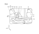
- FIG. 8 is a schematic perspective view showing the manner of connection between the terminal of the heat generating component and the bus bar.
- the bus bar 62 is disposed in an end region to be connected to the inductor terminal 51D of the first heat generating component 51, and includes a first region 621 extending in the Z-axis direction, which is a direction intersecting (more specifically, perpendicular to) the X-axis direction, which is a direction in which the portion other than the end region extends, a second region 622 extending in the Z-axis direction so as to face the first region 621, and a third region 623 connecting the first region 621 and the second region 622.
- the distance between the first region 621 and the third region 623 corresponds to the thickness of the inductor terminal 51D.
- the terminal block 71 includes a screw 71A and a main body 71B.
- the screw 71A is configured to be screwed into a screw hole (not shown) formed in the main body 71B and tightened to fix the bus bar 61 to the main body 71B.
- the bus bar 61 may have a structure capable of absorbing an error during assembly in the X-axis direction as described below.
- FIG. 9 is a schematic plan view showing an example of a manner of connection between the bus bar and the terminal block.
- the main body 71B of the terminal block 71 has a screw hole 71C extending in the thickness direction (Z-axis direction) of the second circuit board 32.
- the screw 71A is configured to be screwed into the screw hole 71C and tightened to fix the bus bar 61 to the main body 71B.
- the end of the bus bar 61 to be fixed to the terminal block 71 is bent so as to extend in the X-axis direction.
- An elongated hole 61A is formed at the end of the busbar 61, penetrating the busbar 61 in the thickness direction (Z-axis direction) and extending in the X-axis direction.
- the elongated hole 61A is a hole that is larger in the extension direction (X-axis direction) of the busbar 61 than in the width direction (Y-axis direction) of the busbar 61 when viewed in the thickness direction (Z-axis direction) of the second circuit board 32.
- the first heat generating component 51, the second heat generating component 52, the third heat generating component 53, and the fourth heat generating component 54 are housed in the case 40.
- the structure in which the heat generating components 51, 52, 53, and 54 are housed in the case 40 and filled with the fillers 46B, 47B, 48B, and 49B is put into a heat treatment furnace or the like to harden the fillers 46B, 47B, 48B, and 49B.
- the power converter 1 of this embodiment is a power converter that can improve production efficiency.
- the case 40 and the fillers 46B, 47B, 48B, 49B are arranged so that the plane (X-Z plane) along the surfaces 46C, 47C, 48C, 49C of the fillers 46B, 47B, 48B, 49B intersects (is perpendicular to) with the plane (X-Y plane) along the bottom surface 19A.
- the terminals 51D, 51E, 52D, 52E, 52F, 52G, 53D, and 53E of the heat-generating components 51, 52, and 53 extend from inside the fillers 46B, 47B, and 48B through the surfaces 46C, 47C, and 48C to the outside of the case 40. This makes it easy to seal the entire parts of the heat-generating components 51, 52, and 53 other than the terminals 51D, 51E, 52D, 52E, 52F, 52G, 53D, and 53E with the fillers 46B, 47B, and 48B.
- the power converter 1 of this embodiment contains multiple heat-generating components 51, 52, 53, and 54 in a single case 40, making it a power converter that can be easily produced with improved efficiency and made smaller.
- case 40 of this embodiment includes metal partition members 42, 43, and 44 that divide the internal space into multiple (four) partial spaces 46, 47, 48, and 49. This makes it possible to efficiently release heat from the heat-generating components 51, 52, 53, and 54 to the outside.
- the first heat-generating component 51, the second heat-generating component 52, the third heat-generating component 53, and the fourth heat-generating component 54 are an inductor, a transformer, an inductor, and a reactor, respectively.
- inductors, semiconductor devices, and capacitors may also be used as the first heat-generating component 51, the second heat-generating component 52, the third heat-generating component 53, and the fourth heat-generating component 54.
- housing these components, which may be arranged closely together, within a single case 40 it is possible to reduce the space required to install the case 40.
- the power converter 1 of this embodiment also includes a third heat dissipation sheet 39 as a heat dissipation member disposed between the housing 10 and the case 40 so as to be in contact with the housing 10 and the case 40. This facilitates the transfer of heat from the case 40, which houses the heat-generating components 51, 52, 53, and 54, to the housing 10, and the heat-generating components 51, 52, 53, and 54 are efficiently cooled.
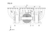
- Fig. 10 is a schematic plan view showing a state in which a heat-generating component is housed in a case in the second embodiment.
- Fig. 10 corresponds to Fig. 6 of the first embodiment.
- the power converter 1 of the second embodiment basically has the same structure as the power converter 1 of the first embodiment, and achieves the same effects. However, referring to FIG. 10 and FIG. 6, the structure of the heat generating component module 20 included in the power converter 1 of the second embodiment is different from that of the first embodiment.
- the direction of magnetic flux passing through core 52C as the second core is the X-axis direction, the same as in embodiment 1.
- the direction of magnetic flux passing through core 51C as the first core and core 53C as the third core is the Y-axis direction, unlike embodiment 1.
- the direction of magnetic flux passing through core 52C is different from the direction of magnetic flux passing through core 51C and the direction of magnetic flux passing through core 53C. More specifically, the direction of magnetic flux passing through core 52C is perpendicular to the direction of magnetic flux passing through core 51C and the direction of magnetic flux passing through core 53C.
- the power converter 1 of this embodiment is a power conversion device that can be easily miniaturized.
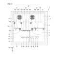
- Fig. 11 is a schematic plan view showing a structure of a power converter in the third embodiment.
- Fig. 11 corresponds to Fig. 4 of the first embodiment.
- the power converter 1 of the third embodiment basically has the same structure as the power converter 1 of the first embodiment, and achieves the same effects. However, referring to FIG. 11 and FIG. 4, the third embodiment differs from the first embodiment in the arrangement of the heat generating component module 20, the noise filter circuit module, and the switching circuit module.
- the case 40 is arranged so as to divide the first space 10A into a first element space 10B and a second element space 10C, which are a plurality of element spaces.
- a noise filter circuit module including a third circuit board 33 and common mode choke coils 93, 94 installed on the third circuit board 33 is arranged.
- the second element space 10C the first circuit board 31 and the second circuit board 32, as well as a switching circuit module including devices 81-88 and common mode choke coils 91, 92 installed on the first circuit board 31 and the second circuit board 32 are arranged.
- the case 40 is arranged so as to be sandwiched between the first circuit board 31 and the second circuit board 32 constituting the switching circuit module and the third circuit board 33 constituting the noise filter circuit module. This makes it possible for the case 40 to prevent noise generated by the components placed in the first element space 10B (components placed on the third circuit board 33) from reaching the components placed in the second element space 10C (components placed on the first circuit board 31 and the second circuit board 32).
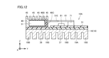
- Fig. 12 is a schematic cross-sectional view showing a structure in the vicinity of a case of a power converter in the fourth embodiment.
- Fig. 12 is a view corresponding to Fig. 7 of the first embodiment.
- the power converter 1 of the fourth embodiment basically has the same structure as the power converter 1 of the first embodiment, and has the same effects. However, referring to Figs. 12 and 7, the structure of the case 40 of the fourth embodiment is different from that of the first embodiment.
- the case 40 of the fourth embodiment includes heat dissipation fins 45.
- the heat dissipation fins 45 are formed on the surface of the case 40 opposite the surface facing the bottom wall portion 19 in the thickness direction (Z-axis direction) of the bottom wall portion 19.
- the case 40 including the heat dissipation fins 45 it is possible to efficiently cool the heat-generating components 51, 52, 53, and 54 housed within the case 40.
- Fig. 13 is a schematic cross-sectional view showing a structure in the vicinity of a case of a power converter in the fifth embodiment.
- Fig. 13 is a view corresponding to Fig. 7 of the first embodiment.
- the power converter 1 of the fifth embodiment basically has the same structure as the power converter 1 of the first embodiment, and achieves the same effects. However, referring to Figs. 13 and 7, the fifth embodiment differs from the first embodiment in the structure of the housing 10 and the case 40.
- outer wall surface 40C which is a part of the outer wall surface of case 40 of embodiment 5, surrounds a part of first space 10A.
- case 40 of embodiment 5 functions as a part of housing 10 (side wall portion of housing 10).
- Housing 10 includes a plurality of heat dissipation fins 45.
- Fig. 14 is a schematic cross-sectional view showing a structure in the vicinity of a case of a power converter in the sixth embodiment.
- Fig. 14 is a view corresponding to Fig. 7 of the first embodiment.
- the power converter 1 of the sixth embodiment basically has the same structure as the power converter 1 of the first embodiment, and achieves the same effects. However, referring to Figs. 14 and 7, the sixth embodiment differs from the first embodiment in that the power converter 1 further includes a fourth circuit board 34.
- the power converter 1 in the sixth embodiment further includes a fourth circuit board 34.
- On the fourth circuit board 34 there are mounted elements (not shown) for controlling the first circuit board 31 and the second circuit board 32, as well as the devices 81 to 88 mounted on the first circuit board 31 and the second circuit board 32, and a switching circuit module including the common mode choke coils 91 and 92.
- the fourth circuit board 34 constitutes a control circuit module. At least a portion of the inductor terminal 51E and the bus bar 61 is located between the fourth circuit board 34 and the first circuit board 31. In this way, by adopting a structure in which the multiple circuit boards at least partially overlap in the thickness direction (Z-axis direction) of the bottom wall portion 19, the first space 10A can be effectively utilized. As a result, the power converter 1 in the sixth embodiment is a power converter that can be easily made compact.
- Fig. 15 is a schematic cross-sectional view showing a structure in the vicinity of a case of a power converter in the seventh embodiment.
- Fig. 15 is a view corresponding to Fig. 14 of the sixth embodiment.
- the power converter 1 of the seventh embodiment basically has the same structure as the power converter 1 of the sixth embodiment, and has the same effects. However, referring to Figs. 15 and 14, the seventh embodiment differs from the sixth embodiment in that the terminals and bus bars of the heat generating components have an insulating coating.
- inductor terminal 51E in the seventh embodiment includes insulating coating 511 covering its surface.
- Bus bar 61 includes insulating coating 611 covering its surface. Since inductor terminal 51E and bus bar 61 include insulating coatings 511, 611, it is possible to reduce the insulation distance between inductor terminal 51E and bus bar 61 and other members. This makes it possible to reduce, for example, distance D1 between inductor terminal 51E and bus bar 61 and fourth circuit board 34, and distance D2 between inductor terminal 51E and bus bar 61 and device 81. As a result, power converter 1 in the seventh embodiment is a power converter that can be easily made compact, particularly in the Z-axis direction.
Landscapes
- Engineering & Computer Science (AREA)
- Power Engineering (AREA)
- Dc-Dc Converters (AREA)
Abstract
Description
一般に、発熱部品を収容するための収容空間を充填する樹脂製の充填材を硬化させるためには、熱処理が必要である。特許文献1に開示されているように収容空間を規定する収容部と回路基板とが接続される構造では、充填材の硬化のための熱処理に際して、収容部以外の領域を含む大きな構造体を熱処理炉等に投入して熱処理を実施する必要がある。その結果、生産効率の向上が難しいという問題がある。本開示の目的の1つは、生産効率の向上が可能な電力変換器を提供することである。
本開示の電力変換器によれば、生産効率を向上させることができる。
最初に本開示の実施態様を列記して説明する。本開示の電力変換器は、底壁部と、底壁部上の空間である第1空間の外縁の少なくとも一部に沿うように底壁部から立ち上がる側壁部と、を含む金属製の筐体と、第1空間内に配置された回路基板と、第1空間内に配置され、回路基板と電気的に接続された発熱部品と、回路基板の上面視において回路基板と離れて配置され、開口部を有し、発熱部品を収容するケースと、ケースと発熱部品との間の空間を充填し、開口部において露出する第1表面を有する樹脂製の充填材と、を備える。発熱部品は、第1表面に沿う第1平面に対して交差する方向に突出する第1端子を含む。第1端子と回路基板とが電気的に接続されている。
次に、本開示にかかる電力変換器の実施の形態を、以下に図面を参照しつつ説明する。なお、以下の図面において同一または相当する部分には同一の参照番号を付しその説明は繰返さない。
まず、本開示の一実施の形態である実施の形態1について説明する。図1は、実施の形態1における電力変換器の構造を示す概略斜視図である。図2は、実施の形態1における電力変換器を、図1とは異なる視点から見た状態を示す概略斜視図である。図3は、図1において、ケース内の充填材を省略して示す概略斜視図である。図4は、実施の形態1における電力変換器の構造を示す概略平面図である。図5は、実施の形態1における電力変換器の部品を分解して示す概略分解斜視図である。
筐体10は、金属製である。筐体10を構成する金属としては、たとえばアルミニウム合金を採用することができる。筐体10は、底壁部19と、第1側壁部11と、第2側壁部12と、第3側壁部13と、第4側壁部14とを含んでいる。筐体10は、直方体状の形状を有している。より具体的には、中空の直方体の一の面が除去された形状を有している。底壁部19は平板状の形状を有している。底壁部19は、長方形状の形状を有している。実施の形態1~7において、底壁部19の長辺方向はX軸方向、短辺方向はY軸方向、底壁部19の厚み方向はZ軸方向である。底壁部19は、X-Y平面に沿う平板状の形状を有している。
第1回路基板31、第2回路基板32および第3回路基板33は、筐体10の第1空間10A内に収容されている。第1回路基板31、第2回路基板32および第3回路基板33のそれぞれは、樹脂などの絶縁体からなる基板本体と、基板本体の表面に形成された銅などの導電体製の回路パターン(図示しない)とを含んでいる。電力変換器1は、デバイス81~88、端子台71~74およびコモンモードチョークコイル91,92をさらに備えている。第1回路基板31上(第1回路基板31の回路パターン上)には、デバイス85と、デバイス86と、デバイス87と、デバイス88とが設置されている。第1回路基板31上(第1回路基板31の回路パターン上)には、さらに端子台73と、端子台74とが設置されている。第2回路基板32上(第2回路基板32の回路パターン上)には、デバイス81と、デバイス82と、デバイス83と、デバイス84とが設置されている。第2回路基板32上(第2回路基板32の回路パターン上)には、さらに端子台71と、端子台72とが設置されている。第2回路基板32上(第2回路基板32の回路パターン上)には、さらにコモンモードチョークコイル91と、コモンモードチョークコイル92とが設置されている。第1回路基板31および第2回路基板32、ならびに第1回路基板31および第2回路基板32上に設置されるデバイス81~88、端子台71~74、コモンモードチョークコイル91,92は、スイッチング回路モジュールを構成する。
図6は、ケース内に発熱部品が収容された状態を示す概略平面図である。図6および図3を参照して、第1発熱部品51は、本実施の形態においてはインダクタ(第1インダクタ)である。第1発熱部品51は、ボビン51Aと、コイル51Bと、コア51Cと、第1端子としてのインダクタ端子51Dおよびインダクタ端子51Eとを含んでいる。ボビン51Aは、環状の形状を有している。コイル51Bは、ボビン51Aの外周面に巻き付けられている。コア51Cは、環状の形状を有するボビン51Aを貫通することにより、コイル51Bのコアとして機能する。インダクタ端子51Dおよびインダクタ端子51Eは、コイル51Bを構成する銅線の両端に対応する部分である。インダクタ端子51Dおよびインダクタ端子51Eは、コイル51Bに電気的かつ物理的に接続されている。
図5および図7を参照して、電力変換器1は、放熱部材としての放熱シート37,38,39をさらに備えている。放熱シート37は、筐体10の底壁部19と第1回路基板31および第2回路基板32との間に位置して、筐体10の底壁部19と第1回路基板31および第2回路基板32とに接触するように配置されている。放熱シート38は、筐体10の底壁部19と第3回路基板33との間に位置して、筐体10の底壁部19と第3回路基板33とに接触するように配置されている。放熱シート39は、筐体10の底壁部19とケース40との間に位置して、筐体10の底壁部19とケース40とに接触するように配置されている。
図1を参照して、電力変換器1は、充填材46Bと、充填材47Bと、充填材48Bと、充填材49Bとを備えている。充填材46B、充填材47B、充填材48Bおよび充填材49Bは、樹脂製である。図7は、実施の形態1における電力変換器のケース付近の構造を示す概略断面図である。図7および図1を参照して、充填材46Bは、ケース40と第1発熱部品51との間の空間(部分空間46)を充填し、開口部46Aにおいて露出する第1表面としての表面46Cを有している。充填材47Bは、ケース40と第2発熱部品52との間の空間(部分空間47)を充填し、開口部47Aにおいて露出する第1表面としての表面47Cを有している。充填材48Bは、ケース40と第3発熱部品53との間の空間(部分空間48)を充填し、開口部48Aにおいて露出する第1表面としての表面48Cを有している。充填材49Bは、ケース40と第4発熱部品54との間の空間(部分空間49)を充填し、開口部49Aにおいて露出する第1表面としての表面49Cを有している。図7を参照して、筐体10の底壁部19の第1空間10Aに面する表面とは反対の表面には、複数の放熱フィン19Bが形成されている。これにより、筐体10の熱を外部へと放出することが容易となっている。
次に、発熱部品の端子とバスバーとの接続の態様について説明する。図8は、発熱部品の端子とバスバーとの接続の態様を示す概略斜視図である。図8を参照して、バスバー62は、第1発熱部品51のインダクタ端子51Dと接続されるべき端部領域に配置され、端部領域以外の部分が延びる方向であるX軸方向に対して交差する方向(より具体的には直交する方向)であるZ軸方向に延びる第1領域621と、第1領域621に向かい合うようにZ軸方向に延びる第2領域622と、第1領域621と第2領域622とを接続する第3領域623とを含んでいる。第1領域621と第3領域623との間隔は、インダクタ端子51Dの太さに対応する間隔とされている。第1領域621、第2領域622および第3領域623を含むこのような屈曲領域をバスバー62の端部に形成しておくことにより、インダクタ端子51Dの延びる方向(Y軸方向)における組み立て時の誤差を吸収することができる。その結果、電力変換器1の組み立てが容易となっている。本実施の形態においては、発熱部品の端子と接続されるバスバーの全ての端部に、上記屈曲構造が採用されている。
次に、バスバーと端子台との接続の態様について説明する。図1を参照して、端子台71は、ねじ71Aと、本体71Bとを含んでいる。ねじ71Aは、本体71Bに形成されたねじ穴(図示しない)にねじ込まれ、締め付けられることにより、本体71Bに対してバスバー61を固定可能に構成されている。ここで、バスバー61は、以下のようにX軸方向における組み立て時の誤差を吸収することが可能な構造を有していてもよい。図9は、バスバーと端子台との接続の態様の一例を示す概略平面図である。端子台71の本体71Bは、第2回路基板32の厚み方向(Z軸方向)に延びるねじ穴71Cを有している。ねじ71Aは、ねじ穴71Cにねじ込まれ、締め付けられることにより、本体71Bに対してバスバー61を固定可能に構成されている。図9を参照して、端子台71に対して固定されるべきバスバー61の端部はX軸方向に延びるように屈曲している。バスバー61の端部には、バスバー61を厚み方向(Z軸方向)に貫通し、X軸方向に延びる長孔61Aが形成されている。長孔61Aは、第2回路基板32の厚み方向(Z軸方向)に見て、バスバー61の幅方向(Y軸方向)に比べてバスバー61の延びる方向(X軸方向)において大きい穴である。このような長孔61Aをバスバー61に形成することにより、長孔61Aの延びる方向(X軸方向)における組み立て時の誤差を吸収することができる。その結果、電力変換器1の組み立てを容易にすることができる。
本実施の形態の電力変換器1においては、第1発熱部品51、第2発熱部品52、第3発熱部品53および第4発熱部品54が、ケース40に収容されている。これにより、ケース40に発熱部品51,52,53,54を収容し、充填材46B,47B,48B,49Bを充填した構造体のみを熱処理炉等に投入して充填材46B,47B,48B,49Bを硬化させることができる。その結果、熱処理炉等に投入すべき構造体を小さくすることが可能となり、生産効率を向上させることができる。このように、本実施の形態の電力変換器1は、生産効率を向上させることが可能な電力変換器となっている。
次に、本開示の他の実施の形態である実施の形態2について説明する。図10は、実施の形態2におけるケース内に発熱部品が収容された状態を示す概略平面図である。図10は、実施の形態1の図6に対応する図である。
次に、本開示のさらに他の実施の形態である実施の形態3について説明する。図11は、実施の形態3における電力変換器の構造を示す概略平面図である。図11は、実施の形態1の図4に対応する図である。
次に、本開示のさらに他の実施の形態である実施の形態4について説明する。図12は、実施の形態4における電力変換器のケース付近の構造を示す概略断面図である。図12は、実施の形態1の図7に対応する図である。
次に、本開示のさらに他の実施の形態である実施の形態5について説明する。図13は、実施の形態5における電力変換器のケース付近の構造を示す概略断面図である。図13は、実施の形態1の図7に対応する図である。
次に、本開示のさらに他の実施の形態である実施の形態6について説明する。図14は、実施の形態6における電力変換器のケース付近の構造を示す概略断面図である。図14は、実施の形態1の図7に対応する図である。
次に、本開示のさらに他の実施の形態である実施の形態7について説明する。図15は、実施の形態7における電力変換器のケース付近の構造を示す概略断面図である。図15は、実施の形態6の図14に対応する図である。
Claims (13)
- 底壁部と、前記底壁部上の空間である第1空間の外縁の少なくとも一部に沿うように前記底壁部から立ち上がる側壁部と、を含む金属製の筐体と、
前記第1空間内に配置された回路基板と、
前記第1空間内に配置され、前記回路基板と電気的に接続された発熱部品と、
前記回路基板の上面視において前記回路基板と離れて配置され、開口部を有し、前記発熱部品を収容するケースと、
前記ケースと前記発熱部品との間の空間を充填し、前記開口部において露出する第1表面を有する樹脂製の充填材と、を備え、
前記発熱部品は、前記第1表面に沿う第1平面に対して交差する方向に突出する第1端子を含み、
前記第1端子と前記回路基板とが電気的に接続されている、電力変換器。 - 前記第1平面と、前記第1空間に面する前記底壁部の表面である底面に沿う第2平面とが交差するように前記ケースおよび前記充填材は配置される、請求項1に記載の電力変換器。
- 前記第1端子は、前記充填材の内部から前記第1表面を貫通して前記ケースの外部にまで延びる、請求項1または請求項2に記載の電力変換器。
- 前記電力変換器は、複数の前記発熱部品を備え、
前記複数の発熱部品は、前記ケースに収容される、請求項1から請求項3のいずれか1項に記載の電力変換器。 - 前記ケースは、前記ケース内部の空間である内部空間を複数の部分空間に仕切る金属製の仕切り部材を含み、
前記複数の発熱部品の少なくとも1つは、1つの前記部分空間に収容される、請求項4に記載の電力変換器。 - 前記複数の発熱部品は、
第1コイル部品と、
第2コイル部品と、を含み、
前記第1コイル部品は、
第1コイルと、
前記第1コイルを流れる電流によって形成される磁束が通過する第1コアと、を含み、
前記第2コイル部品は、
第2コイルと、
前記第2コイルを流れる電流によって形成される磁束が通過する第2コアと、を含み、
前記回路基板の上面視において、前記第1コアを通過する磁束の方向と前記第2コアを通過する磁束の方向とが異なる、請求項4または請求項5に記載の電力変換器。 - 前記複数の発熱部品は、トランスおよびインダクタを含む、請求項4から請求項6のいずれか1項に記載の電力変換器。
- 前記複数の発熱部品は、インダクタ、半導体デバイスおよびコンデンサを含む、請求項4から請求項6のいずれか1項に記載の電力変換器。
- 前記電力変換器は、前記筐体と前記ケースとの間に前記筐体および前記ケースと接触するように配置された放熱部材をさらに備える、請求項1から請求項8のいずれか1項に記載の電力変換器。
- 前記ケースは放熱フィンを含む、請求項1から請求項9のいずれか1項に記載の電力変換器。
- 前記ケースの外壁面の少なくとも一部は、前記第1空間の少なくとも一部を取り囲む、請求項1から請求項10のいずれか1項に記載の電力変換器。
- 前記ケースは、前記第1空間を複数の要素空間に仕切るように配置される、請求項1から請求項11のいずれか1項に記載の電力変換器。
- 前記電力変換器は、複数の前記回路基板を備え、
前記ケースは、前記複数の回路基板の間に挟まれるように配置される、請求項1から請求項12のいずれか1項に記載の電力変換器。
Priority Applications (2)
| Application Number | Priority Date | Filing Date | Title |
|---|---|---|---|
| JP2024575904A JP7782733B2 (ja) | 2023-02-07 | 2023-02-07 | 電力変換器 |
| PCT/JP2023/003949 WO2024166200A1 (ja) | 2023-02-07 | 2023-02-07 | 電力変換器 |
Applications Claiming Priority (1)
| Application Number | Priority Date | Filing Date | Title |
|---|---|---|---|
| PCT/JP2023/003949 WO2024166200A1 (ja) | 2023-02-07 | 2023-02-07 | 電力変換器 |
Publications (1)
| Publication Number | Publication Date |
|---|---|
| WO2024166200A1 true WO2024166200A1 (ja) | 2024-08-15 |
Family
ID=92262128
Family Applications (1)
| Application Number | Title | Priority Date | Filing Date |
|---|---|---|---|
| PCT/JP2023/003949 Ceased WO2024166200A1 (ja) | 2023-02-07 | 2023-02-07 | 電力変換器 |
Country Status (2)
| Country | Link |
|---|---|
| JP (1) | JP7782733B2 (ja) |
| WO (1) | WO2024166200A1 (ja) |
Citations (3)
| Publication number | Priority date | Publication date | Assignee | Title |
|---|---|---|---|---|
| JP2003332526A (ja) * | 2001-11-07 | 2003-11-21 | Hitachi Ltd | 電力変換装置 |
| JP2019029485A (ja) * | 2017-07-28 | 2019-02-21 | パナソニックIpマネジメント株式会社 | 電源装置 |
| JP2020061890A (ja) * | 2018-10-12 | 2020-04-16 | パナソニックIpマネジメント株式会社 | 電力変換装置 |
Family Cites Families (1)
| Publication number | Priority date | Publication date | Assignee | Title |
|---|---|---|---|---|
| JP2602612Y2 (ja) * | 1993-02-13 | 2000-01-24 | ティーディーケイ株式会社 | 電源装置 |
-
2023
- 2023-02-07 JP JP2024575904A patent/JP7782733B2/ja active Active
- 2023-02-07 WO PCT/JP2023/003949 patent/WO2024166200A1/ja not_active Ceased
Patent Citations (3)
| Publication number | Priority date | Publication date | Assignee | Title |
|---|---|---|---|---|
| JP2003332526A (ja) * | 2001-11-07 | 2003-11-21 | Hitachi Ltd | 電力変換装置 |
| JP2019029485A (ja) * | 2017-07-28 | 2019-02-21 | パナソニックIpマネジメント株式会社 | 電源装置 |
| JP2020061890A (ja) * | 2018-10-12 | 2020-04-16 | パナソニックIpマネジメント株式会社 | 電力変換装置 |
Also Published As
| Publication number | Publication date |
|---|---|
| JPWO2024166200A1 (ja) | 2024-08-15 |
| JP7782733B2 (ja) | 2025-12-09 |
Similar Documents
| Publication | Publication Date | Title |
|---|---|---|
| CN110521100B (zh) | 电力转换装置用滤波器模块 | |
| JP6234537B1 (ja) | 電力変換装置 | |
| JP4802615B2 (ja) | Lc複合部品 | |
| JP6525360B1 (ja) | 電力変換装置 | |
| US12614661B2 (en) | Transformer and flat panel display device including same | |
| JP7727731B2 (ja) | 電子部品モジュールおよびこれを含む電源供給装置 | |
| JP6903156B2 (ja) | 電力変換装置 | |
| US20220264769A1 (en) | Power converter and method for manufacturing power converter | |
| JP2008098209A (ja) | コイルの絶縁構造 | |
| US20240062942A1 (en) | Coil device | |
| JP6516910B1 (ja) | 降圧コンバータ | |
| US20220215997A1 (en) | Power Conversion Device | |
| JP2000150250A (ja) | コイル部品とその取付構造 | |
| JP7782733B2 (ja) | 電力変換器 | |
| WO2020153164A1 (ja) | 回路構成体、電気接続箱及び回路構成体の製造方法 | |
| JP6575380B2 (ja) | コイル部品及び電源装置 | |
| JP7338434B2 (ja) | 電気装置 | |
| JP6651592B1 (ja) | リアクトルの冷却構造、及び電力変換装置 | |
| JP7629067B1 (ja) | 絶縁型コンバータ | |
| JP7574949B1 (ja) | トランスおよび電力変換装置 | |
| JP7148376B2 (ja) | リアクトル | |
| JP7834761B2 (ja) | 電子部品モジュールおよびこれを含む電源供給装置 | |
| JP4802616B2 (ja) | Lc複合部品 | |
| JP2026059793A (ja) | コンバータユニット | |
| JP2025002424A (ja) | インダクタおよび部品実装モジュール |
Legal Events
| Date | Code | Title | Description |
|---|---|---|---|
| 121 | Ep: the epo has been informed by wipo that ep was designated in this application |
Ref document number: 23921036 Country of ref document: EP Kind code of ref document: A1 |
|
| ENP | Entry into the national phase |
Ref document number: 2024575904 Country of ref document: JP Kind code of ref document: A |
|
| WWE | Wipo information: entry into national phase |
Ref document number: 2024575904 Country of ref document: JP |
|
| NENP | Non-entry into the national phase |
Ref country code: DE |
|
| 122 | Ep: pct application non-entry in european phase |
Ref document number: 23921036 Country of ref document: EP Kind code of ref document: A1 |