WO2024162456A1 - 光電気配線基板 - Google Patents
光電気配線基板 Download PDFInfo
- Publication number
- WO2024162456A1 WO2024162456A1 PCT/JP2024/003403 JP2024003403W WO2024162456A1 WO 2024162456 A1 WO2024162456 A1 WO 2024162456A1 JP 2024003403 W JP2024003403 W JP 2024003403W WO 2024162456 A1 WO2024162456 A1 WO 2024162456A1
- Authority
- WO
- WIPO (PCT)
- Prior art keywords
- cladding layer
- optical
- electrical wiring
- optical waveguide
- waveguide core
- Prior art date
- Legal status (The legal status is an assumption and is not a legal conclusion. Google has not performed a legal analysis and makes no representation as to the accuracy of the status listed.)
- Ceased
Links
Images



Classifications
-
- G—PHYSICS
- G02—OPTICS
- G02B—OPTICAL ELEMENTS, SYSTEMS OR APPARATUS
- G02B6/00—Light guides; Structural details of arrangements comprising light guides and other optical elements, e.g. couplings
- G02B6/10—Light guides; Structural details of arrangements comprising light guides and other optical elements, e.g. couplings of the optical waveguide type
- G02B6/12—Light guides; Structural details of arrangements comprising light guides and other optical elements, e.g. couplings of the optical waveguide type of the integrated circuit kind
- G02B6/122—Basic optical elements, e.g. light-guiding paths
-
- H—ELECTRICITY
- H05—ELECTRIC TECHNIQUES NOT OTHERWISE PROVIDED FOR
- H05K—PRINTED CIRCUITS; CASINGS OR CONSTRUCTIONAL DETAILS OF ELECTRIC APPARATUS; MANUFACTURE OF ASSEMBLAGES OF ELECTRICAL COMPONENTS
- H05K1/00—Printed circuits
- H05K1/02—Details
Definitions
- the disclosed embodiment relates to an optical-electrical wiring board.
- optical-electrical wiring boards have been disclosed in which optical waveguide cores and electrical wiring are arranged on the same layer for the purpose of parallel transmission of optical signals and electrical signals (see, for example, Patent Document 1).
- the optical-electrical wiring board includes an optical waveguide core that transmits an optical signal, and a second clad layer that covers at least the side surface of the optical waveguide core.
- the surface of the second clad layer also has a convex portion located around the optical waveguide core.
- FIG. 1 is a cross-sectional view showing an example of a configuration of an optical-electrical wiring board according to an embodiment.
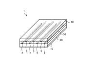
- FIG. 2 is a perspective view showing an example of a configuration of an optical-electrical wiring board according to the embodiment.
- FIG. 3 is a cross-sectional view showing an example of the configuration of an optical-electrical wiring board according to another embodiment 1.
- FIG. 4 is a cross-sectional view showing an example of the configuration of an optical-electrical wiring board according to another embodiment 2.
- FIG. 5 is a cross-sectional view showing an example of the configuration of an optical-electrical wiring board according to another embodiment 3.
- FIG. 4 is a cross-sectional view showing an example of the configuration of an optical-electrical wiring board according to another embodiment 2.
- optical-electrical wiring boards have been disclosed in which optical waveguide cores and electrical wiring are arranged on the same layer for the purpose of parallel transmission of optical signals and electrical signals.
- the optical waveguide core is surrounded by a layered cladding layer, so the optical signal leaking out of the optical waveguide core may have difficulty returning to the optical waveguide core. This may result in a deterioration in the propagation characteristics of the optical signal.
- FIG. 1 is a cross-sectional view showing an example of the configuration of an optical-electrical wiring board 1 according to an embodiment
- FIG. 2 is a perspective view showing an example of the configuration of an optical-electrical wiring board 1 according to an embodiment.
- the optical-electrical wiring board 1 includes a metal layer 10, a first cladding layer 20, a second cladding layer 30, and a third cladding layer 40.
- the metal layer 10 is located along one of the main surfaces of a flat substrate (not shown).
- the metal layer 10 is located, for example, on the main surface of the substrate.
- the metal layer 10 is connected, for example, to a ground potential.
- the metal layer 10 is made of a metal material whose main component is, for example, copper, silver, aluminum, platinum, titanium, palladium, zinc, or chromium.
- the first cladding layer 20 is located on the surface 11 of the metal layer 10.
- the first cladding layer 20 is located so as to cover all or part of the metal layer 10.
- the second cladding layer 30 is located on the surface 21 of the first cladding layer 20.
- the second cladding layer 30 is located so as to cover all or part of the first cladding layer 20.
- the third cladding layer 40 is located on the surface 31 of the second cladding layer 30.
- the third cladding layer 40 is located so as to cover the entire surface or a portion of the second cladding layer 30.
- the first cladding layer 20, the second cladding layer 30, and the third cladding layer 40 are made of a material having a lower refractive index than the optical waveguide core 2 described below.
- the refractive indexes of the first cladding layer 20, the second cladding layer 30, and the third cladding layer 40 are set, for example, in the range of 1.45 to 1.8.
- the first cladding layer 20, the second cladding layer 30 and the third cladding layer 40 can be made of, for example, epoxy resin, polyimide resin, phenolic resin or acrylic resin.
- the optical-electrical wiring board 1 further includes an optical waveguide core 2 and an electrical wiring 3.
- the optical waveguide core 2 is located on the surface 21 of the first cladding layer 20.
- the electrical wiring 3 is located on the surface 31 of the second cladding layer 30.
- the optical waveguide core 2 is formed in a predetermined pattern on the optical-electrical wiring board 1. Also, as shown in FIG. 1, the side surface 2a and the top surface 2b of the optical waveguide core 2 are covered with the second cladding layer 30.
- the second cladding layer 30 is arranged so as to cover the surface 21 of the first cladding layer 20 except for the portion where the optical waveguide core 2 is located.
- the optical waveguide core 2 has a higher refractive index than the first cladding layer 20, the second cladding layer 30, and the third cladding layer 40.
- the optical waveguide core 2 and the electrical wiring 3 may each have portions arranged at a predetermined interval in one direction on the first cladding layer 20 and the second cladding layer 30.
- the optical waveguide core 2 and the electrical wiring 3 may have portions arranged in parallel, at least on the first cladding layer 20, toward one direction, and in particular in parallel.
- the optical waveguide core 2 has the function of transmitting optical signals in the optical-electrical wiring board 1.
- the refractive index of the optical waveguide core 2 is set, for example, in the range of 1.5 to 1.85.
- the refractive index of the optical waveguide core 2 may be, for example, 1% to 3% greater than the refractive indexes of the first cladding layer 20, the second cladding layer 30, and the third cladding layer 40.
- epoxy resin or the like may be used for the optical waveguide core 2.
- the surface 31 of the second cladding layer 30 covering the optical waveguide core 2 may have a convex portion 31a located around the optical waveguide core 2.
- a convex portion 31a may have, for example, an R-shape.
- the optical signal leaking from the optical waveguide core 2 into the second cladding layer 30 is reflected back to the optical waveguide core 2 at the parabolic interface between the convex portion 31a of the second cladding layer 30 and the third cladding layer 40.
- the periphery of the optical waveguide core 2 may be the area on the third cladding layer 40 side of the upper surface 2b of the optical waveguide core 2 when the cross-sectional view of Figure 1 is viewed from the front side.
- the protrusion 31a may be located on the upper part of the optical waveguide core 2, as shown in Fig. 1.
- the protrusion 31a refers to the surface of the second cladding layer 30, where the surface 31 of the second cladding layer 30 (the interface between the second cladding layer 30 and the third cladding layer 40) is aligned with the surface 11 of the metal layer 10; in other words, when a surface parallel to the surface 11 is taken as the reference surface 30b, the portion that protrudes from the reference surface 30b towards the third cladding layer 40.
- the convex portion 31a and the optical waveguide core 2 may be arranged so as to at least partially overlap. More specifically, when the cross-sectional view of FIG. 1 is viewed from the front side, the top 31c of the convex portion 31a and the center 2c of the width of the optical waveguide core 2 may be at the same position in the direction along the surface 21 of the first cladding layer 20.
- this optical-electrical wiring board 1 may have a configuration in which the top 31c of the protrusion 31a and the center 2c of the width of the optical waveguide core 2 are at the same position in a direction along the surface 21 of the first cladding layer 20 in multiple locations.
- the shape of the protrusion 31a may be a gentle curve from the top 31c to both sides.
- the interface (surface 31) of the protruding portion 31a with the third cladding layer 40 may be curved, including the apex 31c.
- the cross-sectional shape of the protruding portion 31a may be semicircular.
- the surface 31 of the second cladding layer 30 has a convex portion 31a located around the optical waveguide core 2, so that the optical signal leaking from the optical waveguide core 2 can be efficiently returned to the optical waveguide core 2. Therefore, according to the embodiment, the propagation characteristics of the optical signal in the optical-electrical wiring board 1 can be improved.
- the refractive index of the second cladding layer 30 may be greater than the refractive index of the third cladding layer 40. This increases the reflectance at the parabolic interface between the convex portion 31a of the second cladding layer 30 and the third cladding layer 40, so that the optical signal leaking out of the optical waveguide core 2 can be returned to the optical waveguide core 2 more efficiently.
- the refractive index of the second cladding layer 30 does not necessarily have to be greater than the refractive index of the third cladding layer 40. Even in this case, the surface 31 of the second cladding layer 30 is altered during the plating process for forming the electrical wiring 3, and the parabolic interface between the convex portion 31a of the second cladding layer 30 and the third cladding layer 40 has the function of reflecting light.
- the method for measuring the refractive index of the optical waveguide core 2, the first cladding layer 20, the second cladding layer 30, and the third cladding layer 40 is to first measure the film thickness of each layer. Next, for each layer, an optical interferometer is used to measure the intensity distribution of the interference fringes, and the measurement results are calculated as the refractive index.
- the average value of the measured points may be used as the measured refractive index.
- an optical (white) interference microscope may also be used as the measuring device.
- the electrical wiring 3 is formed in a predetermined pattern on the optical-electrical wiring board 1. Also, as shown in FIG. 1, the side surface 3a and the top surface 3b of the electrical wiring 3 are covered with a third cladding layer 40. The electrical wiring 3 has the function of transmitting electrical signals in the optical-electrical wiring board 1.
- the electrical wiring 3 is made of a metal material whose main component is, for example, copper, silver, aluminum, platinum, titanium, palladium, zinc, or chromium.
- the electrical wiring 3 may be covered with the third cladding layer 40, which is a cladding layer different from the second cladding layer 30 that covers the optical waveguide core 2.
- the magnetic field and the electric field propagate in a state in which they intersect (perpendicular to) each other in the direction in which the electromagnetic wave travels, so by locating the optical waveguide core 2 and the electrical wiring 3 in different cladding layers, the effect of the electrical wiring 3 on the optical waveguide core 2 can be reduced.
- the position of the optical waveguide core 2 when the cross-sectional view of FIG. 1 is viewed from the front side should be between the direction in which the magnetic field oscillates and the direction in which the electric field oscillates, as viewed from the position of the electrical wiring 3.
- the position of the optical waveguide core 2 when the cross-sectional view of FIG. 1 is viewed from the front side should be in the range of angles between the direction in which the magnetic field oscillates and the direction in which the electric field oscillates, as viewed from the position of the electrical wiring 3.
- the range of angles between the direction in which the magnetic field oscillates and the direction in which the electric field oscillates should be 10° or more and 80° or less, and in particular 30° or more and 60° or less, with 45° as the center.
- the optical waveguide core 2 and the electrical wiring 3 are located in different cladding layers, which reduces the interference of the electrical wiring 3 when forming the optical waveguide core 2 by patterning, and also reduces the interference of the optical waveguide core 2 when forming the electrical wiring 3 by patterning.
- the dimensional accuracy of the optical waveguide core 2 and the electrical wiring 3 can be improved.
- the electrical wiring 3 may be located in a flat portion 31b on the surface 31 of the second cladding layer 30 where the protrusions 31a are not formed. This reduces the hindrance of the protrusions 31a when forming the electrical wiring 3 by patterning, thereby improving the dimensional accuracy of the electrical wiring 3.
- the electrical wiring 3 may be located on the flat portion 31b between adjacent convex portions 31a.
- the electrical wiring 3 is located in the space between adjacent optical waveguide cores 2, and therefore a portion of the optical noise radiated from the optical waveguide core 2 due to the optical signal flowing through the optical waveguide core 2 is shielded by the electrical wiring 3.
- the refractive index of the second cladding layer 30 may be greater than the refractive index of the first cladding layer 20. This increases the reflectance at the interface between the second cladding layer 30 and the first cladding layer 20, so that the optical signal leaking from the optical waveguide core 2 to the second cladding layer 30 can be efficiently returned to the optical waveguide core 2.
- FIG. 3 is a cross-sectional view showing an example of the configuration of an opto-electrical wiring board 1 according to another embodiment 1.
- the positions of the second cladding layer 30 and the third cladding layer 40 are different from those of the above-mentioned embodiment.
- the third cladding layer 40 and the electrical wiring 3 are located on the surface 21 of the first cladding layer 20, and further, the second cladding layer 30 and the optical waveguide core 2 may be located on the surface 41 of this third cladding layer 40.
- the surface 31 of the second cladding layer 30 has the convex portion 31a located around the optical waveguide core 2, so that the optical signal leaking from the optical waveguide core 2 into the second cladding layer 30 is reflected back to the optical waveguide core 2 at the parabolic interface between the convex portion 31a of the second cladding layer 30 and the external space.
- the surface 31 of the second cladding layer 30 has a convex portion 31a located around the optical waveguide core 2, so that the optical signal leaking from the optical waveguide core 2 can be efficiently returned to the optical waveguide core 2. Therefore, according to another embodiment 1, the propagation characteristics of the optical signal in the optical-electrical wiring board 1 can be improved.
- the optical waveguide core 2 and the electrical wiring 3 are arranged in different cladding layers, which can further improve the propagation characteristics of the optical signal in the optical-electrical wiring board 1 and can improve the dimensional accuracy of the optical waveguide core 2 and the electrical wiring 3.
- the electrical wiring 3 may be located between adjacent optical waveguide cores 2 in a plan view. As a result, the electrical wiring 3 is located in the space between adjacent optical waveguide cores 2, and therefore a portion of the optical noise radiated from the optical waveguide core 2 due to the optical signal flowing through the optical waveguide core 2 is shielded by the electrical wiring 3.
- FIG. 4 is a cross-sectional view showing an example of the configuration of an optical-electrical wiring board 1 according to another embodiment 2.
- the arrangement of the electrical wiring 3 differs from that of the above-described another embodiment 1.
- the electrical wiring 3 may be positioned so as to overlap the optical waveguide core 2 in a plan view.
- the surface 31 of the second cladding layer 30 may have a convex portion 31a located around the optical waveguide core 2.
- the surface 31 of the second cladding layer 30 has a convex portion 31a located around the optical waveguide core 2, so that the optical signal leaking from the optical waveguide core 2 can be efficiently returned to the optical waveguide core 2. Therefore, according to another embodiment 2, the propagation characteristics of the optical signal in the optical-electrical wiring board 1 can be improved.
- the optical waveguide core 2 and the electrical wiring 3 are located in different cladding layers, which can further improve the propagation characteristics of the optical signal in the optical-electrical wiring board 1 and can improve the dimensional accuracy of the optical waveguide core 2 and the electrical wiring 3.
- FIG. 4 shows an example in which all of the optical waveguide cores 2 and all of the electrical wirings 3 overlap in a planar view
- the present disclosure is not limited to such an example.
- some of the optical waveguide cores 2 and some of the electrical wirings 3 may overlap in a planar view.
- some parts of the optical waveguide cores 2 and some parts of the electrical wirings 3 may overlap in a planar view.
- FIG. 5 is a cross-sectional view showing an example of the configuration of an optical-electrical wiring board 1 according to another embodiment 3. As shown in FIG. 5, in the optical-electrical wiring board 1 according to another embodiment 3, the arrangement of the optical waveguide core 2 and the electrical wiring 3 differs from that of the above-described embodiment.
- the optical-electrical wiring board 1 has a first region R1 in which a plurality of optical waveguide cores 2 are positioned side by side, and a second region R2 in which a plurality of electrical wirings 3 are positioned side by side.
- the second region R2 is positioned at a different location from the first region R1 in a plan view.
- a plurality of optical waveguide cores 2 and a plurality of electrical wirings 3 are located together in the first region R1 and the second region R2, which are separate regions in a plan view.
- the surface 31 of the second cladding layer 30 may have a convex portion 31a located around the optical waveguide core 2.
- the surface 31 of the second cladding layer 30 has a convex portion 31a located around the optical waveguide core 2, so that the optical signal leaking from the optical waveguide core 2 can be efficiently returned to the optical waveguide core 2. Therefore, according to another embodiment 3, the propagation characteristics of the optical signal in the optical-electrical wiring board 1 can be improved.
- the optical waveguide core 2 and the electrical wiring 3 are located in different cladding layers, which can further improve the propagation characteristics of the optical signal in the optical-electrical wiring board 1 and can improve the dimensional accuracy of the optical waveguide core 2 and the electrical wiring 3.
- the electrical wiring 3 is located on the flat portion 31b on the surface 31 of the second cladding layer 30, which reduces the obstruction caused by the protrusions 31a when forming the electrical wiring 3 by patterning, thereby improving the dimensional accuracy of the electrical wiring 3.
- the present technology can also be configured as follows. (1) an optical waveguide core for transmitting an optical signal; a second clad layer covering at least a side surface of the optical waveguide core; Equipped with a surface of the second cladding layer having a protrusion located around the optical waveguide core. (2) a third clad layer covering the protruding portion of the second clad layer, The optical-electrical wiring board according to (1), wherein the refractive index of the second cladding layer is greater than the refractive index of the third cladding layer. (3) Electric wiring for transmitting an electric signal is further provided, The optical-electrical wiring board according to (1) or (2), wherein a side surface of the electrical wiring is covered with a third clad layer.
Landscapes
- Engineering & Computer Science (AREA)
- Microelectronics & Electronic Packaging (AREA)
- Physics & Mathematics (AREA)
- General Physics & Mathematics (AREA)
- Optics & Photonics (AREA)
- Optical Integrated Circuits (AREA)
- Structure Of Printed Boards (AREA)
Priority Applications (1)
| Application Number | Priority Date | Filing Date | Title |
|---|---|---|---|
| JP2024575013A JPWO2024162456A1 (https=) | 2023-02-02 | 2024-02-02 |
Applications Claiming Priority (2)
| Application Number | Priority Date | Filing Date | Title |
|---|---|---|---|
| JP2023-014792 | 2023-02-02 | ||
| JP2023014792 | 2023-02-02 |
Publications (1)
| Publication Number | Publication Date |
|---|---|
| WO2024162456A1 true WO2024162456A1 (ja) | 2024-08-08 |
Family
ID=92146801
Family Applications (1)
| Application Number | Title | Priority Date | Filing Date |
|---|---|---|---|
| PCT/JP2024/003403 Ceased WO2024162456A1 (ja) | 2023-02-02 | 2024-02-02 | 光電気配線基板 |
Country Status (2)
| Country | Link |
|---|---|
| JP (1) | JPWO2024162456A1 (https=) |
| WO (1) | WO2024162456A1 (https=) |
Citations (7)
| Publication number | Priority date | Publication date | Assignee | Title |
|---|---|---|---|---|
| JP2002182051A (ja) * | 2000-10-04 | 2002-06-26 | Sumitomo Electric Ind Ltd | 光導波路モジュール |
| JP2004258066A (ja) * | 2003-02-24 | 2004-09-16 | Ngk Spark Plug Co Ltd | 光導波路基板の製造方法、光電気複合実装配線基板の製造方法 |
| WO2009037976A1 (ja) * | 2007-09-20 | 2009-03-26 | Omron Corporation | 光配線、及び光伝送モジュール |
| JP2009198803A (ja) * | 2008-02-21 | 2009-09-03 | Sony Corp | 光モジュール及び光導波路 |
| US20090324164A1 (en) * | 2008-06-30 | 2009-12-31 | Reshotko Miriam R | Waveguide photodetector device and manufacturing method thereof |
| WO2016047447A1 (ja) * | 2014-09-24 | 2016-03-31 | 日東電工株式会社 | 光電気混載基板およびその製法 |
| WO2021200408A1 (ja) * | 2020-03-31 | 2021-10-07 | 京セラ株式会社 | 光導波路モジュール及び光源モジュール |
-
2024
- 2024-02-02 WO PCT/JP2024/003403 patent/WO2024162456A1/ja not_active Ceased
- 2024-02-02 JP JP2024575013A patent/JPWO2024162456A1/ja active Pending
Patent Citations (7)
| Publication number | Priority date | Publication date | Assignee | Title |
|---|---|---|---|---|
| JP2002182051A (ja) * | 2000-10-04 | 2002-06-26 | Sumitomo Electric Ind Ltd | 光導波路モジュール |
| JP2004258066A (ja) * | 2003-02-24 | 2004-09-16 | Ngk Spark Plug Co Ltd | 光導波路基板の製造方法、光電気複合実装配線基板の製造方法 |
| WO2009037976A1 (ja) * | 2007-09-20 | 2009-03-26 | Omron Corporation | 光配線、及び光伝送モジュール |
| JP2009198803A (ja) * | 2008-02-21 | 2009-09-03 | Sony Corp | 光モジュール及び光導波路 |
| US20090324164A1 (en) * | 2008-06-30 | 2009-12-31 | Reshotko Miriam R | Waveguide photodetector device and manufacturing method thereof |
| WO2016047447A1 (ja) * | 2014-09-24 | 2016-03-31 | 日東電工株式会社 | 光電気混載基板およびその製法 |
| WO2021200408A1 (ja) * | 2020-03-31 | 2021-10-07 | 京セラ株式会社 | 光導波路モジュール及び光源モジュール |
Also Published As
| Publication number | Publication date |
|---|---|
| JPWO2024162456A1 (https=) | 2024-08-08 |
Similar Documents
| Publication | Publication Date | Title |
|---|---|---|
| US6438281B1 (en) | Optical wiring layer, optoelectric wiring substrate, mounted substrate, and methods for manufacturing the same | |
| KR102576475B1 (ko) | 광 전기 혼재 기판 | |
| CN104508522B (zh) | 光电混载柔性印刷布线板的制造方法和光电混载柔性印刷布线板 | |
| CN108713156A (zh) | 光波导 | |
| KR101173983B1 (ko) | 유연성 도파로 및 광 연결 어셈블리 | |
| JP7032942B2 (ja) | 光導波路および光回路基板 | |
| JP2013195642A (ja) | 光結合構造及び光伝送装置 | |
| JP2003043281A (ja) | 光導波回路及びその製造方法 | |
| JPH095548A (ja) | 光導波回路 | |
| JP7071911B2 (ja) | 光モジュール構造 | |
| TWI693437B (zh) | 光波導及光電路基板 | |
| KR20170076685A (ko) | 광전기 혼재 기판 | |
| WO2024162456A1 (ja) | 光電気配線基板 | |
| KR20160102903A (ko) | 광회로 기판 및 그 제조방법 | |
| WO2018181693A1 (ja) | 光電気混載基板および光電気混載基板アセンブリ | |
| TW201805670A (zh) | 光波導 | |
| US12216315B2 (en) | Protrusion dam-protected reflecting metal films in a substrate-supported optical waveguide, and optical communication device | |
| JP4059806B2 (ja) | 光分岐素子を備える光導波路素子、並びに、光分岐素子および光導波路素子の製造方法 | |
| WO2018101098A1 (ja) | 光電気混載基板 | |
| JP5337637B2 (ja) | 光モジュール及びその製造方法 | |
| JP4441980B2 (ja) | 光・電気配線基板及びその製造方法並びに光配線フィルムの製造方法並びに実装基板 | |
| US8406585B2 (en) | Optical waveguide, optical wiring member, and method of mounting optical device on optical wiring member | |
| JP2020086169A (ja) | 光導波路および光回路基板 | |
| JP3100154B2 (ja) | 光電子装置の複合線路 | |
| JP2021063782A (ja) | 検査プローブ、検査プローブの製造方法および検査装置 |
Legal Events
| Date | Code | Title | Description |
|---|---|---|---|
| 121 | Ep: the epo has been informed by wipo that ep was designated in this application |
Ref document number: 24750405 Country of ref document: EP Kind code of ref document: A1 |
|
| ENP | Entry into the national phase |
Ref document number: 2024575013 Country of ref document: JP Kind code of ref document: A |
|
| WWE | Wipo information: entry into national phase |
Ref document number: 2024575013 Country of ref document: JP |
|
| NENP | Non-entry into the national phase |
Ref country code: DE |
|
| 122 | Ep: pct application non-entry in european phase |
Ref document number: 24750405 Country of ref document: EP Kind code of ref document: A1 |