WO2024162220A1 - 固体撮像装置および撮像装置 - Google Patents
固体撮像装置および撮像装置 Download PDFInfo
- Publication number
- WO2024162220A1 WO2024162220A1 PCT/JP2024/002491 JP2024002491W WO2024162220A1 WO 2024162220 A1 WO2024162220 A1 WO 2024162220A1 JP 2024002491 W JP2024002491 W JP 2024002491W WO 2024162220 A1 WO2024162220 A1 WO 2024162220A1
- Authority
- WO
- WIPO (PCT)
- Prior art keywords
- imaging device
- floating diffusion
- solid
- state imaging
- transistor
- Prior art date
- Legal status (The legal status is an assumption and is not a legal conclusion. Google has not performed a legal analysis and makes no representation as to the accuracy of the status listed.)
- Ceased
Links
Images





Classifications
-
- H—ELECTRICITY
- H04—ELECTRIC COMMUNICATION TECHNIQUE
- H04N—PICTORIAL COMMUNICATION, e.g. TELEVISION
- H04N25/00—Circuitry of solid-state image sensors [SSIS]; Control thereof
- H04N25/50—Control of the SSIS exposure
- H04N25/57—Control of the dynamic range
- H04N25/58—Control of the dynamic range involving two or more exposures
- H04N25/581—Control of the dynamic range involving two or more exposures acquired simultaneously
- H04N25/585—Control of the dynamic range involving two or more exposures acquired simultaneously with pixels having different sensitivities within the sensor, e.g. fast or slow pixels or pixels having different sizes
-
- H—ELECTRICITY
- H04—ELECTRIC COMMUNICATION TECHNIQUE
- H04N—PICTORIAL COMMUNICATION, e.g. TELEVISION
- H04N25/00—Circuitry of solid-state image sensors [SSIS]; Control thereof
- H04N25/50—Control of the SSIS exposure
- H04N25/51—Control of the gain
-
- H—ELECTRICITY
- H04—ELECTRIC COMMUNICATION TECHNIQUE
- H04N—PICTORIAL COMMUNICATION, e.g. TELEVISION
- H04N25/00—Circuitry of solid-state image sensors [SSIS]; Control thereof
- H04N25/50—Control of the SSIS exposure
- H04N25/53—Control of the integration time
-
- H—ELECTRICITY
- H04—ELECTRIC COMMUNICATION TECHNIQUE
- H04N—PICTORIAL COMMUNICATION, e.g. TELEVISION
- H04N25/00—Circuitry of solid-state image sensors [SSIS]; Control thereof
- H04N25/50—Control of the SSIS exposure
- H04N25/53—Control of the integration time
- H04N25/532—Control of the integration time by controlling global shutters in CMOS SSIS
-
- H—ELECTRICITY
- H04—ELECTRIC COMMUNICATION TECHNIQUE
- H04N—PICTORIAL COMMUNICATION, e.g. TELEVISION
- H04N25/00—Circuitry of solid-state image sensors [SSIS]; Control thereof
- H04N25/50—Control of the SSIS exposure
- H04N25/57—Control of the dynamic range
-
- H—ELECTRICITY
- H04—ELECTRIC COMMUNICATION TECHNIQUE
- H04N—PICTORIAL COMMUNICATION, e.g. TELEVISION
- H04N25/00—Circuitry of solid-state image sensors [SSIS]; Control thereof
- H04N25/50—Control of the SSIS exposure
- H04N25/57—Control of the dynamic range
- H04N25/59—Control of the dynamic range by controlling the amount of charge storable in the pixel, e.g. modification of the charge conversion ratio of the floating node capacitance
-
- H—ELECTRICITY
- H04—ELECTRIC COMMUNICATION TECHNIQUE
- H04N—PICTORIAL COMMUNICATION, e.g. TELEVISION
- H04N25/00—Circuitry of solid-state image sensors [SSIS]; Control thereof
- H04N25/70—SSIS architectures; Circuits associated therewith
- H04N25/76—Addressed sensors, e.g. MOS or CMOS sensors
- H04N25/77—Pixel circuitry, e.g. memories, A/D converters, pixel amplifiers, shared circuits or shared components
-
- H—ELECTRICITY
- H04—ELECTRIC COMMUNICATION TECHNIQUE
- H04N—PICTORIAL COMMUNICATION, e.g. TELEVISION
- H04N25/00—Circuitry of solid-state image sensors [SSIS]; Control thereof
- H04N25/70—SSIS architectures; Circuits associated therewith
- H04N25/76—Addressed sensors, e.g. MOS or CMOS sensors
- H04N25/77—Pixel circuitry, e.g. memories, A/D converters, pixel amplifiers, shared circuits or shared components
- H04N25/771—Pixel circuitry, e.g. memories, A/D converters, pixel amplifiers, shared circuits or shared components comprising storage means other than floating diffusion
-
- H—ELECTRICITY
- H04—ELECTRIC COMMUNICATION TECHNIQUE
- H04N—PICTORIAL COMMUNICATION, e.g. TELEVISION
- H04N25/00—Circuitry of solid-state image sensors [SSIS]; Control thereof
- H04N25/70—SSIS architectures; Circuits associated therewith
- H04N25/76—Addressed sensors, e.g. MOS or CMOS sensors
- H04N25/78—Readout circuits for addressed sensors, e.g. output amplifiers or A/D converters
-
- H—ELECTRICITY
- H10—SEMICONDUCTOR DEVICES; ELECTRIC SOLID-STATE DEVICES NOT OTHERWISE PROVIDED FOR
- H10F—INORGANIC SEMICONDUCTOR DEVICES SENSITIVE TO INFRARED RADIATION, LIGHT, ELECTROMAGNETIC RADIATION OF SHORTER WAVELENGTH OR CORPUSCULAR RADIATION
- H10F39/00—Integrated devices, or assemblies of multiple devices, comprising at least one element covered by group H10F30/00, e.g. radiation detectors comprising photodiode arrays
- H10F39/10—Integrated devices
- H10F39/12—Image sensors
-
- H—ELECTRICITY
- H04—ELECTRIC COMMUNICATION TECHNIQUE
- H04N—PICTORIAL COMMUNICATION, e.g. TELEVISION
- H04N25/00—Circuitry of solid-state image sensors [SSIS]; Control thereof
- H04N25/60—Noise processing, e.g. detecting, correcting, reducing or removing noise
- H04N25/63—Noise processing, e.g. detecting, correcting, reducing or removing noise applied to dark current
Definitions
- This disclosure relates to a solid-state imaging device and an imaging device including the same.
- Solid-state imaging devices for capturing images are known.
- Patent No. 4497366 JP 2010-068433 A Patent No. 5521862
- HDR High Dynamic Range
- the present disclosure therefore aims to provide a solid-state imaging device and the like that can achieve both an increase in the amount of saturation charge and a reduction in readout noise when reading out signal charge stored in a capacitance storage section.
- a solid-state imaging device includes a pixel array in which a plurality of pixels are arranged in a matrix, and a first power supply wiring, each of the plurality of pixels includes a photoelectric conversion unit that converts received light into a signal charge, a floating diffusion unit for storing the signal charge, a capacitance storage unit for storing the signal charge, a first transfer transistor for reading the signal charge from the photoelectric conversion unit to the floating diffusion unit, an overflow transistor for discharging the signal charge overflowing from the photoelectric conversion unit to the capacitance storage unit, a second transfer transistor for transferring the signal charge stored in the capacitance storage unit to the floating diffusion unit, a first reset transistor having one of a source and a drain connected to one of the source and drain of the second transfer transistor and the other connected to the first power supply wiring, and an amplifying transistor having a gate connected to the floating diffusion unit, and the solid-state imaging device further includes reset means for resetting the floating diffusion unit and the capacitance storage unit with voltages
- a solid-state imaging device is a solid-state imaging device including a pixel array in which a plurality of pixels are arranged in a matrix, and power supply wiring, and each of the plurality of pixels includes a photoelectric conversion unit that converts received light into a signal charge, a first floating diffusion unit for storing the signal charge, a second floating diffusion unit for storing the signal charge, a capacitance storage unit for storing the signal charge, a first transfer transistor for reading out the signal charge from the photoelectric conversion unit to the first floating diffusion unit, an overflow transistor for discharging the signal charge overflowing from the photoelectric conversion unit to the capacitance storage unit, a second transfer transistor for transferring the signal charge stored in the capacitance storage unit to the second floating diffusion unit, and a second transfer transistor having a source and a drain connected to the second transfer transistor.
- the solid-state imaging device further includes a vertical scanning circuit that, for each of the plurality of pixels, sets the fourth transfer transistor in a non-conductive state, sets the reset transistor in a non-conductive state, and sets the second transfer transistor in a conductive state.
- An imaging device includes the above-described solid-state imaging device.
- a solid-state imaging device that can achieve both an increase in the amount of saturation charge and a reduction in readout noise when reading out the signal charge stored in the capacitance storage section.
- FIG. 1 is a block diagram showing a configuration of a solid-state imaging device according to the first embodiment.
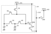
- FIG. 2 is a circuit diagram showing a configuration of a pixel according to the first embodiment.
- FIG. 3 is a schematic diagram showing how the solid-state imaging device according to the first embodiment resets the capacitance storage unit.
- FIG. 4 is a schematic diagram showing how the solid-state imaging device according to the first embodiment resets the floating diffusion portion.
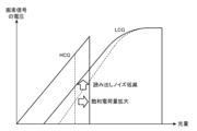
- FIG. 5 is a graph showing how the solid-state imaging device according to the first embodiment achieves both an increase in the amount of saturation charge and a reduction in readout noise when reading out charges stored in the capacitance storage section.
- FIG. 6 is a block diagram showing a configuration of a solid-state imaging device according to the second embodiment.
- FIG. 7 is a circuit diagram showing a configuration of a pixel according to the second embodiment.
- FIG. 8 is a schematic diagram showing how the solid-state imaging device according to the second embodiment resets the capacitance storage unit.
- FIG. 9 is a schematic diagram showing how the solid-state imaging device according to the second embodiment resets the floating diffusion portion.
- FIG. 10 is a block diagram showing a configuration of a solid-state imaging device according to the third embodiment.
- FIG. 11 is a circuit diagram showing a configuration of a pixel according to the third embodiment.
- FIG. 12 is a schematic diagram showing how the solid-state imaging device according to the third embodiment resets the capacitance storage unit.
- FIG. 13 is a schematic diagram showing how the solid-state imaging device according to the third embodiment resets the floating diffusion portion.
- FIG. 14 is a block diagram showing a configuration of a solid-state imaging device according to the fourth embodiment.
- FIG. 15 is a circuit diagram showing a configuration of a pixel according to the fourth embodiment.
- FIG. 16 is a schematic diagram showing how the solid-state imaging device according to the fourth embodiment transfers signal charges from the photoelectric conversion section to the second floating diffusion section.
- FIG. 17 is a schematic diagram showing how each transistor constituting a pixel according to the fourth embodiment is driven by each control signal output from the vertical scanning circuit according to the fourth embodiment.
- FIG. 18 is an example of a timing chart of each control signal when the vertical scanning circuit according to the fourth embodiment drives the pixel according to the fourth embodiment.
- FIG. 19 is a schematic diagram showing the potential of each component of a pixel according to the fourth embodiment.
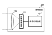
- FIG. 20 is a block diagram showing a configuration of an imaging device according to the fifth embodiment.
- the voltage applied to the gate of the transfer transistor must be kept within a certain voltage range (hereinafter referred to as the "reliability-ensuring voltage").
- the floating diffusion section and the capacitance storage section are configured to be reset with the same voltage.
- the inventors therefore conducted repeated experiments and studies in an effort to solve this problem. As a result, the inventors discovered that this problem could be solved if the voltage used to reset the floating diffusion section and the voltage used to reset the capacitance storage section could be made different from each other.
- a solid-state imaging device includes a pixel array in which a plurality of pixels are arranged in a matrix, and a first power supply wiring, each of the plurality of pixels includes a photoelectric conversion unit that converts received light into a signal charge, a floating diffusion unit for storing the signal charge, a capacitance storage unit for storing the signal charge, a first transfer transistor for reading the signal charge from the photoelectric conversion unit to the floating diffusion unit, an overflow transistor for discharging the signal charge overflowing from the photoelectric conversion unit to the capacitance storage unit, a second transfer transistor for transferring the signal charge stored in the capacitance storage unit to the floating diffusion unit, a first reset transistor having one of a source and a drain connected to one of the source and drain of the second transfer transistor and the other connected to the first power supply wiring, and an amplifying transistor having a gate connected to the floating diffusion unit, and the solid-state imaging device further includes reset means for resetting the floating diffusion unit and the capacitance storage unit with voltages
- the floating diffusion section and the capacitance storage section can be reset with different voltages.
- the solid-state imaging device having the above configuration, it is possible to achieve both a voltage for resetting the floating diffusion section that is higher than the reliability assurance voltage of the second transfer transistor and a voltage for resetting the capacitance storage section that is equal to or lower than the reliability assurance voltage of the second transfer transistor minus the threshold voltage of the second transfer transistor.
- the reset means may also include a second power supply wiring provided in the solid-state imaging device, and a second reset transistor provided in each of the plurality of pixels, one of a source and a drain connected to the one of the source and drain of the second transfer transistor and the other connected to the second power supply wiring.
- the first voltage of the first power supply wiring may be lower than the second voltage of the second power supply wiring.
- the voltage that resets the capacitance storage section may be the first voltage
- the voltage that resets the floating diffusion section may be the second voltage
- the reset means may also include a boost means provided in the solid-state imaging device for boosting the voltage of the floating diffusion section.
- the reset means may also include a voltage switching means for selectively switching the voltage of the first power supply wiring provided in the solid-state imaging device to either a first voltage or a second voltage different from the first voltage.
- the first voltage of the first power supply wiring may be lower than the second voltage.
- the voltage that resets the capacitance storage section may be the first voltage
- the voltage that resets the floating diffusion section may be the second voltage
- a solid-state imaging device is a solid-state imaging device including a pixel array in which a plurality of pixels are arranged in a matrix, and power supply wiring, and each of the plurality of pixels includes a photoelectric conversion unit that converts received light into a signal charge, a first floating diffusion unit for storing the signal charge, a second floating diffusion unit for storing the signal charge, a capacitance storage unit for storing the signal charge, a first transfer transistor for reading out the signal charge from the photoelectric conversion unit to the first floating diffusion unit, an overflow transistor for discharging the signal charge overflowing from the photoelectric conversion unit to the capacitance storage unit, a second transfer transistor for transferring the signal charge stored in the capacitance storage unit to the second floating diffusion unit, and a second transfer transistor having a source and a drain connected to the second transfer transistor.
- the solid-state imaging device further includes a vertical scanning circuit that, for each of the plurality of pixels, sets the fourth transfer transistor in a non-conductive state, sets the reset transistor in a non-conductive state, and sets the second transfer transistor in a conductive state.
- the signal charge that overflows from the second floating diffusion section through the non-conductive third transfer transistor can be stored in the capacitance storage section through the conductive second transfer transistor.
- An imaging device includes the above-described solid-state imaging device.
- the imaging device configured as described above can achieve both an increase in the amount of saturation charge and a reduction in readout noise when reading out the signal charge stored in the capacitance storage section, similar to the solid-state imaging device according to one aspect of the present disclosure.
- FIG. 1 is a block diagram showing a configuration of a solid-state imaging device 100 according to the first embodiment.
- the solid-state imaging device 100 includes a pixel array 11, a vertical scanning circuit 210, an AD conversion circuit 220, a control circuit 230, an HDR synthesis circuit 240, a first power supply 201, a second power supply 202, a first power supply wiring 101, and a second power supply wiring 102.
- the solid-state imaging device 100 is described here as having an HDR synthesis circuit 240, this is not necessarily limited to a configuration in which the solid-state imaging device 100 has an HDR synthesis circuit 240, and for example, the solid-state imaging device 100 may have an external device or the like that has an HDR synthesis circuit 240.
- the pixel array 11 is configured with a plurality of pixels 1 arranged in a matrix of m (m is an integer of 2 or more) rows and n (n is an integer of 2 or more) columns.
- the pixel array 11 further includes n vertical signal lines 110 extending in the column direction, each of which is connected to m pixels 1 arranged in the column direction, and m groups of control signal lines 120 extending in the row direction, each of which is connected to n pixels 1 arranged in the row direction.
- each of the n vertical signal lines 110 is a single signal line
- each of the m control signal line groups 120 is made up of multiple signal lines.
- n vertical signal lines 110 are described here as being each a single signal line, this is not necessarily limited to a configuration in which each of the n vertical signal lines 110 is a single signal line, and for example, there may be multiple vertical signal lines.
- the vertical scanning circuit 210 drives each pixel 1 of the pixel array 11 on a row-by-row basis via m groups of control signal lines 120.
- the AD conversion circuit 220 converts n analog pixel signals output from n pixels 1 on a row-by-row basis into n digital pixel signals via n vertical signal lines 110. The n digital pixel signals after AD conversion are then output to the HDR synthesis circuit 240.
- a correlated double sampling process is also performed to remove reset noise and the like during the read operation by calculating the difference between the result of AD conversion of the pixel signal read from pixel 1 in the reset state and the result of AD conversion of the pixel signal read from pixel 1 after exposure.
- the HDR synthesis circuit 240 generates an image by performing HDR synthesis on the pixel signals output from the AD conversion circuit 220.
- the first power supply 201 is a power supply that supplies a power supply voltage VDD1.
- the second power supply 202 is a power supply that supplies a power supply voltage VDD2.
- the power supply voltage VDD2 is described as being higher than the power supply voltage VDD1.
- the first power supply wiring 101 is a wiring for transmitting the power supply voltage VDD1 supplied from the first power supply 201 to the components inside the pixel array 11. For this reason, although not shown in FIG. 1, the first power supply wiring 101 is also present in the area overlapping the pixel array 11 in a plan view of the pixel array 11.
- the second power supply wiring 102 is a wiring for transmitting the power supply voltage VDD2 supplied from the second power supply 202 to the components inside the pixel array 11. For this reason, although not shown in FIG. 1, the second power supply wiring 102 also exists in the area overlapping the pixel array 11 in a plan view of the pixel array 11.
- Pixel 1 generates an electric charge according to the amount of light received, and outputs j pixel signals (j is an integer equal to or greater than 2) with different gains according to the amount of electric charge generated.
- j is described as 2. That is, in this embodiment, pixel 1 outputs two pixel signals: a low-gain pixel signal (hereinafter, the abbreviation “LCG (Low Conversion Gain)” may be used instead of the term “low gain”), and a high-gain pixel signal (hereinafter, the abbreviation “HCG (High Conversion Gain)” may be used instead of the term "high gain”), which is a pixel signal with a higher gain than the low-gain pixel signal.
- LCG Low Conversion Gain
- HCG High Conversion Gain
- FIG. 2 is a circuit diagram showing the configuration of pixel 1.
- pixel 1 includes a photoelectric conversion section 10, a floating diffusion section 20, a capacitance storage section 30, a first transfer transistor 40, an overflow transistor 50, a second transfer transistor 60, a first reset transistor 70, an amplification transistor 80, a selection transistor 90, and a second reset transistor 75.
- pixel 1 is described as having an overflow transistor 50, but as described below, overflow transistor 50 functions as a potential barrier between photoelectric conversion unit 10 and capacitance storage unit 30. Therefore, pixel 1 does not necessarily need to be limited to a configuration having an overflow transistor 50, as long as it is configured to have a component that functions as a potential barrier between photoelectric conversion unit 10 and capacitance storage unit 30 instead of overflow transistor 50.
- the photoelectric conversion unit 10 converts the received light into a signal charge. That is, the photoelectric conversion unit 10 generates a signal charge according to the amount of received light and accumulates the generated signal charge.
- the photoelectric conversion unit 10 is realized, for example, by a photodiode having a PN junction.
- the reception of light by the photoelectric conversion unit 10 is also referred to as exposure.
- the floating diffusion section 20 is a capacitance for storing the signal charge generated by the photoelectric conversion section 10.
- the floating diffusion section 20 changes the voltage by storing the signal charge. In other words, the floating diffusion section 20 converts the signal charge into a voltage signal.
- the capacitance storage unit 30 is a capacitance composed of a capacitor for storing the signal charge generated by the photoelectric conversion unit 10.
- the capacitance storage unit 30 is realized, for example, by a MIM (Metal Insulator Metal) capacitance.
- MIM Metal Insulator Metal
- One of the source and drain of the first transfer transistor 40 is connected to the photoelectric conversion section 10, and the other is connected to the floating diffusion section 20.
- the first transfer transistor 40 is an NMOS transistor, and its gate is driven by the vertical scanning circuit 210.
- the first transfer transistor 40 is non-conductive when its gate is at a logic low level, and is conductive when its gate is at a logic high level.
- the first transfer transistor 40 When the first transfer transistor 40 becomes conductive, the charge stored in the photoelectric conversion section 10 is transferred to the floating diffusion section 20 via the first transfer transistor 40.
- the first transfer transistor 40 functions as a transistor for reading out signal charges from the photoelectric conversion section 10 to the floating diffusion section 20.
- One of the source and drain of the overflow transistor 50 is connected to the photoelectric conversion unit 10, and the other is connected to the capacitance storage unit 30.
- the overflow transistor 50 is an NMOS transistor, and its gate is driven by the vertical scanning circuit 210.
- the gate of the overflow transistor 50 has been described here as being driven by the vertical scanning circuit 210, the gate of the overflow transistor 50 does not necessarily need to be limited to a configuration in which it is driven by the vertical scanning circuit 210.
- the gate of the overflow transistor 50 may be configured to be supplied with a constant voltage generated by a circuit block other than the vertical scanning circuit 210, for example.
- the overflow transistor 50 functions as a transistor for discharging the signal charge that has overflowed from the photoelectric conversion unit 10 to the capacitance storage unit 30.
- the second transfer transistor 60 has one of its source and drain connected to the capacitance storage section 30, and the other connected to the floating diffusion section 20.
- the second transfer transistor 60 is an NMOS transistor, and its gate is driven by the vertical scanning circuit 210.
- the second transfer transistor 60 is non-conductive when its gate is at a logic low level, and is conductive when its gate is at a logic high level.
- the second transfer transistor 60 When the second transfer transistor 60 is in a conductive state, the charge stored in the capacitance storage section 30 is transferred to the floating diffusion section 20 via the second transfer transistor 60, or the charge stored in the floating diffusion section 20 is transferred to the capacitance storage section 30 via the second transfer transistor 60.
- the second transfer transistor 60 functions as a transistor for transferring the signal charge stored in the capacitance storage section 30 to the floating diffusion section 20.
- the amplification transistor 80 has a gate connected to the floating diffusion section 20, a drain connected to the second power supply wiring 102, and a source connected to the drain of the selection transistor 90 (described later).
- the amplification transistor 80 is an NMOS transistor, and forms a source follower circuit together with a constant current source (not shown) arranged on the vertical signal line 110 connected via the selection transistor 90 (described later). As a result, when the selection transistor 90 (described later) is in a conductive state, the amplification transistor 80 outputs a pixel signal corresponding to the voltage of the floating diffusion section 20, i.e., the signal charge generated by the photoelectric conversion section 10, to the vertical signal line 110.
- the selection transistor 90 has a drain connected to the source of the amplification transistor 80 and a source connected to the vertical signal line 110.
- the selection transistor 90 is an NMOS transistor, and its gate is driven by the vertical scanning circuit 210.
- the gate of the selection transistor 90 When the gate of the selection transistor 90 is at a logic low level, it is non-conductive, and when the gate is at a logic high level, it is conductive.
- the selection transistor 90 When the selection transistor 90 is in a conductive state, the pixel signal output from the amplification transistor 80 is output to the vertical signal line 110 via the selection transistor 90. In other words, when the selection transistor 90 is in a conductive state, pixel 1 is in a selected state.
- the first reset transistor 70 has one of its source and drain connected to the other of the source and drain of the second transfer transistor 60, and the other connected to the first power supply wiring 101.
- the first reset transistor 70 is an NMOS transistor, and its gate is driven by the vertical scanning circuit 210.
- the first reset transistor 70 is non-conductive when its gate is at a logic low level, and is conductive when its gate is at a logic high level.
- the capacitance storage unit 30 is reset by the power supply voltage VDD1.
- the second reset transistor 75 has one of its source and drain connected to the other of the source and drain of the second transfer transistor 60, and the other connected to the second power supply wiring 102.
- the second reset transistor 75 is an NMOS transistor, and its gate is driven by the vertical scanning circuit 210.
- the second reset transistor 75 is non-conductive when its gate is at a logic low level, and is conductive when its gate is at a logic high level.
- the floating diffusion section 20 is reset by the power supply voltage VDD2.
- the vertical scanning circuit 210 drives each pixel 1 to reset the capacitance storage section 30 and the floating diffusion section 20 of each pixel 1 .
- FIG. 3 is a schematic diagram showing how the solid-state imaging device 100 resets the capacitance storage unit 30.
- the second transfer transistor 60 is in a conductive state, and the first transfer transistor 40, the overflow transistor 50, and the second reset transistor 75 are in a non-conductive state.
- the first reset transistor 70 is switched from a non-conductive state to a conductive state, thereby resetting the capacitance storage unit 30 with the power supply voltage VDD1.
- FIG. 4 is a schematic diagram showing how the solid-state imaging device 100 resets the floating diffusion section 20.
- the second reset transistor 75 is switched from a non-conductive state to a conductive state, thereby resetting the floating diffusion section 20 with the power supply voltage VDD2.
- the solid-state imaging device 100 having the above configuration is provided with a reset means including the second power supply wiring 102 and the second reset transistor 75 provided in each pixel 1, so that in each pixel 1, the floating diffusion section 20 and the capacitance storage section 30 can be reset with different voltages.
- the floating diffusion section 20 and the capacitance storage section 30 can be reset with different voltages.
- the solid-state imaging device 100 configured as described above can simultaneously reset the floating diffusion section 20 with a voltage higher than the reliability assurance voltage of the second transfer transistor 60 and reset the capacitance storage section 30 with a voltage equal to or lower than the reliability assurance voltage of the second transfer transistor 60 minus the threshold voltage of the second transfer transistor 60, while simultaneously increasing the amount of saturation charge and reducing readout noise when reading out the signal charge accumulated in the capacitance storage section 30.
- FIG. 5 is a graph showing how the solid-state imaging device 100 achieves both an increase in the amount of saturation charge and a reduction in read noise when reading out the charge stored in the capacitance storage section 30.
- the vertical axis represents the voltage of the pixel signal output from pixel 1
- the horizontal axis represents the amount of light received by the photoelectric conversion unit 10.
- the solid-state imaging device 100 when reading out a signal from the photoelectric conversion unit 10, the solid-state imaging device 100 resets the floating diffusion unit 20 at a high voltage, thereby increasing the amount of charge that can be read out, i.e., increasing the amount of saturated charge; and by resetting the signal charge accumulated in the capacitance storage unit 30 at a low voltage and increasing the gate voltage of the second transfer transistor 60, the accumulated signal charge can be completely discharged, eliminating residual signal charge (afterimage), thereby reducing noise during readout and improving the linearity of the signal.
- solid-state imaging device according to embodiment 2, components similar to those of solid-state imaging device 100 have already been explained, so the same reference numerals are used and detailed explanations are omitted, and the explanation focuses on the differences from solid-state imaging device 100.
- FIG. 6 is a block diagram showing a configuration of a solid-state imaging device 100A according to the second embodiment.
- the solid-state imaging device 100A is configured by adding n switches 200 to the solid-state imaging device 100 according to the first embodiment, changing the pixel array 11 to a pixel array 11A, and changing the vertical scanning circuit 210 to a vertical scanning circuit 210A.
- Each of the n switches 200 is connected to the second power supply wiring 102 and each of the n vertical signal lines 110, and is a switch that selectively switches the second power supply wiring 102 and the connected vertical signal line 110 between a conductive state and a non-conductive state.
- the power supply wiring to which the switch 200 is connected is described as the second power supply wiring 102, but the switch 200 may be configured so that the power supply wiring to which it is connected is connected to a power supply wiring other than the second power supply wiring 102.
- the switch 200 may be configured so that the power supply wiring to which it is connected is connected to a power supply wiring that is connected to a power supply that supplies a power supply voltage other than the power supply voltage VDD2.
- the vertical scanning circuit 210A is configured by changing the function of driving pixel 1 from the vertical scanning circuit 210 according to the first embodiment to a function of driving pixel 1A (described below), and further adding a function of driving n switches 200.
- the pixel array 11A is configured by replacing the multiple pixels 1 in the pixel array 11 according to the first embodiment with multiple pixels 1A.
- FIG. 7 is a circuit diagram showing the configuration of pixel 1A.
- pixel 1A is configured by deleting the second reset transistor 75 from pixel 1 according to embodiment 1 and changing the amplification transistor 80 to an amplification transistor 80A.
- the amplifier transistor 80A is configured by changing the drain connection destination from the amplifier transistor 80 according to the first embodiment from the second power supply wiring 102 to the first power supply wiring 101.
- the vertical scanning circuit 210A drives each pixel 1A and each switch 200, thereby resetting the capacitance storage section 30 and the floating diffusion section 20 of each pixel 1A.
- FIG. 8 is a schematic diagram showing how the solid-state imaging device 100A resets the capacitance storage unit 30.
- the second transfer transistor 60 is in a conductive state, and the overflow transistor 50 and the first transfer transistor 40 are in a non-conductive state.
- the first reset transistor 70 is switched from a non-conductive state to a conductive state, thereby resetting the capacitance storage unit 30 with the power supply voltage VDD1.
- the floating diffusion section 20 is reset by the power supply voltage VDD1 by making the second transfer transistor 60 and the first transfer transistor 40 non-conductive and switching the first reset transistor 70 from a non-conductive state to a conductive state.
- This state in which the floating diffusion section 20 is temporarily reset by the power supply voltage VDD1 is also referred to as a temporary reset state.
- FIG. 9 is a schematic diagram showing how the solid-state imaging device 100A resets the floating diffusion section 20.
- the solid-state imaging device 100A resets the floating diffusion portion 20 of the pixel 1A to be reset to a provisional reset state, and then resets the floating diffusion portion 20 to a voltage that is ⁇ higher than the power supply voltage VDD1 (i.e., VDD1+ ⁇ ) by boosting the vertical signal line 110 connected to the pixel 1A to be reset while the first transfer transistor 40, the second transfer transistor 60, the overflow transistor 50, and the first reset transistor 70 are in a non-conductive state.
- VDD1 power supply voltage
- the vertical scanning circuit 210A switches the switch 200 connected to the vertical signal line 110 connected to the pixel 1A to be reset from a non-conductive state to a conductive state, thereby boosting the vertical signal line 110 connected to the pixel 1A to be reset.
- the vertical signal line 110 connected to the pixel 1A to be reset and the floating diffusion section 20 of the pixel 1A to be reset have parasitic capacitance. Therefore, when the vertical signal line 110 connected to the pixel 1A to be reset is boosted, the floating diffusion section 20 of the pixel 1A to be reset is also boosted via this parasitic capacitance. In other words, if the voltage to which the floating diffusion section 20 is boosted is ⁇ , the voltage of the floating diffusion section 20 is VDD1 + ⁇ .
- the switch 200 functions as a boosting means for boosting the floating diffusion section 20 by ⁇ using the parasitic capacitance with the vertical signal line 110. For this reason, the switch 200 is also referred to as a boosting means 200.
- the floating diffusion section 20 is reset to the voltage VDD1+ ⁇ .
- the solid-state imaging device 100A having the above configuration is provided with a reset means including n boost means 200, so that in each pixel 1, the floating diffusion section 20 and the capacitance storage section 30 can be reset with different voltages.
- the number of switches 200 included in the solid-state imaging device 100A is described as n.
- the number of switches 200 included in the solid-state imaging device 100A does not necessarily need to be limited to the example configuration of n.
- the solid-state imaging device 100A may be configured to include, for example, one switch 200 capable of boosting each of the n vertical signal lines 110.
- the floating diffusion section 20 and the capacitance storage section 30 can be reset with different voltages.
- the solid-state imaging device 100A can achieve both an increase in the amount of saturation charge and a reduction in readout noise when reading out the charge stored in the capacitance storage section 30.
- solid-state imaging device according to embodiment 3, components similar to those of solid-state imaging device 100 have already been explained, so the same reference numerals are used and detailed explanations are omitted, and the explanation focuses on the differences from solid-state imaging device 100.
- FIG. 10 is a block diagram showing a configuration of a solid-state imaging device 100B according to the third embodiment.
- the solid-state imaging device 100B is configured by adding a switch 300 to the solid-state imaging device 100 according to embodiment 1, adding a third power supply wiring 103, changing the pixel array 11 to a pixel array 11B, changing the vertical scanning circuit 210 to a vertical scanning circuit 210B, changing the first power supply wiring 101 to a first power supply wiring 101B, and changing the second power supply wiring 102 to a second power supply wiring 102B.
- the third power supply wiring 103 is a wiring for transmitting the power supply voltage VDD1 supplied from the first power supply 201 to the switch 300.
- the second power supply wiring 102B is a wiring for transmitting the power supply voltage VDD2 supplied from the second power supply 202 to the switch 300.
- the switch 300 is a switch that alternatively switches between a state in which the third power supply wiring 103 and the first power supply wiring 101B are connected, and a state in which the second power supply wiring 102B and the first power supply wiring 101B are connected.
- the switch 300 is a switch that alternatively switches the voltage supplied to the first power supply wiring 101B to either the power supply voltage VDD1, which is the first voltage, or the power supply voltage VDD2, which is the second voltage.
- the switch 300 is also referred to as voltage switching means 300.
- the first power supply wiring 101B is a wiring for transmitting either the power supply voltage VDD1 or the power supply voltage VDD2, which is alternatively switched by the switch 300, to the components inside the pixel array 11B. For this reason, although not shown in FIG. 10, the first power supply wiring 101B also exists in the area overlapping the pixel array 11B in a plan view of the pixel array 11B.
- Vertical scanning circuit 210B is configured by changing the function of driving pixel 1 from vertical scanning circuit 210 according to embodiment 1 to a function of driving pixel 1B (described below), and further adding a function of driving switch 300.
- the pixel array 11B is configured by replacing the multiple pixels 1 in the pixel array 11 according to the first embodiment with multiple pixels 1B.
- FIG. 11 is a circuit diagram showing the configuration of pixel 1B.
- pixel 1B is configured by changing the first reset transistor 70 of pixel 1A according to embodiment 2 to a first reset transistor 70B, and changing the amplification transistor 80A to an amplification transistor 80B.
- the first reset transistor 70B is configured by changing the connection destination of the other of the source and drain from the first reset transistor 70 of embodiment 1 to the first power supply wiring 101B instead of the first power supply wiring 101.
- the amplifier transistor 80B is different from the amplifier transistor 80A according to the first embodiment in that the drain connection destination is changed from the first power supply wiring 101 to a power supply wiring other than the first power supply wiring 101B.
- the power supply wiring other than the first power supply wiring 101B may be, for example, the second power supply wiring 102B or the third power supply wiring 103.
- the vertical scanning circuit 210B drives each pixel 1B and the switch 300, thereby resetting the capacitance storage section 30 and the floating diffusion section 20 of each pixel 1B.
- FIG. 12 is a schematic diagram showing how the solid-state imaging device 100B resets the capacitance storage unit 30.
- the solid-state imaging device 100B has the switch 300 in a state in which the third power supply wiring 103 and the first power supply wiring 101B are connected, i.e., the voltage supplied to the first power supply wiring 101B is the power supply voltage VDD1, and for the pixel 1B to be reset, the second transfer transistor 60 is in a conductive state, and the first transfer transistor 40 and the overflow transistor 50 are in a non-conductive state.
- the first reset transistor 70B is switched from a non-conductive state to a conductive state, thereby resetting the capacitance storage unit 30 with the power supply voltage VDD1.
- FIG. 13 is a schematic diagram showing how the solid-state imaging device 100B resets the floating diffusion section 20.
- the solid-state imaging device 100B has the switch 300 in a state in which the second power supply wiring 102B and the first power supply wiring 101B are connected, i.e., the voltage supplied to the first power supply wiring 101B is the power supply voltage VDD2, and the first transfer transistor 40, the second transfer transistor 60, and the overflow transistor 50 are in a non-conductive state for the pixel 1B to be reset.
- the first reset transistor 70B is switched from a non-conductive state to a conductive state, thereby resetting the floating diffusion section 20 with the power supply voltage VDD2.
- the solid-state imaging device 100B having the above configuration is provided with a resetting means including a voltage switching means 300, so that in each pixel 1B, the floating diffusion section 20 and the capacitance storage section 30 can be reset with different voltages.
- the floating diffusion section 20 and the capacitance storage section 30 can be reset with different voltages.
- the solid-state imaging device 100B can achieve both an increase in the amount of saturated charge and a reduction in readout noise when reading out the charge stored in the capacitance storage unit 30.
- solid-state imaging device according to embodiment 4, components similar to those of solid-state imaging device 100 have already been explained, so the same reference numerals are used and detailed explanations are omitted, and the explanation focuses on the differences from solid-state imaging device 100.
- FIG. 14 is a block diagram showing a configuration of a solid-state imaging device 100C according to the fourth embodiment.
- the solid-state imaging device 100C is configured by deleting the second power supply 202 and the second power supply wiring 102 from the solid-state imaging device 100 according to embodiment 1, changing the pixel array 11 to a pixel array 11C, and changing the vertical scanning circuit 210 to a vertical scanning circuit 210C.
- Vertical scanning circuit 210C is configured by changing the function of driving pixel 1 from the vertical scanning circuit 210 according to embodiment 1 to a function of driving pixel 1C (described below).
- the pixel array 11C is configured by replacing the multiple pixels 1 in the pixel array 11 according to the first embodiment with multiple pixels 1C.
- pixel 1, pixel 1A, and pixel 1B are examples of configurations that output two pixel signals with different gains. In other words, they are examples of configurations where j is 2.
- pixel 1C is an example of a configuration that outputs three pixel signals with different gains. In other words, it is an example of a configuration where j is 3.
- pixel 1C is described as outputting three pixel signals: a low gain (LCG) pixel signal, a high gain (HCG) pixel signal, and a medium gain pixel signal that has a higher gain than the low gain pixel signal and a lower gain than the high gain pixel signal (hereinafter, the abbreviation "MCG (Medium Conversion Gain)” may be used instead of the term “medium gain”).
- LCG low gain
- HCG high gain
- MCG Medium Conversion Gain
- FIG. 15 is a circuit diagram showing the configuration of pixel 1C.
- pixel 1C is configured by deleting the second reset transistor 75 from pixel 1 according to embodiment 1, changing the floating diffusion section 20 to a first floating diffusion section 21, changing the amplification transistor 80 to an amplification transistor 80A, and adding a second floating diffusion section 22, a third transfer transistor 43, and a fourth transfer transistor 44.
- connection destination of the other of the source and drain of the first transfer transistor 40 is changed from the floating diffusion section 20 to the first floating diffusion section 21.
- the second floating diffusion section 22 is a capacitance for storing the signal charge generated by the photoelectric conversion section 10.
- the third transfer transistor 43 has one of its source and drain connected to the first floating diffusion section 21, and the other connected to the second floating diffusion section 22.
- the third transfer transistor 43 is an NMOS transistor, and its gate is driven by the vertical scanning circuit 210C.
- the third transfer transistor 43 is non-conductive when its gate is at a logic low level, and is conductive when its gate is at a logic high level.
- the third transfer transistor 43 becomes conductive, the charge stored in the first floating diffusion section 21 is transferred to the second floating diffusion section 22 via the third transfer transistor 43, or the charge stored in the second floating diffusion section 22 is transferred to the first floating diffusion section 21 via the third transfer transistor 43.
- the fourth transfer transistor 44 has one of its source and drain connected to the second floating diffusion section 22, and the other connected to the other of the source and drain of the first reset transistor 70.
- the fourth transfer transistor 44 is an NMOS transistor, and its gate is driven by the vertical scanning circuit 210C.
- the fourth transfer transistor 44 is non-conductive when its gate is at a logic low level, and is conductive when its gate is at a logic high level.
- the fourth transfer transistor 44 becomes conductive, the charge stored in the second floating diffusion section 22 is transferred to one of the source and drain of the first reset transistor 70 via the fourth transfer transistor 44, or the charge stored in one of the source and drain of the first reset transistor 70 is transferred to the second floating diffusion section 22 via the fourth transfer transistor 44.
- the first transfer transistor 40 functions as a transistor for reading out signal charge from the photoelectric conversion section 10 to the first floating diffusion section 21
- the second transfer transistor 60 functions as a transistor for transferring signal charge stored in the capacitance storage section 30 to the second floating diffusion section 22.
- the vertical scanning circuit 210C drives each pixel 1C, so that a signal charge is transferred from the photoelectric conversion unit 10 of each pixel 1C to the first floating diffusion unit 21 and the second floating diffusion unit 22. Transfer.
- FIG. 16 is a schematic diagram showing how the solid-state imaging device 100C transfers signal charges from the photoelectric conversion section 10 to the first floating diffusion section 21 and the second floating diffusion section 22.
- the solid-state imaging device 100C transfers signal charge from the photoelectric conversion unit 10 to the first floating diffusion unit 21 and the second floating diffusion unit 22 by making the first transfer transistor 40, the second transfer transistor 60, and the third transfer transistor 43 conductive and making the first reset transistor 70, the overflow transistor 50, and the fourth transfer transistor 44 non-conductive.
- the signal charge is transferred from the photoelectric conversion unit 10 to the first floating diffusion unit 21 and the second floating diffusion unit 22 if the signal charge generated by the photoelectric conversion unit 10 exceeds a certain amount, the signal charge that cannot be stored in the first floating diffusion unit 21 and the second floating diffusion unit 22 may exceed the potential barrier of the non-conducting fourth transfer transistor 44 and overflow to the first reset transistor 70 side.
- the overflowing signal charge is stored in the capacitance storage section 30 without flowing to the first power supply wiring 101.
- FIG. 17 is a schematic diagram showing how each transistor constituting a pixel 1C is driven by each control signal output from a vertical scanning circuit 210C.
- the first transfer transistor 40 is driven by a control signal TG
- the overflow transistor 50 is driven by a control signal OF
- the second transfer transistor 60 is driven by a control signal TGC
- the first reset transistor 70 is driven by a control signal RS
- the third transfer transistor 43 is driven by a control signal GC1
- the fourth transfer transistor 44 is driven by a control signal GC2
- the selection transistor 90 is driven by SEL.
- FIG. 18 is an example of a timing chart of each control signal when driving one or more pixels 1C during one horizontal scanning period, which is a selection period during which the vertical scanning circuit 210C selects one or more pixels 1C arranged in one row of the pixel array 11C.
- the horizontal axis represents time
- the vertical axis represents the logical value of each control signal.
- the vertical scanning circuit 210C first sets the control signal GC2 to a logic low level at time t14 to put the fourth transfer transistor 44 in a non-conductive state, then sets the control signal RS to a logic low level at time t15 to put the first reset transistor 70 in a non-conductive state, and then sets the control signal TGC to a logic high level at time t16 to put the second transfer transistor 60 in a conductive state. Then, thereafter, for the period from time t19 to t20, the control signal TG is set to a logic high level to put the first transfer transistor 40 in a conductive state.
- the charge signal of the photoelectric conversion unit 10 is transferred to the first floating diffusion unit 21. Then, during the period from time t20 to t21, the HCG pixel signal corresponding to the signal charge transferred to the first floating diffusion unit 21 is read out from the vertical signal line 110.
- control signal TG and the control signal GC1 are set to a logic high level, and the first transfer transistor 40 and the third transfer transistor 43 are placed in a conductive state.
- the charge signals of the photoelectric conversion section 10 and the first floating diffusion section 21 are distributed to the first floating diffusion section 21 and the second floating diffusion section 22. Then, during the period from time t22 to t23, the MCG pixel signals corresponding to the signal charges distributed to the first floating diffusion section 21 and the second floating diffusion section 22 are read out from the vertical signal line 110.
- FIG. 19 is a schematic diagram showing the potentials of the photoelectric conversion section 10 (PD in FIG. 19), the first floating diffusion section 21 (FD0 in FIG. 19), the second floating diffusion section 22 (FD1 in FIG. 19), one of the source and drain of the first reset transistor 70 (FD3 in FIG. 19), and the capacitance storage section 30 (FD2 in FIG. 19) during the period from time t21 to t22 in FIG. 18.
- Paths A, B, C, and D in FIG. 19 correspond to paths A, B, C, and D in FIG. 17, respectively.
- path C a potential barrier of the first reset transistor 70 in a non-conductive state exists between one of the source and drain of the first reset transistor 70 (FD3) and the first power supply wiring 101 (VDD1).
- path D no potential barrier exists between one of the source and drain of the first reset transistor 70 (FD3) and the capacitance storage unit 30 (FD2).
- the signal charge that has overflowed from the second floating diffusion section 22 to the first reset transistor 70 side, overcoming the potential barrier of the non-conductive fourth transfer transistor 44, is stored in the capacitance storage section 30 without flowing out to the first power supply wiring 101 by overflowing the potential barrier of the non-conductive first reset transistor 70 on path C.
- control signals during the period from time t19 to t20 and the control signals during the period from time t21 to t22 are similar except that the control signal GC1 is at a logic low level during the period from time t19 to t20 and at a logic high level during the period from time t19 to t20.
- the state in which the control signal GC1 is at a logical low level as indicated by the dashed line indicates the potential of the photoelectric conversion unit 10, the first floating diffusion unit 21, the second floating diffusion unit 22, one of the source and drain of the first reset transistor 70, and the capacitance storage unit 30 during the period from time t21 to t22 in FIG. 18.
- the signal charge that has overflowed from the first floating diffusion section 21 to the second floating diffusion section 22 by exceeding the potential barrier of the non-conductive third transfer transistor 43, and further overflowed from the second floating diffusion section 22 to the first reset transistor 70 by exceeding the potential barrier of the non-conductive fourth transfer transistor 44, is stored in the capacitance storage section 30 without flowing to the first power supply wiring 101, as in the case of the period from time t21 to t22.
- the vertical scanning circuit 210C sets the fourth transfer transistor 44 to a non-conductive state, the first reset transistor 70 to a non-conductive state, and the second transfer transistor 60 to a conductive state for each pixel 1C on a row-by-row basis in the pixel array 11. This makes it possible to prevent the signal charge generated by the photoelectric conversion unit 10 from flowing out of the pixel 1C even if the saturation charge amount of the photoelectric conversion unit 10 is increased, thereby improving the linearity of the signal.
- the vertical scanning circuit 210C sets the fourth transfer transistor 44 to a non-conductive state, the first reset transistor 70 to a non-conductive state, and the second transfer transistor 60 to a conductive state for each pixel 1C in row units in the pixel array 11, thereby allowing the signal charge overflowing from the first floating diffusion portion 21 and the second floating diffusion portion 22 to be stored in the capacitance storage portion 30.
- the solid-state imaging device 100C configured as described above can achieve both an increase in the amount of saturation charge and a reduction in readout noise when reading out the signal charge stored in the capacitance storage section 30.
- the pixel 1C has been described as having a configuration in which the second reset transistor 75 has been removed from the pixel 1 according to the first embodiment, but the pixel 1C does not necessarily need to be limited to a configuration in which the second reset transistor 75 has been removed from the pixel 1.
- the pixel 1C may have a configuration in which the floating diffusion section 20 of the pixel 1 according to the first embodiment is changed to a first floating diffusion section 21, and a second floating diffusion section 22, a third transfer transistor 43, and a fourth transfer transistor 44 are added.
- the solid-state imaging device 100C has been described as an example of a configuration in which, compared to pixel 1 of the solid-state imaging device 100 of embodiment 1, the second reset transistor 75 has been deleted, the floating diffusion section 20 has been changed to a first floating diffusion section 21, the amplifying transistor 80 has been changed to an amplifying transistor 80A, and a second floating diffusion section 22, a third transfer transistor 43, and a fourth transfer transistor 44 have been added.
- the solid-state imaging device 100C is not necessarily limited to the above configuration.
- the solid-state imaging device 100C may be configured, for example, by modifying pixel 1A of solid-state imaging device 100A according to embodiment 2 such that floating diffusion section 20 is changed to a first floating diffusion section 21 and a second floating diffusion section 22, a third transfer transistor 43, and a fourth transfer transistor 44 are added; or, for example, by modifying pixel 1B of solid-state imaging device 100B according to embodiment 3 such that floating diffusion section 20 is changed to a first floating diffusion section 21 and a second floating diffusion section 22, a third transfer transistor 43, and a fourth transfer transistor 44 are added.
- the imaging device according to embodiment 5 will be described as including the solid-state imaging device 100 according to embodiment 1, but the imaging device according to embodiment 5 does not necessarily need to be limited to a configuration including the solid-state imaging device 100 according to embodiment 1 as long as it includes the solid-state imaging device according to any one of embodiments 1 to 4.
- FIG. 20 is a block diagram showing a configuration of an imaging device 400 according to the fifth embodiment.
- the imaging device 400 is, for example, a digital still camera, a handheld video recorder, etc.
- the imaging device 400 includes a solid-state imaging device 100, a signal processing device 410, and a lens 420.
- the lens 420 focuses light from the subject that is the object of imaging by the imaging device 400 onto the area in the solid-state imaging device 100 where the pixel array 11 is formed, and forms an image of the subject onto the area in the solid-state imaging device 100 where the pixel array 11 is formed.
- the signal processing device 410 performs various signal processing on the signal (e.g., image) output from the solid-state imaging device 100.
- solid-state imaging device 100, solid-state imaging device 100A, solid-state imaging device 100B, and solid-state imaging device 100C can achieve both an increase in the amount of saturated charge and a reduction in readout noise when reading out signal charge stored in capacitance storage section 30.
- the imaging device 400 configured as described above, it is possible to achieve both an increase in the amount of saturation charge and a reduction in read noise when reading out the signal charge stored in the capacitance storage section 30, thereby achieving a wider HDR.
- This disclosure can be widely used in solid-state imaging devices that capture images.
Landscapes
- Engineering & Computer Science (AREA)
- Multimedia (AREA)
- Signal Processing (AREA)
- Solid State Image Pick-Up Elements (AREA)
- Transforming Light Signals Into Electric Signals (AREA)
Priority Applications (3)
| Application Number | Priority Date | Filing Date | Title |
|---|---|---|---|
| JP2024574868A JPWO2024162220A1 (https=) | 2023-01-31 | 2024-01-26 | |
| CN202480009574.7A CN120615336A (zh) | 2023-01-31 | 2024-01-26 | 固体摄像装置以及摄像装置 |
| US19/273,625 US20250344000A1 (en) | 2023-01-31 | 2025-07-18 | Solid-state imaging device and imaging apparatus |
Applications Claiming Priority (4)
| Application Number | Priority Date | Filing Date | Title |
|---|---|---|---|
| US202363442311P | 2023-01-31 | 2023-01-31 | |
| US202363442317P | 2023-01-31 | 2023-01-31 | |
| US63/442,317 | 2023-01-31 | ||
| US63/442,311 | 2023-01-31 |
Related Child Applications (1)
| Application Number | Title | Priority Date | Filing Date |
|---|---|---|---|
| US19/273,625 Continuation US20250344000A1 (en) | 2023-01-31 | 2025-07-18 | Solid-state imaging device and imaging apparatus |
Publications (1)
| Publication Number | Publication Date |
|---|---|
| WO2024162220A1 true WO2024162220A1 (ja) | 2024-08-08 |
Family
ID=92146748
Family Applications (2)
| Application Number | Title | Priority Date | Filing Date |
|---|---|---|---|
| PCT/JP2024/002491 Ceased WO2024162220A1 (ja) | 2023-01-31 | 2024-01-26 | 固体撮像装置および撮像装置 |
| PCT/JP2024/002494 Ceased WO2024162221A1 (ja) | 2023-01-31 | 2024-01-26 | 固体撮像装置および撮像装置 |
Family Applications After (1)
| Application Number | Title | Priority Date | Filing Date |
|---|---|---|---|
| PCT/JP2024/002494 Ceased WO2024162221A1 (ja) | 2023-01-31 | 2024-01-26 | 固体撮像装置および撮像装置 |
Country Status (4)
| Country | Link |
|---|---|
| US (2) | US20250350857A1 (https=) |
| JP (2) | JPWO2024162221A1 (https=) |
| CN (2) | CN120604523A (https=) |
| WO (2) | WO2024162220A1 (https=) |
Citations (7)
| Publication number | Priority date | Publication date | Assignee | Title |
|---|---|---|---|---|
| JPH02272742A (ja) * | 1989-04-14 | 1990-11-07 | Toshiba Corp | 電荷転送装置 |
| CN105791715A (zh) * | 2016-03-10 | 2016-07-20 | 长春长光辰芯光电技术有限公司 | 高动态范围图像传感器像素的全局快门控制方法 |
| US20200154066A1 (en) * | 2018-11-09 | 2020-05-14 | Semiconductor Components Industries, Llc | Image sensors having high dynamic range imaging pixels |
| US20210029312A1 (en) * | 2019-07-22 | 2021-01-28 | Semiconductor Components Industries, Llc | Imaging systems and methods for generating high dynamic range images |
| WO2021106402A1 (ja) * | 2019-11-29 | 2021-06-03 | ソニーセミコンダクタソリューションズ株式会社 | 半導体装置、撮像素子、及び電子機器 |
| WO2021166584A1 (ja) * | 2020-02-18 | 2021-08-26 | ヌヴォトンテクノロジージャパン株式会社 | 固体撮像装置、及びそれを用いる撮像装置 |
| WO2021235101A1 (ja) * | 2020-05-20 | 2021-11-25 | ソニーセミコンダクタソリューションズ株式会社 | 固体撮像装置 |
Family Cites Families (3)
| Publication number | Priority date | Publication date | Assignee | Title |
|---|---|---|---|---|
| JP5419659B2 (ja) * | 2009-12-04 | 2014-02-19 | キヤノン株式会社 | 撮像装置 |
| JP2013090127A (ja) * | 2011-10-18 | 2013-05-13 | Olympus Corp | 固体撮像装置および撮像装置 |
| CN117441346A (zh) * | 2021-06-09 | 2024-01-23 | 新唐科技日本株式会社 | 固体摄像装置、摄像装置及测距摄像装置 |
-
2024
- 2024-01-26 CN CN202480009573.2A patent/CN120604523A/zh active Pending
- 2024-01-26 JP JP2024574869A patent/JPWO2024162221A1/ja active Pending
- 2024-01-26 JP JP2024574868A patent/JPWO2024162220A1/ja active Pending
- 2024-01-26 WO PCT/JP2024/002491 patent/WO2024162220A1/ja not_active Ceased
- 2024-01-26 CN CN202480009574.7A patent/CN120615336A/zh active Pending
- 2024-01-26 WO PCT/JP2024/002494 patent/WO2024162221A1/ja not_active Ceased
-
2025
- 2025-07-16 US US19/271,041 patent/US20250350857A1/en active Pending
- 2025-07-18 US US19/273,625 patent/US20250344000A1/en active Pending
Patent Citations (7)
| Publication number | Priority date | Publication date | Assignee | Title |
|---|---|---|---|---|
| JPH02272742A (ja) * | 1989-04-14 | 1990-11-07 | Toshiba Corp | 電荷転送装置 |
| CN105791715A (zh) * | 2016-03-10 | 2016-07-20 | 长春长光辰芯光电技术有限公司 | 高动态范围图像传感器像素的全局快门控制方法 |
| US20200154066A1 (en) * | 2018-11-09 | 2020-05-14 | Semiconductor Components Industries, Llc | Image sensors having high dynamic range imaging pixels |
| US20210029312A1 (en) * | 2019-07-22 | 2021-01-28 | Semiconductor Components Industries, Llc | Imaging systems and methods for generating high dynamic range images |
| WO2021106402A1 (ja) * | 2019-11-29 | 2021-06-03 | ソニーセミコンダクタソリューションズ株式会社 | 半導体装置、撮像素子、及び電子機器 |
| WO2021166584A1 (ja) * | 2020-02-18 | 2021-08-26 | ヌヴォトンテクノロジージャパン株式会社 | 固体撮像装置、及びそれを用いる撮像装置 |
| WO2021235101A1 (ja) * | 2020-05-20 | 2021-11-25 | ソニーセミコンダクタソリューションズ株式会社 | 固体撮像装置 |
Also Published As
| Publication number | Publication date |
|---|---|
| JPWO2024162221A1 (https=) | 2024-08-08 |
| WO2024162221A1 (ja) | 2024-08-08 |
| US20250350857A1 (en) | 2025-11-13 |
| CN120604523A (zh) | 2025-09-05 |
| JPWO2024162220A1 (https=) | 2024-08-08 |
| US20250344000A1 (en) | 2025-11-06 |
| CN120615336A (zh) | 2025-09-09 |
Similar Documents
| Publication | Publication Date | Title |
|---|---|---|
| US10694121B2 (en) | Solid-state imaging device, method for driving solid-state imaging device, and electronic apparatus | |
| US11146752B2 (en) | Solid-state imaging apparatus, driving method of the solid-state imaging apparatus, and electronic equipment | |
| US9961262B2 (en) | Solid-state imaging device having a switchable conversion gain in the floating diffusion, method for driving solid-state imaging device, and electronic apparatus | |
| US9338381B2 (en) | Solid-state image-pickup device, image-pickup device, and signal reading method | |
| US8289425B2 (en) | Solid-state image pickup device with an improved output amplifier circuitry | |
| EP2180514B1 (en) | Solid state image sensor, method for driving a solid state image sensor and imaging apparatus | |
| CN202395873U (zh) | 固体摄像器件和电子装置 | |
| US9426402B2 (en) | Solid-state image pickup device, image pickup device, and signal reading method | |
| JP2020113892A (ja) | 固体撮像装置、固体撮像装置の駆動方法、および電子機器 | |
| US8830368B2 (en) | Solid-state imaging device | |
| US20100238332A1 (en) | Solid-state imaging device, driving method thereof, and electronic apparatus | |
| JP5535685B2 (ja) | 固体撮像装置及び駆動方法 | |
| JP6037178B2 (ja) | 固体撮像装置及び撮像装置 | |
| US9172893B2 (en) | Solid-state imaging device and imaging apparatus | |
| US8823069B2 (en) | Solid-state imaging device, drive method of solid-state imaging device, and imaging apparatus | |
| US20200068147A1 (en) | Imaging device, imaging system, and movable object | |
| TWI814893B (zh) | 固態攝像裝置及電子機器 | |
| US7550704B2 (en) | Solid state imaging device, method of driving solid state imaging device, and image pickup apparatus | |
| WO2012053127A1 (ja) | 固体撮像装置、その駆動方法及び撮像装置 | |
| WO2024162220A1 (ja) | 固体撮像装置および撮像装置 |
Legal Events
| Date | Code | Title | Description |
|---|---|---|---|
| 121 | Ep: the epo has been informed by wipo that ep was designated in this application |
Ref document number: 24750169 Country of ref document: EP Kind code of ref document: A1 |
|
| ENP | Entry into the national phase |
Ref document number: 2024574868 Country of ref document: JP Kind code of ref document: A |
|
| WWE | Wipo information: entry into national phase |
Ref document number: 2024574868 Country of ref document: JP |
|
| WWE | Wipo information: entry into national phase |
Ref document number: 202480009574.7 Country of ref document: CN |
|
| NENP | Non-entry into the national phase |
Ref country code: DE |
|
| WWP | Wipo information: published in national office |
Ref document number: 202480009574.7 Country of ref document: CN |
|
| 122 | Ep: pct application non-entry in european phase |
Ref document number: 24750169 Country of ref document: EP Kind code of ref document: A1 |