WO2024161996A1 - 半導体装置 - Google Patents
半導体装置 Download PDFInfo
- Publication number
- WO2024161996A1 WO2024161996A1 PCT/JP2024/001083 JP2024001083W WO2024161996A1 WO 2024161996 A1 WO2024161996 A1 WO 2024161996A1 JP 2024001083 W JP2024001083 W JP 2024001083W WO 2024161996 A1 WO2024161996 A1 WO 2024161996A1
- Authority
- WO
- WIPO (PCT)
- Prior art keywords
- semiconductor device
- thickness direction
- support member
- conductive support
- mounting portion
- Prior art date
- Legal status (The legal status is an assumption and is not a legal conclusion. Google has not performed a legal analysis and makes no representation as to the accuracy of the status listed.)
- Ceased
Links
Images


Classifications
-
- H—ELECTRICITY
- H05—ELECTRIC TECHNIQUES NOT OTHERWISE PROVIDED FOR
- H05K—PRINTED CIRCUITS; CASINGS OR CONSTRUCTIONAL DETAILS OF ELECTRIC APPARATUS; MANUFACTURE OF ASSEMBLAGES OF ELECTRICAL COMPONENTS
- H05K1/00—Printed circuits
- H05K1/02—Details
-
- H—ELECTRICITY
- H10—SEMICONDUCTOR DEVICES; ELECTRIC SOLID-STATE DEVICES NOT OTHERWISE PROVIDED FOR
- H10W—GENERIC PACKAGES, INTERCONNECTIONS, CONNECTORS OR OTHER CONSTRUCTIONAL DETAILS OF DEVICES COVERED BY CLASS H10
- H10W72/00—Interconnections or connectors in packages
-
- H—ELECTRICITY
- H10—SEMICONDUCTOR DEVICES; ELECTRIC SOLID-STATE DEVICES NOT OTHERWISE PROVIDED FOR
- H10W—GENERIC PACKAGES, INTERCONNECTIONS, CONNECTORS OR OTHER CONSTRUCTIONAL DETAILS OF DEVICES COVERED BY CLASS H10
- H10W90/00—Package configurations
Definitions
- This disclosure relates to a semiconductor device.
- An object of the present disclosure is to provide a semiconductor device that is an improvement over conventional semiconductor devices.
- an object of the present disclosure is to provide a semiconductor device that is suitable for simplifying the structure and reducing manufacturing costs.
- the semiconductor device provided by the first aspect of the present disclosure comprises a conductive support member, a first semiconductor element arranged on one side of the conductive support member in the thickness direction, and a first mounting portion and a second mounting portion spaced apart from each other in a direction perpendicular to the thickness direction.
- the first semiconductor element has a first element main surface facing one side in the thickness direction, and a first element back surface facing the other side in the thickness direction.
- the first mounting portion is arranged on the first element main surface and is conductive to the conductive support member.
- the second mounting portion is arranged on one side of the conductive support member in the thickness direction, and is conductive to the conductive support member.
- the above configuration simplifies the structure of the semiconductor device and reduces manufacturing costs.
- FIG. 1 is a plan view showing a semiconductor device according to a first embodiment of the present disclosure.
- FIG. 2 is a right side view showing the semiconductor device according to the first embodiment of the present disclosure.
- FIG. 3 is a bottom view showing the semiconductor device according to the first embodiment of the present disclosure.
- FIG. 4 is a cross-sectional view taken along line IV-IV in FIG.
- FIG. 5 is a plan view showing a semiconductor device according to the second embodiment of the present disclosure.
- FIG. 6 is a right side view showing a semiconductor device according to a second embodiment of the present disclosure.
- FIG. 7 is a bottom view showing a semiconductor device according to a second embodiment of the present disclosure.
- FIG. 8 is a cross-sectional view taken along line VIII-VIII in FIG. FIG.
- FIG. 9 is a cross-sectional view showing a semiconductor device according to a first modification of the second embodiment.
- FIG. 10 is a plan view showing a semiconductor device according to a third embodiment of the present disclosure.
- FIG. 11 is a right side view showing a semiconductor device according to a third embodiment of the present disclosure.
- FIG. 12 is a bottom view showing a semiconductor device according to a third embodiment of the present disclosure.
- FIG. 13 is a cross-sectional view taken along line XIII-XIII in FIG.
- FIG. 14 is a plan view showing a semiconductor device according to a fourth embodiment of the present disclosure.
- FIG. 15 is a right side view showing a semiconductor device according to a fourth embodiment of the present disclosure.
- FIG. 16 is a bottom view showing a semiconductor device according to a fourth embodiment of the present disclosure.
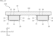
- FIG. 17 is a cross-sectional view taken along line XVII-XVII in FIG.
- FIG. 18 is a right side view showing a semiconductor device according to a first modification of the fourth embodiment.
- FIG. 19 is a bottom view showing a semiconductor device according to a first modification of the fourth embodiment.
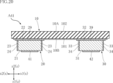
- FIG. 20 is a cross-sectional view showing a semiconductor device according to a first modification of the fourth embodiment.
- FIG. 21 is a plan view showing a semiconductor device according to a second modification of the fourth embodiment.
- FIG. 22 is a right side view showing a semiconductor device according to a second modification of the fourth embodiment.
- FIG. 17 is a cross-sectional view taken along line XVII-XVII in FIG.
- FIG. 18 is a right side view showing a semiconductor device according to a first modification of the fourth embodiment.
- FIG. 19 is a bottom view showing a semiconductor
- FIG. 23 is a bottom view showing a semiconductor device according to a second modification of the fourth embodiment.
- FIG. 24 is a right side view showing a semiconductor device according to a fifth embodiment of the present disclosure.
- FIG. 25 is a diagram showing a state in which the semiconductor device according to the fifth embodiment of the present disclosure is in use.
- FIG. 26 is a plan view showing a semiconductor device according to the sixth embodiment of the present disclosure.
- FIG. 27 is a right side view showing a semiconductor device according to a sixth embodiment of the present disclosure.
- FIG. 28 is a bottom view showing a semiconductor device according to a sixth embodiment of the present disclosure.
- FIG. 29 is a cross-sectional view taken along line XXIX-XXIX in FIG.
- an object A is formed on an object B" and “an object A is formed on an object B” include “an object A is formed directly on an object B” and “an object A is formed on an object B with another object interposed between the object A and the object B” unless otherwise specified.
- an object A is disposed on an object B” and “an object A is disposed on an object B” include “an object A is disposed directly on an object B” and “an object A is disposed on an object B with another object interposed between the object A and the object B" unless otherwise specified.
- an object A is located on an object B includes “an object A is located on an object B in contact with an object B” and “an object A is located on an object B with another object interposed between the object A and the object B” unless otherwise specified.
- an object A overlaps an object B when viewed in a certain direction includes “an object A overlaps the entire object B” and “an object A overlaps a part of an object B.”
- a surface A faces in direction B is not limited to the case where the angle of surface A with respect to direction B is 90°, but also includes the case where surface A is tilted with respect to direction B.
- the semiconductor device A10 of this embodiment includes a conductive support member 10, a first semiconductor element 20, a first mounting portion 41, and a second mounting portion 42.
- the semiconductor device A10 further includes a conductive bonding layer 29.
- the semiconductor device A10 does not include a sealing resin, and each of the elements constituting the semiconductor device A10 (the conductive support member 10, the first semiconductor element 20, the first mounting portion 41, and the second mounting portion 42) is exposed to the outside.
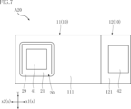
- FIG. 1 is a plan view of semiconductor device A10.
- FIG. 2 is a right side view of semiconductor device A10.
- FIG. 3 is a bottom view of semiconductor device A10.
- FIG. 4 is a cross-sectional view taken along line IV-IV in FIG. 1.
- the semiconductor device A10 shown in these figures is a device that is surface-mounted on the circuit boards of various devices.
- three mutually orthogonal directions will be referred to as appropriate.
- the thickness direction of the conductive support member 10 is an example of a "thickness direction” and is referred to as the "thickness direction z".
- One direction that is orthogonal to the thickness direction z (the left-right direction in Figures 1 to 4) is referred to as the "first direction x”.
- a direction that is orthogonal to both the thickness direction z and the first direction x (the up-down direction in Figure 1) is referred to as the "second direction y".
- the semiconductor device A10 is an elongated rectangle when viewed in the thickness direction z (in a plan view).
- the conductive support member 10 supports the first semiconductor element 20.
- the conductive support member 10 is made of a metal plate material.
- the constituent material of the conductive support member 10 is, for example, copper (Cu) or a copper alloy.
- the conductive support member 10 is, for example, a metal plate material that has been punched or bent.
- the conductive support member 10 includes a first portion 11, a second portion 12, and a third portion 13. As shown in Figures 2 and 4, the first portion 11, the second portion 12, and the third portion 13 are appropriately bent and connected when viewed in the second direction y.
- the first portion 11 has a first main surface 111 and a first back surface 112.
- the first main surface 111 faces the z1 side in the thickness direction z and faces the first semiconductor element 20.
- the first semiconductor element 20 is supported on the first main surface 111 via a conductive bonding layer 29 described below.
- the first back surface 112 faces the z2 side in the thickness direction z.
- the second part 12 is located on the z1 side of the first part 11 in the thickness direction z.
- the second part 12 has a second main surface 121 and a second back surface 122.
- the second main surface 121 faces the z1 side of the thickness direction z.
- the second back surface 122 faces the z2 side of the thickness direction z.
- the second main surface 121 is located on the z1 side of the thickness direction z relative to the first main surface 111 of the first part 11 in the thickness direction z.
- the third portion 13 is connected to the end of the first portion 11 on the x1 side in the first direction x.
- the third portion 13 is connected to the end of the second portion 12 on the x2 side in the first direction x.
- the first portion 11 and the second portion 12 do not overlap in the thickness direction z.
- the first portion 11, the second portion 12, and the third portion 13 are bent in a so-called step-like shape.
- the surfaces of each portion of the conductive support member 10 may be plated with tin (Sn), for example.
- tin plating multiple metal platings may be used, for example, layered in the order of nickel (Ni), palladium (Pd), and gold (Au).
- the first semiconductor element 20 is an element that performs the electrical function of the semiconductor device A10. There is no particular limitation on the type of the first semiconductor element 20. In this embodiment, the first semiconductor element 20 is a diode. In this embodiment, the first semiconductor element 20 is rectangular when viewed in the thickness direction z.
- the first semiconductor element 20 has a first element main surface 21, a first element back surface 22, a plurality of first element side surfaces 23, and an insulating layer 24.
- the first element main surface 21 and the first element back surface 22 face opposite each other in the thickness direction z.
- the first element main surface 21 faces the z1 side in the thickness direction z.
- the first element back surface 22 faces the z2 side in the thickness direction z.
- an electrode is formed on each of the first element main surface 21 and the first element back surface 22.
- the electrode formed on the first element main surface 21 is an anode electrode
- the electrode formed on the first element back surface 22 is a cathode electrode.
- the first element main surface 21 is located at the same or approximately the same position as the second main surface 121 of the second portion 12 in the thickness direction z.
- the first element side surfaces 23 are connected to both the first element main surface 21 and the first element rear surface 22. Any of the first element side surfaces 23 faces the x1 side of the first direction x and the x2 side of the first direction x, and any of the other first element side surfaces 23 (not shown) faces both sides of the second direction y.
- the insulating layer 24 covers at least a part of each of the first element side surfaces 23.
- the specific configuration of the insulating layer 24 is not particularly limited.
- the insulating layer 24 is made of, for example, a Si oxide film (SiO 2 ) that covers the surface of the first element side surface 23.
- the insulating layer 24 is formed, for example, by oxidizing a portion corresponding to the first element side surface 23 during the manufacturing process of the first semiconductor element 20.
- the first semiconductor element 20 may be configured not to have the insulating layer 24.
- the conductive bonding layer 29 is interposed between the first element back surface 22 of the first semiconductor element 20 and the first main surface 111 of the first portion 11 (conductive support member 10), and is in contact with both the first element back surface 22 and the first main surface 111. This allows the first element back surface 22 (first semiconductor element 20) to be electrically connected to the first main surface 111 (conductive support member 10).
- the specific configuration of the conductive bonding layer 29 is not particularly limited, and it is formed, for example, by firing a paste containing a metal such as silver (Ag). Instead of firing a metal paste, the conductive bonding layer 29 may be an Au-Si eutectic alloy, solder (a metal containing tin and silver), or the like.
- the first mounting portion 41 is disposed on the first element main surface 21 of the first semiconductor element 20, as shown in Figures 2 and 4.
- the first mounting portion 41 covers at least a portion of the first element main surface 21 and is in contact with the first element main surface 21.
- the first mounting portion 41 is conductive. As a result, the first mounting portion 41 is electrically connected to the first portion 11 (conductive support member 10) via the first semiconductor element 20 and the conductive bonding layer 29.
- the specific configuration of the first mounting portion 41 is not particularly limited, and may be formed, for example, by metal plating.
- the constituent material of the first mounting portion 41 is not particularly limited, and may include, for example, gold.
- the first mounting portion 41 is, for example, a metal plating layer in which nickel, palladium, and gold are laminated in this order.
- the first mounting portion 41 may be formed from metal paste or solder.
- the second mounting portion 42 is disposed on the z1 side of the thickness direction z of the conductive support member 10.
- the second mounting portion 42 is located on the x1 side of the first mounting portion 41 in the first direction x.
- the second mounting portion 42 is disposed on the second main surface 121 of the second part 12.
- the second mounting portion 42 covers a portion of the second main surface 121 and is in contact with the second main surface 121.
- the second mounting portion 42 is conductive.
- the second mounting portion 42 is electrically connected to the second part 12 (conductive support member 10).
- the second mounting portion 42 is located at the same or approximately the same position as the first mounting portion 41 in the thickness direction z.
- the specific configuration of the second mounting portion 42 is not particularly limited, and may be formed, for example, by metal plating.
- the constituent material of the second mounting portion 42 is not particularly limited, and may include, for example, gold.
- the second mounting portion 42 is, for example, a metal plating layer in which nickel, palladium, and gold are laminated in this order.
- the second mounting portion 42 may be formed by metal paste or solder.
- the semiconductor device A10 includes a conductive support member 10, a first semiconductor element 20 arranged on the z1 side of the conductive support member 10 in the thickness direction z, and a first mounting portion 41 and a second mounting portion 42.
- the first mounting portion 41 and the second mounting portion 42 are spaced apart from each other in the first direction x.
- the first semiconductor element 20 has a first element main surface 21 facing the z1 side of the thickness direction z and a first element back surface 22 facing the z2 side of the thickness direction z.
- the first mounting portion 41 is arranged on the first element main surface 21 and is conductive to the conductive support member 10.
- the second mounting portion 42 is arranged on the z1 side of the thickness direction z of the conductive support member 10 and is conductive to the conductive support member 10.
- the first mounting portion 41 and the second mounting portion 42 are located on the same side (the z1 side of the thickness direction z) of the conductive support member 10 in the thickness direction z.
- the conductive path of the first semiconductor element 20 is formed by a single conductive support member 10. This allows the semiconductor device A10 to have a simplified structure and reduce manufacturing costs.
- the conductive support member 10 includes a first portion 11 and a second portion 12.
- the first portion 11 has a first main surface 111 facing the z1 side in the thickness direction z.
- the second portion 12 has a second main surface 121 facing the z1 side in the thickness direction z.
- the second main surface 121 is located on the z1 side of the thickness direction z relative to the first main surface 111 in the thickness direction z.
- the first semiconductor element 20 is disposed on the first main surface 111, and the second mounting portion 42 is disposed on the second main surface 121. With this configuration, the positions of the first mounting portion 41 disposed on the first element main surface 21 of the first semiconductor element 20 and the second mounting portion 42 disposed on the second main surface 121 in the thickness direction z can be aligned.
- the conductive support member 10 is made of a metal plate material and further includes a third portion 13.
- the second portion 12 is located on the z1 side of the first portion 11 in the thickness direction z.
- the third portion 13 is connected to the end of the first portion 11 on the x1 side in the first direction x and the end of the second portion 12 on the x2 side in the first direction x.
- the first portion 11 and the second portion 12 do not overlap in the thickness direction z.
- a conductive support member 10 having such a configuration can be easily formed by bending a metal plate material into a stepped shape.
- the semiconductor device A10 does not have a sealing resin, and each element constituting the semiconductor device A10 (the conductive support member 10, the first semiconductor element 20, the first mounting portion 41, and the second mounting portion 42) is exposed to the outside. This configuration is preferable in terms of simplifying the structure of the semiconductor device A10.
- the semiconductor device A10 can be made smaller and has improved heat dissipation properties.
- the first semiconductor element 20 has an insulating layer 24 that covers the first element side surface 23. With this configuration, the first semiconductor element 20 is protected from surrounding moisture and dust, and deterioration of the first semiconductor element 20 can be suppressed.
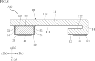
- FIG. 5 to 8 show a semiconductor device according to a second embodiment of the present disclosure.
- FIG. 5 is a plan view showing a semiconductor device A20 of this embodiment.
- FIG. 6 is a right side view of the semiconductor device A20.
- FIG. 7 is a bottom view of the semiconductor device A20.
- FIG. 8 is a cross-sectional view taken along line VIII-VIII in FIG. 5.
- elements that are the same as or similar to those in the above embodiment are given the same reference numerals as those in the above embodiment, and duplicated explanations will be omitted.
- the semiconductor device A20 differs from the above embodiment in the configuration of the conductive support member 10.
- the conductive support member 10 includes a first portion 11, a second portion 12, and a fourth portion 14. As shown in Figures 6 and 8, the first portion 11, the second portion 12, and the fourth portion 14 are appropriately bent and connected when viewed in the second direction y.
- the fourth portion 14 is connected to the end of the first portion 11 on the x1 side in the first direction x.
- the fourth portion 14 is connected to the end of the second portion 12 on the x1 side in the first direction x.
- the first portion 11 and the second portion 12 overlap in the thickness direction z.
- the first portion 11, the second portion 12, and the fourth portion 14 are bent in a folded-back manner.
- the semiconductor device A20 includes a conductive support member 10, a first semiconductor element 20 arranged on the z1 side of the conductive support member 10 in the thickness direction z, and a first mounting portion 41 and a second mounting portion 42.
- the first mounting portion 41 and the second mounting portion 42 are spaced apart from each other in the first direction x.
- the first semiconductor element 20 has a first element main surface 21 facing the z1 side of the thickness direction z and a first element back surface 22 facing the z2 side of the thickness direction z.
- the first mounting portion 41 is arranged on the first element main surface 21 and is conductive to the conductive support member 10.
- the second mounting portion 42 is arranged on the z1 side of the thickness direction z of the conductive support member 10 and is conductive to the conductive support member 10.
- the first mounting portion 41 and the second mounting portion 42 are located on the same side (the z1 side of the thickness direction z) of the conductive support member 10 in the thickness direction z.
- the conductive path of the first semiconductor element 20 is formed by a single conductive support member 10. This allows the semiconductor device A20 to have a simplified structure and reduce manufacturing costs.
- the conductive support member 10 includes a first portion 11 and a second portion 12.
- the first portion 11 has a first main surface 111 facing the z1 side in the thickness direction z.
- the second portion 12 has a second main surface 121 facing the z1 side in the thickness direction z.
- the second main surface 121 is located on the z1 side of the thickness direction z relative to the first main surface 111 in the thickness direction z.
- the first semiconductor element 20 is disposed on the first main surface 111, and the second mounting portion 42 is disposed on the second main surface 121. With this configuration, the positions of the first mounting portion 41 disposed on the first element main surface 21 of the first semiconductor element 20 and the second mounting portion 42 disposed on the second main surface 121 in the thickness direction z can be aligned.
- the conductive support member 10 is made of a metal plate material and further includes a fourth portion 14.
- the second portion 12 is located on the z1 side of the first portion 11 in the thickness direction z.
- the fourth portion 14 is connected to the end of the first portion 11 on the x1 side in the first direction x and the end of the second portion 12 on the x1 side in the first direction x.
- the first portion 11 and the second portion 12 overlap in the thickness direction z.
- the conductive support member 10 having such a configuration can be easily formed by bending a metal plate material in a folded shape.
- the semiconductor device A20 has the same effects as the semiconductor device A10 of the above embodiment.
- Fig. 9 shows a semiconductor device according to a first modification of the second embodiment.
- Fig. 9 is a cross-sectional view showing a semiconductor device A21 of this modification, and corresponds to the cross section shown in Fig. 8.
- the semiconductor device A21 further includes an insulating film 50, which differs from the semiconductor device A20.
- the insulating film 50 covers the z2 side of the conductive support member 10 in the thickness direction z. In the illustrated example, the insulating film 50 covers the entire or substantially the entire first back surface 112 of the first portion 11.
- the constituent material of the insulating film 50 is not particularly limited, and examples include polyimide resin.
- the semiconductor device A21 can suppress undue short circuits and the like caused by contact with the outside.
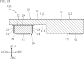
- FIG. 10 is a plan view showing a semiconductor device A30 of this embodiment.
- Fig. 11 is a right side view of the semiconductor device A30.
- Fig. 12 is a bottom view of the semiconductor device A30.
- Fig. 13 is a cross-sectional view taken along line XIII-XIII in Fig. 10.
- the semiconductor device A30 differs from the above embodiment in the configuration of the conductive support member 10.
- the conductive support member 10 includes a first portion 11 and a second portion 12.
- the second portion 12 is connected to the x1 side of the first portion 11 in the first direction x.
- the first back surface 112 of the first portion 11 and the second back surface 122 of the second portion 12 are connected in series.
- the first portion 11 has a stepped shape recessed from the second portion 12 toward the z2 side in the thickness direction z.
- the conductive support member 10 having the stepped shape as described above may be configured to include, unlike the example shown in the figure, an insulating substrate such as a ceramic substrate and a conductive layer formed on the z1 side of the insulating substrate in the thickness direction z.
- the semiconductor device A30 includes a conductive support member 10, a first semiconductor element 20 arranged on the z1 side of the conductive support member 10 in the thickness direction z, and a first mounting portion 41 and a second mounting portion 42.
- the first mounting portion 41 and the second mounting portion 42 are spaced apart from each other in the first direction x.
- the first semiconductor element 20 has a first element main surface 21 facing the z1 side of the thickness direction z and a first element back surface 22 facing the z2 side of the thickness direction z.
- the first mounting portion 41 is arranged on the first element main surface 21 and is electrically connected to the conductive support member 10.
- the second mounting portion 42 is arranged on the z1 side of the thickness direction z of the conductive support member 10 and is electrically connected to the conductive support member 10. With this configuration, the first mounting portion 41 and the second mounting portion 42 are located on the same side (the z1 side of the thickness direction z) of the conductive support member 10 in the thickness direction z.
- the conductive path of the first semiconductor element 20 is formed by a single conductive support member 10. This allows the semiconductor device A30 to have a simplified structure and reduce manufacturing costs.
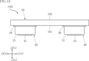
- FIG. 14 is a plan view showing a semiconductor device A40 of this embodiment.
- Fig. 15 is a right side view of the semiconductor device A40.
- Fig. 16 is a bottom view of the semiconductor device A40.
- Fig. 17 is a cross-sectional view taken along line XVII-XVII in Fig. 14.
- the semiconductor device A40 differs from the above embodiment in the configuration of the conductive support member 10.
- the semiconductor device A40 further includes a second semiconductor element 30 and a conductive bonding layer 39.
- the conductive support member 10 is made of a metal plate material as in the above embodiment.
- the conductive support member 10 is a flat plate with a constant or approximately constant thickness as a whole.
- the conductive support member 10 has a main surface 101 and a back surface 102.
- the main surface 101 faces the z1 side in the thickness direction z and faces the first semiconductor element 20 and the second semiconductor element 30.
- the first semiconductor element 20 and the second semiconductor element 30 are supported by the main surface 101.
- the back surface 102 faces the z2 side in the thickness direction z.
- the second semiconductor element 30 is an element that performs the electrical function of the semiconductor device A40. There are no particular limitations on the type of the second semiconductor element 30. In this embodiment, the second semiconductor element 30 is a diode. In this embodiment, the second semiconductor element 30 is rectangular when viewed in the thickness direction z. The second semiconductor element 30 is disposed on the z1 side of the conductive support member 10 in the thickness direction z. The second semiconductor element 30 is located on the x1 side of the first direction x relative to the first semiconductor element 20 in the first direction x.
- the second semiconductor element 30 has a second element main surface 31, a second element back surface 32, a plurality of second element side surfaces 33, and an insulating layer 34.
- the second element main surface 31 and the second element back surface 32 face opposite each other in the thickness direction z.
- the second element main surface 31 faces the z1 side in the thickness direction z.
- the second element back surface 32 faces the z2 side in the thickness direction z.
- an electrode is formed on each of the second element main surface 31 and the second element back surface 32.
- the electrode formed on the second element main surface 31 is a cathode electrode
- the electrode formed on the second element back surface 32 is an anode electrode.
- the second element main surface 31 is located at the same or approximately the same position as the first element main surface 21 of the first semiconductor element 20 in the thickness direction z.
- the second element side surfaces 33 are connected to both the second element main surface 31 and the second element rear surface 32. Any of the second element side surfaces 33 faces the x1 side of the first direction x and the x2 side of the first direction x, and any other of the second element side surfaces 33 (not shown) faces both sides of the second direction y.
- the insulating layer 34 covers at least a part of each of the second element side surfaces 33.
- the specific configuration of the insulating layer 34 is not particularly limited.
- the insulating layer 34 is made of, for example, a Si oxide film (SiO 2 ) that covers the surface of the second element side surface 33.
- the insulating layer 34 is formed, for example, by oxidizing a portion corresponding to the second element side surface 33 during the manufacturing process of the second semiconductor element 30.
- the second semiconductor element 30 may be configured not to have the insulating layer 34.
- the conductive bonding layer 39 is interposed between the second element rear surface 32 of the second semiconductor element 30 and the main surface 101 of the conductive support member 10, and is in contact with both the second element rear surface 32 and the main surface 101.
- the second element rear surface 32 (second semiconductor element 30) is electrically connected to the main surface 101 (conductive support member 10).
- the conductive bonding layer 29 is interposed between the first element rear surface 22 of the first semiconductor element 20 and the main surface 101 of the conductive support member 10, and is in contact with both the first element rear surface 22 and the main surface 101.
- the first element rear surface 22 (first semiconductor element 20) is electrically connected to the main surface 101 (conductive support member 10).
- the first semiconductor element 20 and the second semiconductor element 30 are connected in series via the conductive support member 10.
- the specific configuration of the conductive bonding layer 39 is not particularly limited, and is formed, for example, by firing a paste containing a metal such as silver. Instead of firing a metal paste, the conductive bonding layer 39 may be made of an Au-Si eutectic alloy or solder (a metal containing tin and silver), etc.
- the second mounting portion 42 is disposed on the second element main surface 31 of the second semiconductor element 30, as shown in Figures 15 and 17.
- the second mounting portion 42 covers at least a portion of the second element main surface 31 and is in contact with the second element main surface 31. This allows the second mounting portion 42 to be electrically connected to the conductive support member 10 via the second semiconductor element 30 and the conductive bonding layer 39.
- the second mounting portion 42 is located at the same or approximately the same position as the first mounting portion 41 in the thickness direction z.
- the semiconductor device A40 includes a conductive support member 10, a first semiconductor element 20 arranged on the z1 side of the conductive support member 10 in the thickness direction z, and a first mounting portion 41 and a second mounting portion 42.
- the first mounting portion 41 and the second mounting portion 42 are spaced apart from each other in the first direction x.
- the first semiconductor element 20 has a first element main surface 21 facing the z1 side of the thickness direction z and a first element back surface 22 facing the z2 side of the thickness direction z.
- the first mounting portion 41 is arranged on the first element main surface 21 and is conductive to the conductive support member 10.
- the second mounting portion 42 is arranged on the z1 side of the thickness direction z of the conductive support member 10 and is conductive to the conductive support member 10.
- the first mounting portion 41 and the second mounting portion 42 are located on the same side (the z1 side of the thickness direction z) of the conductive support member 10 in the thickness direction z.
- the conductive path of the first semiconductor element 20 is formed by a single conductive support member 10. This allows the semiconductor device A40 to have a simplified structure and reduce manufacturing costs.
- the semiconductor device A40 further includes a second semiconductor element 30.
- the first semiconductor element 20 (diode) and the second semiconductor element 30 (diode) are connected in series, allowing a large voltage drop. In this way, the semiconductor device A40 can obtain desired electrical characteristics different from those of the above embodiment.
- the semiconductor device A40 achieves the same effects as the semiconductor device A10 within the same range of configuration as the semiconductor device A10 of the above embodiment.
- Figures 18 to 20 show a semiconductor device according to a first modified example of the fourth embodiment.
- Figure 18 is a right side view showing a semiconductor device A41 of this modified example.
- Figure 19 is a bottom view of the semiconductor device A41.
- Figure 20 is a cross-sectional view of the semiconductor device A41, corresponding to the cross section shown in Figure 17.
- the semiconductor device A41 differs from the semiconductor device A40 of the above embodiment in the configuration of the conductive support member 10.
- the conductive support member 10 includes an insulating substrate 10A and a conductive layer 10B.
- the insulating substrate 10A is a flat plate with a constant or approximately constant thickness.
- the insulating substrate 10A has a main surface 101 and a back surface 102.
- the main surface 101 faces the z1 side in the thickness direction z and faces the first semiconductor element 20 and the second semiconductor element 30.
- the first semiconductor element 20 and the second semiconductor element 30 are supported by the main surface 101.
- the back surface 102 faces the z2 side in the thickness direction z.
- the specific configuration of the insulating substrate 10A is not particularly limited, and the insulating substrate 10A is, for example, a ceramic substrate.
- the conductive layer 10B is formed on the main surface 101, which is the z1 side in the thickness direction z of the insulating substrate 10A.
- the conductive layer 10B has a predetermined width in the second direction y and extends in the first direction x.
- the conductive layer 10B covers most of the main surface 101 of the insulating substrate 10A.
- the conductive layer 10B is made of a conductive material.
- the conductive material constituting the conductive layer 10B is not particularly limited. Examples of conductive materials for the conductive layer 10B include those containing silver, copper, gold, etc.
- the method of forming the conductive layer 10B is not limited, and it is formed, for example, by firing a paste containing these metals.
- the conductive bonding layer 29 is interposed between the first element rear surface 22 of the first semiconductor element 20 and the conductive layer 10B, and is in contact with both the first element rear surface 22 and the conductive layer 10B.
- the first element rear surface 22 first semiconductor element 20
- the conductive layer 10B conductive support member 10
- the conductive bonding layer 39 is interposed between the second element rear surface 32 of the second semiconductor element 30 and the conductive layer 10B, and is in contact with both the second element rear surface 32 and the conductive layer 10B.
- the second element rear surface 32 (second semiconductor element 30) is electrically connected to the conductive layer 10B (conductive support member 10).
- the first semiconductor element 20 and the second semiconductor element 30 are connected in series via the conductive layer 10B (conductive support member 10).
- the semiconductor device A41 includes a conductive support member 10, a first semiconductor element 20 arranged on the z1 side of the conductive support member 10 in the thickness direction z, and a first mounting portion 41 and a second mounting portion 42.
- the first mounting portion 41 and the second mounting portion 42 are spaced apart from each other in the first direction x.
- the first semiconductor element 20 has a first element main surface 21 facing the z1 side of the thickness direction z and a first element back surface 22 facing the z2 side of the thickness direction z.
- the first mounting portion 41 is arranged on the first element main surface 21 and is electrically connected to the conductive support member 10.
- the second mounting portion 42 is arranged on the z1 side of the thickness direction z of the conductive support member 10 and is electrically connected to the conductive support member 10. With this configuration, the first mounting portion 41 and the second mounting portion 42 are located on the same side (the z1 side of the thickness direction z) of the conductive support member 10 in the thickness direction z.
- the conductive path of the first semiconductor element 20 is formed by a single conductive support member 10. This allows the semiconductor device A41 to have a simplified structure and reduce manufacturing costs.
- the semiconductor device A41 further includes a second semiconductor element 30.
- the first semiconductor element 20 (diode) and the second semiconductor element 30 (diode) are connected in series, allowing a large voltage drop. This allows the semiconductor device A41 to obtain desired electrical characteristics different from those of the above embodiment.
- the semiconductor device A41 provides the same effects as the semiconductor device A10 within the same range of configuration as the semiconductor device A10 of the above embodiment.
- the conductive support member 10, including the insulating substrate 10A and the conductive layer 10B, may be formed of a printed circuit board.
- the insulating substrate 10A is, for example, a glass epoxy substrate
- the conductive layer 10B is a wiring layer formed on the glass epoxy substrate.
- FIG. 21 to 23 show a semiconductor device according to a second modification of the fourth embodiment.
- Fig. 21 is a plan view showing a semiconductor device A42 of this modification.
- Fig. 22 is a right side view of the semiconductor device A42.
- Fig. 23 is a bottom view of the semiconductor device A42.
- the semiconductor device A42 differs from the semiconductor device A41 in the configuration of the conductive support member 10.
- the semiconductor device A42 includes two first semiconductor elements 20 and two second semiconductor elements 30.
- the insulating substrate 10A has a larger dimension in the second direction y.
- the conductive layer 10B is formed in two regions spaced apart from each other in the second direction y.
- the first semiconductor elements 20 and the second semiconductor elements 30 are arranged corresponding to the conductive layers 10B in the two regions.
- a pair of the first semiconductor elements 20 and the second semiconductor elements 30 on one side of the second direction y are connected in series via the conductive layer 10B (conductive support member 10) formed on one side of the second direction y.
- Another pair of the first semiconductor elements 20 and the second semiconductor elements 30 on the other side of the second direction y are connected in series via the conductive layer 10B (conductive support member 10) formed on the other side of the second direction y.
- the semiconductor device A42 includes a conductive support member 10, a first semiconductor element 20 arranged on the z1 side of the conductive support member 10 in the thickness direction z, and a first mounting portion 41 and a second mounting portion 42.
- the first mounting portion 41 and the second mounting portion 42 are spaced apart from each other in the first direction x.
- the first semiconductor element 20 has a first element main surface 21 facing the z1 side of the thickness direction z and a first element back surface 22 facing the z2 side of the thickness direction z.
- the first mounting portion 41 is arranged on the first element main surface 21 and is conductive to the conductive support member 10.
- the second mounting portion 42 is arranged on the z1 side of the thickness direction z of the conductive support member 10 and is conductive to the conductive support member 10.
- the first mounting portion 41 and the second mounting portion 42 are located on the same side (the z1 side of the thickness direction z) of the conductive support member 10 in the thickness direction z.
- the conductive path of the first semiconductor element 20 is formed by a single conductive support member 10. This allows the semiconductor device A42 to have a simplified structure and reduce manufacturing costs.
- the semiconductor device A42 further includes a second semiconductor element 30.
- the first semiconductor element 20 (diode) and the second semiconductor element 30 (diode) are connected in series, allowing for a large voltage drop.
- two sets of the first semiconductor element 20 and the second semiconductor element 30 are provided, and the first semiconductor element 20 and the second semiconductor element 30 of each set are connected in series to each other.
- the semiconductor device A42 provides the same effects as the semiconductor device A10 within the same range of configuration as the semiconductor device A10 of the above embodiment.
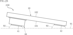
- Fig. 24 shows a semiconductor device according to a fifth embodiment of the present disclosure.
- Fig. 24 is a right side view showing a semiconductor device A50 according to the present embodiment.
- the semiconductor device A50 differs from the semiconductor device A10 of the above embodiment in the configuration of the conductive support member 10.
- the conductive support member 10 is made of a metal plate material as in the above embodiment.
- the conductive support member 10 is a flat plate with a constant or approximately constant thickness.
- the conductive support member 10 has a main surface 101 and a back surface 102.
- the main surface 101 faces the z1 side in the thickness direction z and faces the first semiconductor element 20.
- the first semiconductor element 20 is supported by the main surface 101.
- the back surface 102 faces the z2 side in the thickness direction z.
- the second mounting portion 42 is disposed on the main surface 101.
- the second mounting portion 42 is located on the z2 side of the first mounting portion 41 in the thickness direction z.
- FIG. 25 shows the semiconductor device A50 in use, and is a right side view of the semiconductor device A50 mounted on a circuit board 91.
- Each of the first mounting portion 41 and the second mounting portion 42 is joined to the circuit board 91 via a conductive bonding material 92.
- the bonding material 92 is, for example, solder.
- the semiconductor device A50 can be mounted on the circuit board 91 with the conductive support member 10 tilted relative to the circuit board 91.
- the semiconductor device A50 includes a conductive support member 10, a first semiconductor element 20 arranged on the z1 side of the conductive support member 10 in the thickness direction z, and a first mounting portion 41 and a second mounting portion 42.
- the first mounting portion 41 and the second mounting portion 42 are spaced apart from each other in the first direction x.
- the first semiconductor element 20 has a first element main surface 21 facing the z1 side of the thickness direction z and a first element back surface 22 facing the z2 side of the thickness direction z.
- the first mounting portion 41 is arranged on the first element main surface 21 and is conductive to the conductive support member 10.
- the second mounting portion 42 is arranged on the z1 side of the thickness direction z of the conductive support member 10 and is conductive to the conductive support member 10.
- the first mounting portion 41 and the second mounting portion 42 are located on the same side (the z1 side of the thickness direction z) of the conductive support member 10 in the thickness direction z.
- the conductive path of the first semiconductor element 20 is formed by a single conductive support member 10. This allows the semiconductor device A50 to have a simplified structure and reduce manufacturing costs.
- the semiconductor device A50 has the same effects as the semiconductor device A10 within the same range of configuration as the semiconductor device A10 of the above embodiment.
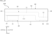
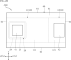
- FIG. 26 to 29 show a semiconductor device according to a sixth embodiment of the present disclosure.
- Fig. 26 is a plan view showing a semiconductor device A60 of this embodiment.
- Fig. 27 is a right side view of the semiconductor device A60.
- Fig. 28 is a bottom view of the semiconductor device A60.
- Fig. 29 is a cross-sectional view taken along line XXIX-XXIX in Fig. 26.
- the semiconductor device A60 further includes a sealing resin 60, which is different from the semiconductor device A10 of the above embodiment.
- the sealing resin 60 covers at least a portion of the conductive support member 10, the first semiconductor element 20, and a portion of each of the first mounting portion 41 and the second mounting portion 42. As shown in FIG. 29, in the semiconductor device A60, the first semiconductor element 20 does not have an insulating layer 24, and the first element side surface 23 is covered with the sealing resin 60.
- the sealing resin 60 has a resin main surface 61, a resin back surface 62, a pair of first resin side surfaces 63, and a pair of second resin side surfaces 64.
- the constituent material of the sealing resin 60 is, for example, a black epoxy resin.
- the resin main surface 61 faces the same side as the first main surface 111 of the conductive support member 10 (first portion 11) in the thickness direction z.
- the resin main surface 61 faces the z1 side in the thickness direction z.
- the resin back surface 62 faces the opposite side to the resin main surface 61.
- the resin back surface 62 faces the z2 side in the thickness direction z.
- the first mounting portion 41 and the second mounting portion 42 are exposed from the resin main surface 61.
- the mounting surface 411 facing the z1 side in the thickness direction z of the first mounting portion 41 and the mounting surface 421 facing the z2 side in the thickness direction z of the second mounting portion 42 are exposed from the resin main surface 61.
- the mounting surface 411 and the mounting surface 421 are flush with the resin main surface 61.
- the pair of first resin side surfaces 63 are connected to both the resin main surface 61 and the resin back surface 62, and face the first direction x.
- the pair of first resin side surfaces 63 are spaced apart from each other in the first direction x.
- the end surface 113 of the first part 11 facing the x2 side of the first direction x is exposed from the first resin side surface 63 facing the x2 side of the first direction x so as to be flush with the first resin side surface 63.
- the end surface 123 of the second part 12 facing the x1 side of the first direction x is exposed from the first resin side surface 63 facing the x1 side of the first direction x so as to be flush with the first resin side surface 63.
- the pair of second resin side surfaces 64 are connected to all of the resin main surface 61, the resin back surface 62, and the pair of first resin side surfaces 63, and face the second direction y.
- the pair of second resin side surfaces 64 are spaced apart from each other in the second direction y.
- the semiconductor device A60 includes a conductive support member 10, a first semiconductor element 20 arranged on the z1 side of the conductive support member 10 in the thickness direction z, and a first mounting portion 41 and a second mounting portion 42.
- the first mounting portion 41 and the second mounting portion 42 are spaced apart from each other in the first direction x.
- the first semiconductor element 20 has a first element main surface 21 facing the z1 side of the thickness direction z and a first element back surface 22 facing the z2 side of the thickness direction z.
- the first mounting portion 41 is arranged on the first element main surface 21 and is electrically connected to the conductive support member 10.
- the second mounting portion 42 is arranged on the z1 side of the thickness direction z of the conductive support member 10 and is electrically connected to the conductive support member 10. With this configuration, the first mounting portion 41 and the second mounting portion 42 are located on the same side (the z1 side of the thickness direction z) of the conductive support member 10 in the thickness direction z.
- the conductive path of the first semiconductor element 20 is formed by a single conductive support member 10. This allows the semiconductor device A60 to have a simplified structure and reduce manufacturing costs.
- the conductive support member 10 includes a first portion 11 and a second portion 12.
- the first portion 11 has a first main surface 111 facing the z1 side of the thickness direction z.
- the second portion 12 has a second main surface 121 facing the z1 side of the thickness direction z.
- the second main surface 121 is located on the z1 side of the thickness direction z with respect to the first main surface 111 in the thickness direction z.
- the first semiconductor element 20 is disposed on the first main surface 111, and the second mounting portion 42 is disposed on the second main surface 121. With this configuration, the positions of the first mounting portion 41 disposed on the first element main surface 21 of the first semiconductor element 20 and the second mounting portion 42 disposed on the second main surface 121 in the thickness direction z can be aligned.
- the semiconductor device A60 has the same effects as the semiconductor device A10 within the same range of configuration as the semiconductor device A10 of the above embodiment.
- the semiconductor device according to the present disclosure is not limited to the above-mentioned embodiment.
- the specific configuration of each part of the semiconductor device according to the present disclosure can be freely designed in various ways.
- the second mounting portion 42 is disposed on the surface (second main surface 121 or main surface 101) of the conductive support member 10 facing the z1 side in the thickness direction z, but the present disclosure is not limited to this.
- the conductive support member 10 is made of a metal plate or the like, a portion of the conductive support member 10 including a surface facing the z1 side in the thickness direction z may serve as the second mounting portion without providing a separate second mounting portion 42.
- Appendix 1 A conductive support member; a first semiconductor element disposed on one side of the conductive support member in a thickness direction; a first mounting portion and a second mounting portion spaced apart from each other in a direction perpendicular to the thickness direction, the first semiconductor element has a first element main surface facing one side in the thickness direction and a first element back surface facing the other side in the thickness direction, the first mounting portion is disposed on the first element main surface and is electrically connected to the conductive support member; The second mounting portion is disposed on one side of the conductive support member in the thickness direction and is electrically connected to the conductive support member.
- the first semiconductor element has a first element side surface connected to the first element main surface and the first element back surface, and an insulating layer covering at least a portion of the first element side surface.
- the conductive support member includes a first portion having a first main surface facing one side in the thickness direction, and a second portion having a second main surface facing one side in the thickness direction, the second main surface is located on one side in the thickness direction with respect to the first main surface, the first semiconductor element is disposed on the first main surface, 3.
- the second mounting portion is disposed on the second main surface.
- the second portion is located on one side in the thickness direction with respect to the first portion, The semiconductor device according to claim 3, wherein the second mounting portion is located on one side of the first mounting portion in a first direction perpendicular to the thickness direction.
- the conductive support member includes a third portion connected to one end of the first portion in the first direction and to the other end of the second portion in the first direction, The semiconductor device according to claim 4, wherein the first portion and the second portion do not overlap when viewed in the thickness direction.
- the conductive support member includes a fourth portion connected to one end of the first portion in the first direction and to one end of the second portion in the first direction, The semiconductor device according to claim 4, wherein the first portion and the second portion overlap when viewed in the thickness direction.
- the conductive support member is made of a metal plate. Appendix 8. 8. The semiconductor device according to claim 3, wherein a constituent material of the conductive support member includes copper. Appendix 9. 4. The semiconductor device according to claim 1, wherein the conductive support member includes an insulating substrate and a conductive layer formed on one side of the insulating substrate in the thickness direction. Appendix 10. 10. The semiconductor device according to claim 9, wherein the insulating substrate is a ceramic substrate. Appendix 11. 10. The semiconductor device according to claim 9, wherein the conductive support member is formed of a printed circuit board. Appendix 12.
- a second semiconductor element disposed on one side of the conductive support member in the thickness direction; the second semiconductor element has a second element main surface facing one side in the thickness direction and a second element back surface facing the other side in the thickness direction, 3.
- the semiconductor device according to claim 1 wherein the second mounting portion is disposed on the second element main surface.
- Appendix 13 9. The semiconductor device according to claim 1, wherein a constituent material of each of the first mounting portion and the second mounting portion includes gold.
- Appendix 14 9. The semiconductor device according to claim 3, further comprising a sealing resin covering at least a portion of the conductive support member and the first semiconductor element, the first mounting portion and the second mounting portion being exposed from the sealing resin.
- Appendix 15. 9. The semiconductor device according to claim 1, further comprising an insulating film covering the other side of the conductive support member in the thickness direction.
Landscapes
- Engineering & Computer Science (AREA)
- Microelectronics & Electronic Packaging (AREA)
- Structures Or Materials For Encapsulating Or Coating Semiconductor Devices Or Solid State Devices (AREA)
Priority Applications (1)
| Application Number | Priority Date | Filing Date | Title |
|---|---|---|---|
| JP2024574409A JPWO2024161996A1 (https=) | 2023-02-01 | 2024-01-17 |
Applications Claiming Priority (2)
| Application Number | Priority Date | Filing Date | Title |
|---|---|---|---|
| JP2023013713 | 2023-02-01 | ||
| JP2023-013713 | 2023-02-01 |
Publications (1)
| Publication Number | Publication Date |
|---|---|
| WO2024161996A1 true WO2024161996A1 (ja) | 2024-08-08 |
Family
ID=92146571
Family Applications (1)
| Application Number | Title | Priority Date | Filing Date |
|---|---|---|---|
| PCT/JP2024/001083 Ceased WO2024161996A1 (ja) | 2023-02-01 | 2024-01-17 | 半導体装置 |
Country Status (2)
| Country | Link |
|---|---|
| JP (1) | JPWO2024161996A1 (https=) |
| WO (1) | WO2024161996A1 (https=) |
Citations (3)
| Publication number | Priority date | Publication date | Assignee | Title |
|---|---|---|---|---|
| JP2011204862A (ja) * | 2010-03-25 | 2011-10-13 | Sanyo Electric Co Ltd | 半導体装置およびその製造方法 |
| WO2016203764A1 (ja) * | 2015-06-17 | 2016-12-22 | パナソニックIpマネジメント株式会社 | 半導体装置及びモジュール部品 |
| WO2020218298A1 (ja) * | 2019-04-24 | 2020-10-29 | ローム株式会社 | 半導体装置 |
-
2024
- 2024-01-17 WO PCT/JP2024/001083 patent/WO2024161996A1/ja not_active Ceased
- 2024-01-17 JP JP2024574409A patent/JPWO2024161996A1/ja active Pending
Patent Citations (3)
| Publication number | Priority date | Publication date | Assignee | Title |
|---|---|---|---|---|
| JP2011204862A (ja) * | 2010-03-25 | 2011-10-13 | Sanyo Electric Co Ltd | 半導体装置およびその製造方法 |
| WO2016203764A1 (ja) * | 2015-06-17 | 2016-12-22 | パナソニックIpマネジメント株式会社 | 半導体装置及びモジュール部品 |
| WO2020218298A1 (ja) * | 2019-04-24 | 2020-10-29 | ローム株式会社 | 半導体装置 |
Also Published As
| Publication number | Publication date |
|---|---|
| JPWO2024161996A1 (https=) | 2024-08-08 |
Similar Documents
| Publication | Publication Date | Title |
|---|---|---|
| JP7520177B2 (ja) | 半導体装置 | |
| CN100562999C (zh) | 电路模块 | |
| US7839003B2 (en) | Semiconductor device including a coupling conductor having a concave and convex | |
| JP7503058B2 (ja) | 電子装置および電子装置の実装構造 | |
| US9024446B2 (en) | Element mounting substrate and semiconductor module | |
| JP3660663B2 (ja) | チップパッケージの製造方法 | |
| US6833512B2 (en) | Substrate board structure | |
| CN101499454B (zh) | 配线电路基板及其制造方法 | |
| JP2012212712A (ja) | 半導体装置の実装構造及び半導体装置の実装方法 | |
| WO2024161996A1 (ja) | 半導体装置 | |
| JP7022541B2 (ja) | 半導体装置 | |
| JP3251688B2 (ja) | 半導体素子搭載用リードフレーム | |
| JP2006310277A (ja) | チップ型ヒューズ | |
| US11830641B2 (en) | Chip resistor component | |
| JP4329187B2 (ja) | 半導体素子 | |
| WO2020004459A1 (ja) | 電子素子搭載用基板、電子装置および電子モジュール | |
| WO2012129118A1 (en) | Circuit protection device | |
| JP2024096564A (ja) | 電気機器および電気機器の製造方法 | |
| JP6254807B2 (ja) | 半導体装置および電子機器 | |
| WO2024101174A1 (ja) | 半導体装置 | |
| JP2005310957A (ja) | 表示装置 | |
| JP2545077Y2 (ja) | チツプ形抵抗器 | |
| JPH05326814A (ja) | 電子回路素子搭載用リードフレーム | |
| JP2865400B2 (ja) | 混成集積回路装置 | |
| WO2024262239A1 (ja) | 電子装置 |
Legal Events
| Date | Code | Title | Description |
|---|---|---|---|
| 121 | Ep: the epo has been informed by wipo that ep was designated in this application |
Ref document number: 24749950 Country of ref document: EP Kind code of ref document: A1 |
|
| ENP | Entry into the national phase |
Ref document number: 2024574409 Country of ref document: JP Kind code of ref document: A |
|
| WWE | Wipo information: entry into national phase |
Ref document number: 2024574409 Country of ref document: JP |
|
| NENP | Non-entry into the national phase |
Ref country code: DE |
|
| 122 | Ep: pct application non-entry in european phase |
Ref document number: 24749950 Country of ref document: EP Kind code of ref document: A1 |