WO2024157752A1 - 半導体装置の製造方法および半導体装置 - Google Patents
半導体装置の製造方法および半導体装置 Download PDFInfo
- Publication number
- WO2024157752A1 WO2024157752A1 PCT/JP2024/000157 JP2024000157W WO2024157752A1 WO 2024157752 A1 WO2024157752 A1 WO 2024157752A1 JP 2024000157 W JP2024000157 W JP 2024000157W WO 2024157752 A1 WO2024157752 A1 WO 2024157752A1
- Authority
- WO
- WIPO (PCT)
- Prior art keywords
- recess
- semiconductor device
- pad
- semiconductor element
- bonding material
- Prior art date
- Legal status (The legal status is an assumption and is not a legal conclusion. Google has not performed a legal analysis and makes no representation as to the accuracy of the status listed.)
- Ceased
Links
Images







Classifications
-
- H—ELECTRICITY
- H10—SEMICONDUCTOR DEVICES; ELECTRIC SOLID-STATE DEVICES NOT OTHERWISE PROVIDED FOR
- H10W—GENERIC PACKAGES, INTERCONNECTIONS, CONNECTORS OR OTHER CONSTRUCTIONAL DETAILS OF DEVICES COVERED BY CLASS H10
- H10W72/00—Interconnections or connectors in packages
-
- H—ELECTRICITY
- H10—SEMICONDUCTOR DEVICES; ELECTRIC SOLID-STATE DEVICES NOT OTHERWISE PROVIDED FOR
- H10W—GENERIC PACKAGES, INTERCONNECTIONS, CONNECTORS OR OTHER CONSTRUCTIONAL DETAILS OF DEVICES COVERED BY CLASS H10
- H10W72/00—Interconnections or connectors in packages
- H10W72/071—Connecting or disconnecting
Definitions
- This disclosure relates to a semiconductor device.
- the chip is mounted on one side of the lead frame and is electrically connected to the lead frame via a solder layer, which also fixes the chip in place.
- One of the objectives of this disclosure is to provide a semiconductor device that is an improvement over conventional semiconductor devices.
- one of the objectives of this disclosure is to provide a semiconductor device that can improve reliability against temperature cycles.
- a semiconductor device provided by one aspect of the present disclosure includes a support member having a first surface, a semiconductor element having a second surface, and a bonding material.
- the first surface or the second surface has a recess and a flat portion.
- the bonding material is filled in the recess.
- the first surface and the second surface are electrically bonded by the bonding material.
- the above configuration makes it possible to improve reliability against temperature cycles.
- FIG. 1 is a perspective view showing a semiconductor device according to a first embodiment of the present disclosure
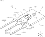
- FIG. 2 is a perspective view of the semiconductor device shown in FIG. 1 , with a sealing resin omitted.
- 1 is a plan view showing a semiconductor device according to a first embodiment of the present disclosure.
- FIG. 4 is a cross-sectional view taken along line IV-IV in FIG. 4 is a cross-sectional view taken along line VV in FIG. 3.
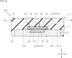
- 1 is a cross-sectional view showing a first modified example of the semiconductor device according to the first embodiment of the present disclosure.
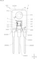
- FIG. 11 is a plan view showing a second modified example of the semiconductor device according to the first embodiment of the present disclosure.
- 8 is a cross-sectional view taken along line VIII-VIII in FIG.
- FIG. 13 is a plan view showing a third modified example of the semiconductor device according to the first embodiment of the present disclosure.
- 10 is a cross-sectional view taken along line XX of FIG. 9 , showing a third modified example of the semiconductor device according to the first embodiment of the present disclosure.
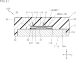
- FIG. 4 is a cross-sectional view showing a semiconductor device according to a second embodiment of the present disclosure.
- FIG. 11 is a cross-sectional view showing a semiconductor device according to a third embodiment of the present disclosure.
- First embodiment: 1 to 5 show a semiconductor device A10 according to a first embodiment of the present disclosure.
- the semiconductor device A10 according to the present disclosure is of a type that is surface-mounted on an electrical circuit board of, for example, an automobile, electronic device, or the like.
- the semiconductor device A10 includes a semiconductor element 1, a lead frame 2, a bonding material 3, a wire 4, and a sealing resin 5.
- the wire 4 includes a first wire 41 and a second wire 42.
- the semiconductor device according to the present disclosure is not limited to a configuration that includes the wire 4, and may include a conductive member formed, for example, using a metal plate material instead of the wire 4.
- FIG. 1 is a perspective view of the semiconductor device A10.
- FIG. 2 is a perspective view of FIG. 1 with the sealing resin 5 omitted.
- FIG. 3 is a plan view of the semiconductor device A10.
- FIG. 4 is a cross-sectional view taken along line IV-IV in FIG. 3.
- FIG. 5 is a cross-sectional view taken along line V-V in FIG. 3. Note that the sealing resin 5 is shown through FIG. 3.
- the thickness direction of the semiconductor device A10 is defined as the first direction z
- the up-down direction in the plan view (FIG. 3) perpendicular to the first direction z is defined as the second direction x
- the left-right direction in the plan view FIG.
- the semiconductor element 1 is a circuit element made of semiconductor material, and is the core element of the function of the semiconductor device A10. Specific examples of the semiconductor element 1 are not limited in any way, and may be, for example, an IGBT (Insulated Gate Bipolar Transistor), a MOSFET (Metal-Oxide-Semiconductor Field Effect Transistor), a diode, etc. In this embodiment, the semiconductor element 1 is an IGBT (Insulated Gate Bipolar Transistor). As shown in FIG. 4, the semiconductor element 1 has a semiconductor element main surface 111 and a semiconductor element back surface 112.
- the semiconductor element main surface 111 is the upper surface of the semiconductor element 1.
- the semiconductor element back surface 112 is the lower surface of the semiconductor element 11.
- the semiconductor element back surface 112 corresponds to the "second surface” of this disclosure.
- the semiconductor element main surface 111 and the semiconductor element back surface 112 face in opposite directions to each other in the first direction z.
- Part of the semiconductor element main surface 111 is a first electrode pad 113 and a second electrode pad 114.
- the area of the first electrode pad 113 is smaller than the area of the second electrode pad 114.
- the first electrode pad 113 is the gate electrode of the IGBT
- the second electrode pad 114 is the emitter electrode of the IGBT.
- the main part of the semiconductor element rear surface 112 is a third electrode pad 115.
- the third electrode pad 115 is the collector electrode of the IGBT.
- the semiconductor element 1 has a rectangular shape when viewed in the thickness direction (first direction z).
- the dimensions of the semiconductor element 1 when viewed in the first direction z are 1 mm to 10 mm square.
- the dimensions of the semiconductor element 1 in the thickness direction are 40 ⁇ m to 300 ⁇ m.
- the lead frame 2 is a conductive member, and by being joined to the circuit board, forms a conductive path between the semiconductor device A10 and the circuit board.
- the lead frame 2 is made of an alloy mainly composed of Cu. Note that a part of the surface may be plated in consideration of corrosion resistance, electrical conductivity, thermal conductivity, or joinability.
- the lead frame 2 has a first lead 21, a second lead 22, and a third lead 23.
- the first lead 21 corresponds to the "support member" in this disclosure.
- the first lead 21 includes a first pad 211 (die pad), a first terminal 212, and an intermediate connection portion 213.
- the material of the first lead 21 includes copper, nickel, iron, etc.
- the first pad 211 has a pad main surface 211a and a pad back surface 211b.
- the pad main surface 211a is the upper surface of the first pad 211.
- the pad main surface 211a corresponds to the "first surface” of this disclosure.
- the pad main surface 211a is the surface on which the semiconductor element 1 is mounted, and as shown in FIG. 4, the semiconductor element back surface 112 faces the pad main surface 211a.
- the pad back surface 211b is the lower surface of the first pad 211. Both the pad main surface 211a and the pad back surface 211b are flat and face opposite each other in the first direction z.
- the pad main surface 211a includes a first recess 215 and a first flat portion 216.
- the first flat portion 216 is a flat portion, and in this embodiment, is perpendicular to the first direction z.
- the first recess 215 is recessed in the first direction z from the first flat portion 216, and is an example of a "recess" in this disclosure.
- the first recess 215 includes a first recess bottom surface 215a and a first recess circumferential surface 215b.
- the first recess bottom surface 215a is the surface located at the deepest part in the depth direction (first direction z) of the first recess 215.
- the first recess circumferential surface 215b is located between the first recess bottom surface 215a and the first flat portion 216.
- the area of the first recess 215 in a plan view i.e., the area surrounded by the side where the first recess circumferential surface 215b and the first flat portion 216 intersect, is smaller than the area of the semiconductor element back surface 112.
- the first recess 215 is contained within the semiconductor element 1.
- a portion of the first flat portion 216 overlaps with the semiconductor element 1.
- the first recess bottom surface 215a is assumed to be rectangular, but may be triangular, polygonal, circular, or other shapes.
- the angle ⁇ between the first recess bottom surface 215a and the first recess circumferential surface 215b is approximately 45 degrees.
- the depth of the first recess 215 is not particularly limited, but is approximately 10 ⁇ m to 650 ⁇ m. The thicker the first pad 211, the deeper the first recess 215 can be.
- a pad through hole 211c is formed in the first pad 211, which extends from the pad main surface 211a to the pad back surface 211b.
- the pad through hole 211c is spaced apart from the semiconductor element 1 when viewed in the thickness direction.
- the pad through hole 211c is circular when viewed in the thickness direction, but the shape is not limited thereto.
- the first terminal 212 extends along the second direction x and is partially exposed from the sealing resin 5.
- the first terminal 212 is electrically connected to the third electrode pad 115 via the intermediate connecting portion 213, the first pad 211, and the bonding material 3.
- the third electrode pad 115 is a collector electrode, and therefore the first terminal 212 is the collector terminal of the semiconductor device A1.
- the intermediate connecting portion 213 is a portion that connects the first pad 211 and the first terminal 212. As shown in Figure 5, the positions of the first pad 211 and the first terminal 212 are different in the first direction z, and the first pad 211 is located lower than the first terminal 212 in Figure 5. Therefore, the intermediate connecting portion 213 is inclined with respect to the first pad 211 and the first terminal 212. The entire intermediate connecting portion 213 is covered with the sealing resin 5.
- the second lead 22 is a member that is spaced apart from the first lead 21 and extends along the second direction x. In the third direction y, the second lead 22 is located on one side of the first terminal 212.
- the second lead 22 includes a second pad 221 and a second terminal 222.
- the second pad 221 is longer in the third direction y than the second terminal 222, and is entirely covered with the sealing resin 5. As shown in FIGS. 2 and 3, the first wire 41 is connected to the second pad 221.
- the second terminal 222 extends along the second direction x and is partially exposed from the sealing resin 5.
- the second terminal 222 is electrically connected to the first electrode pad 113 via the second pad 221 and the first wire 41.
- the first electrode pad 113 is a gate electrode, and therefore the second terminal 222 is a gate terminal of the semiconductor device A1.
- the third lead 23 is a member that is spaced apart from the first lead 21 and the second lead 22 and extends along the second direction x. In the third direction y, the third lead 23 is located on the opposite side of the first terminal 212 from the second lead 22.
- the third lead 23 includes a third pad 231 and a third terminal 232.
- the third pad 231 is a portion that is longer in the third direction y than the third pad 231 and is entirely covered with the sealing resin 5. As shown in FIGS. 2 and 3, a second wire 42 is connected to the third pad 231.
- the third terminal 232 extends along the second direction x and is partially exposed from the sealing resin 5.
- the third terminal 232 is electrically connected to the second electrode pad 114 via the third pad 231 and the second wire 42.
- the second electrode pad 114 is an emitter electrode, and therefore the third terminal 232 is the emitter terminal of the semiconductor device A10.
- the portions of the first terminal 212, the second terminal 222, and the third terminal 232 that are exposed from the sealing resin 5 may be covered with plating. By covering these with plating, corrosion resistance can be improved.
- the bonding material 3 is a conductive material that is interposed between the semiconductor element 1 and the first pad 211 of the first lead 21.
- the bonding material 3 includes a thick portion 31 and a thin portion 32.
- the thick portion 31 fills the first recess 215.
- the thin portion 32 is interposed between the back surface 112 of the semiconductor element and the first flat portion 216.
- the thickness of the thick portion 31 is about 15 ⁇ m to 750 ⁇ m, and the thickness of the thin portion 32 is about 10 ⁇ m to 120 ⁇ m.
- the thickness of the thick portion 31 is the sum of the thickness of the thin portion 32 and the depth of the first recess 215.
- the bonding material 3 mounts the semiconductor element 1 on the first pad 211 and ensures electrical continuity between the third electrode pad 115 of the semiconductor element 1 and the first lead 21. Any conductive material such as solder or silver paste can be used as the bonding material 3.
- the first wire 41 and the second wire 42 are made of the same metal and are conductive members.
- the first wire 41 and the second wire 42 are made of Al (aluminum) or an Al alloy.
- one end of the first wire 41 is bonded to the second pad 221, and the other end is bonded to the first electrode pad 113 on the semiconductor element main surface 111.
- the first wire 41 provides electrical conductivity between the second pad 221 and the first electrode pad 113.
- one end of the second wire 42 is bonded to the third pad 231, and the other end is bonded to the second electrode pad 114 on the semiconductor element main surface 111. Therefore, the second wire 42 provides electrical conductivity between the third pad 231 and the second electrode pad 114.
- the sealing resin 5 is a member that covers a part of the lead frame 2, the semiconductor element 1, the first wire 41, and the second wire 42.
- the sealing resin 5 is a thermosetting synthetic resin that has electrical insulation properties. In this embodiment, it is a black epoxy resin.
- the sealing resin 5 has a resin main surface 51, a resin back surface 52, a pair of resin first side surfaces 53, and a pair of resin second side surfaces 54.
- the resin main surface 51 is the upper surface of the sealing resin 5 shown in Figures 4 and 5.
- the resin back surface 52 is the lower surface of the sealing resin 5 shown in Figures 4 and 5.
- the resin main surface 51 and the resin back surface 52 face in opposite directions to each other in the first direction z.
- the pair of resin first side surfaces 53 are surfaces formed at a distance from each other in the second direction x, as shown in FIG. 5.
- the pair of resin first side surfaces 53 face opposite each other in the second direction x.
- the upper end of the resin first side surface 53 shown in FIG. 5 is connected to the resin main surface 51, and the lower end of the resin first side surface 53 shown in FIG. 5 is connected to the resin back surface 52.
- a portion of each of the first lead 21 (first terminal 212) and the second lead 22 (second terminal 222) is exposed from one of the resin first side surfaces 53.
- the pair of resin second side surfaces 54 are surfaces formed at a distance in the third direction y as shown in FIG. 4.
- the pair of resin second side surfaces 54 face opposite each other in the third direction y.
- the upper end of the resin second side surface 54 shown in FIG. 4 is connected to the resin main surface 51, and the lower end of the resin second side surface 54 shown in FIG. 4 is connected to the resin back surface 52.
- the sealing resin 5 has a pair of recesses 55 recessed into the sealing resin 5 from the upper portions of the pair of resin second side surfaces 54 shown in FIG. 1. Also, as shown in FIGS. 1 and 5, in the first direction z, the sealing resin 5 has a resin through hole 56 formed from the resin main surface 51 to the resin back surface 52. In this embodiment, the center of the resin through hole 56 is the same (or approximately the same) as the center of the pad through hole 211c. Also, the diameter of the resin through hole 56 is smaller than the diameter of the pad through hole 211c. In this embodiment, the hole walls of the pad through hole 211c are all covered with the sealing resin 5.
- FIGS. 6 to 12 show modified examples and other embodiments of the present disclosure.
- elements that are the same as or similar to those in the above-described embodiment are given the same reference numerals as in the above-described embodiment.
- the configurations of the various parts in each modified example and each embodiment can be combined with each other as appropriate to the extent that no technical contradictions arise.
- First Modification of First Embodiment 6 shows a first modified example of the semiconductor device A10.
- the shape of the first recess 215 is different from that of the semiconductor device A10.
- the angle between the first recess bottom surface 215a and the first recess circumferential surface 215b is approximately 90 degrees.
- the volume of the bonding material 3 is increased, so the stress generated in the bonding material 3 is reduced.
- the angle between the bottom surface 215a of the first recess and the peripheral surface 215b of the first recess is arbitrary.
- Second Modification of First Embodiment shows a second modified example of the semiconductor device A10.
- the configuration of the first recess 215 is different from that of the semiconductor device A10.
- the first recess 215 includes a plurality of regions 217. Specifically, the plurality of regions 217 are separated from one another in a plan view, and a portion of the first flat portion 216 is present between each of the regions 217. There is no limitation on the number of the plurality of regions 217, and in the illustrated example, there are four. Correspondingly, the first recess 215 has four first recess bottom surfaces 215a. As can be seen from this modified example, the first recess 215 may be configured to include a plurality of regions 217 that are separated from one another. In the illustrated example, the shape of the regions 217 is rectangular, but other shapes are also possible. In FIG. 7, the four regions 217 are arranged in two rows and two columns, but the arrangement is also arbitrary.
- the first recess 215 includes a region 217 and a plurality of regions 218.
- the region 217 and the plurality of regions 218 are connected to each other.
- the region 217 overlaps the semiconductor element back surface 112 and is contained within the semiconductor element back surface 112.
- the plurality of regions 218 are arranged so as to overlap the four corners of the semiconductor element back surface 112.
- the plurality of regions 218 are connected to the four corners of the region 217.
- the thick portion 31 is filled in the region 217 and the region 218. That is, a portion of the region 218 overlaps the semiconductor element back surface 112 in a plan view, and another portion protrudes from the semiconductor element back surface 112.
- the region 217 and the plurality of regions 218 are rectangular in a plan view, but the shape is arbitrary.
- This modification also increases the volume of the bonding material 3, making it possible to reduce the stress in the bonding material 3 below the semiconductor element 1. Furthermore, according to the inventors' analysis, significant stress concentration was observed in the portions of the bonding material 3 located directly below the four corners of the semiconductor element 1. In this modification, multiple regions 218 exist at the four corners of the semiconductor element 1. For this reason, multiple thick portions 31 are arranged at the four corners of the semiconductor element 1. This makes it possible to more efficiently alleviate the stress concentration in the bonding material 3 at the four corners of the semiconductor element 1. Furthermore, a first flat portion 216 is provided in the areas other than the region 217 and the multiple regions 218. This makes it possible to properly support the semiconductor element 1.
- FIG. 11 shows a semiconductor device according to the second embodiment of the present disclosure.
- the semiconductor element back surface 112 includes a second recess 117 and a second flat portion 118.
- the second flat portion 118 is a flat portion, and in this embodiment, is perpendicular to the first direction z.
- the second recess 117 is recessed in the first direction z from the second flat portion 118, and is an example of a "recess" in this disclosure.
- the second recess 117 includes a second recess bottom surface 117a and a second recess circumferential surface 117b.
- the second recess bottom surface 117a is the surface located at the deepest part in the depth direction (first direction z) of the second recess 117.
- the second recess circumferential surface 117b is located between the second recess bottom surface 117a and the second flat portion 118.
- the second recess bottom surface 117a is assumed to be rectangular, but may be another shape such as a triangular shape, a polygonal shape, or a circle.
- the angle formed by the second recess bottom surface 117a and the second recess circumferential surface 117b is arbitrary.
- the depth of the second recess 117 is not particularly limited, but is about 1 ⁇ m to 230 ⁇ m. Note that the thicker the semiconductor element 1 is, the deeper the second recess 117 can be.
- the thick portion 31 is filled in the second recess 117.
- the thick portion 31 can be formed, so that the stress of the bonding material 3 can be relieved as in the first embodiment.
- the recess in this disclosure may be provided on either the first surface or the second surface of the disclosure.
- Third embodiment: 12 shows a semiconductor device according to a third embodiment of the present disclosure.
- a semiconductor device A30 of this embodiment has a recess 8.
- the recess 8 includes a first region 219 and a second region 119.
- the pad main surface 211a includes a first flat portion 216 and the first region 219.
- the semiconductor element back surface 112 includes a second flat portion 118 and the second region 119.
- the first region 219 and the second region 119 overlap each other in a plan view.
- the thick portion 31 fills the first region 219 and the second region 119.
- the thick portion 31 can be formed, and the stress of the bonding material 3 can be relieved in the same manner as in the first embodiment.
- the volume of the thick portion 31 can be increased, which is favorable for stress relief of the bonding material 3.
- Appendix 1 a support member having a first surface; a semiconductor element having a second surface; A bonding material, At least one of the first surface and the second surface has a recess and a flat portion, The recess is recessed from the flat portion, The bonding material is filled in the recess, The first surface and the second surface are electrically connected by the bonding material.
- the recess includes a recess bottom surface and a recess circumferential surface located between the recess bottom surface and the flat portion. 2.
- Appendix 3. The bottom surface of the recess is rectangular in plan view. 3.
- the recess includes a plurality of regions. 4. The semiconductor device according to claim 1 , Appendix 5. The bonding material includes a thick portion and a thin portion, The thick portion fills the recess. 5. The semiconductor device according to claim 1 . Appendix 6. The bonding material is solder. 6. The semiconductor device according to claim 1 . Appendix 7. The recess of the first surface is included in the semiconductor element in a plan view. 7. The semiconductor device according to claim 1 . Appendix 8. The recess of the first surface includes a region protruding from the semiconductor element in a plan view. 7. The semiconductor device according to claim 1 . Appendix 9. The recess includes a first region included in the first surface and a second region included in the second surface. 2. The semiconductor device according to claim 1.
Landscapes
- Die Bonding (AREA)
- Structures Or Materials For Encapsulating Or Coating Semiconductor Devices Or Solid State Devices (AREA)
Abstract
半導体装置は、第1面を有する支持部材と、第2面を有する半導体素子と、接合材と、を有し、前記第1面は第1凹部及び平坦部を有し、前記接合材が前記第1凹部に充填されており、前記第1面と前記第2面が、前記接合材によって導通接合されている。
Description
本開示は、半導体装置に関する。
チップは、リードフレームの一方の面に搭載され、半田層を介して前記リードフレームに電気的に接続され、チップの固定もこの半田層によって行われている。
チップのサイズが大きい場合、温度サイクル試験にて半田クラック等意図しない現象が生じてしまい、熱抵抗が上昇してしまうということが懸念される。
本開示は、従来より改良が施された半導体装置を提供することを一の課題とする。特に本開示は、上記した事情に鑑み、温度サイクルに対する信頼性の向上を図ることができる半導体装置を提供することをその一の課題とする。
本開示の一の側面によって提供される半導体装置は、第1面を有する支持部材と、第2面を有する半導体素子と、接合材と、を有する。前記第1面または前記第2面は凹部及び平坦部を有する。前記接合材が前記凹部に充填されている。前記第1面と前記第2面が、前記接合材によって導通接合されている。
上記構成によれば、温度サイクルに対する信頼性の向上を図ることが可能である。
本開示のその他の特徴および利点は、添付の図面を参照して以下に行う詳細な説明によって、より明らかとなろう。
以下、本開示の実施の形態について、図面を参照して具体的に説明する。
第1実施形態:
図1~図5は、本開示の第1実施形態に係る半導体装置A10を示している。本開示の半導体装置A10は、例えば、自動車、電子機器などの電装回路基板に表面実装される形式のものである。半導体装置A10は、半導体素子1、リードフレーム2、接合材3、ワイヤ4、および、封止樹脂5を備えている。ここで、ワイヤ4は、第1のワイヤ41及び第2のワイヤ42を含む。なお、本開示の半導体装置は、ワイヤ4を備える構成に限定されず、ワイヤ4に代えてたとえば金属板材料を用いて形成された導通部材を備える構成であってもよい。
図1~図5は、本開示の第1実施形態に係る半導体装置A10を示している。本開示の半導体装置A10は、例えば、自動車、電子機器などの電装回路基板に表面実装される形式のものである。半導体装置A10は、半導体素子1、リードフレーム2、接合材3、ワイヤ4、および、封止樹脂5を備えている。ここで、ワイヤ4は、第1のワイヤ41及び第2のワイヤ42を含む。なお、本開示の半導体装置は、ワイヤ4を備える構成に限定されず、ワイヤ4に代えてたとえば金属板材料を用いて形成された導通部材を備える構成であってもよい。
図1は、半導体装置A10の斜視図である。図2は、図1の斜視図において、封止樹脂5の図示を省略したものである。図3は、半導体装置A10の平面図である。図4は、図3のIV-IV線に沿う断面図である。図5は、図3のV-V線に沿う断面図である。なお、図3においては、封止樹脂5を透過させている。理解の便宜上、例えば、半導体装置A10の厚さ方向を第1方向z、第1方向zと直交する平面図(図3)の上下方向を第2方向x、第1方向zおよび第2方向xと直交する平面図(図3)の左右方向を第3方向yとそれぞれ定義する。なお、以下の説明における「上下」の語句は、説明の便宜を図るために用いるものであり、本開示の半導体装置A10の設置姿勢を限定するものではない。
半導体素子1は、半導体を材料とする回路素子であり、半導体装置A10の機能の中枢となる素子である。半導体素子1の具体例は何ら限定されず、たとえば、IGBT(Insulated Gate Bipolar Transistor;絶縁ゲートバイポーラトランジスタ)、MOSFET(Metal-Oxide-Semiconductor Field Effect Transistor)、ダイオード等であってもよい。本実施形態においては、半導体素子1は、IGBT(Insulated Gate Bipolar Transistor;絶縁ゲートバイポーラトランジスタ)である。半導体素子1は、図4に示すように、半導体素子主面111および半導体素子裏面112を有する。
半導体素子主面111は、半導体素子1の上面である。半導体素子裏面112は、半導体素子11の下面である。ここで、半導体素子裏面112が、本開示の「第2面」に相当する。半導体素子主面111および半導体素子裏面112は、第1方向zにおいて互いに反対側を向いている。
半導体素子主面111の一部は、第1電極パッド113および第2電極パッド114である。第1電極パッド113の面積は、第2電極パッド114の面積よりも小とされている。本実施形態においては、第1電極パッド113は上記IGBTのゲート電極であり、第2電極パッド114は上記IGBTのエミッタ電極である。また、半導体素子裏面112の主たる部分は、第3電極パッド115である。本実施形態においては、第3電極パッド115は上記IGBTのコレクタ電極である。
半導体素子1は、厚さ方向視(第1方向z視)において、矩形状をなす。本実施形態においては、半導体素子1は、第1方向z視の寸法が1mm~10mm角である。また、半導体素子1の厚さ方向寸法は、40μm~300μmである。
リードフレーム2は、導通性を有する部材であり、回路基板に接合されることにより、半導体装置A10と回路基板との導通経路を構成する。リードフレーム2は、Cuを主成分とする合金からなる。なお、耐食性、導電性、熱伝導性、あるいは、接合性などを考慮して、表面の一部にめっきを施していてもよい。リードフレーム2は、第1リード21、第2リード22、および、第3リード23を有する。ここで、第1リード21が、本開示の「支持部材」に相当する。
第1リード21は、第1パッド211(ダイパッド)、第1端子212、および、中間連結部213を含む。第1リード21の材質は、銅、ニッケル、鉄などを含む。
第1パッド211は、パッド主面211aおよびパッド裏面211bを有する。パッド主面211aは、第1パッド211の上面である。ここで、パッド主面211aが、本開示の「第1面」に相当する。パッド主面211aは、半導体素子1が搭載された面であり、図4に示すように、半導体素子裏面112がパッド主面211aに向かい合っている。パッド裏面211bは、第1パッド211の下面である。パッド主面211aおよびパッド裏面211bはともに、平坦であり、第1方向zにおいて互いに反対側を向いている。
パッド主面211aは、第1凹部215及び第1平坦部216を含む。第1平坦部216は、平坦な部分であり、本実施形態においては、第1方向zと直交している。第1凹部215は、第1平坦部216から第1方向zに凹んでおり、本開示における「凹部」の一例である。第1凹部215は、第1凹部底面215aと第1凹部周面215bとを含む。第1凹部底面215aは、第1凹部215の深さ方向(第1方向z)において最も奥方に位置する面である。第1凹部周面215bは、第1凹部底面215aと第1平坦部216との間に位置する。平面視における第1凹部215の面積、すなわち、第1凹部周面215bと第1平坦部216が交わる辺で囲まれる面積は、半導体素子裏面112の面積よりも小さい。平面視において、第1凹部215は、半導体素子1に内包されている。平面視において、第1平坦部216の一部は、半導体素子1に重なる。図3から理解されるように、第1凹部底面215aは、矩形状を想定するが、三角形状、多角形状、円形等の形状でもよい。第1凹部底面215aと第1凹部周面215bが成す角度αは約45度である。第1凹部215の深さは特に限定されないが、10μm~650μm程度である。なお、第1パッド211の厚さが厚いほど、第1凹部215も深くすることができる。
また、第1パッド211には、パッド主面211aからパッド裏面211bに至るパッド貫通孔211cが形成されている。パッド貫通孔211cは、厚さ方向視において、半導体素子1から離間している。本実施形態においては、パッド貫通孔211cは、厚さ方向視において、円形であるが、その形状は限定されない。
第1端子212は、図1~図3に示すように、第2方向xに沿って延出し、かつ、一部が封止樹脂5から露出した部分である。第1端子212は、中間連結部213、第1パッド211および接合材3を介して第3電極パッド115に導通している。上記するように第3電極パッド115はコレクタ電極であるので、第1端子212は、半導体装置A1のコレクタ端子である。
中間連結部213は、図2および図3に示すように、第1パッド211と第1端子212とに繋がる部分である。図5に示すように、第1方向zにおいて、第1パッド211と第1端子212との位置が異なり、第1パッド211は、第1端子212よりも図5の下方に位置している。よって、中間連結部213は、第1パッド211および第1端子212に対して傾斜している。中間連結部213はすべて、封止樹脂5に覆われている。
第2リード22は、図1~図3に示すように、第1リード21から離間して配置され、かつ、第2方向xに沿って延出する部材である。第3方向yにおいて、第2リード22は、第1端子212の片側に位置している。第2リード22は、第2パッド221および第2端子222を含む。
第2パッド221は、図3に示すように、第3方向yの長さが第2端子222よりも長く、かつ、全体が封止樹脂5に覆われた部分である。図2および図3に示すように、第2パッド221には、第1のワイヤ41が接続されている。
第2端子222は、図1~図3に示すように、第2方向xに沿って延出し、かつ、一部が封止樹脂5から露出する部分である。第2端子222は、第2パッド221および第1のワイヤ41を介して、第1電極パッド113に導通している。本実施形態においては、上記するように第1電極パッド113はゲート電極であるので、第2端子222は、半導体装置A1のゲート端子である。
第3リード23は、図1~図3に示すように、第1リード21および第2リード22から離間して配置され、かつ、第2方向xに沿って延出する部材である。第3方向yにおいて、第3リード23は、第1端子212に対して第2リード22とは反対側に位置している。第3リード23は、第3パッド231および第3端子232を含む。
第3パッド231は、図3に示すように、第3方向yの長さが、第3パッド231よりも長く、かつ、全体が封止樹脂5に覆われた部分である。図2および図3に示すように、第3パッド231には、第2のワイヤ42が接続されている。
第3端子232は、図1~図3に示すように、第2方向xに沿って延出し、かつ、一部が封止樹脂5から露出する部分である。第3端子232は、第3パッド231および第2のワイヤ42を介して、第2電極パッド114に導通している。本実施形態においては、上記するように第2電極パッド114はエミッタ電極であるので、第3端子232は、半導体装置A10のエミッタ端子である。
なお、第1端子212、第2端子222、第3端子232の封止樹脂5から露出した部分をめっきで覆っておいてもよい。これらをめっきで覆っておくことで、耐食性を向上させることができる。
接合材3は、図2および図4に示すように、半導体素子1と第1リード21の第1パッド211との間に介在し、かつ、導電性を有する部材である。接合材3は厚肉部31と薄肉部32を含む。厚肉部31は第1凹部215に充填されている。薄肉部32は、半導体素子裏面112と第1平坦部216との間に介在している。厚肉部31の厚さは15μm~750μm程度、薄肉部32の厚さは10μm~120μm程度である。なお、厚肉部31の厚さは、薄肉部32の厚さに第1凹部215の深さを足した量となる。接合材3によって、半導体素子1が第1パッド211に搭載され、かつ、半導体素子1の第3電極パッド115と第1リード21との導通が確保される。接合材3の材質は、半田や銀ペースト等、導電性のものであれば適宜採用可能である。
第1のワイヤ41および第2のワイヤ42は、同一の金属からなり、導電性を有する部材である。本実施形態においては、第1のワイヤ41および第2のワイヤ42は、Al(アルミニウム)あるいはAl合金からなる。
第1のワイヤ41は、図2および図3に示すように、一端が第2パッド221にボンディングされ、他端が半導体素子主面111の第1電極パッド113にボンディングされている。よって、第1のワイヤ41は、第2パッド221と第1電極パッド113とを導通させている。
第2のワイヤ42は、図2および図3に示すように、一端が第3パッド231にボンディングされ、他端が半導体素子主面111の第2電極パッド114にボンディングされている。よって、第2のワイヤ42は、第3パッド231と第2電極パッド114とを導通させている。
封止樹脂5は、リードフレーム2の一部、半導体素子1、第1のワイヤ41および第2のワイヤ42を覆う部材である。封止樹脂5は電気絶縁性を有する熱硬化性の合成樹脂である。本実施形態においては、黒色のエポキシ樹脂である。封止樹脂5は、樹脂主面51、樹脂裏面52、一対の樹脂第1側面53、および、一対の樹脂第2側面54を有する。
樹脂主面51は、図4および図5に示す封止樹脂5の上面である。樹脂裏面52は、図4および図5に示す封止樹脂5の下面である。樹脂主面51および樹脂裏面52は、第1方向zに対して互いに反対側を向いている。
一対の樹脂第1側面53は、図5に示すように、第2方向xに離間して形成された面である。一対の樹脂第1側面53は、第2方向xにおいて互いに反対側を向いている。図5に示す樹脂第1側面53の上端が樹脂主面51に繋がり、図5に示す樹脂第1側面53の下端が樹脂裏面52に繋がっている。本実施形態においては、一方の樹脂第1側面53から、第1リード21(第1端子212)および第2リード22(第2端子222)のそれぞれ一部が露出している。
一対の樹脂第2側面54は、図4に示すように第3方向yに離間して形成された面である。一対の樹脂第2側面54は、第3方向yにおいて互いに反対側を向いている。図4に示す樹脂第2側面54の上端が樹脂主面51に繋がり、図4に示す樹脂第2側面54の下端が樹脂裏面52に繋がっている。
封止樹脂5には、図1に示す一対の樹脂第2側面54のそれぞれ上部から封止樹脂5の内部に窪む一対の凹部55が形成されている。また、図1および図5に示すように、第1方向zにおいて、封止樹脂5には、樹脂主面51から樹脂裏面52に至る樹脂貫通孔56が形成されている。本実施形態においては、樹脂貫通孔56の中心は、パッド貫通孔211cの中心と同一(あるいは略同一)である。また、樹脂貫通孔56の直径は、パッド貫通孔211cの直径よりも小である。本実施形態においては、パッド貫通孔211cの孔壁はすべて、封止樹脂5によって覆われている。
次に、半導体装置A10の作用について説明する。
本実施形態とは異なり、第1凹部215を有さない半導体装置に温度サイクルを与えられると、接合材3にクラックが生じることが懸念されていた。そこで、本実施形態の半導体装置A1のように、リードフレーム2に第1凹部215を設けることにより接合材3の厚さを厚くした構成に温度サイクロを与えた解析を行った。その結果、第1凹部215を設けない場合と比べて、接合材3に生じる応力を低減させる効果が認められた。したがって、第1凹部215を設けることで、半田クラックの発生を抑制できることが明らかとなり、温度サイクルに対する信頼性を向上することができる。なお、接合材3の体積が大きい方がより効果を奏することが分かった。具体的には、第1凹部215の深さ及び第1凹部底面215aの面積は、大きいほうが応力低減の効果がより期待できる。第1凹部底面215aと第1凹部周面215bの成す角度αは、45度よりも小さい方が、応力低減に有利である結果が得られた。
図6~図12は、本開示の変形例および他の実施形態を示している。なお、これらの図において、上記実施形態と同一または類似の要素には、上記実施形態と同一の符号を付している。また、各変形例および各実施形態における各部の構成は、技術的な矛盾を生じない範囲において相互に適宜組み合わせ可能である。
第1実施形態 第1変形例:
図6は、半導体装置A10の第1変形例を示している。本変形例の半導体装置A11においては、第1凹部215の形状が、半導体装置A10と異なっている。
図6は、半導体装置A10の第1変形例を示している。本変形例の半導体装置A11においては、第1凹部215の形状が、半導体装置A10と異なっている。
本変形例においては、第1凹部底面215aと第1凹部周面215bが成す角度は、ほぼ90度である。
本変形例によっても、接合材3の体積は大きくなるので、接合材3に生じる応力が減少する。本変形例から理解されるように、第1凹部底面215aと第1凹部周面215bの成す角度は任意である。
第1実施形態 第2変形例:
図7、図8は、半導体装置A10の第2変形例を示している。本変形例の半導体装置A12においては、第1凹部215の構成が、半導体装置A10と異なっている。
図7、図8は、半導体装置A10の第2変形例を示している。本変形例の半導体装置A12においては、第1凹部215の構成が、半導体装置A10と異なっている。
本変形例では、第1凹部215が複数の領域217を含む。具体的には、複数の領域217は、平面視において互いに離れており、互いの間それぞれに第1平坦部216の一部が存在する。複数の領域217の個数は何ら限定されず、図示された例においては、4つである。これに対応して、第1凹部215は、4つの第1凹部底面215aを有する。本変形例から分かるように、第1凹部215は、互いに離れた複数の領域217を含む構成であってもよい。図示された例では、領域217の形状は四角形だが、他の形状でもよい。図7では、4つの領域217が2行2列で配置されているが、配置についても任意である。
第1実施形態 第3変形例:
図9、図10は、半導体装置A10の第3変形例を示している。本変形例の半導体装置A13においては、第1凹部215の形状が、半導体装置A10と異なっている。
図9、図10は、半導体装置A10の第3変形例を示している。本変形例の半導体装置A13においては、第1凹部215の形状が、半導体装置A10と異なっている。
本変形例においては、第1凹部215が、領域217と複数の領域218とを含む。本変形例においては、領域217と複数の領域218とは、互いに繋がっている。平面視において、領域217は、半導体素子裏面112に重なり、半導体素子裏面112に内包されている。複数の領域218、は半導体素子裏面112の四隅に重なるように配置されている。複数の領域218は、領域217の四隅に繋がっている。この場合、厚肉部31は領域217及び領域218に充填されている。すなわち、領域218は、平面視において一部が半導体素子裏面112とかさなり、他の部分が半導体素子裏面112からはみ出している。図9では、平面視において、領域217と複数の領域218は、矩形状だが、形状は任意である。
本変形例によっても、接合材3の体積は大きくなるので、半導体素子1の下の接合材3の応力を減少させることが可能である。また、発明者らの解析によると、接合材3のうち半導体素子1の四隅の直下に位置する部分に、顕著な応力集中が認められた。本変形例においては、半導体素子1の四隅に、複数の領域218が存在する。このため、半導体素子1の四隅には、複数の厚肉部31が配置されている。これにより、半導体素子1の四隅における接合材3の応力集中をより効率よく緩和することができる。また、領域217および複数の領域218以外の領域には、第1平坦部216が設けられている。これにより、半導体素子1を適切に支持することができる。
第2実施形態:
図11は、本開示の第2実施形態に係る半導体装置を示している。本実施形態の半導体装置A20は、半導体素子裏面112が、第2凹部117及び第2平坦部118を含む。第2平坦部118は、平坦な部分であり、本実施形態においては、第1方向zと直交している。第2凹部117は、第2平坦部118から第1方向zに凹んでおり、本開示における「凹部」の一例である。第2凹部117は、第2凹部底面117aと第2凹部周面117bを含む。第2凹部底面117aは、第2凹部117の深さ方向(第1方向z)において最も奥方に位置する面である。第2凹部周面117bは、第2凹部底面117aと第2平坦部118との間に位置する。第2凹部底面117aは矩形状を想定するが、三角形状、多角形状、円形等別の形状でもよい。第2凹部底面117aと第2凹部周面117bが成す角度は任意である。第2凹部117の深さは特に限定されないが、1μm~230μm程度である。なお、半導体素子1の厚さが厚いほど、第2凹部117も深くすることができる。厚肉部31は、第2凹部117に充填されている。
図11は、本開示の第2実施形態に係る半導体装置を示している。本実施形態の半導体装置A20は、半導体素子裏面112が、第2凹部117及び第2平坦部118を含む。第2平坦部118は、平坦な部分であり、本実施形態においては、第1方向zと直交している。第2凹部117は、第2平坦部118から第1方向zに凹んでおり、本開示における「凹部」の一例である。第2凹部117は、第2凹部底面117aと第2凹部周面117bを含む。第2凹部底面117aは、第2凹部117の深さ方向(第1方向z)において最も奥方に位置する面である。第2凹部周面117bは、第2凹部底面117aと第2平坦部118との間に位置する。第2凹部底面117aは矩形状を想定するが、三角形状、多角形状、円形等別の形状でもよい。第2凹部底面117aと第2凹部周面117bが成す角度は任意である。第2凹部117の深さは特に限定されないが、1μm~230μm程度である。なお、半導体素子1の厚さが厚いほど、第2凹部117も深くすることができる。厚肉部31は、第2凹部117に充填されている。
本実施形態においても、厚肉部31を形成することができるので、第1実施形態と同様に接合材3の応力緩和を図ることができる。また、本実施形態から理解されるように、本開示における凹部は、本開示の第1面および第2面のいずれに設けられてもよい。
第3実施形態:
図12は、本開示の第3実施形態に係る半導体装置を示している。本実施形態の半導体装置A30は、凹部8を有する。
図12は、本開示の第3実施形態に係る半導体装置を示している。本実施形態の半導体装置A30は、凹部8を有する。
凹部8は、第1領域219と第2領域119とを含む。また、パッド主面211aは、第1平坦部216と第1領域219とを含む構成である。半導体素子裏面112は、第2平坦部118と第2領域119とを含む構成である。第1領域219と第2領域119とは、平面視において互いに重なっている。本実施形態においては、厚肉部31は、第1領域219と第2領域119とに充填されている。
本実施形態によっても、厚肉部31を形成することができるので、第1実施形態と同様に接合材3の応力緩和を図ることができる。また、凹部8が、第1領域219と第2領域119とを含むことにより、厚肉部31の体積を増大させることが可能であり、接合材3の応力緩和に好ましい。
本開示は、以下の付記に係る実施形態を含む。
付記1.
第1面を有する支持部材と、
第2面を有する半導体素子と、
接合材と、を有し、
前記第1面及び前記第2面の少なくとも一方に凹部及び平坦部を有し、
前記凹部は前記平坦部から凹んでおり、
前記接合材が前記凹部に充填されており、
前記第1面と前記第2面が、前記接合材によって導通接合されている、
半導体装置。
付記2.
前記凹部は、凹部底面と、前記凹部底面と前記平坦部との間に位置する凹部周面と、を含む、
付記1に記載の半導体装置。
付記3.
前記凹部底面は、平面視において矩形状である、
付記2に記載の半導体装置。
付記4.
前記凹部は、複数の領域を含む、
付記1ないし3のいずれかに記載の半導体装置。
付記5.
前記接合材は、厚肉部と薄肉部とを含み、
前記厚肉部は、前記凹部に充填されている、
付記1ないし4のいずれかに記載の半導体装置。
付記6.
前記接合材は、半田である、
付記1ないし5のいずれかに記載の半導体装置。
付記7.
前記第1面の前記凹部は、平面視において前記半導体素子に内包されている、
付記1ないし6のいずれかに記載の半導体装置。
付記8.
前記第1面の前記凹部は、平面視において前記半導体素子からはみ出した領域を含む、
付記1ないし6のいずれかに記載の半導体装置。
付記9.
前記凹部は、前記第1面に含まれる第1領域と、前記第2面に含まれる第2領域と、を含む、
付記1に記載の半導体装置。
付記1.
第1面を有する支持部材と、
第2面を有する半導体素子と、
接合材と、を有し、
前記第1面及び前記第2面の少なくとも一方に凹部及び平坦部を有し、
前記凹部は前記平坦部から凹んでおり、
前記接合材が前記凹部に充填されており、
前記第1面と前記第2面が、前記接合材によって導通接合されている、
半導体装置。
付記2.
前記凹部は、凹部底面と、前記凹部底面と前記平坦部との間に位置する凹部周面と、を含む、
付記1に記載の半導体装置。
付記3.
前記凹部底面は、平面視において矩形状である、
付記2に記載の半導体装置。
付記4.
前記凹部は、複数の領域を含む、
付記1ないし3のいずれかに記載の半導体装置。
付記5.
前記接合材は、厚肉部と薄肉部とを含み、
前記厚肉部は、前記凹部に充填されている、
付記1ないし4のいずれかに記載の半導体装置。
付記6.
前記接合材は、半田である、
付記1ないし5のいずれかに記載の半導体装置。
付記7.
前記第1面の前記凹部は、平面視において前記半導体素子に内包されている、
付記1ないし6のいずれかに記載の半導体装置。
付記8.
前記第1面の前記凹部は、平面視において前記半導体素子からはみ出した領域を含む、
付記1ないし6のいずれかに記載の半導体装置。
付記9.
前記凹部は、前記第1面に含まれる第1領域と、前記第2面に含まれる第2領域と、を含む、
付記1に記載の半導体装置。
A1,A10,A10,A11,A12,A13,A2:半導体装置
1:半導体素子 2:リードフレーム
3:接合材 4:ワイヤ
5:封止樹脂 8:凹部
11:半導体素子 21:第1リード
22:第2リード 23:第3リード
31:厚肉部 32:薄肉部
41:第1のワイヤ 42:第2のワイヤ
51:樹脂主面 52:樹脂裏面
53:樹脂第1側面 54:樹脂第2側面
55:凹部 56:樹脂貫通孔
111:半導体素子主面 112:半導体素子裏面
113:第1電極パッド 114:第2電極パッド
115:第3電極パッド 117:第2凹部
117a:第2凹部底面 117a:第2凹部底面
117b:第2凹部周面 117b:第2凹部周面
118:第2平坦部 119:第2領域
211:第1パッド 211a:パッド主面
211a:パッド主面 211b:パッド裏面
211c:パッド貫通孔 212:第1端子
213:中間連結部 215:第1凹部
215a:第1凹部底面 215a:第1凹部底面
215b:第1凹部周面 215b:第1凹部周面
216:第1平坦部 217:領域
218:領域 219:第1領域
221:第2パッド 222:第2端子
231:第3パッド 232:第3端子
x:第2方向 y:第3方向
z:第1方向 α:角度
1:半導体素子 2:リードフレーム
3:接合材 4:ワイヤ
5:封止樹脂 8:凹部
11:半導体素子 21:第1リード
22:第2リード 23:第3リード
31:厚肉部 32:薄肉部
41:第1のワイヤ 42:第2のワイヤ
51:樹脂主面 52:樹脂裏面
53:樹脂第1側面 54:樹脂第2側面
55:凹部 56:樹脂貫通孔
111:半導体素子主面 112:半導体素子裏面
113:第1電極パッド 114:第2電極パッド
115:第3電極パッド 117:第2凹部
117a:第2凹部底面 117a:第2凹部底面
117b:第2凹部周面 117b:第2凹部周面
118:第2平坦部 119:第2領域
211:第1パッド 211a:パッド主面
211a:パッド主面 211b:パッド裏面
211c:パッド貫通孔 212:第1端子
213:中間連結部 215:第1凹部
215a:第1凹部底面 215a:第1凹部底面
215b:第1凹部周面 215b:第1凹部周面
216:第1平坦部 217:領域
218:領域 219:第1領域
221:第2パッド 222:第2端子
231:第3パッド 232:第3端子
x:第2方向 y:第3方向
z:第1方向 α:角度
Claims (9)
- 第1面を有する支持部材と、
第2面を有する半導体素子と、
接合材と、を有し、
前記第1面及び前記第2面の少なくとも一方に凹部及び平坦部を有し、
前記凹部は前記平坦部から凹んでおり、
前記接合材が前記凹部に充填されており、
前記第1面と前記第2面が、前記接合材によって導通接合されている、
半導体装置。 - 前記凹部は、凹部底面と、前記凹部底面と前記平坦部との間に位置する凹部周面と、を含む、
請求項1に記載の半導体装置。 - 前記凹部底面は、平面視において矩形状である、
請求項2に記載の半導体装置。 - 前記凹部は、複数の領域を含む、
請求項1ないし3のいずれかに記載の半導体装置。 - 前記接合材は、厚肉部と薄肉部とを含み、
前記厚肉部は、前記凹部に充填されている、
請求項1ないし4のいずれかに記載の半導体装置。 - 前記接合材は、半田である、
請求項1ないし5のいずれかに記載の半導体装置。 - 前記第1面の前記凹部は、平面視において前記半導体素子に内包されている、
請求項1ないし6のいずれかに記載の半導体装置。 - 前記第1面の前記凹部は、平面視において前記半導体素子からはみ出した領域を含む、
請求項1ないし6のいずれかに記載の半導体装置。 - 前記凹部は、前記第1面に含まれる第1領域と、前記第2面に含まれる第2領域と、を含む、
請求項1に記載の半導体装置。
Applications Claiming Priority (2)
| Application Number | Priority Date | Filing Date | Title |
|---|---|---|---|
| JP2023-008682 | 2023-01-24 | ||
| JP2023008682A JP2026059041A (ja) | 2023-01-24 | 2023-01-24 | 半導体装置の製造方法および半導体装置 |
Publications (1)
| Publication Number | Publication Date |
|---|---|
| WO2024157752A1 true WO2024157752A1 (ja) | 2024-08-02 |
Family
ID=91970332
Family Applications (1)
| Application Number | Title | Priority Date | Filing Date |
|---|---|---|---|
| PCT/JP2024/000157 Ceased WO2024157752A1 (ja) | 2023-01-24 | 2024-01-09 | 半導体装置の製造方法および半導体装置 |
Country Status (2)
| Country | Link |
|---|---|
| JP (1) | JP2026059041A (ja) |
| WO (1) | WO2024157752A1 (ja) |
Citations (3)
| Publication number | Priority date | Publication date | Assignee | Title |
|---|---|---|---|---|
| JP2003168694A (ja) * | 2001-12-03 | 2003-06-13 | Mitsubishi Electric Corp | 半導体パッケージ |
| JP2007096042A (ja) * | 2005-09-29 | 2007-04-12 | Rohm Co Ltd | 半導体装置 |
| JP2007134395A (ja) * | 2005-11-08 | 2007-05-31 | Rohm Co Ltd | 半導体装置 |
-
2023
- 2023-01-24 JP JP2023008682A patent/JP2026059041A/ja active Pending
-
2024
- 2024-01-09 WO PCT/JP2024/000157 patent/WO2024157752A1/ja not_active Ceased
Patent Citations (3)
| Publication number | Priority date | Publication date | Assignee | Title |
|---|---|---|---|---|
| JP2003168694A (ja) * | 2001-12-03 | 2003-06-13 | Mitsubishi Electric Corp | 半導体パッケージ |
| JP2007096042A (ja) * | 2005-09-29 | 2007-04-12 | Rohm Co Ltd | 半導体装置 |
| JP2007134395A (ja) * | 2005-11-08 | 2007-05-31 | Rohm Co Ltd | 半導体装置 |
Also Published As
| Publication number | Publication date |
|---|---|
| JP2026059041A (ja) | 2026-04-07 |
Similar Documents
| Publication | Publication Date | Title |
|---|---|---|
| JP7441287B2 (ja) | 半導体装置 | |
| CN104641459B (zh) | 半导体装置 | |
| JPH09260550A (ja) | 半導体装置 | |
| JP2006066813A (ja) | 半導体装置 | |
| JP2022143169A (ja) | 半導体装置 | |
| JP2022143166A (ja) | 半導体装置 | |
| JP6048238B2 (ja) | 電子装置 | |
| JP7594950B2 (ja) | 半導体装置 | |
| JP4478049B2 (ja) | 半導体装置 | |
| JP5904041B2 (ja) | 半導体装置 | |
| US20240395675A1 (en) | Semiconductor device and mounting structure thereof | |
| JP2022143167A (ja) | 半導体装置 | |
| KR20160085672A (ko) | 초음파 용접을 이용한 반도체 패키지 및 제조 방법 | |
| WO2024157752A1 (ja) | 半導体装置の製造方法および半導体装置 | |
| US20220301990A1 (en) | Semiconductor device | |
| JP2024037592A (ja) | 半導体パッケージ | |
| JP5124329B2 (ja) | 半導体装置 | |
| KR20190085587A (ko) | 고열전도성 반도체 패키지 | |
| JP4485995B2 (ja) | パワー半導体モジュール | |
| WO2024128062A1 (ja) | 半導体装置 | |
| JP7704594B2 (ja) | 半導体装置 | |
| JP4329187B2 (ja) | 半導体素子 | |
| US12519040B2 (en) | Semiconductor device package comprising a plurality of leads wherein a first lead has a pad surface larger than a second lead | |
| US12176269B2 (en) | Semiconductor device | |
| JP2006294729A (ja) | 半導体装置 |
Legal Events
| Date | Code | Title | Description |
|---|---|---|---|
| 121 | Ep: the epo has been informed by wipo that ep was designated in this application |
Ref document number: 24747083 Country of ref document: EP Kind code of ref document: A1 |
|
| NENP | Non-entry into the national phase |
Ref country code: DE |
|
| 122 | Ep: pct application non-entry in european phase |
Ref document number: 24747083 Country of ref document: EP Kind code of ref document: A1 |
|
| NENP | Non-entry into the national phase |
Ref country code: JP |