WO2024157458A1 - 半導体装置、電力変換装置 - Google Patents
半導体装置、電力変換装置 Download PDFInfo
- Publication number
- WO2024157458A1 WO2024157458A1 PCT/JP2023/002659 JP2023002659W WO2024157458A1 WO 2024157458 A1 WO2024157458 A1 WO 2024157458A1 JP 2023002659 W JP2023002659 W JP 2023002659W WO 2024157458 A1 WO2024157458 A1 WO 2024157458A1
- Authority
- WO
- WIPO (PCT)
- Prior art keywords
- conductive member
- semiconductor device
- terminal
- main body
- protrusion
- Prior art date
- Legal status (The legal status is an assumption and is not a legal conclusion. Google has not performed a legal analysis and makes no representation as to the accuracy of the status listed.)
- Ceased
Links
Images




Classifications
-
- H—ELECTRICITY
- H10—SEMICONDUCTOR DEVICES; ELECTRIC SOLID-STATE DEVICES NOT OTHERWISE PROVIDED FOR
- H10W—GENERIC PACKAGES, INTERCONNECTIONS, CONNECTORS OR OTHER CONSTRUCTIONAL DETAILS OF DEVICES COVERED BY CLASS H10
- H10W74/00—Encapsulations, e.g. protective coatings
- H10W74/10—Encapsulations, e.g. protective coatings characterised by their shape or disposition
- H10W74/111—Encapsulations, e.g. protective coatings characterised by their shape or disposition the semiconductor body being completely enclosed
-
- H—ELECTRICITY
- H10—SEMICONDUCTOR DEVICES; ELECTRIC SOLID-STATE DEVICES NOT OTHERWISE PROVIDED FOR
- H10W—GENERIC PACKAGES, INTERCONNECTIONS, CONNECTORS OR OTHER CONSTRUCTIONAL DETAILS OF DEVICES COVERED BY CLASS H10
- H10W72/00—Interconnections or connectors in packages
-
- H—ELECTRICITY
- H10—SEMICONDUCTOR DEVICES; ELECTRIC SOLID-STATE DEVICES NOT OTHERWISE PROVIDED FOR
- H10W—GENERIC PACKAGES, INTERCONNECTIONS, CONNECTORS OR OTHER CONSTRUCTIONAL DETAILS OF DEVICES COVERED BY CLASS H10
- H10W76/00—Containers; Fillings or auxiliary members therefor; Seals
- H10W76/10—Containers or parts thereof
- H10W76/12—Containers or parts thereof characterised by their shape
- H10W76/13—Containers comprising a conductive base serving as an interconnection
- H10W76/138—Containers comprising a conductive base serving as an interconnection having another interconnection being formed by a cover plate parallel to the conductive base, e.g. sandwich type
Definitions
- the present invention relates to a semiconductor device and a power conversion device.
- Patent Document 1 discloses a semiconductor device comprising: a semiconductor element having a main electrode and a signal pad; an encapsulant that encapsulates the semiconductor element; a conductor member that is connected to the main electrode of the semiconductor element inside the encapsulant and exposed on the surface of the encapsulant; a signal terminal having one end that is bonded to the signal pad of the semiconductor element inside the encapsulant via a bonding layer and the other end that protrudes from the encapsulant; and a support member that is provided on the conductor member inside the encapsulant and supports the signal terminal, the signal terminal having a constricted portion that locally reduces the cross-sectional area along its longitudinal direction, the support member being in contact with the section from the one end of the signal terminal to the constricted portion, and the material that constitutes the support member being insulating and having a higher thermal conductivity than the material that constitutes the encapsul
- Patent Document 1 leaves room for improvement in the cooling of semiconductors in semiconductor devices.
- a semiconductor device comprises a semiconductor element having a main electrode and a signal electrode, a sealing resin for sealing the semiconductor element, a conductive member having a protrusion protruding from an underside facing the semiconductor element and connected to the main electrode, a signal terminal having one end joined to the signal electrode of the semiconductor element via a bonding material and the other end extending to the outside of the sealing resin, the signal terminal having a main body portion facing the underside of the conductive member and a main body side portion facing a side of the protrusion, and an insulating thermally conductive member arranged between the conductive member and the signal terminal, the conductive member and the signal terminal having a recess at least on one side between the underside of the conductive member and the protrusion and between the main body portion and the main body side portion.
- a power conversion device includes the above-mentioned semiconductor device and a main conversion circuit that converts input power and outputs the converted power.
- the present invention can improve the heat dissipation and insulation properties of semiconductor devices.
- FIG. 13 is a diagram showing a power conversion device according to a third modified example.
- FIG. 1 is a circuit diagram of a semiconductor device 300.
- the semiconductor device 300 includes a first element 200U, a second element 200L, a third element 210U, and a fourth element 210L, which are semiconductor elements.
- the first element 200U and the second element 200L are IGBTs (insulated gate bipolar transistors).
- the third element 210U and the fourth element 210L are diodes.
- the first element 200U, the second element 200L, the third element 210U, and the fourth element 210L may be FETs (field effect transistors) or the like. When FETs are used, they may be semiconductor elements using SiC (silicon carbide).
- the semiconductor device 300 includes an upper arm 301 and a lower arm 302.
- the upper arm 200 includes a first element 200U, a third element 210U, a positive terminal 311, and a signal terminal 340.
- the lower arm 210 includes a second element 200L, a fourth element 210L, a negative terminal 312, and a signal terminal 340.
- the positive terminal 311 and the negative terminal 312 are connected to a capacitor or the like that is external to the semiconductor device 300, and supply power to the semiconductor device 300 from the outside.
- the signal terminal 340 is connected to the control board and controls the switching operation of the first element 200U and the second element 200L.
- the semiconductor device 300 includes an AC terminal 313 and an intermediate connection portion 303.
- the intermediate connection portion 303 electrically connects the upper arm 301 and the lower arm 302.
- the intermediate connection portion 303 is electrically connected to the AC terminal 313.
- the AC terminal 313 outputs a current to the outside of the semiconductor device 300. Note that although the semiconductor device 300 shown in FIG. 1 has a 2-in-1 configuration having two sets of IGBTs and diodes, it may also have a 1-in-1 configuration having only one set of IGBTs and diodes.
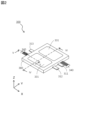
- FIG. 2 is a perspective view of the semiconductor device 300. From FIG. 2 onwards, mutually orthogonal XYZ axes are defined to clarify the correlation of the drawings.
- the upper arm 301 and the lower arm 302 of the semiconductor device 300 are arranged side by side in the Y-axis direction. Specifically, the upper arm 301 is arranged on the positive side of the Y-axis, and the lower arm 302 is arranged on the negative side of the Y-axis.
- Many components of the semiconductor device 300 are sealed with sealing resin 380. One end of the positive terminal 311, the negative terminal 312, the AC terminal 313, and the signal terminal 340 are exposed from the sealing resin 380.
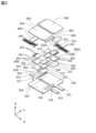
- FIG. 3 is an exploded perspective view of the semiconductor device 300.
- the sealing resin 380 that covers most of the semiconductor device 300 is not shown.
- the viewpoint of FIG. 3 is the same as that of FIG. 2.
- the semiconductor device 300 has two first conductive members 320 shown in the lower part of the figure and two second conductive members 330 shown in the upper part of the figure.
- One set of the first conductive member 320 and the second conductive member 330 is required as a component of the upper arm 301 and the lower arm 302.
- the semiconductor device 300 is a 1-in-1 device that configures only one of the upper arm 301 or the lower arm 302
- the semiconductor device 300 has only one set of the first conductive member 320 and the second conductive member 330.
- the first element 200U and the third element 210U are sandwiched between the first conductive member 320 and the second conductive member 330 that constitute the upper arm 301.
- the second element 200L and the fourth element 210L are sandwiched between the first conductive member 320 and the second conductive member 330 that constitute the lower arm 302.
- the first element 200U and the second element 200L each have a first main electrode 201, a second main electrode 202, and a signal electrode 203.
- the third element 210U and the fourth element 210L each have a third main electrode 211 and a fourth main electrode 212.
- the first main electrode 201 and the third main electrode 211 are joined to the first conductive member 320 using a first bonding material 350.
- the second main electrode 202 and the fourth main electrode 212 are joined to the second conductive member 330 using a second bonding material 351.
- the signal electrode 203 is joined to the signal terminal 340 using a third bonding material 352.
- the positive terminal 311 is connected to the first conductive member 320 constituting the upper arm 301, shown on the positive side of the Y-axis.
- the AC terminal 313 is connected to the first conductive member 320 constituting the lower arm 302, shown on the negative side of the Y-axis.
- the negative terminal 312 is disposed in a position close to the first conductive member 320 constituting the lower arm 302, and has a negative terminal connection portion 316 on the side closer to the first conductive member 320.
- the AC terminal 313 has an intermediate terminal 317.
- the intermediate terminal 317 is arranged to extend toward the upper arm 301.
- the second conductive member 330 has a terminal connection portion 332.
- the negative terminal connection portion 316 is joined to the terminal connection portion 332 of the second conductive member 330 constituting the lower arm 302 using a fourth bonding material 353.
- the intermediate terminal 317 is joined to the terminal connection portion 332 of the second conductive member 330 constituting the upper arm 301 using a fifth bonding material 354.
- the first bonding material 350, the second bonding material 351, the third bonding material 352, the fourth bonding material 353, and the fifth bonding material 354 are each a solder or a sintered material.
- the first bonding material 350, the second bonding material 351, the third bonding material 352, the fourth bonding material 353, and the fifth bonding material 354 may each have the same composition or different compositions.
- the first conductive member 320 and the second conductive member 330 may be a metal plate such as copper or aluminum, or may be an insulating substrate having a wiring layer and an insulating layer.
- the signal terminal 340 is bonded to the second conductive member 330 via the insulating heat conductive member 360.
- the insulating heat conductive member 360 is a resin with adhesive properties. This resin contains a heat conductive filler, which enhances the thermal conductivity between the signal terminal 340 and the insulating heat conductive member 360.
- the insulating heat conductive member 360 is preferably formed into a sheet shape for easy handling.
- the insulating heat conductive member 360 is bonded to the signal terminal 340 and the second conductive member 330 by applying pressure while in close contact with the signal terminal 340 and the second conductive member 330. By applying pressure to bond, voids at the adhesive interface are reduced, and insulation performance and heat dissipation performance are improved.
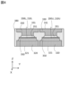
- FIG. 4 is a cross-sectional view taken along line IV-IV in FIG. 2.
- the scale in the Z-axis direction in FIG. 4 is different from that in the other figures.
- the foreground is the positive X-axis direction
- the right is the positive Y-axis direction
- the top is the positive Z-axis direction.
- the first element 200U and third element 210U constituting the upper arm 301 are arranged side by side in the X-axis direction, so they overlap when viewed from the perspective of FIG. 4.
- the second element 200L and fourth element 210L constituting the lower arm 302 are arranged side by side in the X-axis direction, so they overlap when viewed from the perspective of FIG. 4.
- the first conductive member 320 is joined to the first bonding material 350 on the positive side of the Z axis.
- the surface of the first conductive member 320 opposite the first bonding material 350 i.e., the surface on the negative side of the Z axis, is called the first heat dissipation surface 321.
- the first heat dissipation surface 321 is exposed from the sealing resin 380.
- the second conductive member 330 is joined to the second bonding material 351 on the negative side of the Z axis.
- the surface of the second conductive member 330 opposite the second bonding material 351, i.e., the surface on the positive side of the Z axis, is called the second heat dissipation surface 331.
- the second heat dissipation surface 331 is exposed from the sealing resin 380.
- the first heat dissipation surface 321 and the second heat dissipation surface 331 are thermally connected to a cooler (not shown) via an insulating member, thereby dissipating heat generated by the first element 200U, the second element 200L, the third element 210U, and the fourth element 210L.
- a cooler not shown
- an insulating thermally conductive material and a cooler may be attached to the surfaces of the first heat dissipation surface 321 and the second heat dissipation surface 331.
- an insulating thermally conductive material may be attached to the surfaces of the first heat dissipation surface 321 and the second heat dissipation surface 331, and thermally connected to the cooler via a thermally conductive material such as grease.
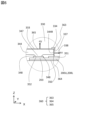
- FIG. 5 is a V-V cross-sectional view of FIG. 2.
- the right side is the positive direction of the X-axis
- the back side is the positive direction of the Y-axis
- the top is the positive direction of the Z-axis.
- the part of second conductive member 330 that protrudes in the negative direction of the Z-axis is called protrusion 338
- the configuration of second conductive member 330 excluding protrusion 338 is called base portion 330B.
- the side of protrusion 338 is called protrusion side surface 337
- the end face on the negative Z-axis side of base portion 330B is called base portion underside 333.
- the center position of protrusion 338 on the X-axis is called base center 335.
- Protrusion side surface 337 is parallel to the Z-axis.
- the second conductive member 330 has a recess 334 at the base of the protrusion 338 where the signal terminal 340 is located, and at a symmetrical position with respect to the base center 335.
- the base of the protrusion 338 is the position where the protrusion side surface 337 and the base bottom surface 333 intersect.
- the second conductive member 330 can be manufactured by various methods, but it is preferable to form the unevenness by drawing or extruding in order to improve productivity. In this case, by providing the recess 334 at a symmetrical position with the base center 335 as the center line, as described above, the force applied to the second conductive member 330 is not biased, making production easier.
- the recess 334 exists at a symmetrical position with the base center 335 as the center line.
- the recess 334 on the side where the signal terminal 340 exists is essential, but the recess 334 on the opposite side, i.e., the right side of FIG. 5, does not have to exist.
- the box shown at the bottom of FIG. 5 is an enlarged view of the end of the base 330B on the negative X-axis side.
- the insulating heat conductive member 360 is bonded to the bottom surface 333 of the base.
- the end 362 on the negative X-axis side of the insulating heat conductive member 360 is bonded to a position where it does not protrude from the conductor member side surface 336.
- the insulating heat conductive member 360 cannot be seen even if the sealing resin 380 is not present.
- the signal terminal 340 has a terminal body 344, a first bent portion 342, a second bent portion 343, a low rigidity portion 341, and a terminal portion 345.
- the terminal body 344 is bonded to the insulating heat conductive member 360.
- the second bent portion 343 is located inside the end portion 362 of the insulating heat conductive member 360, that is, on the positive side of the X-axis in FIG. 5. If the end portion 362 and the second bent portion 343 were located at the same position in the X-axis direction, it would be difficult to reliably ensure insulation, so the second bent portion 343 is located inside the end portion 362 to improve insulation performance.
- the terminal portion 345 is exposed from the sealing resin 380.
- the first bent portion 342 is located between the terminal portion 345 and the second bent portion 343.
- the first bent portion 342 is bent so that the terminal portion 345 is arranged on approximately the same plane as the positive terminal 311, the negative terminal 312, and the AC terminal 313.
- the portion to the left of the first bent portion 342 of the signal terminal 340 in the figure and inside the sealing resin 380 is referred to as the first region 340X
- the portion outside the sealing resin 380 of the signal terminal 340 is also referred to as the second region 340Y.
- the low rigidity portion 341 is located between the first bent portion 342 and the terminal portion 345.
- the low-rigidity portion 341 is sealed with sealing resin 380.
- the low-rigidity portion 341 has lower rigidity than the terminal portion 345 and the second bent portion 343.
- the terminal portion 345 When the terminal portion 345 is pressed by a mold to seal it with the sealing resin 380, the stress is received by the low-rigidity portion 341, which reduces the stress applied to the adhesive portion of the insulating thermal conductive member 360 at the second bend portion 343, thereby improving the reliability of the semiconductor device 300. Since the low-rigidity portion 341 is sealed with the sealing resin 380, the stress applied to the low-rigidity portion 341 when an external force is applied to the terminal portion 345 can be reduced, thereby improving the reliability of the semiconductor device 300.
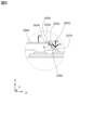
- FIG. 6 is an enlarged view of part C in FIG. 5.
- the viewpoint of FIG. 6 is the same as that of FIG. 5.
- the terminal body 344 has a protrusion 347 at a position facing the signal electrode 203.
- the protrusion 347 is joined to the signal electrode 203 using a third bonding material 352.
- Heat generated by the first element 200U and the second element 200L is transferred from the lower part to the upper part as shown in the figure as follows. That is, heat is transferred from the signal electrode 203 of the first element 200U and the second element 200L to the protrusion 347, the terminal body 344 of the signal terminal 340, the insulating heat conductive member 360, and the lower surface 333 of the base part.
- the convex portion 347 has a convex portion side surface 348.
- the convex portion side surface 348 is inclined, and is inclined so as to widen toward the base portion underside 333 side.
- the inclination of the convex portion side surface 348 makes it easier for heat to spread, improving heat dissipation.
- the shape of the convex portion 347 without using the convex portion side surface 348 can be explained as follows. That is, the convex portion 347 that protrudes into the signal electrode 203 in the signal terminal 340 has a shape that tapers toward the signal electrode 203.
- the insulating heat conductive member 360 includes a base heat transfer portion 365 extending in the X-axis direction, a side heat transfer portion 364 extending in the Z-axis direction, and a heat conductive member bent portion 363 at the corner portion.
- the heat conductive member bent portion 363 can be said to be the area sandwiched between the base heat transfer portion 365 and the side heat transfer portion 364.
- the heat conductive member bent portion 363, the side heat transfer portion 364, and the base heat transfer portion 365 are formed integrally.
- the protruding portion side surface 337 is bonded to the main body right side surface 344R using the side heat transfer portion 364. By bonding the protruding portion side surface 337 to the main body right side surface 344R, heat dissipation is improved. By butting the main body right side surface 344R against the main body right side surface 344R, the positioning of the signal terminal 340 is made easier.
- the length of the lateral heat transfer portion 364 in the Z-axis direction is set so as not to come into contact with the second bonding material 351.
- a load of ⁇ y is applied to the base heat transfer portion 365 of the insulating heat conductive member 360 in order to bond it to the base underside 333.
- a load of ⁇ x is applied to the lateral heat transfer portion 364 of the insulating heat conductive member 360 in order to bond it to the protruding portion side surface 337.
- the heat conduction member bent portion 363 Because the heat conduction member bent portion 363 is bent, it tends to be more susceptible to external forces than the lateral heat transfer portion 364 and the base heat transfer portion 365. If the heat conduction member bent portion 363 is subjected to external forces, there is a possibility that the insulation performance will deteriorate. As a countermeasure to this, the recess 334 is provided, so that the second conductive member 330 and the heat conduction member bent portion 363 do not come into contact with each other, and insulation is ensured.
- FIG. 7 is an external view of the second conductive member 330. However, FIG. 7 is taken from a different perspective than FIG. 3, and shows the surface on the negative Z-axis side that was hidden in FIG. 3.
- the protrusions 338 protruding toward the negative Z-axis side are arranged in the X-axis direction.
- the recesses 334 are present at the positive and negative X-axis ends of the protrusions 338 along the entire width of the second conductive member 330 in the Y-axis direction. Therefore, the recesses 334 can be easily processed by drawing or extruding.
- the Y-axis direction in which the recesses 334 extend is perpendicular to the X-axis direction in which the signal terminals 340 extend, making it easy to provide a flat surface on the base lower surface 333, and easy to attach to the insulating heat conductive member 360.
- the semiconductor device 300 includes a first element 200U having a first main electrode 201, a second main electrode 202, and a signal electrode 203, a sealing resin 380 that seals the first element 200U, a second conductive member 330 that protrudes from a base portion 330B that faces the first element 200U and has a protrusion 338 connected to the first main electrode 201, a signal terminal 340 having one end joined to the signal electrode 203 of the semiconductor element via a bonding material and the other end extending to the outside of the sealing resin 380, and having a terminal main body portion 344 that faces a base portion lower surface 333 that is the lower surface of the second conductive member 330, and a main body portion right side surface 344R that faces a protrusion portion side surface 337 that is the side surface of the protrusion 338, and an insulating thermally conductive member 360 that is arranged between the second conductive member 330 and the signal terminal
- the second conductive member 330 and the signal terminal 340 have a recess 334 between the base lower surface 333 and the protrusion 338. This improves heat dissipation performance and insulation.
- the signal electrode 203 and the signal terminal 340 are thermally connected to the second conductive member 330 via the insulating thermal conductive member 360. Heat is dissipated from the signal terminal 340 to the second conductive member 330, and a heat dissipation path is provided, thereby improving heat dissipation performance.
- the insulation is improved by providing the recess 334 at the point where the insulating thermal conductive member 360 is bent.
- the signal terminal 340 has a first region 340X sealed in the sealing resin 380 and a second region 340Y extending outside the sealing resin 380.
- the first region 340X of the signal terminal 340 has a low-rigidity portion 341 formed therein that has a lower rigidity than other portions of the first region 340X. Therefore, when sealing is performed using the sealing resin 380, stress is not easily applied to the adhesive interface between the insulating thermal conductive member 360 and the signal terminal 340, which makes it possible to suppress peeling and improves productivity.
- the insulating heat conductive member 360 is disposed within the range of the second conductive member 330 when viewed in the direction in which the protrusion 338 protrudes, i.e., the Z-axis direction. This prevents the insulating heat conductive member 360 from cracking during the manufacture of the semiconductor device 300, improving the productivity of the semiconductor device 300.
- the second conductive member 330 has a terminal portion 345 that extends outside the sealing resin 380.
- the terminal portion 345 is disposed on the same plane as the second region 340Y. This simplifies the mold for the sealing resin 380, improving the productivity of the semiconductor device 300.
- the recess 334 is formed symmetrically with respect to the protrusion 338. This makes it easier to press-form the recess 334, improving the productivity of the semiconductor device 300.
- the recess 334 extends in a direction perpendicular to the extension direction of the signal terminal 340. Therefore, the recess 334 can be formed by extrusion molding or drawing shaping, improving the productivity of the semiconductor device 300.
- the terminal body 344 has a protrusion 347 that faces the signal electrode 203, and the protrusion 347 is inclined so as to extend from the signal electrode 203 to the terminal body 344. This improves heat dissipation.
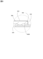
- FIG. 8 is an enlarged view of the C portion in the first modification.
- FIG. 8 corresponds to FIG. 6 in the embodiment.
- the right side surface 344R of the main body and the side surface 337 of the protruding portion are inclined.
- the right side surface 344R of the main body and the side surface 337 of the protruding portion are parallel to the Z axis, but in this modification, the right side surface 344R of the main body and the side surface 337 of the protruding portion are not parallel to the Z axis.
- the side surface 337 of the protruding portion is inclined, when a load of ⁇ 0 is applied, a load ⁇ 1 for bonding the insulating heat conductive member 360 can also be generated on the side surface 337A of the protruding portion, improving productivity. It is preferable that the inclination angle ⁇ is 135° or more. If the inclination angle ⁇ is large, ⁇ 1 increases, and bonding of the insulating heat conductive member 360 becomes easier.
- the recess 334A in this modified example has a recess side 392A.
- the recess side 392A is inclined. The inclination allows for easy processing during drawing and extrusion, improving productivity.
- the rest of the shape is the same as in the embodiment.
- the side surface of the main body is inclined from the main body toward the main electrode, which allows heat from the signal electrode 203 to spread more easily, improving heat dissipation performance.
- the angle of the side of the main body relative to the main body is 135 degrees or more. This increases the load for bonding the insulating heat conductive member 360, making it easier to bond the insulating heat conductive member 360.
- FIG. 9 is an enlarged view of the C portion in the second modified example.
- FIG. 9 corresponds to FIG. 6 in the embodiment.
- the recess 334 is provided at the intersection of the protrusion 338 and the base lower surface 333.
- the terminal body 344 has the terminal recess 346B.
- the terminal recess 346B is disposed at a position where the thermal conductive member bent portion 363 avoids the terminal body 344. That is, the terminal recess 346B is provided on the opposite side of the thermal conductive member bent portion 363 from the recess 334. Therefore, by providing the terminal recess 346B instead of the recess 334, the insulation performance can be improved as in the embodiment.
- the other structures are the same as in the embodiment.
- semiconductor device 300 may have at least one of recess 334 and terminal recess 346B. In other words, semiconductor device 300 may have both recess 334 and terminal recess 346B.
- (Variation 3) 10 is a diagram showing a power conversion device 1 in Modification 3.
- the power conversion device 1 includes three semiconductor devices 300, a group of film capacitors 3G for voltage conversion, and a control board 7. This is a circuit diagram of the power conversion device 1.
- the power conversion device 1 converts DC power and AC power mutually.
- the power conversion device 1 may convert DC power provided from a high-voltage battery 2 into AC power and supply it to a motor generator MG, or may convert AC power provided from the motor generator MG into DC power and supply it to the high-voltage battery 2.
- the high-voltage battery 2 is a secondary battery such as a lithium-ion battery or a nickel-metal hydride battery.
- the motor generator MG uses AC power to output driving force for the HEV or EV.
- the motor generator MG also acts as a generator that regenerates AC power to the high-voltage battery 2 when the motor is rotated by an external force.
- the motor generator MG is, for example, a three-phase motor with a Y connection as shown in Figure 1.
- the film capacitor group 3G is a modularization of multiple film capacitors 3 arranged in a resin case and sealed with resin.
- the film capacitor group 3G performs smoothing when converting DC power to AC power.
- Each semiconductor device 300 converts the DC power of the high-voltage battery 2 into three-phase AC power by controlling the on and off timing of the switching elements that make up the U-phase arm, V-phase arm, and W-phase arm.
- the control board 7 is equipped with a microcomputer that performs arithmetic processing. The control board 7 creates gate pulse signals based on input information from the upper controller 10 and outputs them to each semiconductor device 300.
- the power conversion device 1 includes the semiconductor device 300 and a control board 7 that controls the semiconductor device 300. Therefore, it is possible to provide the power conversion device 1 that includes the semiconductor device 300 that has excellent heat dissipation and insulation properties. Note that the power conversion device 1 may include only one semiconductor device 300 and be compatible with a single phase.
Landscapes
- Cooling Or The Like Of Semiconductors Or Solid State Devices (AREA)
Abstract
Description
本発明の第2の態様による電力変換装置は、上述した半導体装置と、入力される電力を変換して出力する主変換回路とを備える。
以下、図1~図7を参照して、半導体装置の実施の形態を説明する。
(1)半導体装置300は、第1主電極201、第2主電極202、および信号電極203を有する第1素子200Uと、第1素子200Uを封止する封止樹脂380と、第1素子200Uと対向するベース部330Bから突出し、第1主電極201に接続された突出部338を有する第2導電部材330と、一端が半導体素子の信号電極203に接合材を介して接合されており、他端が封止樹脂380の外部まで延び、第2導電部材330の下面であるベース部下面333と対向する端子本体部344、および突出部338の側面である突出部側面337と対向する本体部右側面344R、を有する信号端子340と、第2導電部材330と信号端子340との間に配置された絶縁性熱伝導部材360と、を備える。第2導電部材330と信号端子340は、ベース部下面333と突出部338との間に凹部334を備える。そのため、放熱性能および絶縁性を向上できる。具体的には、信号電極203と信号端子340とが絶縁性熱伝導部材360を介して第2導電部材330に熱的に接続される。信号端子340から第2導電部材330に放熱し、放熱経路を設けることで放熱性が向上する。また、絶縁性熱伝導部材360が屈曲する箇所に凹部334が設けられることで、絶縁性が向上される。
図8は、変形例1におけるC部の拡大図である。図8は、実施の形態における図6に対応する。変形例1では、本体部右側面344Rおよび突出部側面337が斜面になっている。換言すると、上述した実施の形態では、本体部右側面344Rおよび突出部側面337はZ軸に平行であったが、本変形例における本体部右側面344Rおよび突出部側面337はZ軸と平行ではない。本変形例では突出部側面337が傾斜なので、σ0の荷重を印加すると突出部側面337Aにも絶縁性熱伝導部材360を接着する荷重σ1を発生させることができ生産性が向上する。傾斜角度θは135°以上あることが好ましい。傾斜角度θが大きければ、σ1が増え、絶縁性熱伝導部材360の接着が容易になる。
(8)本体部側面は、本体部から主電極に近づくように傾斜している。そのため、信号電極203からの熱が広がりやすくなり放熱性能が向上する。
図9は、変形例2におけるC部の拡大図である。図9は、実施の形態における図6に対応する。上述した実施の形態では、突出部338とベース部下面333の交点に凹部334を有していた。しかし本変形例では端子本体部344が端子凹部346Bを有する。端子凹部346Bは、熱伝導部材屈曲部363が端子本体部344を避ける位置に配置される。すなわち、端子凹部346Bは熱伝導部材屈曲部363を挟んで凹部334と逆側に設けられる。そのため、凹部334の代わりに端子凹部346Bが設けられることで、実施の形態と同様に絶縁性能を向上することができる。その他の構造は、実施の形態と同様である。
図10は、変形例3における電力変換装置1を示す図である。電力変換装置1は、3つの半導体装置300と、電圧変換用のフィルムコンデンサ群3Gと、制御基板7とを備える。電力変換装置1の回路図である。電力変換装置1は、直流電力と交流電力とを相互に変換する。電力変換装置1は、高電圧バッテリー2から提供される直流電力を交流電力に変換してモータジェネレータMGに供給する場合と、モータジェネレータMGから提供される交流電力を直流電力に変換して高電圧バッテリー2に供給する場合とがある。高電圧バッテリー2は、リチウムイオン電池やニッケル水素電池などの2次電池である。
(10)電力変換装置1は、半導体装置300と、半導体装置300を制御する制御基板7とを備える。そのため、放熱性能および絶縁性に優れる半導体装置300を内蔵する電力変換装置1を提供できる。なお、電力変換装置1は半導体装置300を1つのみ備え、単相に対応してもよい。
Claims (10)
- 主電極および信号電極を有する半導体素子と、
前記半導体素子を封止する封止樹脂と、
前記半導体素子と対向する下面から突出し、前記主電極に接続された突出部を有する導電部材と、
一端が前記半導体素子の前記信号電極に接合材を介して接合されており、他端が前記封止樹脂の外部まで延び、前記導電部材の下面と対向する本体部、および前記突出部の側面と対向する本体部側面、を有する信号端子と、
前記導電部材と前記信号端子との間に配置された絶縁性熱伝導部材と、
を備え、
前記導電部材と前記信号端子は、前記導電部材の下面と前記突出部との間、および前記本体部と前記本体部側面との間の少なくとも一方に凹部を備える、半導体装置。 - 請求項1に記載の半導体装置において、
前記信号端子は、前記封止樹脂に封止されている第1領域と、前記封止樹脂の外側に延伸する第2領域と、を有し、
前記第1領域は、前記第1領域の他の部分よりも剛性が低い低剛性部が形成されている、半導体装置。 - 請求項1に記載の半導体装置において、
前記絶縁性熱伝導部材は、前記突出部が突出する方向から見たとき、前記導電部材の範囲内に配置されている、半導体装置。 - 請求項2に記載の半導体装置において、
前記導電部材は、封止樹脂の外側に延伸した主端子部を有し、
前記主端子部は、前記第2領域と同一平面上に配置されている、半導体装置。 - 請求項1に記載の半導体装置において、
前記凹部は、前記突出部に対して対称に形成されている、半導体装置。 - 請求項1に記載の半導体装置において、
前記凹部は、前記信号端子の延伸方向に対して垂直な方向に向かって伸びる、半導体装置。 - 請求項1に記載の半導体装置において、
前記本体部は、前記信号電極に向かう凸部を有し、
前記凸部は、前記信号電極から前記本体部に広がるような傾斜が設けられている、半導体装置。 - 請求項1に記載の半導体装置において、
前記本体部側面は、前記本体部から前記主電極に近づくように傾斜している、半導体装置。 - 請求項1に記載の半導体装置において、
前記本体部側面の前記本体部に対しての角度は、135度以上である、半導体装置。 - 請求項1に記載の半導体装置と、入力される電力を変換して出力する主変換回路とを備える電力変換装置。
Priority Applications (4)
| Application Number | Priority Date | Filing Date | Title |
|---|---|---|---|
| JP2024572790A JPWO2024157458A1 (ja) | 2023-01-27 | 2023-01-27 | |
| CN202380089572.9A CN120457541A (zh) | 2023-01-27 | 2023-01-27 | 半导体装置、电力变换装置 |
| PCT/JP2023/002659 WO2024157458A1 (ja) | 2023-01-27 | 2023-01-27 | 半導体装置、電力変換装置 |
| DE112023004544.5T DE112023004544T5 (de) | 2023-01-27 | 2023-01-27 | Halbleitervorrichtung und leistungsumsetzungsvorrichtung |
Applications Claiming Priority (1)
| Application Number | Priority Date | Filing Date | Title |
|---|---|---|---|
| PCT/JP2023/002659 WO2024157458A1 (ja) | 2023-01-27 | 2023-01-27 | 半導体装置、電力変換装置 |
Publications (1)
| Publication Number | Publication Date |
|---|---|
| WO2024157458A1 true WO2024157458A1 (ja) | 2024-08-02 |
Family
ID=91970111
Family Applications (1)
| Application Number | Title | Priority Date | Filing Date |
|---|---|---|---|
| PCT/JP2023/002659 Ceased WO2024157458A1 (ja) | 2023-01-27 | 2023-01-27 | 半導体装置、電力変換装置 |
Country Status (4)
| Country | Link |
|---|---|
| JP (1) | JPWO2024157458A1 (ja) |
| CN (1) | CN120457541A (ja) |
| DE (1) | DE112023004544T5 (ja) |
| WO (1) | WO2024157458A1 (ja) |
Citations (5)
| Publication number | Priority date | Publication date | Assignee | Title |
|---|---|---|---|---|
| WO2018179981A1 (ja) * | 2017-03-29 | 2018-10-04 | トヨタ自動車株式会社 | 半導体装置 |
| JP2018164050A (ja) * | 2017-03-27 | 2018-10-18 | トヨタ自動車株式会社 | 半導体モジュール |
| JP2020096085A (ja) * | 2018-12-12 | 2020-06-18 | トヨタ自動車株式会社 | 半導体装置 |
| JP2020113582A (ja) * | 2019-01-08 | 2020-07-27 | トヨタ自動車株式会社 | 半導体装置 |
| JP2020167287A (ja) * | 2019-03-29 | 2020-10-08 | 株式会社デンソー | 半導体装置 |
-
2023
- 2023-01-27 JP JP2024572790A patent/JPWO2024157458A1/ja active Pending
- 2023-01-27 WO PCT/JP2023/002659 patent/WO2024157458A1/ja not_active Ceased
- 2023-01-27 DE DE112023004544.5T patent/DE112023004544T5/de active Pending
- 2023-01-27 CN CN202380089572.9A patent/CN120457541A/zh active Pending
Patent Citations (5)
| Publication number | Priority date | Publication date | Assignee | Title |
|---|---|---|---|---|
| JP2018164050A (ja) * | 2017-03-27 | 2018-10-18 | トヨタ自動車株式会社 | 半導体モジュール |
| WO2018179981A1 (ja) * | 2017-03-29 | 2018-10-04 | トヨタ自動車株式会社 | 半導体装置 |
| JP2020096085A (ja) * | 2018-12-12 | 2020-06-18 | トヨタ自動車株式会社 | 半導体装置 |
| JP2020113582A (ja) * | 2019-01-08 | 2020-07-27 | トヨタ自動車株式会社 | 半導体装置 |
| JP2020167287A (ja) * | 2019-03-29 | 2020-10-08 | 株式会社デンソー | 半導体装置 |
Also Published As
| Publication number | Publication date |
|---|---|
| JPWO2024157458A1 (ja) | 2024-08-02 |
| DE112023004544T5 (de) | 2025-08-21 |
| CN120457541A (zh) | 2025-08-08 |
Similar Documents
| Publication | Publication Date | Title |
|---|---|---|
| JP5067267B2 (ja) | 樹脂封止型半導体装置とその製造方法 | |
| US10026673B2 (en) | Semiconductor device and power module | |
| US10366957B2 (en) | Semiconductor device | |
| JP7491707B2 (ja) | 電気回路体、電力変換装置、および電気回路体の製造方法 | |
| US20160126157A1 (en) | Double-sided cooling power module and method for manufacturing the same | |
| US10720383B2 (en) | Semiconductor device configuring upper and lower arms including auxiliary terminals | |
| WO2017199723A1 (ja) | 半導体装置 | |
| US11996344B2 (en) | Semiconductor device | |
| JP4973059B2 (ja) | 半導体装置及び電力変換装置 | |
| JP6575739B1 (ja) | 半導体装置、半導体装置の製造方法および電力変換装置 | |
| JP7363587B2 (ja) | 半導体装置 | |
| WO2023149144A1 (ja) | 半導体装置 | |
| JP7268563B2 (ja) | 半導体装置 | |
| WO2016203743A1 (ja) | 半導体装置 | |
| JP7693094B2 (ja) | パワーモジュール半導体パッケージおよび半導体装置 | |
| JP2021141171A (ja) | 半導体装置 | |
| WO2023022001A1 (ja) | パワーモジュールおよび電力変換装置 | |
| US20240297100A1 (en) | Semiconductor module, semiconductor device, and vehicle | |
| CN120457541A (zh) | 半导体装置、电力变换装置 | |
| JP7428679B2 (ja) | パワー半導体装置および電力変換装置 | |
| US20250379138A1 (en) | Semiconductor device | |
| JP2020113600A (ja) | 半導体装置 | |
| JP2025171942A (ja) | 半導体装置 | |
| WO2025234243A1 (ja) | 半導体装置 | |
| WO2026018651A1 (ja) | 半導体装置 |
Legal Events
| Date | Code | Title | Description |
|---|---|---|---|
| 121 | Ep: the epo has been informed by wipo that ep was designated in this application |
Ref document number: 23918420 Country of ref document: EP Kind code of ref document: A1 |
|
| WWE | Wipo information: entry into national phase |
Ref document number: 2024572790 Country of ref document: JP Ref document number: 202380089572.9 Country of ref document: CN |
|
| WWE | Wipo information: entry into national phase |
Ref document number: 112023004544 Country of ref document: DE |
|
| WWP | Wipo information: published in national office |
Ref document number: 202380089572.9 Country of ref document: CN |
|
| WWP | Wipo information: published in national office |
Ref document number: 112023004544 Country of ref document: DE |
|
| 122 | Ep: pct application non-entry in european phase |
Ref document number: 23918420 Country of ref document: EP Kind code of ref document: A1 |