WO2024154438A1 - 撮像装置およびカメラシステム - Google Patents
撮像装置およびカメラシステム Download PDFInfo
- Publication number
- WO2024154438A1 WO2024154438A1 PCT/JP2023/042399 JP2023042399W WO2024154438A1 WO 2024154438 A1 WO2024154438 A1 WO 2024154438A1 JP 2023042399 W JP2023042399 W JP 2023042399W WO 2024154438 A1 WO2024154438 A1 WO 2024154438A1
- Authority
- WO
- WIPO (PCT)
- Prior art keywords
- photoelectric conversion
- current
- imaging device
- electrode
- circuit
- Prior art date
- Legal status (The legal status is an assumption and is not a legal conclusion. Google has not performed a legal analysis and makes no representation as to the accuracy of the status listed.)
- Ceased
Links
Images


Classifications
-
- H—ELECTRICITY
- H04—ELECTRIC COMMUNICATION TECHNIQUE
- H04N—PICTORIAL COMMUNICATION, e.g. TELEVISION
- H04N23/00—Cameras or camera modules comprising electronic image sensors; Control thereof
- H04N23/60—Control of cameras or camera modules
- H04N23/667—Camera operation mode switching, e.g. between still and video, sport and normal or high- and low-resolution modes
-
- H—ELECTRICITY
- H04—ELECTRIC COMMUNICATION TECHNIQUE
- H04N—PICTORIAL COMMUNICATION, e.g. TELEVISION
- H04N25/00—Circuitry of solid-state image sensors [SSIS]; Control thereof
- H04N25/50—Control of the SSIS exposure
- H04N25/53—Control of the integration time
- H04N25/532—Control of the integration time by controlling global shutters in CMOS SSIS
-
- H—ELECTRICITY
- H04—ELECTRIC COMMUNICATION TECHNIQUE
- H04N—PICTORIAL COMMUNICATION, e.g. TELEVISION
- H04N25/00—Circuitry of solid-state image sensors [SSIS]; Control thereof
- H04N25/70—SSIS architectures; Circuits associated therewith
-
- H—ELECTRICITY
- H04—ELECTRIC COMMUNICATION TECHNIQUE
- H04N—PICTORIAL COMMUNICATION, e.g. TELEVISION
- H04N25/00—Circuitry of solid-state image sensors [SSIS]; Control thereof
- H04N25/70—SSIS architectures; Circuits associated therewith
- H04N25/709—Circuitry for control of the power supply
-
- H—ELECTRICITY
- H04—ELECTRIC COMMUNICATION TECHNIQUE
- H04N—PICTORIAL COMMUNICATION, e.g. TELEVISION
- H04N25/00—Circuitry of solid-state image sensors [SSIS]; Control thereof
- H04N25/70—SSIS architectures; Circuits associated therewith
- H04N25/76—Addressed sensors, e.g. MOS or CMOS sensors
-
- H—ELECTRICITY
- H04—ELECTRIC COMMUNICATION TECHNIQUE
- H04N—PICTORIAL COMMUNICATION, e.g. TELEVISION
- H04N25/00—Circuitry of solid-state image sensors [SSIS]; Control thereof
- H04N25/70—SSIS architectures; Circuits associated therewith
- H04N25/76—Addressed sensors, e.g. MOS or CMOS sensors
- H04N25/77—Pixel circuitry, e.g. memories, A/D converters, pixel amplifiers, shared circuits or shared components
-
- H—ELECTRICITY
- H04—ELECTRIC COMMUNICATION TECHNIQUE
- H04N—PICTORIAL COMMUNICATION, e.g. TELEVISION
- H04N23/00—Cameras or camera modules comprising electronic image sensors; Control thereof
- H04N23/20—Cameras or camera modules comprising electronic image sensors; Control thereof for generating image signals from infrared radiation only
- H04N23/21—Cameras or camera modules comprising electronic image sensors; Control thereof for generating image signals from infrared radiation only from near infrared [NIR] radiation
-
- H—ELECTRICITY
- H04—ELECTRIC COMMUNICATION TECHNIQUE
- H04N—PICTORIAL COMMUNICATION, e.g. TELEVISION
- H04N23/00—Cameras or camera modules comprising electronic image sensors; Control thereof
- H04N23/56—Cameras or camera modules comprising electronic image sensors; Control thereof provided with illuminating means
Definitions
- This disclosure relates to an imaging device and a camera system.
- CMOS Complementary Metal Oxide Semiconductor
- CMOS type image sensors with photodiodes are widely used as image sensors.
- CMOS type image sensors have the advantages of low power consumption and the ability to access each pixel.
- CMOS type image sensors generally use the so-called rolling shutter method as a signal readout method, in which exposure and signal charge are read out sequentially for each row of the pixel array.
- the start and end of exposure is different for each row of the pixel array.
- a distorted image of the object may be obtained, and when a flash is used, differences in brightness may occur within the image.
- Patent Document 1 discloses a method for achieving a global shutter function in an image sensor with a stacked structure in which the circuit section and the photoelectric conversion section are separated, by changing the voltage supplied to the photoelectric conversion section, thereby controlling the movement of signal charge from the photoelectric conversion section to the charge accumulation region.
- Patent Document 2 also proposes an asynchronous solid-state imaging device called an event-driven sensor and dynamic vision sensor, which detects an event for each pixel when the amount of received light exceeds a threshold.
- This disclosure provides an imaging device and a camera system that can detect changes in a subject.
- a camera system includes the imaging device described above and an illumination device that emits light including near-infrared rays.
- This disclosure provides an imaging device and camera system that can detect changes in a subject.
- FIG. 1 is a block diagram illustrating an example of a camera system according to an embodiment.
- FIG. 2 is a schematic diagram illustrating an exemplary circuit configuration of the image sensor according to the embodiment.
- FIG. 3 is a cross-sectional view illustrating a schematic example of a device structure of a pixel according to an embodiment.
- FIG. 4 is a plan view showing an example of a planar layout of pixel electrodes and shield electrodes according to the embodiment.
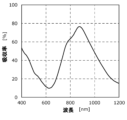
- FIG. 5 is a diagram showing an example of an absorption spectrum in a photoelectric conversion layer containing tin phthalocyanine.
- FIG. 6 is a cross-sectional view illustrating an example of a configuration of a photoelectric conversion layer according to an embodiment.
- FIG. 1 is a block diagram illustrating an example of a camera system according to an embodiment.
- FIG. 2 is a schematic diagram illustrating an exemplary circuit configuration of the image sensor according to the embodiment.
- FIG. 3 is a cross-sectional view illustrating a schematic example of
- FIG. 7 is a diagram showing exemplary photocurrent characteristics of a photoelectric conversion unit according to the embodiment.
- FIG. 8 is a diagram for explaining an example of the operation of the normal imaging drive in the imaging device according to the embodiment.
- FIG. 9 is a schematic diagram for explaining the arrangement of a current measuring circuit according to an embodiment.
- FIG. 10A is a diagram for explaining an example of the operation and output result of the current change detection drive in the imaging device according to the embodiment.
- FIG. 10B is a diagram for explaining an example of the operation and output result of the current change detection drive in the imaging device according to the embodiment.
- FIG. 11 is a diagram for explaining a first example of control of the drive mode in the imaging device according to the embodiment.
- FIG. 12 is a diagram for explaining a second example of control of the drive mode in the imaging device according to the embodiment.
- FIG. 13 is a diagram for explaining a third example of control of the drive mode in the imaging device according to the embodiment.
- the imaging device includes a photoelectric conversion unit including a first electrode, a second electrode facing the first electrode, and a photoelectric conversion layer located between the first electrode and the second electrode, a first voltage supply circuit that applies a voltage between the first electrode and the second electrode, a signal detection circuit that detects a signal based on charges generated in the photoelectric conversion unit, at least one current measurement circuit that measures a current flowing in the photoelectric conversion unit, and a current change detection circuit that detects a change in the current flowing in the photoelectric conversion unit measured by the at least one current measurement circuit.
- the current change detection circuit detects the change in the current flowing through the photoelectric conversion unit measured by the current measurement circuit, thereby making it possible to detect changes in the subject.
- an imaging device may be the imaging device according to the first aspect, further comprising a charge storage unit connected to the first electrode and storing the charge generated by the photoelectric conversion unit.
- the first voltage supply circuit may apply the voltage between the first electrode and the second electrode by supplying a predetermined voltage to the second electrode, and the at least one current measurement circuit may include a first current measurement circuit connected to the second electrode.
- an imaging device is an imaging device according to the second aspect, in which the second electrode may be divided into a plurality of sub-second electrodes, the at least one current measurement circuit may include a plurality of current measurement circuits, the plurality of current measurement circuits may be a plurality of the first current measurement circuits, and each of the plurality of sub-second electrodes may be connected to a corresponding first current measurement circuit of the plurality of first current measurement circuits.
- an imaging device may be an imaging device according to any one of the first to fifth aspects, further comprising a charge storage section connected to the first electrode and storing the charge generated by the photoelectric conversion section, and a second voltage supply circuit supplying a predetermined voltage to the charge storage section.
- the at least one current measurement circuit may include at least one third current measurement circuit connected to the second voltage supply circuit.
- the imaging device may be the imaging device according to the sixth aspect, further comprising a plurality of pixels, each of which may include the photoelectric conversion unit, the signal detection circuit, and the charge storage unit.
- the at least one third current measurement circuit may include a plurality of the third current measurement circuits.
- the plurality of pixels may include a first pixel and a second pixel different from the first pixel.
- a corresponding third current measurement circuit among the plurality of third current measurement circuits may be located at a location of a first wiring path connecting the charge storage unit included in the first pixel and the second voltage supply circuit that does not overlap with a second wiring path connecting the charge storage unit included in the second pixel and the second voltage supply circuit, and at a location of the second wiring path that does not overlap with the first wiring path.
- an imaging device may be an imaging device according to any one of the first to seventh aspects, and the at least one current measurement circuit may include multiple current measurement circuits.
- an imaging device is an imaging device according to any one of the first to eighth aspects, and may further include a plurality of pixels, each of which may include the photoelectric conversion unit and the signal detection circuit.
- the number of the at least one current measurement circuit may be less than the number of the plurality of pixels.
- an imaging device may be an imaging device according to any one of the first to ninth aspects, further including a drive control circuit that controls driving of the imaging device.
- the drive control circuit may control the imaging device to perform (i) a current change detection drive in which the current change detection circuit detects the change in the current flowing in the photoelectric conversion unit, and (ii) a normal imaging drive in which the signal detection circuit detects the signal based on the charge generated in the photoelectric conversion unit.
- the imaging device can detect changes in the subject using current change detection drive, while in normal imaging drive it can detect signals for image generation based on the charge generated in the photoelectric conversion unit, and output detailed images.
- an imaging device is the imaging device according to the tenth aspect, and the drive control circuit may switch the drive of the imaging device from the current change detection drive to the normal imaging drive when the current change detection circuit detects the change in the current flowing in the photoelectric conversion unit while the imaging device is performing the current change detection drive.
- an imaging device may be the imaging device according to the eleventh aspect, and the drive control circuit may switch the drive of the imaging device from the normal imaging drive to the current change detection drive after a predetermined time has elapsed since the imaging device started the normal imaging drive.
- an imaging device is an imaging device according to any one of the tenth to twelfth aspects, and the drive control circuit may set at least some of the signal detection circuit and the circuits connected to the signal detection circuit in an off state or standby state while the drive control circuit controls the imaging device to perform the current change detection drive.
- an imaging device may be the imaging device according to the tenth aspect, and the drive control circuit may control the imaging device to perform the current change detection drive and the normal imaging drive simultaneously.
- a camera system includes an imaging device according to any one of the first to fourteenth aspects and an illumination device that emits light including near-infrared rays.
- the terms “above” and “below” do not refer to the upward (vertically upward) and downward (vertically downward) directions in absolute spatial recognition, but are used as terms defined by a relative positional relationship based on the stacking order in the stacked configuration.
- the light receiving side of the imaging device is referred to as “above” and the side opposite the light receiving side is referred to as “below”.
- “above” and “below” are used only to specify the relative arrangement of components, and are not intended to limit the position of the imaging device when in use.
- the terms “above” and “below” are applied not only to cases where two components are arranged with a gap between them and another component is present between the two components, but also to cases where two components are arranged closely together and are in contact with each other.
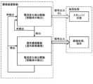
- FIG. 1 is a block diagram showing an example of a camera system 1 according to the present embodiment.
- the camera system 1 includes an imaging device 100, an illumination device 200, an image processing unit 300, and a system controller 400.
- camera system 1 ambient light and illumination light emitted by lighting device 200 are reflected by the subject, and the reflected light is converted into an electric charge by the photoelectric conversion unit of imaging device 100, and is extracted as an electrical signal and imaged.
- ambient light such as sunlight or external lighting is used for imaging
- camera system 1 does not need to be equipped with lighting device 200.
- the imaging device 100 includes an imaging element 110, a current change detection circuit 130, and a drive control circuit 140.
- the imaging element 110 has a photoelectric conversion unit 13, and outputs a signal based on light incident on the photoelectric conversion unit 13.
- the imaging element 110 also has a current measurement circuit 19 connected to the photoelectric conversion unit 13.
- the current measurement circuit 19 measures the current flowing in the photoelectric conversion unit 13. Note that at least some of the circuit elements of the current measurement circuit 19 may be provided outside the imaging element 110.
- the current change detection circuit 130 detects the change in the current measured by the current measurement circuit 19.
- the current change detection circuit 130 can detect the presence of a moving object, for example, based on the detected change in current.
- the drive control circuit 140 controls the operation of the imaging device 100 (mainly the imaging element 110).
- the current change detection circuit 130 and the drive control circuit 140 are each realized by one or more microcomputers or processors that incorporate programs for performing processing in the current change detection circuit 130 and the drive control circuit 140.
- the current change detection circuit 130 and the drive control circuit 140 may also be realized by individual microcomputers or processors, or may be realized by a single microcomputer or processor.
- the current change detection circuit 130 and the drive control circuit 140 may each include a dedicated logic circuit for performing processing in the current change detection circuit 130 and the drive control circuit 140. Details of the imaging device 100 will be described later.
- the lighting device 200 irradiates light containing, for example, near-infrared light as the lighting light.
- an electrical signal generated by photoelectric conversion in a photoelectric conversion section of the imaging device 100 that is sensitive to near-infrared wavelengths is extracted and imaged.
- the wavelength range of the near-infrared light contained in the lighting light is, for example, 680 nm or more and 3000 nm or less.
- the wavelength range of the near-infrared light contained in the lighting light may be 700 nm or more and 2000 nm or less, or 700 nm or more and 1600 nm or less.
- the lighting light does not have to contain near-infrared light, and may contain at least one of visible light and ultraviolet light.
- the type of light source used in the lighting device 200 is not particularly limited as long as it is a light source that can emit light of the desired wavelength.
- the light source used in the lighting device 200 is, for example, a halogen light source, an LED (Light Emitting Diode) light source, an organic EL (Electro Luminescence) light source, or a laser diode light source.
- the light source used in the lighting device 200 may be a combination of multiple light sources with different emission wavelengths.
- an inexpensive LED with a peak wavelength of 820 nm or more and 980 nm or less can be used as a light source that emits light including near-infrared rays.
- the image processing unit 300 is a processing circuit that performs various processes on output signals including image data output from the imaging device 100.
- the image processing unit 300 performs processes such as gamma correction, color interpolation, spatial interpolation, auto white balance, distance measurement calculation, and wavelength information separation.
- the image processing unit 300 processes the output signal from the imaging device 100 and outputs it to the outside as an image.
- the image processing unit 300 is realized by one or more microcomputers or processors that incorporate a program for performing the processing in the image processing unit 300.
- the image processing unit 300 may include a dedicated logic circuit for performing the processing in the image processing unit 300.
- a specific example of the image processing unit 300 is an ISP (Image Signal Processor).
- the system controller 400 controls the entire camera system 1. For example, the system controller 400 controls the timing of image capture by the image capture device 100 and the timing of illumination light irradiation by the illumination device 200.
- the system controller 400 is realized by one or more microcomputers or processors that incorporate a program for performing processing in the system controller 400.
- the system controller 400 may include a dedicated logic circuit for performing processing in the system controller 400.
- the imaging device 100, the lighting device 200, the image processing unit 300, and the system controller 400 are shown as separate functional blocks, but two or more of the imaging device 100, the lighting device 200, the image processing unit 300, and the system controller 400 may be integrated together by being provided in the same housing, etc. Also, the image processing unit 300 and the system controller 400 may each be realized by separate microcomputers or processors, etc., or may be realized by a single microcomputer or processor, etc.
- the functions of the image processing unit 300 and the system controller 400 may be possessed by the imaging device 100.
- at least one of the image processing unit 300 and the system controller 400 may be provided in the imaging device 100.
- the current change detection circuit 130, the drive control circuit 140, the image processing unit 300, and the system controller 400 may each be realized by an individual microcomputer or processor, etc., and two or more of these functions may be realized by a single microcomputer or processor, etc.
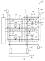
- FIG. 2 is a schematic diagram showing an exemplary circuit configuration of the image sensor 110 according to this embodiment. Note that the current measurement circuit 19 is omitted from FIG. 2. First, the configuration for capturing a normal image in the image sensor 110 will be described. Details of the current measurement circuit 19 will be described later.
- the imaging element 110 has a pixel array PA including a plurality of pixels 10 arranged two-dimensionally, and peripheral circuits having connections to each pixel 10.
- the peripheral circuits include, for example, a shield voltage supply circuit 18, a voltage supply circuit 32, a reset voltage source 34, a vertical scanning circuit 36, a column signal processing circuit 37, and a horizontal signal readout circuit 38.
- FIG. 2 shows a schematic example in which the pixels 10 are arranged in a matrix of two rows and two columns. The number and arrangement of the pixels 10 in the imaging element 110 are not limited to the example shown in FIG. 2.
- Each pixel 10 has a photoelectric conversion unit 13 and a signal detection circuit 14.
- the photoelectric conversion unit 13 has a photoelectric conversion layer sandwiched between two opposing electrodes, and receives incident light to generate a signal charge.
- the photoelectric conversion unit 13 does not need to be an independent element for each pixel 10 in its entirety, and for example, a portion of the photoelectric conversion unit 13 may span multiple pixels 10.
- the signal detection circuit 14 is a circuit that detects a pixel signal, which is an example of a signal based on the charge generated by the photoelectric conversion unit 13.
- the signal detection circuit 14 includes a signal detection transistor 24 and an address transistor 26.
- the signal detection transistor 24 and the address transistor 26 are, for example, field effect transistors (FETs), and here, an N-channel MOSFET (Metal Oxide Semiconductor Field Effect Transistor) is exemplified as the signal detection transistor 24 and the address transistor 26.
- Each transistor, such as the signal detection transistor 24, the address transistor 26, and the reset transistor 28 described later, has a control terminal, an input terminal, and an output terminal.
- the control terminal is, for example, a gate.
- the input terminal is one of the drain and the source, for example, the drain.
- the output terminal is the other of the drain and the source, for example, the source.
- the control terminal of the signal detection transistor 24 has an electrical connection with the photoelectric conversion unit 13.
- the signal charge generated by the photoelectric conversion unit 13 is stored in a charge storage region including a charge storage node 41 between the gate of the signal detection transistor 24 and the photoelectric conversion unit 13.
- the signal charge is holes and electrons.
- the charge storage node 41 is also called a "floating diffusion node.”
- the charge storage node 41 is an example of a charge storage unit. The charge is stored in the charge storage region including the charge storage node 41. The structure of the photoelectric conversion unit 13 will be described in detail later.
- the photoelectric conversion unit 13 of each pixel 10 is further connected to a sensitivity control line 42.
- the sensitivity control line 42 is connected to a voltage supply circuit 32.
- the voltage supply circuit 32 is an example of a first voltage supply circuit and is also called a sensitivity control voltage supply circuit.
- the voltage supply circuit 32 is a circuit configured to be able to supply at least two types of voltage. When the image sensor 110 is in operation, the voltage supply circuit 32 supplies a predetermined voltage to the photoelectric conversion unit 13, specifically to the counter electrode described later, via the sensitivity control line 42.
- the voltage supply circuit 32 is not limited to a specific power supply circuit, and may be a circuit that generates a predetermined voltage or a circuit that converts a voltage supplied from another power supply to a predetermined voltage. As will be described in detail later, the voltage supplied from the voltage supply circuit 32 to the photoelectric conversion unit 13 is switched between multiple different voltages, thereby controlling the start and end of the accumulation of signal charges from the photoelectric conversion unit 13 to the charge accumulation node 41. In other words, in this embodiment, the electronic shutter operation is performed by switching the voltage supplied from the voltage supply circuit 32 to the photoelectric conversion unit 13. An example of the operation of the image sensor 110 will be described later.
- the photoelectric conversion unit 13 of each pixel 10 is further connected to a shield line 17.
- the shield line 17 is connected to a shield voltage supply circuit 18.
- the shield voltage supply circuit 18 supplies a predetermined voltage to the photoelectric conversion unit 13, specifically, to a shield electrode described later, via the shield line 17.
- the shield voltage supply circuit 18 may be a circuit configured to be able to supply multiple voltages.
- the shield voltage supply circuit 18 is not limited to a specific power supply circuit, and may be a circuit that generates a predetermined voltage, or may be a circuit that converts a voltage supplied from another power supply into a predetermined voltage. Note that the image sensor 110 does not need to have the shield voltage supply circuit 18, and the shield voltage supply circuit 18 may be a circuit outside the image sensor 110.
- the shield line 17 may also be connected to ground instead of the shield voltage supply circuit 18.
- Each pixel 10 is connected to a power supply line 40 that supplies a power supply voltage VDD. As shown in FIG. 2, the power supply line 40 is connected to an input terminal of a signal detection transistor 24.
- the power supply line 40 functions as a source follower power supply, and the signal detection transistor 24 amplifies and outputs a signal corresponding to the charge generated by the photoelectric conversion unit 13.
- the input terminal of the address transistor 26 is connected to the output terminal of the signal detection transistor 24.
- the output terminal of the address transistor 26 is connected to one of a plurality of vertical signal lines 47 arranged for each column of the pixel array PA.
- the control terminal of the address transistor 26 is connected to an address control line 46, and by controlling the potential of the address control line 46, the output of the signal detection transistor 24 can be selectively read out to the corresponding vertical signal line 47.
- the address control line 46 is connected to the vertical scanning circuit 36.
- the vertical scanning circuit 36 is also called a "row scanning circuit.”
- the vertical scanning circuit 36 applies a predetermined voltage to the address control line 46, thereby selecting a plurality of pixels 10 arranged in each row on a row-by-row basis. This causes the signal of the selected pixel 10 to be read out, and the charge storage node 41 of the selected pixel 10 and the pixel electrode, which will be described later, to be reset.
- the vertical signal lines 47 are main signal lines that transmit pixel signals from the pixel array PA to the peripheral circuits.
- the column signal processing circuits 37 are connected to the vertical signal lines 47.
- the column signal processing circuits 37 are also called “row signal storage circuits”.
- the column signal processing circuits 37 perform noise suppression signal processing, such as correlated double sampling, and analog-to-digital conversion (AD conversion).
- AD conversion analog-to-digital conversion
- the column signal processing circuits 37 are provided corresponding to each column of pixels 10 in the pixel array PA.
- the horizontal signal readout circuits 38 are connected to these column signal processing circuits 37.
- the horizontal signal readout circuits 38 are also called “column scanning circuits”.
- the horizontal signal readout circuits 38 sequentially read out signals from the multiple column signal processing circuits 37 to the horizontal common signal lines 49.
- the pixel 10 has a reset transistor 28.
- the reset transistor 28 can be, for example, a field effect transistor, similar to the signal detection transistor 24 and the address transistor 26.
- an N-channel MOSFET is used as the reset transistor 28.
- the reset transistor 28 is connected between a reset voltage line 44 that supplies a reset voltage Vr and the charge storage node 41.
- the control terminal of the reset transistor 28 is connected to a reset control line 48, and the potential of the charge storage node 41 can be reset to the reset voltage Vr by controlling the potential of the reset control line 48.
- the reset control line 48 is connected to the vertical scanning circuit 36. Therefore, by the vertical scanning circuit 36 applying a predetermined voltage to the reset control line 48, it is possible to reset the multiple pixels 10 arranged in each row on a row-by-row basis.
- the reset voltage line 44 that supplies the reset voltage Vr to the reset transistor 28 is connected to the reset voltage source 34.
- the reset voltage source 34 is an example of a second voltage supply circuit and is also called a "reset voltage supply circuit.”
- the reset voltage source 34 is not limited to a specific power supply circuit as long as it has a configuration that can supply a predetermined reset voltage Vr to the reset voltage line 44 when the image sensor 110 is in operation, and is the same as the voltage supply circuit 32 and the shield voltage supply circuit 18 described above.
- Each of the voltage supply circuit 32, the shield voltage supply circuit 18, and the reset voltage source 34 may be a part of a single voltage supply circuit or may be an independent, separate voltage supply circuit.
- At least one of the voltage supply circuit 32, the shield voltage supply circuit 18, and the reset voltage source 34 may be a part of the vertical scanning circuit 36.
- at least one of the sensitivity control voltage from the voltage supply circuit 32, the shield voltage from the shield voltage supply circuit 18, and the reset voltage Vr from the reset voltage source 34 may be supplied to each pixel 10 via the vertical scanning circuit 36.
- the power supply voltage VDD of the signal detection circuit 14 is also possible to use the power supply voltage VDD of the signal detection circuit 14 as the reset voltage Vr.
- the voltage supply circuit (not shown in FIG. 2) that supplies a power supply voltage to each pixel 10 and the reset voltage source 34 can be made common.
- the power supply line 40 and the reset voltage line 44 can be made common, the wiring in the pixel array PA can be simplified.
- using different voltages for the reset voltage Vr and the power supply voltage VDD of the signal detection circuit 14 allows for more flexible control of the image sensor 110.
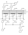
- FIG. 3 is a cross-sectional view showing a schematic diagram of an exemplary device structure of a pixel 10 according to the present embodiment.
- the above-mentioned signal detection transistor 24, address transistor 26, and reset transistor 28 are formed on a semiconductor substrate 20.
- the semiconductor substrate 20 is not limited to a substrate made entirely of semiconductor material.
- the semiconductor substrate 20 may be an insulating substrate having a semiconductor layer provided on the surface on which the photosensitive region is formed.
- a P-type silicon (Si) substrate is used as the semiconductor substrate 20.
- the semiconductor substrate 20 has impurity regions 26s, 24s, 24d, 28d, and 28s, and an element isolation region 20t for electrical isolation between the pixels 10.
- the impurity regions 26s, 24s, 24d, 28d, and 28s are N-type regions.
- the element isolation region 20t is also provided between the impurity region 24d and the impurity region 28d.
- the element isolation region 20t is formed, for example, by ion implantation of an acceptor under predetermined implantation conditions.
- the impurity regions 26s, 24s, 24d, 28d, and 28s are, for example, diffusion layers formed in the semiconductor substrate 20.
- the signal detection transistor 24 includes impurity regions 24s and 24d and a gate electrode 24g.
- the impurity region 24s functions, for example, as a source region of the signal detection transistor 24.
- the impurity region 24d functions, for example, as a drain region of the signal detection transistor 24.
- the channel region of the signal detection transistor 24 is formed between the impurity region 24s and the impurity region 24d.
- the address transistor 26 includes impurity regions 26s and 24s, and a gate electrode 26g connected to an address control line 46 (see FIG. 2).
- the signal detection transistor 24 and the address transistor 26 are electrically connected to each other by sharing the impurity region 24s.
- the impurity region 26s functions as, for example, a source region of the address transistor 26.
- the impurity region 26s is connected to a vertical signal line 47 (see FIG. 2), not shown in FIG. 3.
- the gate electrodes 24g, 26g, and 28g are each formed using a conductive material.
- the conductive material is, for example, polysilicon that has been doped with impurities to make it conductive, but may also be a metal material.
- An interlayer insulating layer 50 is disposed on the semiconductor substrate 20 so as to cover the signal detection transistor 24, the address transistor 26, and the reset transistor 28.
- the interlayer insulating layer 50 is formed of an insulating material such as silicon oxide.
- a wiring layer 56 may be disposed in the interlayer insulating layer 50.
- the wiring layer 56 is formed of a metal such as copper.
- the wiring layer 56 may include, for example, wiring such as the vertical signal line 47 described above as part of it.
- the number of insulating layers in the interlayer insulating layer 50 and the number of layers included in the wiring layer 56 disposed in the interlayer insulating layer 50 can be set arbitrarily and are not limited to the example shown in FIG. 3.
- the above-mentioned photoelectric conversion unit 13 is disposed on the interlayer insulating layer 50.
- a plurality of pixels 10 constituting a pixel array PA are formed on a semiconductor substrate 20.
- a plurality of pixels 10 arranged two-dimensionally on the semiconductor substrate 20 form a pixel region, which is a photosensitive region.
- the distance between two adjacent pixels 10 can be, for example, approximately 2 ⁇ m.
- the distance between two adjacent pixels 10 is also called the "pixel pitch.”
- the photoelectric conversion unit 13 includes a pixel electrode 11, a counter electrode 12, and a photoelectric conversion layer 15 disposed therebetween.
- the photoelectric conversion unit 13 further includes a shield electrode 16.
- the pixel electrode 11 is an example of a first electrode
- the counter electrode 12 is an example of a second electrode
- the shield electrode 16 is an example of a third electrode.
- the counter electrode 12, the photoelectric conversion layer 15, and the shield electrode 16 are formed across multiple pixels 10.
- the pixel electrode 11 is provided for each pixel 10, and is electrically isolated from the pixel electrodes 11 of the other pixels 10 by being spatially separated from the pixel electrodes 11 of the other adjacent pixels 10.
- the counter electrode 12 is disposed opposite the pixel electrode 11 with the photoelectric conversion layer 15 interposed therebetween.
- the counter electrode 12 is, for example, a transparent electrode formed from a transparent conductive material.
- the counter electrode 12 is disposed on the side of the photoelectric conversion layer 15 where light is incident. Therefore, light transmitted through the counter electrode 12 is incident on the photoelectric conversion layer 15.
- the light detected by the image sensor 110 is not limited to light within the wavelength range of visible light (e.g., 380 nm or more and 780 nm or less).
- transparent means that at least a part of the light in the wavelength range to be detected is transmitted, and it is not essential that light is transmitted over the entire wavelength range of visible light.
- the counter electrode 12 can be made of a transparent conducting oxide (TCO) such as ITO, IZO, AZO, FTO, SnO 2 , TiO 2 , or ZnO 2 .
- TCO transparent conducting oxide
- the photoelectric conversion layer 15 receives incident light and generates hole-electron pairs, which are pairs of electric charges.
- the photoelectric conversion layer 15 is formed, for example, from an organic material. Specific examples of materials that make up the photoelectric conversion layer 15 will be described later.
- the counter electrode 12 is connected to the sensitivity control line 42 connected to the voltage supply circuit 32.
- the counter electrode 12 is formed across a plurality of pixels 10. Therefore, it is possible to apply a sensitivity control voltage of a desired magnitude from the voltage supply circuit 32 to a plurality of pixels 10 at once through the sensitivity control line 42. If a sensitivity control voltage of a desired magnitude can be applied from the voltage supply circuit 32, the counter electrode 12 may be provided separately for each pixel 10, or may be provided separately for each pixel block consisting of two or more pixels 10, which is a part of the plurality of pixels 10. In other words, the counter electrode 12 may be divided into a plurality of parts. In the example shown in FIG.
- the sensitivity control line 42 connected to the counter electrode 12 is connected to one voltage supply circuit 32, but this is not limited to this.
- a corresponding voltage supply circuit 32 out of the plurality of voltage supply circuits 32 may be connected to each of the plurality of parts of the counter electrode 12 through the sensitivity control line 42.
- the photoelectric conversion layer 15 may be provided separately for each pixel 10, or may be provided separately for each pixel block consisting of two or more pixels 10 that are a portion of the multiple pixels 10. In other words, the photoelectric conversion layer 15 may be divided into multiple parts.
- the voltage supply circuit 32 applies a voltage between the pixel electrode 11 and the counter electrode 12 by supplying a voltage to the counter electrode 12. As will be described in detail later, the voltage supply circuit 32 supplies different voltages to the counter electrode 12 between an exposure period and a non-exposure period, for example.
- the "exposure period” refers to a period during which signal charge, which is one of the positive and negative charges generated by photoelectric conversion, is accumulated in a charge accumulation region, and may also be called the "charge accumulation period.”
- non-exposure period a period other than an exposure period during operation of the imaging device is referred to as a "non-exposure period.”
- the “non-exposure period” is not limited to a period during which light is blocked from entering the photoelectric conversion unit 13, but may also include a period during which light is irradiated onto the photoelectric conversion unit 13.
- the “non-exposure period” also includes a period during which signal charge is unintentionally accumulated in the charge accumulation region due to the occurrence of parasitic sensitivity.
- the pixel electrode 11 can collect either the holes or the electrons of the hole-electron pairs generated in the photoelectric conversion layer 15 by photoelectric conversion.
- the voltage applied between the pixel electrode 11 and the counter electrode 12 is also called the "bias voltage”.
- the signal charge collected by the pixel electrode 11 is stored in the charge accumulation region. For example, when holes are used as signal charges, it is possible to selectively collect holes by the pixel electrode 11 by making the potential of the counter electrode 12 higher than that of the pixel electrode 11.
- the counter electrode 12 is connected to the above-mentioned sensitivity control line 42, for example, in the peripheral region of the pixel array PA, and a voltage is supplied from the voltage supply circuit 32. Note that the counter electrode 12 may also be supplied with a voltage from the voltage supply circuit 32 via a via contact penetrating the photoelectric conversion layer 15 and the wiring layer 56.
- the pixel electrode 11 facing the counter electrode 12 collects one of the positive and negative charges generated by photoelectric conversion in the photoelectric conversion layer 15 by applying an appropriate bias voltage between the counter electrode 12 and the pixel electrode 11 as described above.
- the pixel electrode 11 is made of, for example, a metal such as aluminum or copper, a metal nitride, or polysilicon that has been doped with impurities to give it conductivity.
- the pixel electrode 11 may be a light-shielding electrode.
- a TaN electrode with a thickness of 100 nm as the pixel electrode 11, sufficient light-shielding properties can be achieved.
- a light-shielding film may be formed in the interlayer insulating layer 50 using the above-mentioned wiring layer 56.
- the pixel electrode 11 is connected to the gate electrode 24g of the signal detection transistor 24 via the plug 52, the wiring 53, and the contact plug 54.
- the gate of the signal detection transistor 24 has an electrical connection with the pixel electrode 11.
- the plug 52 and the wiring 53 are made of a metal such as copper.
- the plug 52, the wiring 53, and the contact plug 54 constitute at least a part of the charge storage node 41 (see FIG. 2) between the signal detection transistor 24 and the photoelectric conversion unit 13.
- the wiring 53 may be a part of the wiring layer 56.
- the pixel electrode 11 is also connected to the impurity region 28d via the plug 52, the wiring 53, and the contact plug 55. In the configuration illustrated in FIG.
- the gate electrode 24g of the signal detection transistor 24, the plug 52, the wiring 53, the contact plugs 54 and 55, and the impurity region 28d, which is one of the source region and the drain region of the reset transistor 28, function as a charge storage region that stores the signal charge collected by the pixel electrode 11.
- a voltage corresponding to the amount of signal charge accumulated in the charge accumulation region is applied to the gate of the signal detection transistor 24.
- the voltage applied to the gate of the signal detection transistor 24 corresponds to the potential of the charge accumulation node 41.
- the signal detection transistor 24 amplifies this voltage.
- the voltage amplified by the signal detection transistor 24 is selectively read out as a signal voltage via the address transistor 26.
- the shield electrode 16 is disposed opposite the counter electrode 12 with the photoelectric conversion layer 15 sandwiched therebetween. Although not shown in FIG. 3, as described above, the shield electrode 16 is connected to the shield wire 17, and a voltage is applied from the shield voltage supply circuit 18 via the shield wire 17. A portion of the shield wire 17 may be included in the wiring layer 56. Although not shown in FIG. 3, the shield electrode 16 may be connected to the wiring layer 56 via a contact or the like.
- FIG. 4 is a plan view showing an example of a planar layout of the pixel electrode 11 and the shield electrode 16. Note that in FIG. 4, illustrations other than the pixel electrode 11 and the shield electrode 16 are omitted. Also, in FIG. 4, for ease of viewing, the pixel electrode 11 and the shield electrode 16 are shaded in the same way as the pixel electrode 11 and the shield electrode 16 shown in the cross section of FIG. 3.
- the pixel electrodes 11 are arranged, for example, in an array.
- the shield electrodes 16 are disposed between adjacent pixel electrodes 11 in a planar view.
- the shield electrodes 16 surround the pixel electrodes 11 in a planar view.
- the shield electrodes 16 are disposed in a lattice shape in a planar view, and a pixel electrode 11 is disposed within each lattice.
- the shield electrodes 16 are formed, for example, collectively across multiple pixels 10, and all pixels 10 have the same potential.
- the shield electrode 16 may be provided separately for each pixel 10, or for each pixel block consisting of two or more pixels 10 that are a part of the multiple pixels 10. In other words, the shield electrode 16 may be divided into multiple parts. In the example shown in FIG. 2, the shield wire 17 connected to the shield electrode 16 is connected to one shield voltage supply circuit 18, but this is not limited to this. When the shield electrode 16 is divided into multiple parts, each of the multiple parts of the shield electrode 16 may be connected to a corresponding one of the multiple shield voltage supply circuits 18 via the shield wire 17.
- the voltage applied to the shield electrode 16 can be used to suppress the movement of signal charges between pixels 10, that is, so-called crosstalk. Therefore, color mixing can be suppressed even if the photoelectric conversion layer 15 is not physically separated.
- the voltage applied to the shield electrode 16 is set, for example, so that the potential of the shield electrode 16 is higher than the potential of the pixel electrode 11. For example, a voltage higher than the reset voltage Vr is applied to the shield electrode 16. This makes it easier for holes to move to the pixel electrodes 11 surrounded by the shield electrode 16 in a planar view, and it is possible to suppress the movement of holes beyond the shield electrode 16 to the pixel electrode 11 of the adjacent pixel 10.
- the voltage applied to the shield electrode 16 may be set so that the potential of the shield electrode 16 is lower than the potential of the pixel electrode 11.
- a voltage lower than the reset voltage Vr is applied to the shield electrode 16.
- the shield electrode 16 is formed, for example, from a metal such as aluminum or copper, a metal nitride, or polysilicon that has been doped with impurities to make it conductive.
- the shield electrode 16 may be a light-shielding electrode.
- the shield electrode 16 may be formed from the same material as the pixel electrode 11.
- the shield electrode 16 and the pixel electrode 11 may be formed simultaneously in the same process.
- At least one of the circuits of the peripheral circuits of the image sensor 110 described above, the current change detection circuit 130, and the drive control circuit 140 may be formed on the same semiconductor substrate 20 as the image sensor 110.
- the photoelectric conversion layer 15 As described above, by irradiating the photoelectric conversion layer 15 with light and applying a bias voltage between the pixel electrode 11 and the counter electrode 12, one of the positive and negative charges generated by photoelectric conversion can be collected by the pixel electrode 11, and the collected charges can be stored in the charge accumulation region.
- a photoelectric conversion unit 13 having a photoelectric conversion layer 15 that exhibits the photocurrent characteristics described below, and by reducing the potential difference between the pixel electrode 11 and the counter electrode 12 to a certain extent, it is possible to suppress the signal charge already accumulated in the charge accumulation region from moving to the counter electrode 12 via the photoelectric conversion layer 15. Furthermore, it is possible to suppress further accumulation of signal charge in the charge accumulation region after reducing the potential difference.
- a global shutter function can be realized without providing a separate element such as a transfer transistor in each of the multiple pixels 10 as in the technology described in Patent Document 1.
- An example of the operation of the imaging device 100 will be described later.
- normal rolling shutter drive is also possible by keeping the magnitude of the bias voltage applied to the photoelectric conversion unit 13 constant and setting the completion of resetting the pixel 10 as the start of the exposure period.
- the photoelectric conversion layer 15 includes, for example, a semiconductor material.
- a semiconductor material for example, an organic semiconductor material is used as the semiconductor material.
- the photoelectric conversion layer 15 contains, for example, tin phthalocyanine represented by the following general formula (1).
- tin phthalocyanine represented by the following general formula (1) may be simply referred to as "tin phthalocyanine”.
- R 1 to R 24 each independently represent a hydrogen atom or a substituent.
- the substituent is not limited to a specific substituent.
- the substituent may be a deuterium atom, a halogen atom, an alkyl group (including a cycloalkyl group, a bicycloalkyl group, and a tricycloalkyl group), an alkenyl group (including a cycloalkenyl group and a bicycloalkenyl group), an alkynyl group, an aryl group, a heterocyclic group (which may also be called a heterocyclic group), a cyano group, a hydroxy group, a nitro group, a carboxy group, an alkoxy group, an aryloxy group, a silyloxy group, a heterocyclic oxy group, an acyloxy group, a carbamoyloxy group, an alkoxycarbonyloxy group, an aryloxycarbonyloxy group, an amino
- the substituent may be an amino group, an aryloxycarbonylamino group, a sulfamoylamino group, an alkylsulfonylamino group, an arylsulfonylamino group, a mercapto group, an alkylthio group, an arylthio group, a heterocyclic thio group, a sulfamoyl group, a sulfo group, an alkylsulfinyl group, an arylsulfinyl group, an alkylsulfonyl group, an arylsulfonyl group, an acyl group, an aryloxycarbonyl group, an alkoxycarbonyl group, a carbamoyl group, an arylazo group, a heterocyclic azo group, an imido group, a phosphino group, a phosphinyl group, a phosphinyloxy group, a
- the tin phthalocyanine represented by the above general formula (1) a commercially available product can be used.
- the tin phthalocyanine represented by the above general formula (1) can be synthesized from a naphthalene derivative represented by the following general formula (2) as a starting material, as shown in, for example, Patent Document 3.
- R 25 to R 30 in the general formula (2) can be the same substituents as R 1 to R 24 in the general formula (1).
- R1 to R24 may be hydrogen atoms or deuterium atoms, 16 or more of R1 to R24 may be hydrogen atoms or deuterium atoms, or all may be hydrogen atoms or deuterium atoms.
- the tin phthalocyanine represented by the following formula (3) is advantageous from the viewpoint of ease of synthesis.
- Tin phthalocyanine represented by the above general formula (1) has absorption in the wavelength range of approximately 200 nm or more and 1100 nm or less.
- tin phthalocyanine represented by the above formula (3) has an absorption peak at a wavelength of approximately 870 nm, as shown in Figure 5.
- Figure 5 shows an example of the absorption spectrum of a photoelectric conversion layer containing tin phthalocyanine represented by the above formula (3). Note that the absorption spectrum was measured using a sample in which a photoelectric conversion layer with a thickness of 30 nm was laminated on a quartz substrate.
- a photoelectric conversion layer formed from a material containing tin naphthalocyanine has absorption in the visible light wavelength region and the near infrared wavelength region.
- a material containing tin naphthalocyanine as the material constituting the photoelectric conversion layer 15, for example, an optical sensor capable of detecting near infrared light can be realized.
- a naphthalocyanine derivative in which the central metal is not tin but another metal such as silicon or germanium may be used.
- an axial ligand may be coordinated to the central metal of the naphthalocyanine derivative.
- FIG. 6 is a cross-sectional view showing a schematic example of the configuration of the photoelectric conversion layer 15.
- the photoelectric conversion layer 15 has a hole blocking layer 15h, a photoelectric conversion structure 15A, and an electron blocking layer 15e.
- the hole blocking layer 15h is disposed between the photoelectric conversion structure 15A and the counter electrode 12, and the electron blocking layer 15e is disposed between the photoelectric conversion structure 15A and the pixel electrode 11.
- the photoelectric conversion layer 15 does not have to have at least one of the hole blocking layer 15h and the electron blocking layer 15e.
- the photoelectric conversion structure 15A shown in FIG. 6 includes, for example, at least one of a p-type semiconductor and an n-type semiconductor.
- the photoelectric conversion structure 15A has a p-type semiconductor layer 150p, an n-type semiconductor layer 150n, and a mixed layer 150m sandwiched between the p-type semiconductor layer 150p and the n-type semiconductor layer 150n.
- the p-type semiconductor layer 150p is disposed between the electron blocking layer 15e and the mixed layer 150m, and has a function of photoelectric conversion and/or hole transport.
- the n-type semiconductor layer 150n is disposed between the hole blocking layer 15h and the mixed layer 150m, and has a function of photoelectric conversion and/or electron transport.
- the mixed layer 150m may include at least one of a p-type semiconductor and an n-type semiconductor.
- the p-type semiconductor layer 150p contains an organic p-type semiconductor
- the n-type semiconductor layer 150n contains an organic n-type semiconductor. That is, the photoelectric conversion structure 15A contains an organic photoelectric conversion material containing tin phthalocyanine represented by the above-mentioned general formula (1), an organic p-type semiconductor, and an organic n-type semiconductor.
- An organic p-type semiconductor is a donor organic semiconductor, and is mainly represented by a hole-transporting organic compound, and refers to an organic compound that has the property of easily donating electrons. More specifically, an organic p-type semiconductor is a donor organic compound, and refers to the organic compound that has the smaller ionization potential when two organic materials are used in contact. Therefore, any organic compound that has electron-donating properties can be used as a donor organic compound.
- donor organic compounds include triarylamine compounds, benzidine compounds, pyrazoline compounds, styrylamine compounds, hydrazone compounds, triphenylmethane compounds, carbazole compounds, polysilane compounds, thiophene compounds, phthalocyanine compounds, naphthalocyanine compounds, subphthalocyanine compounds, cyanine compounds, merocyanine compounds, oxonol compounds, polyamine compounds, indole compounds, pyrrole compounds, pyrazole compounds, polyarylene compounds, condensed aromatic carbon ring compounds (naphthalene derivatives, anthracene derivatives, phenanthrene derivatives, tetracene derivatives, pyrene derivatives, perylene derivatives, fluoranthene derivatives), and metal complexes having nitrogen-containing heterocyclic compounds as ligands.
- the donor organic semiconductor is not limited to these, and any organic compound having a smaller ionization potential than the organic compound used as the acceptor organic semiconductor described later can be used as the donor organic semiconductor.
- the above-mentioned tin naphthalocyanine is an example of an organic p-type semiconductor material.
- Organic n-type semiconductors are acceptor organic semiconductors, and are mainly represented by electron transporting organic compounds, and refer to organic compounds that have the property of readily accepting electrons. More specifically, organic n-type semiconductors are acceptor organic compounds, and refer to the organic compound that has the greater electron affinity when two organic compounds are used in contact. Therefore, any organic compound that has electron accepting properties can be used as an acceptor organic compound.
- acceptor organic compound examples include fullerene, fullerene derivatives, condensed aromatic carbon ring compounds (naphthalene derivatives, anthracene derivatives, phenanthrene derivatives, tetracene derivatives, pyrene derivatives, perylene derivatives, and fluoranthene derivatives), 5- to 7-membered heterocyclic compounds containing a nitrogen atom, an oxygen atom, or a sulfur atom (e.g., pyridine, pyrazine, pyrimidine, pyridazine, triazine, quinoline, quinoxaline, quinazoline, phthalazine, cinnoline, isoquinoline, pteridine, acridine, phenazine, phenanthroline, tetrazole, pyrazoline, and the like).
- condensed aromatic carbon ring compounds e.g., pyridine, pyrazine, pyrimidine, pyridazin
- organic semiconductor examples include metal complexes having a ligand such as aryl, imidazole, thiazole, oxazole, indazole, benzimidazole, benzotriazole, benzoxazole, benzothiazole, carbazole, purine, triazolopyridazine, triazolopyrimidine, tetrazaindene, oxadiazole, imidazopyridine, pyrrolidine, pyrrolopyridine, thiadiazolopyridine, dibenzazepine, tribenzazepine, etc.), polyarylene compounds, fluorene compounds, cyclopentadiene compounds, silyl compounds, and nitrogen-containing heterocyclic compounds.
- the organic semiconductor can be any organic compound that has a larger electron affinity than the organic compound used as the donor organic compound, as described above.
- the mixed layer 150m may be, for example, a bulk heterojunction structure layer including a p-type semiconductor and an n-type semiconductor.
- tin phthalocyanine represented by the above general formula (1) may be used as the p-type semiconductor material.
- n-type semiconductor material for example, fullerene and/or a fullerene derivative may be used.
- the material constituting the p-type semiconductor layer 150p may be the same as the p-type semiconductor material contained in the mixed layer 150m.
- the material constituting the n-type semiconductor layer 150n may be the same as the n-type semiconductor material contained in the mixed layer 150m.
- Patent Document 4 Japanese Patent No. 5553727.
- Japanese Patent No. 5553727 the entire disclosure of Japanese Patent No. 5553727 is incorporated herein by reference.
- the photoelectric conversion layer 15 that uses tin phthalocyanine and is sensitive to near-infrared light has been described, but the material contained in the photoelectric conversion layer 15 is not limited to photoelectric conversion materials that are sensitive to near-infrared light.
- the photoelectric conversion layer 15 can become a photoelectric conversion layer 15 that is sensitive to visible light by using subphthalocyanine as a p-type semiconductor and fullerene and/or a fullerene derivative as an n-type semiconductor.
- FIG. 7 is a diagram showing exemplary photocurrent characteristics of the photoelectric conversion unit 13.
- the solid line graph shows exemplary current-voltage characteristics (I-V characteristics) of the photoelectric conversion unit 13 when it is irradiated with light, i.e., when it is bright.
- FIG. 7 also shows, by a dashed line, an example of the I-V characteristics of the photoelectric conversion unit 13 when it is not irradiated with light, i.e., when it is dark.
- Figure 7 shows the change in current density between the main surfaces of the photoelectric conversion layer 15 when the bias voltage applied between the pixel electrode 11 and the counter electrode 12 of the photoelectric conversion unit 13 is changed under a constant illuminance.
- the forward and reverse directions of the bias voltage are defined as follows.
- the bias voltage that makes the potential of the p-type semiconductor layer higher than that of the n-type semiconductor layer is defined as the forward bias voltage.
- the bias voltage that makes the potential of the p-type semiconductor layer lower than that of the n-type semiconductor layer is defined as the reverse bias voltage.
- a bias voltage that makes the potential of the main surface side where more p-type semiconductors than n-type semiconductors appear is higher than the potential of the main surface side where more n-type semiconductors than p-type semiconductors appear is defined as a forward bias voltage.
- a voltage that makes the potential of the counter electrode 12 higher than the potential of the pixel electrode 11 is a reverse bias voltage
- a voltage that makes the potential of the counter electrode 12 lower than the potential of the pixel electrode 11 is a forward bias voltage
- the photocurrent characteristics of the photoelectric conversion unit 13 are roughly characterized by three voltage ranges, from the first voltage range to the third voltage range.
- the first voltage range is a reverse bias voltage range, and is a voltage range in which the absolute value of the output current density increases as the reverse bias voltage increases.
- the first voltage range can be said to be a voltage range in which the photocurrent increases as the bias voltage applied between the pixel electrode 11 and the counter electrode 12 increases.
- the second voltage range is a forward bias voltage range, and is a voltage range in which the output current density increases as the forward bias voltage increases. In other words, the second voltage range is a voltage range in which the photocurrent in the opposite direction to the first voltage range increases as the bias voltage applied between the pixel electrode 11 and the counter electrode 12 increases.
- the third voltage range is a voltage range between the first voltage range and the second voltage range.
- the first to third voltage ranges can also be distinguished by the slope of the graph of the photocurrent characteristics when linear vertical and horizontal axes are used.
- the average slopes of the graphs in the first and second voltage ranges are shown by dashed and dotted lines L1 and L2, respectively.
- the rates of change of the output current density with respect to an increase in the bias voltage in the first, second, and third voltage ranges are different from each other.
- the third voltage range is also defined as a voltage range in which the rate of change of the output current density with respect to the bias voltage is smaller than the rate of change in the first voltage range and the rate of change in the second voltage range.
- the third voltage range may be determined based on the position of the rise or fall in the graph showing the IV characteristics.
- the third voltage range is, for example, larger than -1V and smaller than +1V.
- the absolute value of the current density is, for example, 100 ⁇ A/cm 2 or less.
- the difference between the dark current and the light current in the third voltage range is smaller than the difference between the dark current and the light current in the first voltage range and the difference between the dark current and the light current in the second voltage range.
- the dark current is the current that flows through the photoelectric conversion layer 15 when no light is irradiated
- the light current is the current that flows through the photoelectric conversion layer 15 when light is irradiated.
- I-V characteristics of the photoelectric conversion unit 13 shown in FIG. 7 are just an example, and the desired I-V characteristics can be achieved by adjusting the configuration and materials of the photoelectric conversion layer 15 described above.
- FIG. 8 is a diagram for explaining an example of the operation of normal imaging drive in the imaging device 100 according to this embodiment.
- FIG. 8 shows the timing of the falling or rising edge of the synchronization signal, the change over time in the magnitude of the bias voltage applied to the photoelectric conversion unit 13, and the timing of reset and exposure in each row of the pixel array PA (see FIG. 2).
- the top graph (a) in FIG. 8 shows the timing of the fall or rise of the vertical synchronization signal Vss.
- Graph (b) in FIG. 8 shows the timing of the fall or rise of the horizontal synchronization signal Hss.
- Graph (c) in FIG. 8 shows an example of the change over time of the voltage Vb applied to the counter electrode 12 from the voltage supply circuit 32 via the sensitivity control line 42.
- Graph (d) in FIG. 8 shows the change over time of the potential ⁇ of the counter electrode 12, that is, the bias voltage, when the potential of the pixel electrode 11 is used as a reference.
- the double-headed arrow G3 in the graph (d) of the potential ⁇ in FIG. 8 indicates the third voltage range described above.
- Chart (e) in FIG. 8 shows the timing of reset and exposure in each row of the pixel array PA.
- the charge storage region of each pixel 10 in the pixel array PA is reset, and the pixel signal after reset is read out. For example, as shown in FIG. 8, resetting of multiple pixels 10 belonging to row R0 is started (time t0) based on the vertical synchronization signal Vss. Note that the rectangle with low-density halftone dots in chart (e) of FIG. 8 shows a schematic representation of the signal readout period. This readout period may include a reset period for resetting the potential of the charge storage region of the pixel 10 as part of it.
- the address transistor 26 whose gate is connected to the address control line 46 of the R0th row is turned ON by controlling the potential of the address control line 46 of the R0th row, and further, the reset transistor 28 whose gate is connected to the reset control line 48 of the R0th row is turned ON by controlling the potential of the reset control line 48 of the R0th row.
- This connects the charge storage node 41 and the reset voltage line 44, and the reset voltage Vr is supplied to the charge storage region. That is, the potentials of the charge storage node 41, the gate electrode 24g of the signal detection transistor 24, and the pixel electrode 11 of the photoelectric conversion unit 13 are reset to the reset voltage Vr.
- a pixel signal corresponding to the potential of the charge storage region after reset is read out from the pixel 10 of the R0th row via the vertical signal line 47.
- the pixel signal obtained at this time is a pixel signal corresponding to the magnitude of the reset voltage Vr.
- the reset transistor 28 and the address transistor 26 are turned OFF.
- the pixel signal may be read out before resetting.
- resetting of the pixels 10 in each row from row R0 to row R7 is performed sequentially row by row in accordance with the horizontal synchronization signal Hss.
- the interval between pulses of the horizontal synchronization signal Hss in other words, the period from when a row is selected to when the next row is selected, may be referred to as the "1H period.”
- the period from time t0 to time t1 corresponds to the 1H period.
- a voltage V3 is applied from the voltage supply circuit 32 to the counter electrode 12 so that the voltage applied between the pixel electrode 11 and the counter electrode 12 is within the above-mentioned third voltage range.
- a bias voltage within the third voltage range is applied between the pixel electrode 11 and the counter electrode 12.
- the period indicated by a rectangle with low density halftone dots and a rectangle with high density halftone dots represents the non-exposure period.
- a bias voltage within the third voltage range is applied between the pixel electrode 11 and the counter electrode 12 during the non-exposure period.
- the voltage V3 for applying the bias voltage within the third voltage range between the pixel electrode 11 and the counter electrode 12 is not limited to 0 V.
- the voltage V3 is set, for example, in response to the reset voltage Vr so that the bias voltage is a voltage within the third voltage range.
- an exposure period is started based on the horizontal synchronization signal Hss (time t9).
- the white rectangles represent the exposure period in each row.
- the exposure period is started by the voltage supply circuit 32 switching the voltage applied to the counter electrode 12 to a voltage Ve different from the voltage V3.
- the voltage Ve is, for example, a voltage such that the bias voltage applied between the pixel electrode 11 and the counter electrode 12 falls within the above-mentioned first voltage range, for example, about 10 V.
- the signal charges in the photoelectric conversion layer 15, in this example, holes are collected by the pixel electrode 11 and stored in a charge storage region including the charge storage node 41.
- the voltage Ve is set, for example, according to the reset voltage Vr so that the bias voltage falls within the first voltage range.
- the voltage supply circuit 32 switches the voltage applied to the counter electrode 12 back to voltage V3, thereby ending the exposure period (time t13).
- the voltage applied to the counter electrode 12 is switched between voltage V3 and voltage Ve, thereby switching between exposure and non-exposure periods.
- the start (time t9) and end (time t13) of the exposure period in this example are common to all pixels 10 included in the pixel array PA.
- the operation described here is an example in which the global shutter method is applied to the imaging element 110, and the imaging device 100 is driven by the global shutter method in which the exposure period is determined by changing the voltage applied by the voltage supply circuit 32 between the pixel electrode 11 and the counter electrode 12.
- pixel signals are read out from the pixels 10 belonging to each row of the pixel array PA.
- signal charges are read out from the pixels 10 belonging to each row from row R0 to row R7 in sequence, row by row.
- the period from when a pixel 10 belonging to a certain row is selected to when a pixel 10 belonging to that row is selected again may be referred to as the "1V period.”
- the period from time t0 to time t15 corresponds to the 1V period.
- the 1V period is, for example, one frame period.
- the address transistor 26 of row R0 When the exposure period ends and pixel signals are read from pixels 10 belonging to row R0 starting at time t15, the address transistor 26 of row R0 is first turned ON. This causes a pixel signal corresponding to the amount of charge accumulated in the charge accumulation region during the exposure period, i.e., the potential of the charge accumulation region after the exposure period, to be output to the vertical signal line 47. Following the reading of the pixel signal, the reset transistor 28 may be turned ON to reset the pixel 10. If necessary, the pixel signal may also be read after this reset. After the pixel signal is read, the address transistor 26 is turned OFF, and if the pixel 10 is reset, the reset transistor 28 is also turned OFF.
- a signal from which fixed noise has been removed is obtained by taking the difference between the pixel signals after reset read between time t0 and time t9.
- This removal of fixed noise is performed, for example, by the column signal processing circuit 37.
- the removal of fixed noise may be performed before or after AD conversion of the pixel signals.
- a signal is read from the column signal processing circuit 37 by the horizontal signal readout circuit 38, and is processed by a signal processing circuit (not shown) or the like as necessary, and output to the outside of the imaging device 100.
- a signal from which fixed noise has been removed may be obtained by taking the difference between the pixel signal read after the reset and the pixel signal read before the reset.
- the voltage applied to the counter electrode 12 is changed back to voltage V3, so that the photoelectric conversion unit 13 after the accumulation of signal charge in the charge accumulation region is in a state in which a bias voltage within the third voltage range is applied.
- a bias voltage within the third voltage range it is possible to suppress the movement of signal charge already accumulated in the charge accumulation region to the counter electrode 12 via the photoelectric conversion layer 15.
- by applying a bias voltage within the third voltage range to the photoelectric conversion unit 13 it is possible to hold the signal charge accumulated during the exposure period in the charge accumulation region. In other words, it is possible to suppress the occurrence of negative parasitic sensitivity caused by the loss of signal charge from the charge accumulation region.
- the start and end of the exposure period are controlled by the voltage Vb applied to the opposing electrode 12. That is, according to this embodiment, a global shutter function can be realized without providing a transfer transistor or the like in each pixel 10.
- the electronic shutter is executed by controlling the voltage Vb without transferring signal charge via a transfer transistor, allowing for faster operation.
- this is also advantageous for miniaturizing pixels.
- the imaging device 100 may be driven by the rolling shutter method in normal imaging drive.
- the voltage applied to the opposing electrode 12 is constant at voltage Ve.
- the end of the reset operation marks the start of the exposure period
- the start of the subsequent readout operation marks the end of the exposure period.
- the exposure period of the pixel 10 belonging to row R0 is from time t1 to time t15.
- the current measurement circuit 19 that measures the current flowing in the photoelectric conversion unit 13.
- the current change detection circuit 130 detects a change in the current flowing in the photoelectric conversion unit 13 measured by the current measurement circuit 19, and it is possible to detect a moving object based on the detected change in current.
- the current measurement circuit 19 is disposed on the wiring connected to the photoelectric conversion unit 13, and measures the current flowing through the photoelectric conversion unit 13.
- the photoelectric conversion unit 13 has the counter electrode 12, the shield electrode 16, and the pixel electrode 11 as electrodes connected to the wiring, and therefore the current measurement circuits 19a, 19b, and 19c are connected to any of these electrodes.
- the current measurement circuit 19a is an example of a first current measurement circuit, and is a current measurement circuit connected to the counter electrode 12.
- the current measurement circuit 19b is an example of a second current measurement circuit, and is a current measurement circuit connected to the shield electrode 16.
- the current measurement circuit 19c is an example of a third current measurement circuit, and is a current measurement circuit connected to the pixel electrode 11.
- the current measurement circuit 19a is connected to the counter electrode 12.
- the current measurement circuit 19a is also connected to the voltage supply circuit 32 and is provided in the middle of the wiring path connecting the voltage supply circuit 32 and the counter electrode 12, that is, the sensitivity control line 42. Therefore, the current measurement circuit 19a measures the current flowing in the photoelectric conversion unit 13 by measuring the current flowing between the counter electrode 12 and the voltage supply circuit 32. This makes it possible to measure the current flowing in the photoelectric conversion unit 13 using existing wiring, which makes it possible to suppress the complexity of the pixel circuit and to miniaturize the pixel 10.
- the current measurement circuit 19a is connected to a common counter electrode 12 for two or more pixels 10, for example, it is possible to measure the current of the photoelectric conversion unit 13 across two or more pixels 10, which increases the measured current and improves the accuracy of detecting changes in current.
- the current measurement circuit 19a may be disposed in the voltage supply circuit 32. In other words, the current measurement circuit 19a may be part of the voltage supply circuit 32.
- the counter electrode 12 is divided into two parts, and an individual current measurement circuit 19a is connected to each of the two parts of the counter electrode 12.
- the imaging device 100 has multiple current measurement circuits 19a that measure the current flowing through the photoelectric conversion unit 13 of different pixels 10. Therefore, it is possible to measure the current flowing through the photoelectric conversion unit 13 for each region of the pixel 10 that corresponds to the two parts of the counter electrode 12.
- the counter electrode 12 does not have to be divided, and in this case, there may be only one current measurement circuit 19a.
- the current measurement circuit 19b is connected to the shield electrode 16 as described above.
- the current measurement circuit 19b is also connected to the shield voltage supply circuit 18 and is provided in the middle of the wiring path connecting the shield voltage supply circuit 18 and the shield electrode 16, that is, the shield wire 17. Therefore, the current measurement circuit 19b measures the current flowing in the photoelectric conversion unit 13 by measuring the current flowing between the shield electrode 16 and the shield voltage supply circuit 18. This makes it possible to measure the current flowing in the photoelectric conversion unit 13 using existing wiring, which makes it possible to suppress the complexity of the pixel circuit and to miniaturize the pixel 10.
- the current measurement circuit 19b is connected to a common shield electrode 16 for two or more pixels 10, for example, the current of the photoelectric conversion unit 13 can be measured across two or more pixels 10, and the measured current increases, thereby improving the accuracy of detecting changes in current.
- the current measurement circuit 19b may be disposed in the shield voltage supply circuit 18. In other words, the current measurement circuit 19b may be part of the shield voltage supply circuit 18.
- the shield electrode 16 may be divided into multiple parts, and an individual current measurement circuit 19b may be connected to each of the multiple parts of the shield electrode 16.
- a corresponding current measurement circuit 19b may be provided in each of the first wiring path connecting the shield electrode 16 of the pixel 10a and the shield voltage supply circuit 18, which does not overlap with the second wiring path connecting the shield electrode 16 of the pixel 10c different from the pixel 10a and the shield voltage supply circuit 18, and in each of the second wiring path, which does not overlap with the first wiring path.
- the shield line 17 may be branched into multiple parts so as to extend from the shield voltage supply circuit 18 to the shield electrodes 16 of two or more pixels 10, and a current measurement circuit 19b corresponding to each of the multiple parts of the shield line 17 may be provided.
- This individual current measurement circuit 19b individually measures the current flowing in, for example, a pixel region that is divided into two or more parts, such as a pixel region including pixel 10a and a pixel region including pixel 10c.
- the current measurement circuit 19c is connected to the pixel electrode 11 via the reset transistor 28 and the charge storage node 41.
- the current measurement circuit 19c is also connected to the reset voltage source 34 and is provided in the middle of the wiring path connecting the reset voltage source 34 and the pixel electrode 11, that is, the reset voltage line 44. Therefore, the current measurement circuit 19c measures the current flowing in the photoelectric conversion unit 13 by measuring the current flowing between the pixel electrode 11 and the reset voltage source 34. This makes it possible to measure the current flowing in the photoelectric conversion unit 13 using existing wiring, which makes it possible to suppress the complexity of the pixel circuit and to miniaturize the pixel 10.
- the current of the photoelectric conversion unit 13 can be measured across two or more pixels 10, which increases the measured current and improves the accuracy of detecting changes in current.
- the current flowing in the photoelectric conversion unit 13 is detected by turning on the reset transistor 28 to allow a current to flow in the current measurement circuit 19c.
- the current measurement circuit 19c may be disposed within the reset voltage source 34. In other words, the current measurement circuit 19c may be part of the reset voltage source 34.
- the reset voltage line 44 may be branched into multiple parts so as to go from the reset voltage source 34 to the charge storage nodes 41 of two or more pixels 10, and a current measurement circuit 19c corresponding to each of the multiple parts of the reset voltage line 44 may be provided.
- the individual current measurement circuits 19c individually measure the current flowing in pixel regions divided into two or more, for example, the pixel region including the pixel 10a and the pixel region including the pixel 10c.
- the reset transistors 28 can be switched ON and OFF.
- the current measurement circuit 19c can detect the current flowing through the photoelectric conversion units 13 of only the pixels 10 that correspond to the reset transistors 28 that are turned ON.
- the current measurement circuit 19 can be a measurement circuit used in a known ammeter, such as a measurement circuit using a shunt resistor or a measurement circuit using a magnetic field, and is not particularly limited.
- the current measurement circuit 19 includes, for example, a shunt resistor, an amplifier circuit that amplifies the potential difference generated by the shunt resistor, and an AD conversion circuit that AD converts the output of the amplifier circuit, and outputs the AD converted value at a predetermined sampling interval.
- the current measurement circuit 19 may also include an integrator for peak holding the output of the amplifier circuit. In this case, the AD conversion circuit AD converts the output of the amplifier circuit integrated by the integrator, and resets the integrator at a predetermined interval.
- the number of current measurement circuits 19 is, for example, less than the number of pixels 10.
- the current measurement circuit 19 is provided in common for two or more pixels 10, and can measure the current flowing in the photoelectric conversion unit 13 of a pixel region including two or more pixels 10. This makes it possible to miniaturize the circuitry of the imaging device 100 and reduce power consumption in the operation of detecting changes in the current flowing in the photoelectric conversion unit 13. Furthermore, the amount of current measured by the current measurement circuit 19 also increases, making it easier to detect changes in current.
- the voltage Vb supplied from the voltage supply circuit 32 is supplied so as to be lower or higher than the shield voltage Vs supplied from the shield voltage supply circuit 18 and the reset voltage Vr supplied from the reset voltage source 34.
- voltages are supplied from each voltage supply circuit so that a potential difference occurs between the two electrodes facing each other across the photoelectric conversion layer 15.
- the voltages are set and supplied as follows: voltage Vb is 10 V, shield voltage Vs is 0 V, and reset voltage Vr is 1 V.
- the current measurement circuit 19 outputs the current measurement result, for example, an AD-converted digital value, to the current change detection circuit 130.
- the difference between the voltage Vb and the shield voltage Vs, and the difference between the voltage Vb and the reset voltage Vr may be set to voltages greater than those in normal imaging drive.
- the difference between the voltage Vb and the shield voltage Vs and the difference between the voltage Vb and the reset voltage Vr may be larger than either.
- the difference between the voltage Vb and the shield voltage Vs may be larger than the difference between the voltage Vb and the reset voltage Vr. This makes it easier for a current to flow to the shield electrode 16.
- the voltage Vb is 10V
- the shield voltage Vs is 0V
- the reset voltage Vr is 3V.
- the current measurement circuit 19c measures the current
- the difference between the voltage Vb and the reset voltage Vr may be larger than the difference between the voltage Vb and the shield voltage Vs. This makes it easier for a current to flow to the pixel electrode 11.
- a specific example of this is when the voltage Vb is 10V, the shield voltage Vs is 4V, and the reset voltage Vr is 0.5V.
- the current change detection circuit 130 acquires the output from the current measurement circuit 19 and detects the change in the current flowing through the photoelectric conversion unit 13 measured by the current measurement circuit 19.
- the current change detection circuit 130 detects the change in the current flowing through the photoelectric conversion unit 13 measured by the current measurement circuit 19, for example, by detecting whether or not a change of a predetermined threshold value or more has occurred in the output from the current measurement circuit 19.
- the change in current detected by the current change detection circuit 130 indicates a change that satisfies a predetermined condition, such as a change of a certain threshold value or more, and means a substantial change.
- the change in current detected by the current change detection circuit 130 does not include a change in current caused by a change in the voltage supplied to the photoelectric conversion unit 13, such as when the voltage supplied by various voltage supply circuits that supply voltage to the photoelectric conversion unit 13 changes.
- the current change detection circuit 130 detects changes in current caused by changes in the amount of light incident on the photoelectric conversion unit 13 over time.
- the detection of a change in current by the current change detection circuit 130 may be performed by comparing the previous output value for each AD conversion sampling in the current measurement circuit 19, or by comparing with the average value of a predetermined number of sampled output values. If the current measurement circuit 19 includes an integrator, the current change detection circuit 130 detects a change in current by comparing the difference in the output values from the current measurement circuit 19. In addition, in the case of applications where the background is fixed, such as monitoring applications, the current change detection circuit 130 may detect a change in current by checking whether the output from the current measurement circuit 19 falls outside a predetermined range.
- FIGS. 10A and 10B are diagrams for explaining an example of the current change detection drive operation and output results in the imaging device 100 according to this embodiment.
- a background is present within the imaging range of the imaging device 100, and a ball coming from outside the imaging range is shown crossing the imaging range.
- Fig. 10A shows the state where the ball enters the imaging range from outside
- Fig. 10B shows the state where the ball is in the middle of crossing the imaging range.
- the current change detection circuit 130 can detect the presence of a moving object such as a ball that has entered the imaging range by detecting the change in the current measured by current measurement circuit 19.
- the current change detection circuit 130 can detect the presence of a moving object within the imaging range by detecting a change in the current measured by the current measurement circuit 19.
- the current change detection circuit 130 generates a detection signal related to a moving object moving within the imaging range, for example, based on the detected change in current.
- the detection signal is, for example, a signal indicating whether or not a moving object is present.
- the detection signal may include information related to the amount of change in current detected by the current change detection circuit 130.
- the detection signal generated by the current change detection circuit 130 is, for example, output to the drive control circuit 140 and used to control the drive of the imaging device 100 in the drive control circuit 140.
- the detection signal may also be output to the outside of the imaging device 100.
- the current measurement circuit 19c measures the current, with the reset transistor 28 turned ON, the current measurement circuit 19c measures the current flowing through the wiring connecting the reset voltage source 34 and the reset transistor 28, making it possible for the current change detection circuit 130 to detect a moving object. In this case, it is possible to detect a moving object in any area within the imaging range by determining which pixel 10's reset transistor 28 is turned ON. In addition, by changing the area of the pixel 10 whose reset transistor 28 is turned ON over time, it is possible to detect moving objects in any area within the imaging range while also detecting moving objects in the entire imaging range.
- the counter electrode 12 and the shield electrode 16 may be divided and the imaging range may be divided into areas in advance. This allows the current change detection circuit 130 to detect a moving object for each area. For example, if the counter electrode 12 is divided into four areas, the upper left, upper right, lower right, and lower left, it can detect in which of the four divided areas a moving object is present.
- the current change detection circuit 130 may be set with conditions for detecting changes in the current flowing through the photoelectric conversion unit 13, taking into account such changes in brightness. Specifically, this may involve setting a large detection threshold, analyzing the frequency components of the current change corresponding to the change in brightness of the ambient light, and extracting and detecting only the change in current due to the moving object, and using multiple current measurement circuits 19 to extract and detect the change in current due to the moving object while offsetting the change in current due to ambient light from the current measured by each current measurement circuit 19.
- the accuracy of moving object detection by the current change detection circuit 130 at night and indoors is high. This is because normal indoor lighting has small changes in luminance and is less susceptible to the effects of environmental light such as sunlight, which has large changes in luminance. The same is true at night. Furthermore, at night, the accuracy of moving object detection can be further improved by using a lighting device 200 that emits light including near-infrared rays.
- the drive control circuit 140 controls, for example, the imaging device 100 to perform current change detection drive and normal imaging drive.
- the current change detection drive is a drive mode in which the current change detection circuit 130 detects a change in the current flowing in the photoelectric conversion unit 13
- the normal imaging drive is a drive mode in which the signal detection circuit 14 detects a pixel signal based on the charge generated in the photoelectric conversion unit 13.
- the drive control circuit 140 may switch between the current change detection drive and the normal imaging drive and cause the imaging device 100 to perform them, or may cause the imaging device 100 to perform the current change detection drive and the normal imaging drive simultaneously.
- the drive control circuit 140 switches the drive mode from current change detection drive to normal imaging drive.
- the current change detection circuit 130 may detect a moving object by detecting a change in current. In this way, in current change detection drive, it is possible to operate the imaging device 100 without operating the circuits used for normal imaging, such as in normal imaging drive, making it possible to reduce power consumption. In addition, even when the imaging device 100 is used for surveillance purposes, consideration can be given to privacy.
- the drive control circuit 14 may put at least some of the signal detection circuit 14 and the circuits connected to the signal detection circuit 14 in an off state or a standby state.
- the circuits connected to the signal detection circuit 14 are circuits involved in the output of pixel signals, and include, for example, a circuit that drives the signal detection circuit 14, such as the vertical scanning circuit 36, and circuits that process pixel signals output from the signal detection circuit 14, such as the column signal processing circuit 37 and the horizontal signal readout circuit 38.
- the off state of the circuit is a state in which the power supply is cut off by a switch or the like provided in each circuit.
- the standby state of the circuit is a state in which at least some of the circuits do not operate while power is being supplied, or a state in which the circuits operate with lower power than normal.
- the standby state is, for example, a state in which power consumption is lower than that of normal imaging drive. Therefore, in the current change detection drive, for example, at least some of the circuit elements in the signal detection circuit 14 are not driven, or signal processing is not performed on the pixel signals detected by the signal detection circuit 14. As a result, in current change detection driving, signals derived from pixel signals are not output outside the imaging device 100.
- FIG. 11 is a diagram for explaining a first example of drive mode control in the imaging device 100 according to the present embodiment.
- the drive control circuit 140 first causes the imaging device 100 to perform current change detection drive. In this current change detection drive, no signal is output to the outside of the imaging device 100. Therefore, the image processing unit 300 and the like that performs post-processing of the output from the imaging device 100 do not need to perform image processing, and are in a standby state, for example. This makes it possible to reduce power consumption in post-processing. Also, the capacity required to store images can be reduced. In this case, the image processing unit 300 and the like that performs post-processing of the output from the imaging device 100 may be in an off state.
- the current change detection circuit 130 in the current change detection drive, the current change detection circuit 130 generates a detection signal indicating whether or not a moving object is present within the imaging range, depending on whether or not the current flowing through the photoelectric conversion unit 13 measured by the current measurement circuit 19 has changed, and outputs the detection signal to the drive control circuit 140.
- the current change detection circuit 130 generates a detection signal only when it detects a change in the current flowing through the photoelectric conversion unit 13, and does not need to generate a detection signal when it does not detect a change in the current.
- the detection signal may be output to the outside of the imaging device 100, such as the image processing unit 300.
- the drive control circuit 140 continues the current change detection drive.
- the drive control circuit 140 switches the drive mode from current change detection drive to normal imaging drive.
- normal imaging drive a signal including image data is output to the outside of the imaging device 100.
- the image processing unit 300 which performs post-processing of the output from the imaging device 100, performs image processing and storage, etc. on the image data output from the imaging device 100. In other words, in normal imaging drive, detailed images can be acquired.
- the drive control circuit 140 switches the drive mode from normal imaging drive to current change detection drive after a predetermined, fixed time has elapsed since the imaging device 100 started normal imaging drive. This enables the imaging device 100 to be driven with low power consumption. After switching to current change detection drive, the above operation is performed again.
- the drive control circuit 140 may also cause the imaging device 100 to perform current change detection drive while performing normal imaging drive.
- FIG. 12 is a diagram for explaining a second example of drive mode control in the imaging device 100 according to this embodiment.
- the drive control circuit 140 first causes the imaging device 100 to perform only current change detection drive, and switches to normal imaging drive when the current change detection circuit 130 detects a change in the current flowing in the photoelectric conversion unit 13, which is the same as the first example.
- the drive control circuit 140 while the drive control circuit 140 causes the imaging device 100 to perform normal imaging drive, the drive control circuit 140 also causes the imaging device 100 to perform current change detection drive in parallel and at the same time.
- the drive control circuit 140 continues normal imaging drive. On the other hand, if the current change detection circuit 130 does not detect a change in the current flowing through the photoelectric conversion unit 13 during the current change detection drive during normal imaging drive, the drive control circuit 140 switches from simultaneous normal imaging drive and current change detection drive to current change detection drive only. In this case, since changes in the current flowing through the photoelectric conversion unit 13 are detected even during normal imaging drive, when a moving object is no longer present, the drive mode is switched to one in which only current change detection drive is performed, making it possible to reduce power consumption and the image storage capacity. On the other hand, since images can be acquired at all times while a moving object is present, the moving object can be photographed without interruption.
- the drive control circuit 140 may drive the imaging device 100 in the normal imaging drive by a rolling shutter method in which the voltage supplied by the voltage supply circuit 32 and the shield voltage supply circuit 18 does not change.
- the current change detection circuit 130 detects the change in the current measured by the current measurement circuit 19, for example, by avoiding the timing when the voltage supplied to the photoelectric conversion unit 13 by the voltage supply circuit 32 or the like changes.
- the drive control circuit 140 may also cause the imaging device 100 to perform the current change detection drive and the normal imaging drive simultaneously at all times, regardless of whether the current change detection circuit 130 detects a change in the current flowing through the photoelectric conversion unit 13.
- FIG. 13 is a diagram for explaining a third example of the control of the drive mode in the imaging device 100 according to this embodiment. As shown in FIG. 13, in the third example, the drive control circuit 140 controls the imaging device 100 to perform the current change detection drive and the normal imaging drive simultaneously. That is, in the third example, the operation after the change in the current flowing through the photoelectric conversion unit 13 in the second example is detected is always performed. In this way, the detection of a moving object and the imaging of a normal image are always performed simultaneously.
- the imaging device 100 outputs a signal including image data generated by the normal imaging drive to the outside of the imaging device 100.
- the image processing unit 300 which performs post-processing of the output from the imaging device 100, performs image processing and storage on the image data output from the imaging device 100, etc.
- the image processing unit 300 which performs post-processing of the output from the imaging device 100, does not need to perform image processing, and is in a standby state, for example. This makes it possible to reduce power consumption in post-processing, and also reduces the amount of storage required for images.
- the detection signal generated by the current change detection circuit 130 indicating whether or not a moving object has been detected (or whether or not a change in current has been detected) may be output to the outside of the imaging device 100, such as to the image processing unit 300.
- the imaging device 100 may output a signal including image data, etc., together with the detection signal to the outside of the imaging device 100.
- the image processing unit 300, etc. that receives the output from the imaging device 100, for example, thins out and stores images, such as one every 10 seconds, when a moving object is not detected, and stores images continuously when a moving object is detected.
- the current change detection circuit 130 may limit the pixel area for detecting a moving object in the current change detection drive. For example, when an object such as lighting whose luminance changes or a flag moving in the wind is imaged, the current flowing through the photoelectric conversion unit 13 may change in the same way as a moving object, so that it is possible that these are detected as moving objects and the moving object is always detected.
- the pixel area to be the target for detecting the moving object may be set by excluding the pixel area in which the object such as lighting whose luminance changes or the flag moving in the wind exists in advance.
- the current change detection circuit 130 can detect a moving object that is actually moving without detecting an object that is not actually moving as a moving object, and generate a detection signal related to the moving object. Therefore, the detection of an unintended moving object is suppressed, and it is expected that the power consumption of the imaging device 100 and the camera system 1 can be reduced.
- the current change detection circuit 130 may, for example, detect whether or not a moving object is present by excluding pixel regions in which a change in current continues for a predetermined period of time from pixel regions that are the subject of moving object detection.
- each of the signal detection transistor 24, address transistor 26, and reset transistor 28 is an N-channel MOSFET, but this is not limited to the above.
- Each of the signal detection transistor 24, address transistor 26, and reset transistor 28 may be a P-channel MOSFET. All of these do not have to be unified as either an N-channel MOSFET or a P-channel MOSFET.
- the signal detection transistor 24 and/or address transistor 26 may be other transistors such as bipolar transistors rather than field effect transistors.
- the current change detection circuit 130 detects a moving object, but the current change detection circuit 130 can perform similar detection not only when there is a moving object that simply moves significantly, but also when the object vibrates, when the object flutters like a flag, or when the object changes in brightness in the imaging range, such as when the object changes brightness like a traffic light.
- the current change detection circuit 130 may generate a detection signal related to the change in the object by detecting the change in the current measured by the current measurement circuit 19.
- the camera system 1 and the imaging device 100 do not need to include all of the components described in the above embodiment, and may be composed of only the components required to perform the intended operation.
- the imaging device 100 does not need to include the shield electrode 16, the shield wire 17, and the shield voltage supply circuit 18.
- the processes executed by specific processing units such as the current change detection circuit 130 and the drive control circuit 140 may be executed by another processing unit.
- the order of multiple processes may be changed, and multiple processes may be executed in parallel.
- the general or specific aspects of the present disclosure may be realized as a system, an apparatus, a method, an integrated circuit, a computer program, or a computer-readable recording medium such as a CD-ROM.
- the present disclosure may be realized as any combination of a system, an apparatus, a method, an integrated circuit, a computer program, and a recording medium.
- the present disclosure may be realized as a camera system or imaging device of the above-described embodiments, as a processing circuit for an imaging device having the functions of the current change detection circuit and drive control circuit of the above-described embodiments, as an imaging method for an imaging device performed by the current change detection circuit and drive control circuit of the above-described embodiments, as a program for causing a computer to execute such an imaging method, or as a computer-readable non-transitory recording medium on which such a program is recorded.
- the imaging device etc. according to the present disclosure can be applied to, for example, image sensors. Furthermore, the imaging device etc. according to the present disclosure can be used in medical cameras, robot cameras, security cameras, cameras mounted on vehicles, etc.
Landscapes
- Engineering & Computer Science (AREA)
- Multimedia (AREA)
- Signal Processing (AREA)
- Solid State Image Pick-Up Elements (AREA)
Priority Applications (2)
| Application Number | Priority Date | Filing Date | Title |
|---|---|---|---|
| JP2024571635A JPWO2024154438A1 (https=) | 2023-01-18 | 2023-11-27 | |
| US19/246,248 US20250317666A1 (en) | 2023-01-18 | 2025-06-23 | Imaging device and camera system |
Applications Claiming Priority (2)
| Application Number | Priority Date | Filing Date | Title |
|---|---|---|---|
| JP2023005961 | 2023-01-18 | ||
| JP2023-005961 | 2023-01-18 |
Related Child Applications (1)
| Application Number | Title | Priority Date | Filing Date |
|---|---|---|---|
| US19/246,248 Continuation US20250317666A1 (en) | 2023-01-18 | 2025-06-23 | Imaging device and camera system |
Publications (1)
| Publication Number | Publication Date |
|---|---|
| WO2024154438A1 true WO2024154438A1 (ja) | 2024-07-25 |
Family
ID=91955698
Family Applications (1)
| Application Number | Title | Priority Date | Filing Date |
|---|---|---|---|
| PCT/JP2023/042399 Ceased WO2024154438A1 (ja) | 2023-01-18 | 2023-11-27 | 撮像装置およびカメラシステム |
Country Status (3)
| Country | Link |
|---|---|
| US (1) | US20250317666A1 (https=) |
| JP (1) | JPWO2024154438A1 (https=) |
| WO (1) | WO2024154438A1 (https=) |
Citations (2)
| Publication number | Priority date | Publication date | Assignee | Title |
|---|---|---|---|---|
| WO2020241062A1 (ja) * | 2019-05-29 | 2020-12-03 | キヤノン株式会社 | 放射線撮像装置および放射線撮像システム |
| WO2021095494A1 (ja) * | 2019-11-15 | 2021-05-20 | パナソニックIpマネジメント株式会社 | 撮像装置 |
-
2023
- 2023-11-27 JP JP2024571635A patent/JPWO2024154438A1/ja active Pending
- 2023-11-27 WO PCT/JP2023/042399 patent/WO2024154438A1/ja not_active Ceased
-
2025
- 2025-06-23 US US19/246,248 patent/US20250317666A1/en not_active Abandoned
Patent Citations (2)
| Publication number | Priority date | Publication date | Assignee | Title |
|---|---|---|---|---|
| WO2020241062A1 (ja) * | 2019-05-29 | 2020-12-03 | キヤノン株式会社 | 放射線撮像装置および放射線撮像システム |
| WO2021095494A1 (ja) * | 2019-11-15 | 2021-05-20 | パナソニックIpマネジメント株式会社 | 撮像装置 |
Also Published As
| Publication number | Publication date |
|---|---|
| JPWO2024154438A1 (https=) | 2024-07-25 |
| US20250317666A1 (en) | 2025-10-09 |
Similar Documents
| Publication | Publication Date | Title |
|---|---|---|
| JP7742540B2 (ja) | 撮像装置 | |
| US20240305895A1 (en) | Imaging device and camera system | |
| JP6975935B2 (ja) | 光検出装置 | |
| JP2018125850A (ja) | 撮像装置 | |
| JP2018125848A (ja) | 撮像装置 | |
| JP2017135703A (ja) | 撮像装置 | |
| US20240298096A1 (en) | Imaging device and camera system | |
| US12453199B2 (en) | Imaging device | |
| WO2024154438A1 (ja) | 撮像装置およびカメラシステム | |
| WO2024154431A1 (ja) | 撮像装置およびカメラシステム | |
| CN118235424A (zh) | 摄像装置及相机系统 |
Legal Events
| Date | Code | Title | Description |
|---|---|---|---|
| 121 | Ep: the epo has been informed by wipo that ep was designated in this application |
Ref document number: 23917650 Country of ref document: EP Kind code of ref document: A1 |
|
| ENP | Entry into the national phase |
Ref document number: 2024571635 Country of ref document: JP Kind code of ref document: A |
|
| WWE | Wipo information: entry into national phase |
Ref document number: 2024571635 Country of ref document: JP |
|
| NENP | Non-entry into the national phase |
Ref country code: DE |
|
| 122 | Ep: pct application non-entry in european phase |
Ref document number: 23917650 Country of ref document: EP Kind code of ref document: A1 |