WO2024154438A1 - Imaging device and camera system - Google Patents
Imaging device and camera system Download PDFInfo
- Publication number
- WO2024154438A1 WO2024154438A1 PCT/JP2023/042399 JP2023042399W WO2024154438A1 WO 2024154438 A1 WO2024154438 A1 WO 2024154438A1 JP 2023042399 W JP2023042399 W JP 2023042399W WO 2024154438 A1 WO2024154438 A1 WO 2024154438A1
- Authority
- WO
- WIPO (PCT)
- Prior art keywords
- photoelectric conversion
- current
- imaging device
- electrode
- circuit
- Prior art date
Links
- 238000003384 imaging method Methods 0.000 title claims abstract description 259
- 238000006243 chemical reaction Methods 0.000 claims abstract description 250
- 238000001514 detection method Methods 0.000 claims abstract description 209
- 230000008859 change Effects 0.000 claims abstract description 205
- 238000005259 measurement Methods 0.000 claims abstract description 156
- 238000003860 storage Methods 0.000 claims description 48
- 238000009825 accumulation Methods 0.000 claims description 27
- 239000010410 layer Substances 0.000 description 121
- 239000004065 semiconductor Substances 0.000 description 78
- 238000012545 processing Methods 0.000 description 53
- 239000012535 impurity Substances 0.000 description 27
- 239000000463 material Substances 0.000 description 23
- 238000010586 diagram Methods 0.000 description 22
- 230000035945 sensitivity Effects 0.000 description 22
- 230000000875 corresponding effect Effects 0.000 description 20
- 238000000034 method Methods 0.000 description 20
- 150000002894 organic compounds Chemical class 0.000 description 20
- ATJFFYVFTNAWJD-UHFFFAOYSA-N Tin Chemical compound [Sn] ATJFFYVFTNAWJD-UHFFFAOYSA-N 0.000 description 19
- 239000000758 substrate Substances 0.000 description 19
- IEQIEDJGQAUEQZ-UHFFFAOYSA-N phthalocyanine Chemical compound N1C(N=C2C3=CC=CC=C3C(N=C3C4=CC=CC=C4C(=N4)N3)=N2)=C(C=CC=C2)C2=C1N=C1C2=CC=CC=C2C4=N1 IEQIEDJGQAUEQZ-UHFFFAOYSA-N 0.000 description 15
- 229910052751 metal Inorganic materials 0.000 description 11
- 239000002184 metal Substances 0.000 description 11
- 230000000903 blocking effect Effects 0.000 description 10
- 239000011229 interlayer Substances 0.000 description 10
- 230000001276 controlling effect Effects 0.000 description 9
- LKKPNUDVOYAOBB-UHFFFAOYSA-N naphthalocyanine Chemical compound N1C(N=C2C3=CC4=CC=CC=C4C=C3C(N=C3C4=CC5=CC=CC=C5C=C4C(=N4)N3)=N2)=C(C=C2C(C=CC=C2)=C2)C2=C1N=C1C2=CC3=CC=CC=C3C=C2C4=N1 LKKPNUDVOYAOBB-UHFFFAOYSA-N 0.000 description 8
- 230000008569 process Effects 0.000 description 8
- XMWRBQBLMFGWIX-UHFFFAOYSA-N C60 fullerene Chemical compound C12=C3C(C4=C56)=C7C8=C5C5=C9C%10=C6C6=C4C1=C1C4=C6C6=C%10C%10=C9C9=C%11C5=C8C5=C8C7=C3C3=C7C2=C1C1=C2C4=C6C4=C%10C6=C9C9=C%11C5=C5C8=C3C3=C7C1=C1C2=C4C6=C2C9=C5C3=C12 XMWRBQBLMFGWIX-UHFFFAOYSA-N 0.000 description 7
- 238000005286 illumination Methods 0.000 description 7
- 238000012805 post-processing Methods 0.000 description 7
- 125000001424 substituent group Chemical group 0.000 description 7
- -1 carbamoyloxy group Chemical group 0.000 description 6
- 150000001875 compounds Chemical class 0.000 description 6
- 125000000623 heterocyclic group Chemical group 0.000 description 5
- 238000002955 isolation Methods 0.000 description 5
- 230000002093 peripheral effect Effects 0.000 description 5
- 238000005096 rolling process Methods 0.000 description 5
- 238000005070 sampling Methods 0.000 description 5
- RYGMFSIKBFXOCR-UHFFFAOYSA-N Copper Chemical compound [Cu] RYGMFSIKBFXOCR-UHFFFAOYSA-N 0.000 description 4
- 229910052802 copper Inorganic materials 0.000 description 4
- 239000010949 copper Substances 0.000 description 4
- 125000004431 deuterium atom Chemical group 0.000 description 4
- 230000005669 field effect Effects 0.000 description 4
- GVEPBJHOBDJJJI-UHFFFAOYSA-N fluoranthene Chemical class C1=CC(C2=CC=CC=C22)=C3C2=CC=CC3=C1 GVEPBJHOBDJJJI-UHFFFAOYSA-N 0.000 description 4
- 125000004435 hydrogen atom Chemical group [H]* 0.000 description 4
- 238000012546 transfer Methods 0.000 description 4
- RWRDLPDLKQPQOW-UHFFFAOYSA-N Pyrrolidine Chemical compound C1CCNC1 RWRDLPDLKQPQOW-UHFFFAOYSA-N 0.000 description 3
- 238000010521 absorption reaction Methods 0.000 description 3
- 238000000862 absorption spectrum Methods 0.000 description 3
- 239000004020 conductor Substances 0.000 description 3
- 229910003472 fullerene Inorganic materials 0.000 description 3
- RAXXELZNTBOGNW-UHFFFAOYSA-N imidazole Natural products C1=CNC=N1 RAXXELZNTBOGNW-UHFFFAOYSA-N 0.000 description 3
- 239000003446 ligand Substances 0.000 description 3
- 150000002790 naphthalenes Chemical class 0.000 description 3
- 239000011368 organic material Substances 0.000 description 3
- 230000003071 parasitic effect Effects 0.000 description 3
- 229910021420 polycrystalline silicon Inorganic materials 0.000 description 3
- 229920005591 polysilicon Polymers 0.000 description 3
- XSCHRSMBECNVNS-UHFFFAOYSA-N quinoxaline Chemical compound N1=CC=NC2=CC=CC=C21 XSCHRSMBECNVNS-UHFFFAOYSA-N 0.000 description 3
- KDCGOANMDULRCW-UHFFFAOYSA-N 7H-purine Chemical compound N1=CNC2=NC=NC2=C1 KDCGOANMDULRCW-UHFFFAOYSA-N 0.000 description 2
- UJOBWOGCFQCDNV-UHFFFAOYSA-N 9H-carbazole Chemical compound C1=CC=C2C3=CC=CC=C3NC2=C1 UJOBWOGCFQCDNV-UHFFFAOYSA-N 0.000 description 2
- PCNDJXKNXGMECE-UHFFFAOYSA-N Phenazine Natural products C1=CC=CC2=NC3=CC=CC=C3N=C21 PCNDJXKNXGMECE-UHFFFAOYSA-N 0.000 description 2
- KYQCOXFCLRTKLS-UHFFFAOYSA-N Pyrazine Chemical compound C1=CN=CC=N1 KYQCOXFCLRTKLS-UHFFFAOYSA-N 0.000 description 2
- JUJWROOIHBZHMG-UHFFFAOYSA-N Pyridine Chemical compound C1=CC=NC=C1 JUJWROOIHBZHMG-UHFFFAOYSA-N 0.000 description 2
- SMWDFEZZVXVKRB-UHFFFAOYSA-N Quinoline Chemical compound N1=CC=CC2=CC=CC=C21 SMWDFEZZVXVKRB-UHFFFAOYSA-N 0.000 description 2
- VYPSYNLAJGMNEJ-UHFFFAOYSA-N Silicium dioxide Chemical compound O=[Si]=O VYPSYNLAJGMNEJ-UHFFFAOYSA-N 0.000 description 2
- XUIMIQQOPSSXEZ-UHFFFAOYSA-N Silicon Chemical compound [Si] XUIMIQQOPSSXEZ-UHFFFAOYSA-N 0.000 description 2
- XLOMVQKBTHCTTD-UHFFFAOYSA-N Zinc monoxide Chemical compound [Zn]=O XLOMVQKBTHCTTD-UHFFFAOYSA-N 0.000 description 2
- DZBUGLKDJFMEHC-UHFFFAOYSA-N acridine Chemical compound C1=CC=CC2=CC3=CC=CC=C3N=C21 DZBUGLKDJFMEHC-UHFFFAOYSA-N 0.000 description 2
- 125000003545 alkoxy group Chemical group 0.000 description 2
- 229910052782 aluminium Inorganic materials 0.000 description 2
- XAGFODPZIPBFFR-UHFFFAOYSA-N aluminium Chemical compound [Al] XAGFODPZIPBFFR-UHFFFAOYSA-N 0.000 description 2
- 125000003277 amino group Chemical group 0.000 description 2
- 150000001454 anthracenes Chemical class 0.000 description 2
- 125000003118 aryl group Chemical group 0.000 description 2
- IOJUPLGTWVMSFF-UHFFFAOYSA-N benzothiazole Chemical compound C1=CC=C2SC=NC2=C1 IOJUPLGTWVMSFF-UHFFFAOYSA-N 0.000 description 2
- 238000004590 computer program Methods 0.000 description 2
- 238000009792 diffusion process Methods 0.000 description 2
- 238000005401 electroluminescence Methods 0.000 description 2
- 230000014509 gene expression Effects 0.000 description 2
- AWJUIBRHMBBTKR-UHFFFAOYSA-N isoquinoline Chemical compound C1=NC=CC2=CC=CC=C21 AWJUIBRHMBBTKR-UHFFFAOYSA-N 0.000 description 2
- 229910044991 metal oxide Inorganic materials 0.000 description 2
- 150000004706 metal oxides Chemical class 0.000 description 2
- 238000002156 mixing Methods 0.000 description 2
- 150000004767 nitrides Chemical class 0.000 description 2
- 125000002080 perylenyl group Chemical class C1(=CC=C2C=CC=C3C4=CC=CC5=CC=CC(C1=C23)=C45)* 0.000 description 2
- 150000002987 phenanthrenes Chemical class 0.000 description 2
- 229920000412 polyarylene Chemical class 0.000 description 2
- 150000003220 pyrenes Chemical class 0.000 description 2
- 229910052710 silicon Inorganic materials 0.000 description 2
- 239000010703 silicon Substances 0.000 description 2
- 125000003808 silyl group Chemical group [H][Si]([H])([H])[*] 0.000 description 2
- PMJMHCXAGMRGBZ-UHFFFAOYSA-N subphthalocyanine Chemical class N1C(N=C2C3=CC=CC=C3C(=N3)N2)=C(C=CC=C2)C2=C1N=C1C2=CC=CC=C2C3=N1 PMJMHCXAGMRGBZ-UHFFFAOYSA-N 0.000 description 2
- 150000003518 tetracenes Chemical class 0.000 description 2
- QGKMIGUHVLGJBR-UHFFFAOYSA-M (4z)-1-(3-methylbutyl)-4-[[1-(3-methylbutyl)quinolin-1-ium-4-yl]methylidene]quinoline;iodide Chemical class [I-].C12=CC=CC=C2N(CCC(C)C)C=CC1=CC1=CC=[N+](CCC(C)C)C2=CC=CC=C12 QGKMIGUHVLGJBR-UHFFFAOYSA-M 0.000 description 1
- UWRZIZXBOLBCON-VOTSOKGWSA-N (e)-2-phenylethenamine Chemical class N\C=C\C1=CC=CC=C1 UWRZIZXBOLBCON-VOTSOKGWSA-N 0.000 description 1
- JYEUMXHLPRZUAT-UHFFFAOYSA-N 1,2,3-triazine Chemical compound C1=CN=NN=C1 JYEUMXHLPRZUAT-UHFFFAOYSA-N 0.000 description 1
- BCMCBBGGLRIHSE-UHFFFAOYSA-N 1,3-benzoxazole Chemical compound C1=CC=C2OC=NC2=C1 BCMCBBGGLRIHSE-UHFFFAOYSA-N 0.000 description 1
- HYZJCKYKOHLVJF-UHFFFAOYSA-N 1H-benzimidazole Chemical compound C1=CC=C2NC=NC2=C1 HYZJCKYKOHLVJF-UHFFFAOYSA-N 0.000 description 1
- BAXOFTOLAUCFNW-UHFFFAOYSA-N 1H-indazole Chemical compound C1=CC=C2C=NNC2=C1 BAXOFTOLAUCFNW-UHFFFAOYSA-N 0.000 description 1
- XWIYUCRMWCHYJR-UHFFFAOYSA-N 1h-pyrrolo[3,2-b]pyridine Chemical compound C1=CC=C2NC=CC2=N1 XWIYUCRMWCHYJR-UHFFFAOYSA-N 0.000 description 1
- VEPOHXYIFQMVHW-XOZOLZJESA-N 2,3-dihydroxybutanedioic acid (2S,3S)-3,4-dimethyl-2-phenylmorpholine Chemical compound OC(C(O)C(O)=O)C(O)=O.C[C@H]1[C@@H](OCCN1C)c1ccccc1 VEPOHXYIFQMVHW-XOZOLZJESA-N 0.000 description 1
- CBHTTYDJRXOHHL-UHFFFAOYSA-N 2h-triazolo[4,5-c]pyridazine Chemical compound N1=NC=CC2=C1N=NN2 CBHTTYDJRXOHHL-UHFFFAOYSA-N 0.000 description 1
- GAMYYCRTACQSBR-UHFFFAOYSA-N 4-azabenzimidazole Chemical compound C1=CC=C2NC=NC2=N1 GAMYYCRTACQSBR-UHFFFAOYSA-N 0.000 description 1
- LCGTWRLJTMHIQZ-UHFFFAOYSA-N 5H-dibenzo[b,f]azepine Chemical compound C1=CC2=CC=CC=C2NC2=CC=CC=C21 LCGTWRLJTMHIQZ-UHFFFAOYSA-N 0.000 description 1
- 150000000660 7-membered heterocyclic compounds Chemical class 0.000 description 1
- ZCQWOFVYLHDMMC-UHFFFAOYSA-N Oxazole Chemical compound C1=COC=N1 ZCQWOFVYLHDMMC-UHFFFAOYSA-N 0.000 description 1
- CZPWVGJYEJSRLH-UHFFFAOYSA-N Pyrimidine Chemical compound C1=CN=CN=C1 CZPWVGJYEJSRLH-UHFFFAOYSA-N 0.000 description 1
- 229910006404 SnO 2 Inorganic materials 0.000 description 1
- FZWLAAWBMGSTSO-UHFFFAOYSA-N Thiazole Chemical compound C1=CSC=N1 FZWLAAWBMGSTSO-UHFFFAOYSA-N 0.000 description 1
- 229910010413 TiO 2 Inorganic materials 0.000 description 1
- DGEZNRSVGBDHLK-UHFFFAOYSA-N [1,10]phenanthroline Chemical compound C1=CN=C2C3=NC=CC=C3C=CC2=C1 DGEZNRSVGBDHLK-UHFFFAOYSA-N 0.000 description 1
- 125000002252 acyl group Chemical group 0.000 description 1
- 125000004442 acylamino group Chemical group 0.000 description 1
- 125000004423 acyloxy group Chemical group 0.000 description 1
- 230000002776 aggregation Effects 0.000 description 1
- 238000004220 aggregation Methods 0.000 description 1
- 125000003342 alkenyl group Chemical group 0.000 description 1
- 125000004453 alkoxycarbonyl group Chemical group 0.000 description 1
- 125000005194 alkoxycarbonyloxy group Chemical group 0.000 description 1
- 125000000217 alkyl group Chemical group 0.000 description 1
- 125000004644 alkyl sulfinyl group Chemical group 0.000 description 1
- 125000004390 alkyl sulfonyl group Chemical group 0.000 description 1
- 125000004656 alkyl sulfonylamino group Chemical group 0.000 description 1
- 125000004414 alkyl thio group Chemical group 0.000 description 1
- 125000000304 alkynyl group Chemical group 0.000 description 1
- 125000006598 aminocarbonylamino group Chemical group 0.000 description 1
- 125000004397 aminosulfonyl group Chemical group NS(=O)(=O)* 0.000 description 1
- 229910021417 amorphous silicon Inorganic materials 0.000 description 1
- 125000002490 anilino group Chemical group [H]N(*)C1=C([H])C([H])=C([H])C([H])=C1[H] 0.000 description 1
- 125000005162 aryl oxy carbonyl amino group Chemical group 0.000 description 1
- 125000005161 aryl oxy carbonyl group Chemical group 0.000 description 1
- 125000005135 aryl sulfinyl group Chemical group 0.000 description 1
- 125000004657 aryl sulfonyl amino group Chemical group 0.000 description 1
- 125000004391 aryl sulfonyl group Chemical group 0.000 description 1
- 125000005110 aryl thio group Chemical group 0.000 description 1
- 125000005200 aryloxy carbonyloxy group Chemical group 0.000 description 1
- 125000004104 aryloxy group Chemical group 0.000 description 1
- 125000000656 azaniumyl group Chemical group [H][N+]([H])([H])[*] 0.000 description 1
- 125000000751 azo group Chemical group [*]N=N[*] 0.000 description 1
- HFACYLZERDEVSX-UHFFFAOYSA-N benzidine Chemical class C1=CC(N)=CC=C1C1=CC=C(N)C=C1 HFACYLZERDEVSX-UHFFFAOYSA-N 0.000 description 1
- QRUDEWIWKLJBPS-UHFFFAOYSA-N benzotriazole Chemical compound C1=CC=C2N[N][N]C2=C1 QRUDEWIWKLJBPS-UHFFFAOYSA-N 0.000 description 1
- 239000012964 benzotriazole Substances 0.000 description 1
- 150000001602 bicycloalkyls Chemical group 0.000 description 1
- 230000015572 biosynthetic process Effects 0.000 description 1
- 125000005620 boronic acid group Chemical group 0.000 description 1
- 238000004364 calculation method Methods 0.000 description 1
- 125000003917 carbamoyl group Chemical group [H]N([H])C(*)=O 0.000 description 1
- 125000001951 carbamoylamino group Chemical group C(N)(=O)N* 0.000 description 1
- 150000001716 carbazoles Chemical class 0.000 description 1
- 125000003178 carboxy group Chemical group [H]OC(*)=O 0.000 description 1
- WCZVZNOTHYJIEI-UHFFFAOYSA-N cinnoline Chemical compound N1=NC=CC2=CC=CC=C21 WCZVZNOTHYJIEI-UHFFFAOYSA-N 0.000 description 1
- 230000000295 complement effect Effects 0.000 description 1
- 238000012937 correction Methods 0.000 description 1
- 230000002596 correlated effect Effects 0.000 description 1
- 125000004093 cyano group Chemical group *C#N 0.000 description 1
- 125000000392 cycloalkenyl group Chemical group 0.000 description 1
- 125000000753 cycloalkyl group Chemical group 0.000 description 1
- ZSWFCLXCOIISFI-UHFFFAOYSA-N cyclopentadiene Chemical class C1C=CC=C1 ZSWFCLXCOIISFI-UHFFFAOYSA-N 0.000 description 1
- 230000007423 decrease Effects 0.000 description 1
- 229910052805 deuterium Inorganic materials 0.000 description 1
- 230000000694 effects Effects 0.000 description 1
- 238000005516 engineering process Methods 0.000 description 1
- 230000007613 environmental effect Effects 0.000 description 1
- 238000001704 evaporation Methods 0.000 description 1
- 150000002220 fluorenes Chemical class 0.000 description 1
- 229910052732 germanium Inorganic materials 0.000 description 1
- GNPVGFCGXDBREM-UHFFFAOYSA-N germanium atom Chemical compound [Ge] GNPVGFCGXDBREM-UHFFFAOYSA-N 0.000 description 1
- 229910052736 halogen Inorganic materials 0.000 description 1
- 125000005843 halogen group Chemical group 0.000 description 1
- 150000002367 halogens Chemical class 0.000 description 1
- 230000005525 hole transport Effects 0.000 description 1
- 125000000717 hydrazino group Chemical group [H]N([*])N([H])[H] 0.000 description 1
- 125000002887 hydroxy group Chemical group [H]O* 0.000 description 1
- 238000002513 implantation Methods 0.000 description 1
- 150000002475 indoles Chemical class 0.000 description 1
- 229910010272 inorganic material Inorganic materials 0.000 description 1
- 239000011147 inorganic material Substances 0.000 description 1
- 239000011810 insulating material Substances 0.000 description 1
- 238000005468 ion implantation Methods 0.000 description 1
- 230000001678 irradiating effect Effects 0.000 description 1
- 239000011159 matrix material Substances 0.000 description 1
- DZVCFNFOPIZQKX-LTHRDKTGSA-M merocyanine Chemical class [Na+].O=C1N(CCCC)C(=O)N(CCCC)C(=O)C1=C\C=C\C=C/1N(CCCS([O-])(=O)=O)C2=CC=CC=C2O\1 DZVCFNFOPIZQKX-LTHRDKTGSA-M 0.000 description 1
- 239000007769 metal material Substances 0.000 description 1
- 238000012986 modification Methods 0.000 description 1
- 230000004048 modification Effects 0.000 description 1
- 238000012544 monitoring process Methods 0.000 description 1
- 125000000449 nitro group Chemical group [O-][N+](*)=O 0.000 description 1
- 229910052757 nitrogen Inorganic materials 0.000 description 1
- 125000004433 nitrogen atom Chemical group N* 0.000 description 1
- 230000003287 optical effect Effects 0.000 description 1
- 238000001579 optical reflectometry Methods 0.000 description 1
- WCPAKWJPBJAGKN-UHFFFAOYSA-N oxadiazole Chemical compound C1=CON=N1 WCPAKWJPBJAGKN-UHFFFAOYSA-N 0.000 description 1
- 125000001820 oxy group Chemical group [*:1]O[*:2] 0.000 description 1
- 125000004430 oxygen atom Chemical group O* 0.000 description 1
- 230000000149 penetrating effect Effects 0.000 description 1
- 125000005328 phosphinyl group Chemical group [PH2](=O)* 0.000 description 1
- 125000001476 phosphono group Chemical group [H]OP(*)(=O)O[H] 0.000 description 1
- LFSXCDWNBUNEEM-UHFFFAOYSA-N phthalazine Chemical compound C1=NN=CC2=CC=CC=C21 LFSXCDWNBUNEEM-UHFFFAOYSA-N 0.000 description 1
- 229920000548 poly(silane) polymer Chemical class 0.000 description 1
- 229920000768 polyamine Chemical class 0.000 description 1
- CPNGPNLZQNNVQM-UHFFFAOYSA-N pteridine Chemical compound N1=CN=CC2=NC=CN=C21 CPNGPNLZQNNVQM-UHFFFAOYSA-N 0.000 description 1
- 150000003217 pyrazoles Chemical class 0.000 description 1
- DNXIASIHZYFFRO-UHFFFAOYSA-N pyrazoline Chemical compound C1CN=NC1 DNXIASIHZYFFRO-UHFFFAOYSA-N 0.000 description 1
- 150000003219 pyrazolines Chemical class 0.000 description 1
- PBMFSQRYOILNGV-UHFFFAOYSA-N pyridazine Chemical compound C1=CC=NN=C1 PBMFSQRYOILNGV-UHFFFAOYSA-N 0.000 description 1
- UMJSCPRVCHMLSP-UHFFFAOYSA-N pyridine Natural products COC1=CC=CN=C1 UMJSCPRVCHMLSP-UHFFFAOYSA-N 0.000 description 1
- 150000003233 pyrroles Chemical class 0.000 description 1
- 239000010453 quartz Substances 0.000 description 1
- JWVCLYRUEFBMGU-UHFFFAOYSA-N quinazoline Chemical compound N1=CN=CC2=CC=CC=C21 JWVCLYRUEFBMGU-UHFFFAOYSA-N 0.000 description 1
- 230000004044 response Effects 0.000 description 1
- 230000000630 rising effect Effects 0.000 description 1
- 238000000926 separation method Methods 0.000 description 1
- 229910052814 silicon oxide Inorganic materials 0.000 description 1
- 125000004469 siloxy group Chemical group [SiH3]O* 0.000 description 1
- 239000007858 starting material Substances 0.000 description 1
- 125000000020 sulfo group Chemical group O=S(=O)([*])O[H] 0.000 description 1
- 229910052717 sulfur Inorganic materials 0.000 description 1
- 125000004434 sulfur atom Chemical group 0.000 description 1
- 230000001629 suppression Effects 0.000 description 1
- 238000003786 synthesis reaction Methods 0.000 description 1
- 150000003536 tetrazoles Chemical class 0.000 description 1
- QKTRRACPJVYJNU-UHFFFAOYSA-N thiadiazolo[5,4-b]pyridine Chemical compound C1=CN=C2SN=NC2=C1 QKTRRACPJVYJNU-UHFFFAOYSA-N 0.000 description 1
- 125000004149 thio group Chemical group *S* 0.000 description 1
- 125000003396 thiol group Chemical group [H]S* 0.000 description 1
- 150000003577 thiophenes Chemical class 0.000 description 1
- 125000005259 triarylamine group Chemical class 0.000 description 1
- YWBFPKPWMSWWEA-UHFFFAOYSA-O triazolopyrimidine Chemical compound BrC1=CC=CC(C=2N=C3N=CN[N+]3=C(NCC=3C=CN=CC=3)C=2)=C1 YWBFPKPWMSWWEA-UHFFFAOYSA-O 0.000 description 1
- 150000004961 triphenylmethanes Chemical class 0.000 description 1
Images


Classifications
-
- H—ELECTRICITY
- H04—ELECTRIC COMMUNICATION TECHNIQUE
- H04N—PICTORIAL COMMUNICATION, e.g. TELEVISION
- H04N25/00—Circuitry of solid-state image sensors [SSIS]; Control thereof
- H04N25/70—SSIS architectures; Circuits associated therewith
Definitions
- This disclosure relates to an imaging device and a camera system.
- CMOS Complementary Metal Oxide Semiconductor
- CMOS type image sensors with photodiodes are widely used as image sensors.
- CMOS type image sensors have the advantages of low power consumption and the ability to access each pixel.
- CMOS type image sensors generally use the so-called rolling shutter method as a signal readout method, in which exposure and signal charge are read out sequentially for each row of the pixel array.
- the start and end of exposure is different for each row of the pixel array.
- a distorted image of the object may be obtained, and when a flash is used, differences in brightness may occur within the image.
- Patent Document 1 discloses a method for achieving a global shutter function in an image sensor with a stacked structure in which the circuit section and the photoelectric conversion section are separated, by changing the voltage supplied to the photoelectric conversion section, thereby controlling the movement of signal charge from the photoelectric conversion section to the charge accumulation region.
- Patent Document 2 also proposes an asynchronous solid-state imaging device called an event-driven sensor and dynamic vision sensor, which detects an event for each pixel when the amount of received light exceeds a threshold.
- This disclosure provides an imaging device and a camera system that can detect changes in a subject.
- a camera system includes the imaging device described above and an illumination device that emits light including near-infrared rays.
- This disclosure provides an imaging device and camera system that can detect changes in a subject.
- FIG. 1 is a block diagram illustrating an example of a camera system according to an embodiment.
- FIG. 2 is a schematic diagram illustrating an exemplary circuit configuration of the image sensor according to the embodiment.
- FIG. 3 is a cross-sectional view illustrating a schematic example of a device structure of a pixel according to an embodiment.
- FIG. 4 is a plan view showing an example of a planar layout of pixel electrodes and shield electrodes according to the embodiment.
- FIG. 5 is a diagram showing an example of an absorption spectrum in a photoelectric conversion layer containing tin phthalocyanine.
- FIG. 6 is a cross-sectional view illustrating an example of a configuration of a photoelectric conversion layer according to an embodiment.
- FIG. 1 is a block diagram illustrating an example of a camera system according to an embodiment.
- FIG. 2 is a schematic diagram illustrating an exemplary circuit configuration of the image sensor according to the embodiment.
- FIG. 3 is a cross-sectional view illustrating a schematic example of
- FIG. 7 is a diagram showing exemplary photocurrent characteristics of a photoelectric conversion unit according to the embodiment.
- FIG. 8 is a diagram for explaining an example of the operation of the normal imaging drive in the imaging device according to the embodiment.
- FIG. 9 is a schematic diagram for explaining the arrangement of a current measuring circuit according to an embodiment.
- FIG. 10A is a diagram for explaining an example of the operation and output result of the current change detection drive in the imaging device according to the embodiment.
- FIG. 10B is a diagram for explaining an example of the operation and output result of the current change detection drive in the imaging device according to the embodiment.
- FIG. 11 is a diagram for explaining a first example of control of the drive mode in the imaging device according to the embodiment.
- FIG. 12 is a diagram for explaining a second example of control of the drive mode in the imaging device according to the embodiment.
- FIG. 13 is a diagram for explaining a third example of control of the drive mode in the imaging device according to the embodiment.
- the imaging device includes a photoelectric conversion unit including a first electrode, a second electrode facing the first electrode, and a photoelectric conversion layer located between the first electrode and the second electrode, a first voltage supply circuit that applies a voltage between the first electrode and the second electrode, a signal detection circuit that detects a signal based on charges generated in the photoelectric conversion unit, at least one current measurement circuit that measures a current flowing in the photoelectric conversion unit, and a current change detection circuit that detects a change in the current flowing in the photoelectric conversion unit measured by the at least one current measurement circuit.
- the current change detection circuit detects the change in the current flowing through the photoelectric conversion unit measured by the current measurement circuit, thereby making it possible to detect changes in the subject.
- an imaging device may be the imaging device according to the first aspect, further comprising a charge storage unit connected to the first electrode and storing the charge generated by the photoelectric conversion unit.
- the first voltage supply circuit may apply the voltage between the first electrode and the second electrode by supplying a predetermined voltage to the second electrode, and the at least one current measurement circuit may include a first current measurement circuit connected to the second electrode.
- an imaging device is an imaging device according to the second aspect, in which the second electrode may be divided into a plurality of sub-second electrodes, the at least one current measurement circuit may include a plurality of current measurement circuits, the plurality of current measurement circuits may be a plurality of the first current measurement circuits, and each of the plurality of sub-second electrodes may be connected to a corresponding first current measurement circuit of the plurality of first current measurement circuits.
- an imaging device may be an imaging device according to any one of the first to fifth aspects, further comprising a charge storage section connected to the first electrode and storing the charge generated by the photoelectric conversion section, and a second voltage supply circuit supplying a predetermined voltage to the charge storage section.
- the at least one current measurement circuit may include at least one third current measurement circuit connected to the second voltage supply circuit.
- the imaging device may be the imaging device according to the sixth aspect, further comprising a plurality of pixels, each of which may include the photoelectric conversion unit, the signal detection circuit, and the charge storage unit.
- the at least one third current measurement circuit may include a plurality of the third current measurement circuits.
- the plurality of pixels may include a first pixel and a second pixel different from the first pixel.
- a corresponding third current measurement circuit among the plurality of third current measurement circuits may be located at a location of a first wiring path connecting the charge storage unit included in the first pixel and the second voltage supply circuit that does not overlap with a second wiring path connecting the charge storage unit included in the second pixel and the second voltage supply circuit, and at a location of the second wiring path that does not overlap with the first wiring path.
- an imaging device may be an imaging device according to any one of the first to seventh aspects, and the at least one current measurement circuit may include multiple current measurement circuits.
- an imaging device is an imaging device according to any one of the first to eighth aspects, and may further include a plurality of pixels, each of which may include the photoelectric conversion unit and the signal detection circuit.
- the number of the at least one current measurement circuit may be less than the number of the plurality of pixels.
- an imaging device may be an imaging device according to any one of the first to ninth aspects, further including a drive control circuit that controls driving of the imaging device.
- the drive control circuit may control the imaging device to perform (i) a current change detection drive in which the current change detection circuit detects the change in the current flowing in the photoelectric conversion unit, and (ii) a normal imaging drive in which the signal detection circuit detects the signal based on the charge generated in the photoelectric conversion unit.
- the imaging device can detect changes in the subject using current change detection drive, while in normal imaging drive it can detect signals for image generation based on the charge generated in the photoelectric conversion unit, and output detailed images.
- an imaging device is the imaging device according to the tenth aspect, and the drive control circuit may switch the drive of the imaging device from the current change detection drive to the normal imaging drive when the current change detection circuit detects the change in the current flowing in the photoelectric conversion unit while the imaging device is performing the current change detection drive.
- an imaging device may be the imaging device according to the eleventh aspect, and the drive control circuit may switch the drive of the imaging device from the normal imaging drive to the current change detection drive after a predetermined time has elapsed since the imaging device started the normal imaging drive.
- an imaging device is an imaging device according to any one of the tenth to twelfth aspects, and the drive control circuit may set at least some of the signal detection circuit and the circuits connected to the signal detection circuit in an off state or standby state while the drive control circuit controls the imaging device to perform the current change detection drive.
- an imaging device may be the imaging device according to the tenth aspect, and the drive control circuit may control the imaging device to perform the current change detection drive and the normal imaging drive simultaneously.
- a camera system includes an imaging device according to any one of the first to fourteenth aspects and an illumination device that emits light including near-infrared rays.
- the terms “above” and “below” do not refer to the upward (vertically upward) and downward (vertically downward) directions in absolute spatial recognition, but are used as terms defined by a relative positional relationship based on the stacking order in the stacked configuration.
- the light receiving side of the imaging device is referred to as “above” and the side opposite the light receiving side is referred to as “below”.
- “above” and “below” are used only to specify the relative arrangement of components, and are not intended to limit the position of the imaging device when in use.
- the terms “above” and “below” are applied not only to cases where two components are arranged with a gap between them and another component is present between the two components, but also to cases where two components are arranged closely together and are in contact with each other.
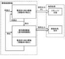
- FIG. 1 is a block diagram showing an example of a camera system 1 according to the present embodiment.
- the camera system 1 includes an imaging device 100, an illumination device 200, an image processing unit 300, and a system controller 400.
- camera system 1 ambient light and illumination light emitted by lighting device 200 are reflected by the subject, and the reflected light is converted into an electric charge by the photoelectric conversion unit of imaging device 100, and is extracted as an electrical signal and imaged.
- ambient light such as sunlight or external lighting is used for imaging
- camera system 1 does not need to be equipped with lighting device 200.
- the imaging device 100 includes an imaging element 110, a current change detection circuit 130, and a drive control circuit 140.
- the imaging element 110 has a photoelectric conversion unit 13, and outputs a signal based on light incident on the photoelectric conversion unit 13.
- the imaging element 110 also has a current measurement circuit 19 connected to the photoelectric conversion unit 13.
- the current measurement circuit 19 measures the current flowing in the photoelectric conversion unit 13. Note that at least some of the circuit elements of the current measurement circuit 19 may be provided outside the imaging element 110.
- the current change detection circuit 130 detects the change in the current measured by the current measurement circuit 19.
- the current change detection circuit 130 can detect the presence of a moving object, for example, based on the detected change in current.
- the drive control circuit 140 controls the operation of the imaging device 100 (mainly the imaging element 110).
- the current change detection circuit 130 and the drive control circuit 140 are each realized by one or more microcomputers or processors that incorporate programs for performing processing in the current change detection circuit 130 and the drive control circuit 140.
- the current change detection circuit 130 and the drive control circuit 140 may also be realized by individual microcomputers or processors, or may be realized by a single microcomputer or processor.
- the current change detection circuit 130 and the drive control circuit 140 may each include a dedicated logic circuit for performing processing in the current change detection circuit 130 and the drive control circuit 140. Details of the imaging device 100 will be described later.
- the lighting device 200 irradiates light containing, for example, near-infrared light as the lighting light.
- an electrical signal generated by photoelectric conversion in a photoelectric conversion section of the imaging device 100 that is sensitive to near-infrared wavelengths is extracted and imaged.
- the wavelength range of the near-infrared light contained in the lighting light is, for example, 680 nm or more and 3000 nm or less.
- the wavelength range of the near-infrared light contained in the lighting light may be 700 nm or more and 2000 nm or less, or 700 nm or more and 1600 nm or less.
- the lighting light does not have to contain near-infrared light, and may contain at least one of visible light and ultraviolet light.
- the type of light source used in the lighting device 200 is not particularly limited as long as it is a light source that can emit light of the desired wavelength.
- the light source used in the lighting device 200 is, for example, a halogen light source, an LED (Light Emitting Diode) light source, an organic EL (Electro Luminescence) light source, or a laser diode light source.
- the light source used in the lighting device 200 may be a combination of multiple light sources with different emission wavelengths.
- an inexpensive LED with a peak wavelength of 820 nm or more and 980 nm or less can be used as a light source that emits light including near-infrared rays.
- the image processing unit 300 is a processing circuit that performs various processes on output signals including image data output from the imaging device 100.
- the image processing unit 300 performs processes such as gamma correction, color interpolation, spatial interpolation, auto white balance, distance measurement calculation, and wavelength information separation.
- the image processing unit 300 processes the output signal from the imaging device 100 and outputs it to the outside as an image.
- the image processing unit 300 is realized by one or more microcomputers or processors that incorporate a program for performing the processing in the image processing unit 300.
- the image processing unit 300 may include a dedicated logic circuit for performing the processing in the image processing unit 300.
- a specific example of the image processing unit 300 is an ISP (Image Signal Processor).
- the system controller 400 controls the entire camera system 1. For example, the system controller 400 controls the timing of image capture by the image capture device 100 and the timing of illumination light irradiation by the illumination device 200.
- the system controller 400 is realized by one or more microcomputers or processors that incorporate a program for performing processing in the system controller 400.
- the system controller 400 may include a dedicated logic circuit for performing processing in the system controller 400.
- the imaging device 100, the lighting device 200, the image processing unit 300, and the system controller 400 are shown as separate functional blocks, but two or more of the imaging device 100, the lighting device 200, the image processing unit 300, and the system controller 400 may be integrated together by being provided in the same housing, etc. Also, the image processing unit 300 and the system controller 400 may each be realized by separate microcomputers or processors, etc., or may be realized by a single microcomputer or processor, etc.
- the functions of the image processing unit 300 and the system controller 400 may be possessed by the imaging device 100.
- at least one of the image processing unit 300 and the system controller 400 may be provided in the imaging device 100.
- the current change detection circuit 130, the drive control circuit 140, the image processing unit 300, and the system controller 400 may each be realized by an individual microcomputer or processor, etc., and two or more of these functions may be realized by a single microcomputer or processor, etc.
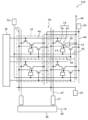
- FIG. 2 is a schematic diagram showing an exemplary circuit configuration of the image sensor 110 according to this embodiment. Note that the current measurement circuit 19 is omitted from FIG. 2. First, the configuration for capturing a normal image in the image sensor 110 will be described. Details of the current measurement circuit 19 will be described later.
- the imaging element 110 has a pixel array PA including a plurality of pixels 10 arranged two-dimensionally, and peripheral circuits having connections to each pixel 10.
- the peripheral circuits include, for example, a shield voltage supply circuit 18, a voltage supply circuit 32, a reset voltage source 34, a vertical scanning circuit 36, a column signal processing circuit 37, and a horizontal signal readout circuit 38.
- FIG. 2 shows a schematic example in which the pixels 10 are arranged in a matrix of two rows and two columns. The number and arrangement of the pixels 10 in the imaging element 110 are not limited to the example shown in FIG. 2.
- Each pixel 10 has a photoelectric conversion unit 13 and a signal detection circuit 14.
- the photoelectric conversion unit 13 has a photoelectric conversion layer sandwiched between two opposing electrodes, and receives incident light to generate a signal charge.
- the photoelectric conversion unit 13 does not need to be an independent element for each pixel 10 in its entirety, and for example, a portion of the photoelectric conversion unit 13 may span multiple pixels 10.
- the signal detection circuit 14 is a circuit that detects a pixel signal, which is an example of a signal based on the charge generated by the photoelectric conversion unit 13.
- the signal detection circuit 14 includes a signal detection transistor 24 and an address transistor 26.
- the signal detection transistor 24 and the address transistor 26 are, for example, field effect transistors (FETs), and here, an N-channel MOSFET (Metal Oxide Semiconductor Field Effect Transistor) is exemplified as the signal detection transistor 24 and the address transistor 26.
- Each transistor, such as the signal detection transistor 24, the address transistor 26, and the reset transistor 28 described later, has a control terminal, an input terminal, and an output terminal.
- the control terminal is, for example, a gate.
- the input terminal is one of the drain and the source, for example, the drain.
- the output terminal is the other of the drain and the source, for example, the source.
- the control terminal of the signal detection transistor 24 has an electrical connection with the photoelectric conversion unit 13.
- the signal charge generated by the photoelectric conversion unit 13 is stored in a charge storage region including a charge storage node 41 between the gate of the signal detection transistor 24 and the photoelectric conversion unit 13.
- the signal charge is holes and electrons.
- the charge storage node 41 is also called a "floating diffusion node.”
- the charge storage node 41 is an example of a charge storage unit. The charge is stored in the charge storage region including the charge storage node 41. The structure of the photoelectric conversion unit 13 will be described in detail later.
- the photoelectric conversion unit 13 of each pixel 10 is further connected to a sensitivity control line 42.
- the sensitivity control line 42 is connected to a voltage supply circuit 32.
- the voltage supply circuit 32 is an example of a first voltage supply circuit and is also called a sensitivity control voltage supply circuit.
- the voltage supply circuit 32 is a circuit configured to be able to supply at least two types of voltage. When the image sensor 110 is in operation, the voltage supply circuit 32 supplies a predetermined voltage to the photoelectric conversion unit 13, specifically to the counter electrode described later, via the sensitivity control line 42.
- the voltage supply circuit 32 is not limited to a specific power supply circuit, and may be a circuit that generates a predetermined voltage or a circuit that converts a voltage supplied from another power supply to a predetermined voltage. As will be described in detail later, the voltage supplied from the voltage supply circuit 32 to the photoelectric conversion unit 13 is switched between multiple different voltages, thereby controlling the start and end of the accumulation of signal charges from the photoelectric conversion unit 13 to the charge accumulation node 41. In other words, in this embodiment, the electronic shutter operation is performed by switching the voltage supplied from the voltage supply circuit 32 to the photoelectric conversion unit 13. An example of the operation of the image sensor 110 will be described later.
- the photoelectric conversion unit 13 of each pixel 10 is further connected to a shield line 17.
- the shield line 17 is connected to a shield voltage supply circuit 18.
- the shield voltage supply circuit 18 supplies a predetermined voltage to the photoelectric conversion unit 13, specifically, to a shield electrode described later, via the shield line 17.
- the shield voltage supply circuit 18 may be a circuit configured to be able to supply multiple voltages.
- the shield voltage supply circuit 18 is not limited to a specific power supply circuit, and may be a circuit that generates a predetermined voltage, or may be a circuit that converts a voltage supplied from another power supply into a predetermined voltage. Note that the image sensor 110 does not need to have the shield voltage supply circuit 18, and the shield voltage supply circuit 18 may be a circuit outside the image sensor 110.
- the shield line 17 may also be connected to ground instead of the shield voltage supply circuit 18.
- Each pixel 10 is connected to a power supply line 40 that supplies a power supply voltage VDD. As shown in FIG. 2, the power supply line 40 is connected to an input terminal of a signal detection transistor 24.
- the power supply line 40 functions as a source follower power supply, and the signal detection transistor 24 amplifies and outputs a signal corresponding to the charge generated by the photoelectric conversion unit 13.
- the input terminal of the address transistor 26 is connected to the output terminal of the signal detection transistor 24.
- the output terminal of the address transistor 26 is connected to one of a plurality of vertical signal lines 47 arranged for each column of the pixel array PA.
- the control terminal of the address transistor 26 is connected to an address control line 46, and by controlling the potential of the address control line 46, the output of the signal detection transistor 24 can be selectively read out to the corresponding vertical signal line 47.
- the address control line 46 is connected to the vertical scanning circuit 36.
- the vertical scanning circuit 36 is also called a "row scanning circuit.”
- the vertical scanning circuit 36 applies a predetermined voltage to the address control line 46, thereby selecting a plurality of pixels 10 arranged in each row on a row-by-row basis. This causes the signal of the selected pixel 10 to be read out, and the charge storage node 41 of the selected pixel 10 and the pixel electrode, which will be described later, to be reset.
- the vertical signal lines 47 are main signal lines that transmit pixel signals from the pixel array PA to the peripheral circuits.
- the column signal processing circuits 37 are connected to the vertical signal lines 47.
- the column signal processing circuits 37 are also called “row signal storage circuits”.
- the column signal processing circuits 37 perform noise suppression signal processing, such as correlated double sampling, and analog-to-digital conversion (AD conversion).
- AD conversion analog-to-digital conversion
- the column signal processing circuits 37 are provided corresponding to each column of pixels 10 in the pixel array PA.
- the horizontal signal readout circuits 38 are connected to these column signal processing circuits 37.
- the horizontal signal readout circuits 38 are also called “column scanning circuits”.
- the horizontal signal readout circuits 38 sequentially read out signals from the multiple column signal processing circuits 37 to the horizontal common signal lines 49.
- the pixel 10 has a reset transistor 28.
- the reset transistor 28 can be, for example, a field effect transistor, similar to the signal detection transistor 24 and the address transistor 26.
- an N-channel MOSFET is used as the reset transistor 28.
- the reset transistor 28 is connected between a reset voltage line 44 that supplies a reset voltage Vr and the charge storage node 41.
- the control terminal of the reset transistor 28 is connected to a reset control line 48, and the potential of the charge storage node 41 can be reset to the reset voltage Vr by controlling the potential of the reset control line 48.
- the reset control line 48 is connected to the vertical scanning circuit 36. Therefore, by the vertical scanning circuit 36 applying a predetermined voltage to the reset control line 48, it is possible to reset the multiple pixels 10 arranged in each row on a row-by-row basis.
- the reset voltage line 44 that supplies the reset voltage Vr to the reset transistor 28 is connected to the reset voltage source 34.
- the reset voltage source 34 is an example of a second voltage supply circuit and is also called a "reset voltage supply circuit.”
- the reset voltage source 34 is not limited to a specific power supply circuit as long as it has a configuration that can supply a predetermined reset voltage Vr to the reset voltage line 44 when the image sensor 110 is in operation, and is the same as the voltage supply circuit 32 and the shield voltage supply circuit 18 described above.
- Each of the voltage supply circuit 32, the shield voltage supply circuit 18, and the reset voltage source 34 may be a part of a single voltage supply circuit or may be an independent, separate voltage supply circuit.
- At least one of the voltage supply circuit 32, the shield voltage supply circuit 18, and the reset voltage source 34 may be a part of the vertical scanning circuit 36.
- at least one of the sensitivity control voltage from the voltage supply circuit 32, the shield voltage from the shield voltage supply circuit 18, and the reset voltage Vr from the reset voltage source 34 may be supplied to each pixel 10 via the vertical scanning circuit 36.
- the power supply voltage VDD of the signal detection circuit 14 is also possible to use the power supply voltage VDD of the signal detection circuit 14 as the reset voltage Vr.
- the voltage supply circuit (not shown in FIG. 2) that supplies a power supply voltage to each pixel 10 and the reset voltage source 34 can be made common.
- the power supply line 40 and the reset voltage line 44 can be made common, the wiring in the pixel array PA can be simplified.
- using different voltages for the reset voltage Vr and the power supply voltage VDD of the signal detection circuit 14 allows for more flexible control of the image sensor 110.
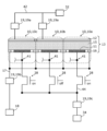
- FIG. 3 is a cross-sectional view showing a schematic diagram of an exemplary device structure of a pixel 10 according to the present embodiment.
- the above-mentioned signal detection transistor 24, address transistor 26, and reset transistor 28 are formed on a semiconductor substrate 20.
- the semiconductor substrate 20 is not limited to a substrate made entirely of semiconductor material.
- the semiconductor substrate 20 may be an insulating substrate having a semiconductor layer provided on the surface on which the photosensitive region is formed.
- a P-type silicon (Si) substrate is used as the semiconductor substrate 20.
- the semiconductor substrate 20 has impurity regions 26s, 24s, 24d, 28d, and 28s, and an element isolation region 20t for electrical isolation between the pixels 10.
- the impurity regions 26s, 24s, 24d, 28d, and 28s are N-type regions.
- the element isolation region 20t is also provided between the impurity region 24d and the impurity region 28d.
- the element isolation region 20t is formed, for example, by ion implantation of an acceptor under predetermined implantation conditions.
- the impurity regions 26s, 24s, 24d, 28d, and 28s are, for example, diffusion layers formed in the semiconductor substrate 20.
- the signal detection transistor 24 includes impurity regions 24s and 24d and a gate electrode 24g.
- the impurity region 24s functions, for example, as a source region of the signal detection transistor 24.
- the impurity region 24d functions, for example, as a drain region of the signal detection transistor 24.
- the channel region of the signal detection transistor 24 is formed between the impurity region 24s and the impurity region 24d.
- the address transistor 26 includes impurity regions 26s and 24s, and a gate electrode 26g connected to an address control line 46 (see FIG. 2).
- the signal detection transistor 24 and the address transistor 26 are electrically connected to each other by sharing the impurity region 24s.
- the impurity region 26s functions as, for example, a source region of the address transistor 26.
- the impurity region 26s is connected to a vertical signal line 47 (see FIG. 2), not shown in FIG. 3.
- the gate electrodes 24g, 26g, and 28g are each formed using a conductive material.
- the conductive material is, for example, polysilicon that has been doped with impurities to make it conductive, but may also be a metal material.
- An interlayer insulating layer 50 is disposed on the semiconductor substrate 20 so as to cover the signal detection transistor 24, the address transistor 26, and the reset transistor 28.
- the interlayer insulating layer 50 is formed of an insulating material such as silicon oxide.
- a wiring layer 56 may be disposed in the interlayer insulating layer 50.
- the wiring layer 56 is formed of a metal such as copper.
- the wiring layer 56 may include, for example, wiring such as the vertical signal line 47 described above as part of it.
- the number of insulating layers in the interlayer insulating layer 50 and the number of layers included in the wiring layer 56 disposed in the interlayer insulating layer 50 can be set arbitrarily and are not limited to the example shown in FIG. 3.
- the above-mentioned photoelectric conversion unit 13 is disposed on the interlayer insulating layer 50.
- a plurality of pixels 10 constituting a pixel array PA are formed on a semiconductor substrate 20.
- a plurality of pixels 10 arranged two-dimensionally on the semiconductor substrate 20 form a pixel region, which is a photosensitive region.
- the distance between two adjacent pixels 10 can be, for example, approximately 2 ⁇ m.
- the distance between two adjacent pixels 10 is also called the "pixel pitch.”
- the photoelectric conversion unit 13 includes a pixel electrode 11, a counter electrode 12, and a photoelectric conversion layer 15 disposed therebetween.
- the photoelectric conversion unit 13 further includes a shield electrode 16.
- the pixel electrode 11 is an example of a first electrode
- the counter electrode 12 is an example of a second electrode
- the shield electrode 16 is an example of a third electrode.
- the counter electrode 12, the photoelectric conversion layer 15, and the shield electrode 16 are formed across multiple pixels 10.
- the pixel electrode 11 is provided for each pixel 10, and is electrically isolated from the pixel electrodes 11 of the other pixels 10 by being spatially separated from the pixel electrodes 11 of the other adjacent pixels 10.
- the counter electrode 12 is disposed opposite the pixel electrode 11 with the photoelectric conversion layer 15 interposed therebetween.
- the counter electrode 12 is, for example, a transparent electrode formed from a transparent conductive material.
- the counter electrode 12 is disposed on the side of the photoelectric conversion layer 15 where light is incident. Therefore, light transmitted through the counter electrode 12 is incident on the photoelectric conversion layer 15.
- the light detected by the image sensor 110 is not limited to light within the wavelength range of visible light (e.g., 380 nm or more and 780 nm or less).
- transparent means that at least a part of the light in the wavelength range to be detected is transmitted, and it is not essential that light is transmitted over the entire wavelength range of visible light.
- the counter electrode 12 can be made of a transparent conducting oxide (TCO) such as ITO, IZO, AZO, FTO, SnO 2 , TiO 2 , or ZnO 2 .
- TCO transparent conducting oxide
- the photoelectric conversion layer 15 receives incident light and generates hole-electron pairs, which are pairs of electric charges.
- the photoelectric conversion layer 15 is formed, for example, from an organic material. Specific examples of materials that make up the photoelectric conversion layer 15 will be described later.
- the counter electrode 12 is connected to the sensitivity control line 42 connected to the voltage supply circuit 32.
- the counter electrode 12 is formed across a plurality of pixels 10. Therefore, it is possible to apply a sensitivity control voltage of a desired magnitude from the voltage supply circuit 32 to a plurality of pixels 10 at once through the sensitivity control line 42. If a sensitivity control voltage of a desired magnitude can be applied from the voltage supply circuit 32, the counter electrode 12 may be provided separately for each pixel 10, or may be provided separately for each pixel block consisting of two or more pixels 10, which is a part of the plurality of pixels 10. In other words, the counter electrode 12 may be divided into a plurality of parts. In the example shown in FIG.
- the sensitivity control line 42 connected to the counter electrode 12 is connected to one voltage supply circuit 32, but this is not limited to this.
- a corresponding voltage supply circuit 32 out of the plurality of voltage supply circuits 32 may be connected to each of the plurality of parts of the counter electrode 12 through the sensitivity control line 42.
- the photoelectric conversion layer 15 may be provided separately for each pixel 10, or may be provided separately for each pixel block consisting of two or more pixels 10 that are a portion of the multiple pixels 10. In other words, the photoelectric conversion layer 15 may be divided into multiple parts.
- the voltage supply circuit 32 applies a voltage between the pixel electrode 11 and the counter electrode 12 by supplying a voltage to the counter electrode 12. As will be described in detail later, the voltage supply circuit 32 supplies different voltages to the counter electrode 12 between an exposure period and a non-exposure period, for example.
- the "exposure period” refers to a period during which signal charge, which is one of the positive and negative charges generated by photoelectric conversion, is accumulated in a charge accumulation region, and may also be called the "charge accumulation period.”
- non-exposure period a period other than an exposure period during operation of the imaging device is referred to as a "non-exposure period.”
- the “non-exposure period” is not limited to a period during which light is blocked from entering the photoelectric conversion unit 13, but may also include a period during which light is irradiated onto the photoelectric conversion unit 13.
- the “non-exposure period” also includes a period during which signal charge is unintentionally accumulated in the charge accumulation region due to the occurrence of parasitic sensitivity.
- the pixel electrode 11 can collect either the holes or the electrons of the hole-electron pairs generated in the photoelectric conversion layer 15 by photoelectric conversion.
- the voltage applied between the pixel electrode 11 and the counter electrode 12 is also called the "bias voltage”.
- the signal charge collected by the pixel electrode 11 is stored in the charge accumulation region. For example, when holes are used as signal charges, it is possible to selectively collect holes by the pixel electrode 11 by making the potential of the counter electrode 12 higher than that of the pixel electrode 11.
- the counter electrode 12 is connected to the above-mentioned sensitivity control line 42, for example, in the peripheral region of the pixel array PA, and a voltage is supplied from the voltage supply circuit 32. Note that the counter electrode 12 may also be supplied with a voltage from the voltage supply circuit 32 via a via contact penetrating the photoelectric conversion layer 15 and the wiring layer 56.
- the pixel electrode 11 facing the counter electrode 12 collects one of the positive and negative charges generated by photoelectric conversion in the photoelectric conversion layer 15 by applying an appropriate bias voltage between the counter electrode 12 and the pixel electrode 11 as described above.
- the pixel electrode 11 is made of, for example, a metal such as aluminum or copper, a metal nitride, or polysilicon that has been doped with impurities to give it conductivity.
- the pixel electrode 11 may be a light-shielding electrode.
- a TaN electrode with a thickness of 100 nm as the pixel electrode 11, sufficient light-shielding properties can be achieved.
- a light-shielding film may be formed in the interlayer insulating layer 50 using the above-mentioned wiring layer 56.
- the pixel electrode 11 is connected to the gate electrode 24g of the signal detection transistor 24 via the plug 52, the wiring 53, and the contact plug 54.
- the gate of the signal detection transistor 24 has an electrical connection with the pixel electrode 11.
- the plug 52 and the wiring 53 are made of a metal such as copper.
- the plug 52, the wiring 53, and the contact plug 54 constitute at least a part of the charge storage node 41 (see FIG. 2) between the signal detection transistor 24 and the photoelectric conversion unit 13.
- the wiring 53 may be a part of the wiring layer 56.
- the pixel electrode 11 is also connected to the impurity region 28d via the plug 52, the wiring 53, and the contact plug 55. In the configuration illustrated in FIG.
- the gate electrode 24g of the signal detection transistor 24, the plug 52, the wiring 53, the contact plugs 54 and 55, and the impurity region 28d, which is one of the source region and the drain region of the reset transistor 28, function as a charge storage region that stores the signal charge collected by the pixel electrode 11.
- a voltage corresponding to the amount of signal charge accumulated in the charge accumulation region is applied to the gate of the signal detection transistor 24.
- the voltage applied to the gate of the signal detection transistor 24 corresponds to the potential of the charge accumulation node 41.
- the signal detection transistor 24 amplifies this voltage.
- the voltage amplified by the signal detection transistor 24 is selectively read out as a signal voltage via the address transistor 26.
- the shield electrode 16 is disposed opposite the counter electrode 12 with the photoelectric conversion layer 15 sandwiched therebetween. Although not shown in FIG. 3, as described above, the shield electrode 16 is connected to the shield wire 17, and a voltage is applied from the shield voltage supply circuit 18 via the shield wire 17. A portion of the shield wire 17 may be included in the wiring layer 56. Although not shown in FIG. 3, the shield electrode 16 may be connected to the wiring layer 56 via a contact or the like.
- FIG. 4 is a plan view showing an example of a planar layout of the pixel electrode 11 and the shield electrode 16. Note that in FIG. 4, illustrations other than the pixel electrode 11 and the shield electrode 16 are omitted. Also, in FIG. 4, for ease of viewing, the pixel electrode 11 and the shield electrode 16 are shaded in the same way as the pixel electrode 11 and the shield electrode 16 shown in the cross section of FIG. 3.
- the pixel electrodes 11 are arranged, for example, in an array.
- the shield electrodes 16 are disposed between adjacent pixel electrodes 11 in a planar view.
- the shield electrodes 16 surround the pixel electrodes 11 in a planar view.
- the shield electrodes 16 are disposed in a lattice shape in a planar view, and a pixel electrode 11 is disposed within each lattice.
- the shield electrodes 16 are formed, for example, collectively across multiple pixels 10, and all pixels 10 have the same potential.
- the shield electrode 16 may be provided separately for each pixel 10, or for each pixel block consisting of two or more pixels 10 that are a part of the multiple pixels 10. In other words, the shield electrode 16 may be divided into multiple parts. In the example shown in FIG. 2, the shield wire 17 connected to the shield electrode 16 is connected to one shield voltage supply circuit 18, but this is not limited to this. When the shield electrode 16 is divided into multiple parts, each of the multiple parts of the shield electrode 16 may be connected to a corresponding one of the multiple shield voltage supply circuits 18 via the shield wire 17.
- the voltage applied to the shield electrode 16 can be used to suppress the movement of signal charges between pixels 10, that is, so-called crosstalk. Therefore, color mixing can be suppressed even if the photoelectric conversion layer 15 is not physically separated.
- the voltage applied to the shield electrode 16 is set, for example, so that the potential of the shield electrode 16 is higher than the potential of the pixel electrode 11. For example, a voltage higher than the reset voltage Vr is applied to the shield electrode 16. This makes it easier for holes to move to the pixel electrodes 11 surrounded by the shield electrode 16 in a planar view, and it is possible to suppress the movement of holes beyond the shield electrode 16 to the pixel electrode 11 of the adjacent pixel 10.
- the voltage applied to the shield electrode 16 may be set so that the potential of the shield electrode 16 is lower than the potential of the pixel electrode 11.
- a voltage lower than the reset voltage Vr is applied to the shield electrode 16.
- the shield electrode 16 is formed, for example, from a metal such as aluminum or copper, a metal nitride, or polysilicon that has been doped with impurities to make it conductive.
- the shield electrode 16 may be a light-shielding electrode.
- the shield electrode 16 may be formed from the same material as the pixel electrode 11.
- the shield electrode 16 and the pixel electrode 11 may be formed simultaneously in the same process.
- At least one of the circuits of the peripheral circuits of the image sensor 110 described above, the current change detection circuit 130, and the drive control circuit 140 may be formed on the same semiconductor substrate 20 as the image sensor 110.
- the photoelectric conversion layer 15 As described above, by irradiating the photoelectric conversion layer 15 with light and applying a bias voltage between the pixel electrode 11 and the counter electrode 12, one of the positive and negative charges generated by photoelectric conversion can be collected by the pixel electrode 11, and the collected charges can be stored in the charge accumulation region.
- a photoelectric conversion unit 13 having a photoelectric conversion layer 15 that exhibits the photocurrent characteristics described below, and by reducing the potential difference between the pixel electrode 11 and the counter electrode 12 to a certain extent, it is possible to suppress the signal charge already accumulated in the charge accumulation region from moving to the counter electrode 12 via the photoelectric conversion layer 15. Furthermore, it is possible to suppress further accumulation of signal charge in the charge accumulation region after reducing the potential difference.
- a global shutter function can be realized without providing a separate element such as a transfer transistor in each of the multiple pixels 10 as in the technology described in Patent Document 1.
- An example of the operation of the imaging device 100 will be described later.
- normal rolling shutter drive is also possible by keeping the magnitude of the bias voltage applied to the photoelectric conversion unit 13 constant and setting the completion of resetting the pixel 10 as the start of the exposure period.
- the photoelectric conversion layer 15 includes, for example, a semiconductor material.
- a semiconductor material for example, an organic semiconductor material is used as the semiconductor material.
- the photoelectric conversion layer 15 contains, for example, tin phthalocyanine represented by the following general formula (1).
- tin phthalocyanine represented by the following general formula (1) may be simply referred to as "tin phthalocyanine”.
- R 1 to R 24 each independently represent a hydrogen atom or a substituent.
- the substituent is not limited to a specific substituent.
- the substituent may be a deuterium atom, a halogen atom, an alkyl group (including a cycloalkyl group, a bicycloalkyl group, and a tricycloalkyl group), an alkenyl group (including a cycloalkenyl group and a bicycloalkenyl group), an alkynyl group, an aryl group, a heterocyclic group (which may also be called a heterocyclic group), a cyano group, a hydroxy group, a nitro group, a carboxy group, an alkoxy group, an aryloxy group, a silyloxy group, a heterocyclic oxy group, an acyloxy group, a carbamoyloxy group, an alkoxycarbonyloxy group, an aryloxycarbonyloxy group, an amino
- the substituent may be an amino group, an aryloxycarbonylamino group, a sulfamoylamino group, an alkylsulfonylamino group, an arylsulfonylamino group, a mercapto group, an alkylthio group, an arylthio group, a heterocyclic thio group, a sulfamoyl group, a sulfo group, an alkylsulfinyl group, an arylsulfinyl group, an alkylsulfonyl group, an arylsulfonyl group, an acyl group, an aryloxycarbonyl group, an alkoxycarbonyl group, a carbamoyl group, an arylazo group, a heterocyclic azo group, an imido group, a phosphino group, a phosphinyl group, a phosphinyloxy group, a
- the tin phthalocyanine represented by the above general formula (1) a commercially available product can be used.
- the tin phthalocyanine represented by the above general formula (1) can be synthesized from a naphthalene derivative represented by the following general formula (2) as a starting material, as shown in, for example, Patent Document 3.
- R 25 to R 30 in the general formula (2) can be the same substituents as R 1 to R 24 in the general formula (1).
- R1 to R24 may be hydrogen atoms or deuterium atoms, 16 or more of R1 to R24 may be hydrogen atoms or deuterium atoms, or all may be hydrogen atoms or deuterium atoms.
- the tin phthalocyanine represented by the following formula (3) is advantageous from the viewpoint of ease of synthesis.
- Tin phthalocyanine represented by the above general formula (1) has absorption in the wavelength range of approximately 200 nm or more and 1100 nm or less.
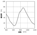
- tin phthalocyanine represented by the above formula (3) has an absorption peak at a wavelength of approximately 870 nm, as shown in Figure 5.
- Figure 5 shows an example of the absorption spectrum of a photoelectric conversion layer containing tin phthalocyanine represented by the above formula (3). Note that the absorption spectrum was measured using a sample in which a photoelectric conversion layer with a thickness of 30 nm was laminated on a quartz substrate.
- a photoelectric conversion layer formed from a material containing tin naphthalocyanine has absorption in the visible light wavelength region and the near infrared wavelength region.
- a material containing tin naphthalocyanine as the material constituting the photoelectric conversion layer 15, for example, an optical sensor capable of detecting near infrared light can be realized.
- a naphthalocyanine derivative in which the central metal is not tin but another metal such as silicon or germanium may be used.
- an axial ligand may be coordinated to the central metal of the naphthalocyanine derivative.
- FIG. 6 is a cross-sectional view showing a schematic example of the configuration of the photoelectric conversion layer 15.
- the photoelectric conversion layer 15 has a hole blocking layer 15h, a photoelectric conversion structure 15A, and an electron blocking layer 15e.
- the hole blocking layer 15h is disposed between the photoelectric conversion structure 15A and the counter electrode 12, and the electron blocking layer 15e is disposed between the photoelectric conversion structure 15A and the pixel electrode 11.
- the photoelectric conversion layer 15 does not have to have at least one of the hole blocking layer 15h and the electron blocking layer 15e.
- the photoelectric conversion structure 15A shown in FIG. 6 includes, for example, at least one of a p-type semiconductor and an n-type semiconductor.
- the photoelectric conversion structure 15A has a p-type semiconductor layer 150p, an n-type semiconductor layer 150n, and a mixed layer 150m sandwiched between the p-type semiconductor layer 150p and the n-type semiconductor layer 150n.
- the p-type semiconductor layer 150p is disposed between the electron blocking layer 15e and the mixed layer 150m, and has a function of photoelectric conversion and/or hole transport.
- the n-type semiconductor layer 150n is disposed between the hole blocking layer 15h and the mixed layer 150m, and has a function of photoelectric conversion and/or electron transport.
- the mixed layer 150m may include at least one of a p-type semiconductor and an n-type semiconductor.
- the p-type semiconductor layer 150p contains an organic p-type semiconductor
- the n-type semiconductor layer 150n contains an organic n-type semiconductor. That is, the photoelectric conversion structure 15A contains an organic photoelectric conversion material containing tin phthalocyanine represented by the above-mentioned general formula (1), an organic p-type semiconductor, and an organic n-type semiconductor.
- An organic p-type semiconductor is a donor organic semiconductor, and is mainly represented by a hole-transporting organic compound, and refers to an organic compound that has the property of easily donating electrons. More specifically, an organic p-type semiconductor is a donor organic compound, and refers to the organic compound that has the smaller ionization potential when two organic materials are used in contact. Therefore, any organic compound that has electron-donating properties can be used as a donor organic compound.
- donor organic compounds include triarylamine compounds, benzidine compounds, pyrazoline compounds, styrylamine compounds, hydrazone compounds, triphenylmethane compounds, carbazole compounds, polysilane compounds, thiophene compounds, phthalocyanine compounds, naphthalocyanine compounds, subphthalocyanine compounds, cyanine compounds, merocyanine compounds, oxonol compounds, polyamine compounds, indole compounds, pyrrole compounds, pyrazole compounds, polyarylene compounds, condensed aromatic carbon ring compounds (naphthalene derivatives, anthracene derivatives, phenanthrene derivatives, tetracene derivatives, pyrene derivatives, perylene derivatives, fluoranthene derivatives), and metal complexes having nitrogen-containing heterocyclic compounds as ligands.
- the donor organic semiconductor is not limited to these, and any organic compound having a smaller ionization potential than the organic compound used as the acceptor organic semiconductor described later can be used as the donor organic semiconductor.
- the above-mentioned tin naphthalocyanine is an example of an organic p-type semiconductor material.
- Organic n-type semiconductors are acceptor organic semiconductors, and are mainly represented by electron transporting organic compounds, and refer to organic compounds that have the property of readily accepting electrons. More specifically, organic n-type semiconductors are acceptor organic compounds, and refer to the organic compound that has the greater electron affinity when two organic compounds are used in contact. Therefore, any organic compound that has electron accepting properties can be used as an acceptor organic compound.
- acceptor organic compound examples include fullerene, fullerene derivatives, condensed aromatic carbon ring compounds (naphthalene derivatives, anthracene derivatives, phenanthrene derivatives, tetracene derivatives, pyrene derivatives, perylene derivatives, and fluoranthene derivatives), 5- to 7-membered heterocyclic compounds containing a nitrogen atom, an oxygen atom, or a sulfur atom (e.g., pyridine, pyrazine, pyrimidine, pyridazine, triazine, quinoline, quinoxaline, quinazoline, phthalazine, cinnoline, isoquinoline, pteridine, acridine, phenazine, phenanthroline, tetrazole, pyrazoline, and the like).
- condensed aromatic carbon ring compounds e.g., pyridine, pyrazine, pyrimidine, pyridazin
- organic semiconductor examples include metal complexes having a ligand such as aryl, imidazole, thiazole, oxazole, indazole, benzimidazole, benzotriazole, benzoxazole, benzothiazole, carbazole, purine, triazolopyridazine, triazolopyrimidine, tetrazaindene, oxadiazole, imidazopyridine, pyrrolidine, pyrrolopyridine, thiadiazolopyridine, dibenzazepine, tribenzazepine, etc.), polyarylene compounds, fluorene compounds, cyclopentadiene compounds, silyl compounds, and nitrogen-containing heterocyclic compounds.
- the organic semiconductor can be any organic compound that has a larger electron affinity than the organic compound used as the donor organic compound, as described above.
- the mixed layer 150m may be, for example, a bulk heterojunction structure layer including a p-type semiconductor and an n-type semiconductor.
- tin phthalocyanine represented by the above general formula (1) may be used as the p-type semiconductor material.
- n-type semiconductor material for example, fullerene and/or a fullerene derivative may be used.
- the material constituting the p-type semiconductor layer 150p may be the same as the p-type semiconductor material contained in the mixed layer 150m.
- the material constituting the n-type semiconductor layer 150n may be the same as the n-type semiconductor material contained in the mixed layer 150m.
- Patent Document 4 Japanese Patent No. 5553727.
- Japanese Patent No. 5553727 the entire disclosure of Japanese Patent No. 5553727 is incorporated herein by reference.
- the photoelectric conversion layer 15 that uses tin phthalocyanine and is sensitive to near-infrared light has been described, but the material contained in the photoelectric conversion layer 15 is not limited to photoelectric conversion materials that are sensitive to near-infrared light.
- the photoelectric conversion layer 15 can become a photoelectric conversion layer 15 that is sensitive to visible light by using subphthalocyanine as a p-type semiconductor and fullerene and/or a fullerene derivative as an n-type semiconductor.
- FIG. 7 is a diagram showing exemplary photocurrent characteristics of the photoelectric conversion unit 13.
- the solid line graph shows exemplary current-voltage characteristics (I-V characteristics) of the photoelectric conversion unit 13 when it is irradiated with light, i.e., when it is bright.
- FIG. 7 also shows, by a dashed line, an example of the I-V characteristics of the photoelectric conversion unit 13 when it is not irradiated with light, i.e., when it is dark.
- Figure 7 shows the change in current density between the main surfaces of the photoelectric conversion layer 15 when the bias voltage applied between the pixel electrode 11 and the counter electrode 12 of the photoelectric conversion unit 13 is changed under a constant illuminance.
- the forward and reverse directions of the bias voltage are defined as follows.
- the bias voltage that makes the potential of the p-type semiconductor layer higher than that of the n-type semiconductor layer is defined as the forward bias voltage.
- the bias voltage that makes the potential of the p-type semiconductor layer lower than that of the n-type semiconductor layer is defined as the reverse bias voltage.
- a bias voltage that makes the potential of the main surface side where more p-type semiconductors than n-type semiconductors appear is higher than the potential of the main surface side where more n-type semiconductors than p-type semiconductors appear is defined as a forward bias voltage.
- a voltage that makes the potential of the counter electrode 12 higher than the potential of the pixel electrode 11 is a reverse bias voltage
- a voltage that makes the potential of the counter electrode 12 lower than the potential of the pixel electrode 11 is a forward bias voltage
- the photocurrent characteristics of the photoelectric conversion unit 13 are roughly characterized by three voltage ranges, from the first voltage range to the third voltage range.
- the first voltage range is a reverse bias voltage range, and is a voltage range in which the absolute value of the output current density increases as the reverse bias voltage increases.
- the first voltage range can be said to be a voltage range in which the photocurrent increases as the bias voltage applied between the pixel electrode 11 and the counter electrode 12 increases.
- the second voltage range is a forward bias voltage range, and is a voltage range in which the output current density increases as the forward bias voltage increases. In other words, the second voltage range is a voltage range in which the photocurrent in the opposite direction to the first voltage range increases as the bias voltage applied between the pixel electrode 11 and the counter electrode 12 increases.
- the third voltage range is a voltage range between the first voltage range and the second voltage range.
- the first to third voltage ranges can also be distinguished by the slope of the graph of the photocurrent characteristics when linear vertical and horizontal axes are used.
- the average slopes of the graphs in the first and second voltage ranges are shown by dashed and dotted lines L1 and L2, respectively.
- the rates of change of the output current density with respect to an increase in the bias voltage in the first, second, and third voltage ranges are different from each other.
- the third voltage range is also defined as a voltage range in which the rate of change of the output current density with respect to the bias voltage is smaller than the rate of change in the first voltage range and the rate of change in the second voltage range.
- the third voltage range may be determined based on the position of the rise or fall in the graph showing the IV characteristics.
- the third voltage range is, for example, larger than -1V and smaller than +1V.
- the absolute value of the current density is, for example, 100 ⁇ A/cm 2 or less.
- the difference between the dark current and the light current in the third voltage range is smaller than the difference between the dark current and the light current in the first voltage range and the difference between the dark current and the light current in the second voltage range.
- the dark current is the current that flows through the photoelectric conversion layer 15 when no light is irradiated
- the light current is the current that flows through the photoelectric conversion layer 15 when light is irradiated.
- I-V characteristics of the photoelectric conversion unit 13 shown in FIG. 7 are just an example, and the desired I-V characteristics can be achieved by adjusting the configuration and materials of the photoelectric conversion layer 15 described above.
- FIG. 8 is a diagram for explaining an example of the operation of normal imaging drive in the imaging device 100 according to this embodiment.
- FIG. 8 shows the timing of the falling or rising edge of the synchronization signal, the change over time in the magnitude of the bias voltage applied to the photoelectric conversion unit 13, and the timing of reset and exposure in each row of the pixel array PA (see FIG. 2).
- the top graph (a) in FIG. 8 shows the timing of the fall or rise of the vertical synchronization signal Vss.
- Graph (b) in FIG. 8 shows the timing of the fall or rise of the horizontal synchronization signal Hss.
- Graph (c) in FIG. 8 shows an example of the change over time of the voltage Vb applied to the counter electrode 12 from the voltage supply circuit 32 via the sensitivity control line 42.
- Graph (d) in FIG. 8 shows the change over time of the potential ⁇ of the counter electrode 12, that is, the bias voltage, when the potential of the pixel electrode 11 is used as a reference.
- the double-headed arrow G3 in the graph (d) of the potential ⁇ in FIG. 8 indicates the third voltage range described above.
- Chart (e) in FIG. 8 shows the timing of reset and exposure in each row of the pixel array PA.
- the charge storage region of each pixel 10 in the pixel array PA is reset, and the pixel signal after reset is read out. For example, as shown in FIG. 8, resetting of multiple pixels 10 belonging to row R0 is started (time t0) based on the vertical synchronization signal Vss. Note that the rectangle with low-density halftone dots in chart (e) of FIG. 8 shows a schematic representation of the signal readout period. This readout period may include a reset period for resetting the potential of the charge storage region of the pixel 10 as part of it.
- the address transistor 26 whose gate is connected to the address control line 46 of the R0th row is turned ON by controlling the potential of the address control line 46 of the R0th row, and further, the reset transistor 28 whose gate is connected to the reset control line 48 of the R0th row is turned ON by controlling the potential of the reset control line 48 of the R0th row.
- This connects the charge storage node 41 and the reset voltage line 44, and the reset voltage Vr is supplied to the charge storage region. That is, the potentials of the charge storage node 41, the gate electrode 24g of the signal detection transistor 24, and the pixel electrode 11 of the photoelectric conversion unit 13 are reset to the reset voltage Vr.
- a pixel signal corresponding to the potential of the charge storage region after reset is read out from the pixel 10 of the R0th row via the vertical signal line 47.
- the pixel signal obtained at this time is a pixel signal corresponding to the magnitude of the reset voltage Vr.
- the reset transistor 28 and the address transistor 26 are turned OFF.
- the pixel signal may be read out before resetting.
- resetting of the pixels 10 in each row from row R0 to row R7 is performed sequentially row by row in accordance with the horizontal synchronization signal Hss.
- the interval between pulses of the horizontal synchronization signal Hss in other words, the period from when a row is selected to when the next row is selected, may be referred to as the "1H period.”
- the period from time t0 to time t1 corresponds to the 1H period.
- a voltage V3 is applied from the voltage supply circuit 32 to the counter electrode 12 so that the voltage applied between the pixel electrode 11 and the counter electrode 12 is within the above-mentioned third voltage range.
- a bias voltage within the third voltage range is applied between the pixel electrode 11 and the counter electrode 12.
- the period indicated by a rectangle with low density halftone dots and a rectangle with high density halftone dots represents the non-exposure period.
- a bias voltage within the third voltage range is applied between the pixel electrode 11 and the counter electrode 12 during the non-exposure period.
- the voltage V3 for applying the bias voltage within the third voltage range between the pixel electrode 11 and the counter electrode 12 is not limited to 0 V.
- the voltage V3 is set, for example, in response to the reset voltage Vr so that the bias voltage is a voltage within the third voltage range.
- an exposure period is started based on the horizontal synchronization signal Hss (time t9).
- the white rectangles represent the exposure period in each row.
- the exposure period is started by the voltage supply circuit 32 switching the voltage applied to the counter electrode 12 to a voltage Ve different from the voltage V3.
- the voltage Ve is, for example, a voltage such that the bias voltage applied between the pixel electrode 11 and the counter electrode 12 falls within the above-mentioned first voltage range, for example, about 10 V.
- the signal charges in the photoelectric conversion layer 15, in this example, holes are collected by the pixel electrode 11 and stored in a charge storage region including the charge storage node 41.
- the voltage Ve is set, for example, according to the reset voltage Vr so that the bias voltage falls within the first voltage range.
- the voltage supply circuit 32 switches the voltage applied to the counter electrode 12 back to voltage V3, thereby ending the exposure period (time t13).
- the voltage applied to the counter electrode 12 is switched between voltage V3 and voltage Ve, thereby switching between exposure and non-exposure periods.
- the start (time t9) and end (time t13) of the exposure period in this example are common to all pixels 10 included in the pixel array PA.
- the operation described here is an example in which the global shutter method is applied to the imaging element 110, and the imaging device 100 is driven by the global shutter method in which the exposure period is determined by changing the voltage applied by the voltage supply circuit 32 between the pixel electrode 11 and the counter electrode 12.
- pixel signals are read out from the pixels 10 belonging to each row of the pixel array PA.
- signal charges are read out from the pixels 10 belonging to each row from row R0 to row R7 in sequence, row by row.
- the period from when a pixel 10 belonging to a certain row is selected to when a pixel 10 belonging to that row is selected again may be referred to as the "1V period.”
- the period from time t0 to time t15 corresponds to the 1V period.
- the 1V period is, for example, one frame period.
- the address transistor 26 of row R0 When the exposure period ends and pixel signals are read from pixels 10 belonging to row R0 starting at time t15, the address transistor 26 of row R0 is first turned ON. This causes a pixel signal corresponding to the amount of charge accumulated in the charge accumulation region during the exposure period, i.e., the potential of the charge accumulation region after the exposure period, to be output to the vertical signal line 47. Following the reading of the pixel signal, the reset transistor 28 may be turned ON to reset the pixel 10. If necessary, the pixel signal may also be read after this reset. After the pixel signal is read, the address transistor 26 is turned OFF, and if the pixel 10 is reset, the reset transistor 28 is also turned OFF.
- a signal from which fixed noise has been removed is obtained by taking the difference between the pixel signals after reset read between time t0 and time t9.
- This removal of fixed noise is performed, for example, by the column signal processing circuit 37.
- the removal of fixed noise may be performed before or after AD conversion of the pixel signals.
- a signal is read from the column signal processing circuit 37 by the horizontal signal readout circuit 38, and is processed by a signal processing circuit (not shown) or the like as necessary, and output to the outside of the imaging device 100.
- a signal from which fixed noise has been removed may be obtained by taking the difference between the pixel signal read after the reset and the pixel signal read before the reset.
- the voltage applied to the counter electrode 12 is changed back to voltage V3, so that the photoelectric conversion unit 13 after the accumulation of signal charge in the charge accumulation region is in a state in which a bias voltage within the third voltage range is applied.
- a bias voltage within the third voltage range it is possible to suppress the movement of signal charge already accumulated in the charge accumulation region to the counter electrode 12 via the photoelectric conversion layer 15.
- by applying a bias voltage within the third voltage range to the photoelectric conversion unit 13 it is possible to hold the signal charge accumulated during the exposure period in the charge accumulation region. In other words, it is possible to suppress the occurrence of negative parasitic sensitivity caused by the loss of signal charge from the charge accumulation region.
- the start and end of the exposure period are controlled by the voltage Vb applied to the opposing electrode 12. That is, according to this embodiment, a global shutter function can be realized without providing a transfer transistor or the like in each pixel 10.
- the electronic shutter is executed by controlling the voltage Vb without transferring signal charge via a transfer transistor, allowing for faster operation.
- this is also advantageous for miniaturizing pixels.
- the imaging device 100 may be driven by the rolling shutter method in normal imaging drive.
- the voltage applied to the opposing electrode 12 is constant at voltage Ve.
- the end of the reset operation marks the start of the exposure period
- the start of the subsequent readout operation marks the end of the exposure period.
- the exposure period of the pixel 10 belonging to row R0 is from time t1 to time t15.
- the current measurement circuit 19 that measures the current flowing in the photoelectric conversion unit 13.
- the current change detection circuit 130 detects a change in the current flowing in the photoelectric conversion unit 13 measured by the current measurement circuit 19, and it is possible to detect a moving object based on the detected change in current.
- the current measurement circuit 19 is disposed on the wiring connected to the photoelectric conversion unit 13, and measures the current flowing through the photoelectric conversion unit 13.
- the photoelectric conversion unit 13 has the counter electrode 12, the shield electrode 16, and the pixel electrode 11 as electrodes connected to the wiring, and therefore the current measurement circuits 19a, 19b, and 19c are connected to any of these electrodes.
- the current measurement circuit 19a is an example of a first current measurement circuit, and is a current measurement circuit connected to the counter electrode 12.
- the current measurement circuit 19b is an example of a second current measurement circuit, and is a current measurement circuit connected to the shield electrode 16.
- the current measurement circuit 19c is an example of a third current measurement circuit, and is a current measurement circuit connected to the pixel electrode 11.
- the current measurement circuit 19a is connected to the counter electrode 12.
- the current measurement circuit 19a is also connected to the voltage supply circuit 32 and is provided in the middle of the wiring path connecting the voltage supply circuit 32 and the counter electrode 12, that is, the sensitivity control line 42. Therefore, the current measurement circuit 19a measures the current flowing in the photoelectric conversion unit 13 by measuring the current flowing between the counter electrode 12 and the voltage supply circuit 32. This makes it possible to measure the current flowing in the photoelectric conversion unit 13 using existing wiring, which makes it possible to suppress the complexity of the pixel circuit and to miniaturize the pixel 10.
- the current measurement circuit 19a is connected to a common counter electrode 12 for two or more pixels 10, for example, it is possible to measure the current of the photoelectric conversion unit 13 across two or more pixels 10, which increases the measured current and improves the accuracy of detecting changes in current.
- the current measurement circuit 19a may be disposed in the voltage supply circuit 32. In other words, the current measurement circuit 19a may be part of the voltage supply circuit 32.
- the counter electrode 12 is divided into two parts, and an individual current measurement circuit 19a is connected to each of the two parts of the counter electrode 12.
- the imaging device 100 has multiple current measurement circuits 19a that measure the current flowing through the photoelectric conversion unit 13 of different pixels 10. Therefore, it is possible to measure the current flowing through the photoelectric conversion unit 13 for each region of the pixel 10 that corresponds to the two parts of the counter electrode 12.
- the counter electrode 12 does not have to be divided, and in this case, there may be only one current measurement circuit 19a.
- the current measurement circuit 19b is connected to the shield electrode 16 as described above.
- the current measurement circuit 19b is also connected to the shield voltage supply circuit 18 and is provided in the middle of the wiring path connecting the shield voltage supply circuit 18 and the shield electrode 16, that is, the shield wire 17. Therefore, the current measurement circuit 19b measures the current flowing in the photoelectric conversion unit 13 by measuring the current flowing between the shield electrode 16 and the shield voltage supply circuit 18. This makes it possible to measure the current flowing in the photoelectric conversion unit 13 using existing wiring, which makes it possible to suppress the complexity of the pixel circuit and to miniaturize the pixel 10.
- the current measurement circuit 19b is connected to a common shield electrode 16 for two or more pixels 10, for example, the current of the photoelectric conversion unit 13 can be measured across two or more pixels 10, and the measured current increases, thereby improving the accuracy of detecting changes in current.
- the current measurement circuit 19b may be disposed in the shield voltage supply circuit 18. In other words, the current measurement circuit 19b may be part of the shield voltage supply circuit 18.
- the shield electrode 16 may be divided into multiple parts, and an individual current measurement circuit 19b may be connected to each of the multiple parts of the shield electrode 16.
- a corresponding current measurement circuit 19b may be provided in each of the first wiring path connecting the shield electrode 16 of the pixel 10a and the shield voltage supply circuit 18, which does not overlap with the second wiring path connecting the shield electrode 16 of the pixel 10c different from the pixel 10a and the shield voltage supply circuit 18, and in each of the second wiring path, which does not overlap with the first wiring path.
- the shield line 17 may be branched into multiple parts so as to extend from the shield voltage supply circuit 18 to the shield electrodes 16 of two or more pixels 10, and a current measurement circuit 19b corresponding to each of the multiple parts of the shield line 17 may be provided.
- This individual current measurement circuit 19b individually measures the current flowing in, for example, a pixel region that is divided into two or more parts, such as a pixel region including pixel 10a and a pixel region including pixel 10c.
- the current measurement circuit 19c is connected to the pixel electrode 11 via the reset transistor 28 and the charge storage node 41.
- the current measurement circuit 19c is also connected to the reset voltage source 34 and is provided in the middle of the wiring path connecting the reset voltage source 34 and the pixel electrode 11, that is, the reset voltage line 44. Therefore, the current measurement circuit 19c measures the current flowing in the photoelectric conversion unit 13 by measuring the current flowing between the pixel electrode 11 and the reset voltage source 34. This makes it possible to measure the current flowing in the photoelectric conversion unit 13 using existing wiring, which makes it possible to suppress the complexity of the pixel circuit and to miniaturize the pixel 10.
- the current of the photoelectric conversion unit 13 can be measured across two or more pixels 10, which increases the measured current and improves the accuracy of detecting changes in current.
- the current flowing in the photoelectric conversion unit 13 is detected by turning on the reset transistor 28 to allow a current to flow in the current measurement circuit 19c.
- the current measurement circuit 19c may be disposed within the reset voltage source 34. In other words, the current measurement circuit 19c may be part of the reset voltage source 34.
- the reset voltage line 44 may be branched into multiple parts so as to go from the reset voltage source 34 to the charge storage nodes 41 of two or more pixels 10, and a current measurement circuit 19c corresponding to each of the multiple parts of the reset voltage line 44 may be provided.
- the individual current measurement circuits 19c individually measure the current flowing in pixel regions divided into two or more, for example, the pixel region including the pixel 10a and the pixel region including the pixel 10c.
- the reset transistors 28 can be switched ON and OFF.
- the current measurement circuit 19c can detect the current flowing through the photoelectric conversion units 13 of only the pixels 10 that correspond to the reset transistors 28 that are turned ON.
- the current measurement circuit 19 can be a measurement circuit used in a known ammeter, such as a measurement circuit using a shunt resistor or a measurement circuit using a magnetic field, and is not particularly limited.
- the current measurement circuit 19 includes, for example, a shunt resistor, an amplifier circuit that amplifies the potential difference generated by the shunt resistor, and an AD conversion circuit that AD converts the output of the amplifier circuit, and outputs the AD converted value at a predetermined sampling interval.
- the current measurement circuit 19 may also include an integrator for peak holding the output of the amplifier circuit. In this case, the AD conversion circuit AD converts the output of the amplifier circuit integrated by the integrator, and resets the integrator at a predetermined interval.
- the number of current measurement circuits 19 is, for example, less than the number of pixels 10.
- the current measurement circuit 19 is provided in common for two or more pixels 10, and can measure the current flowing in the photoelectric conversion unit 13 of a pixel region including two or more pixels 10. This makes it possible to miniaturize the circuitry of the imaging device 100 and reduce power consumption in the operation of detecting changes in the current flowing in the photoelectric conversion unit 13. Furthermore, the amount of current measured by the current measurement circuit 19 also increases, making it easier to detect changes in current.
- the voltage Vb supplied from the voltage supply circuit 32 is supplied so as to be lower or higher than the shield voltage Vs supplied from the shield voltage supply circuit 18 and the reset voltage Vr supplied from the reset voltage source 34.
- voltages are supplied from each voltage supply circuit so that a potential difference occurs between the two electrodes facing each other across the photoelectric conversion layer 15.
- the voltages are set and supplied as follows: voltage Vb is 10 V, shield voltage Vs is 0 V, and reset voltage Vr is 1 V.
- the current measurement circuit 19 outputs the current measurement result, for example, an AD-converted digital value, to the current change detection circuit 130.
- the difference between the voltage Vb and the shield voltage Vs, and the difference between the voltage Vb and the reset voltage Vr may be set to voltages greater than those in normal imaging drive.
- the difference between the voltage Vb and the shield voltage Vs and the difference between the voltage Vb and the reset voltage Vr may be larger than either.
- the difference between the voltage Vb and the shield voltage Vs may be larger than the difference between the voltage Vb and the reset voltage Vr. This makes it easier for a current to flow to the shield electrode 16.
- the voltage Vb is 10V
- the shield voltage Vs is 0V
- the reset voltage Vr is 3V.
- the current measurement circuit 19c measures the current
- the difference between the voltage Vb and the reset voltage Vr may be larger than the difference between the voltage Vb and the shield voltage Vs. This makes it easier for a current to flow to the pixel electrode 11.
- a specific example of this is when the voltage Vb is 10V, the shield voltage Vs is 4V, and the reset voltage Vr is 0.5V.
- the current change detection circuit 130 acquires the output from the current measurement circuit 19 and detects the change in the current flowing through the photoelectric conversion unit 13 measured by the current measurement circuit 19.
- the current change detection circuit 130 detects the change in the current flowing through the photoelectric conversion unit 13 measured by the current measurement circuit 19, for example, by detecting whether or not a change of a predetermined threshold value or more has occurred in the output from the current measurement circuit 19.
- the change in current detected by the current change detection circuit 130 indicates a change that satisfies a predetermined condition, such as a change of a certain threshold value or more, and means a substantial change.
- the change in current detected by the current change detection circuit 130 does not include a change in current caused by a change in the voltage supplied to the photoelectric conversion unit 13, such as when the voltage supplied by various voltage supply circuits that supply voltage to the photoelectric conversion unit 13 changes.
- the current change detection circuit 130 detects changes in current caused by changes in the amount of light incident on the photoelectric conversion unit 13 over time.
- the detection of a change in current by the current change detection circuit 130 may be performed by comparing the previous output value for each AD conversion sampling in the current measurement circuit 19, or by comparing with the average value of a predetermined number of sampled output values. If the current measurement circuit 19 includes an integrator, the current change detection circuit 130 detects a change in current by comparing the difference in the output values from the current measurement circuit 19. In addition, in the case of applications where the background is fixed, such as monitoring applications, the current change detection circuit 130 may detect a change in current by checking whether the output from the current measurement circuit 19 falls outside a predetermined range.
- FIGS. 10A and 10B are diagrams for explaining an example of the current change detection drive operation and output results in the imaging device 100 according to this embodiment.
- a background is present within the imaging range of the imaging device 100, and a ball coming from outside the imaging range is shown crossing the imaging range.
- Fig. 10A shows the state where the ball enters the imaging range from outside
- Fig. 10B shows the state where the ball is in the middle of crossing the imaging range.
- the current change detection circuit 130 can detect the presence of a moving object such as a ball that has entered the imaging range by detecting the change in the current measured by current measurement circuit 19.
- the current change detection circuit 130 can detect the presence of a moving object within the imaging range by detecting a change in the current measured by the current measurement circuit 19.
- the current change detection circuit 130 generates a detection signal related to a moving object moving within the imaging range, for example, based on the detected change in current.
- the detection signal is, for example, a signal indicating whether or not a moving object is present.
- the detection signal may include information related to the amount of change in current detected by the current change detection circuit 130.
- the detection signal generated by the current change detection circuit 130 is, for example, output to the drive control circuit 140 and used to control the drive of the imaging device 100 in the drive control circuit 140.
- the detection signal may also be output to the outside of the imaging device 100.
- the current measurement circuit 19c measures the current, with the reset transistor 28 turned ON, the current measurement circuit 19c measures the current flowing through the wiring connecting the reset voltage source 34 and the reset transistor 28, making it possible for the current change detection circuit 130 to detect a moving object. In this case, it is possible to detect a moving object in any area within the imaging range by determining which pixel 10's reset transistor 28 is turned ON. In addition, by changing the area of the pixel 10 whose reset transistor 28 is turned ON over time, it is possible to detect moving objects in any area within the imaging range while also detecting moving objects in the entire imaging range.
- the counter electrode 12 and the shield electrode 16 may be divided and the imaging range may be divided into areas in advance. This allows the current change detection circuit 130 to detect a moving object for each area. For example, if the counter electrode 12 is divided into four areas, the upper left, upper right, lower right, and lower left, it can detect in which of the four divided areas a moving object is present.
- the current change detection circuit 130 may be set with conditions for detecting changes in the current flowing through the photoelectric conversion unit 13, taking into account such changes in brightness. Specifically, this may involve setting a large detection threshold, analyzing the frequency components of the current change corresponding to the change in brightness of the ambient light, and extracting and detecting only the change in current due to the moving object, and using multiple current measurement circuits 19 to extract and detect the change in current due to the moving object while offsetting the change in current due to ambient light from the current measured by each current measurement circuit 19.
- the accuracy of moving object detection by the current change detection circuit 130 at night and indoors is high. This is because normal indoor lighting has small changes in luminance and is less susceptible to the effects of environmental light such as sunlight, which has large changes in luminance. The same is true at night. Furthermore, at night, the accuracy of moving object detection can be further improved by using a lighting device 200 that emits light including near-infrared rays.
- the drive control circuit 140 controls, for example, the imaging device 100 to perform current change detection drive and normal imaging drive.
- the current change detection drive is a drive mode in which the current change detection circuit 130 detects a change in the current flowing in the photoelectric conversion unit 13
- the normal imaging drive is a drive mode in which the signal detection circuit 14 detects a pixel signal based on the charge generated in the photoelectric conversion unit 13.
- the drive control circuit 140 may switch between the current change detection drive and the normal imaging drive and cause the imaging device 100 to perform them, or may cause the imaging device 100 to perform the current change detection drive and the normal imaging drive simultaneously.
- the drive control circuit 140 switches the drive mode from current change detection drive to normal imaging drive.
- the current change detection circuit 130 may detect a moving object by detecting a change in current. In this way, in current change detection drive, it is possible to operate the imaging device 100 without operating the circuits used for normal imaging, such as in normal imaging drive, making it possible to reduce power consumption. In addition, even when the imaging device 100 is used for surveillance purposes, consideration can be given to privacy.
- the drive control circuit 14 may put at least some of the signal detection circuit 14 and the circuits connected to the signal detection circuit 14 in an off state or a standby state.
- the circuits connected to the signal detection circuit 14 are circuits involved in the output of pixel signals, and include, for example, a circuit that drives the signal detection circuit 14, such as the vertical scanning circuit 36, and circuits that process pixel signals output from the signal detection circuit 14, such as the column signal processing circuit 37 and the horizontal signal readout circuit 38.
- the off state of the circuit is a state in which the power supply is cut off by a switch or the like provided in each circuit.
- the standby state of the circuit is a state in which at least some of the circuits do not operate while power is being supplied, or a state in which the circuits operate with lower power than normal.
- the standby state is, for example, a state in which power consumption is lower than that of normal imaging drive. Therefore, in the current change detection drive, for example, at least some of the circuit elements in the signal detection circuit 14 are not driven, or signal processing is not performed on the pixel signals detected by the signal detection circuit 14. As a result, in current change detection driving, signals derived from pixel signals are not output outside the imaging device 100.
- FIG. 11 is a diagram for explaining a first example of drive mode control in the imaging device 100 according to the present embodiment.
- the drive control circuit 140 first causes the imaging device 100 to perform current change detection drive. In this current change detection drive, no signal is output to the outside of the imaging device 100. Therefore, the image processing unit 300 and the like that performs post-processing of the output from the imaging device 100 do not need to perform image processing, and are in a standby state, for example. This makes it possible to reduce power consumption in post-processing. Also, the capacity required to store images can be reduced. In this case, the image processing unit 300 and the like that performs post-processing of the output from the imaging device 100 may be in an off state.
- the current change detection circuit 130 in the current change detection drive, the current change detection circuit 130 generates a detection signal indicating whether or not a moving object is present within the imaging range, depending on whether or not the current flowing through the photoelectric conversion unit 13 measured by the current measurement circuit 19 has changed, and outputs the detection signal to the drive control circuit 140.
- the current change detection circuit 130 generates a detection signal only when it detects a change in the current flowing through the photoelectric conversion unit 13, and does not need to generate a detection signal when it does not detect a change in the current.
- the detection signal may be output to the outside of the imaging device 100, such as the image processing unit 300.
- the drive control circuit 140 continues the current change detection drive.
- the drive control circuit 140 switches the drive mode from current change detection drive to normal imaging drive.
- normal imaging drive a signal including image data is output to the outside of the imaging device 100.
- the image processing unit 300 which performs post-processing of the output from the imaging device 100, performs image processing and storage, etc. on the image data output from the imaging device 100. In other words, in normal imaging drive, detailed images can be acquired.
- the drive control circuit 140 switches the drive mode from normal imaging drive to current change detection drive after a predetermined, fixed time has elapsed since the imaging device 100 started normal imaging drive. This enables the imaging device 100 to be driven with low power consumption. After switching to current change detection drive, the above operation is performed again.
- the drive control circuit 140 may also cause the imaging device 100 to perform current change detection drive while performing normal imaging drive.
- FIG. 12 is a diagram for explaining a second example of drive mode control in the imaging device 100 according to this embodiment.
- the drive control circuit 140 first causes the imaging device 100 to perform only current change detection drive, and switches to normal imaging drive when the current change detection circuit 130 detects a change in the current flowing in the photoelectric conversion unit 13, which is the same as the first example.
- the drive control circuit 140 while the drive control circuit 140 causes the imaging device 100 to perform normal imaging drive, the drive control circuit 140 also causes the imaging device 100 to perform current change detection drive in parallel and at the same time.
- the drive control circuit 140 continues normal imaging drive. On the other hand, if the current change detection circuit 130 does not detect a change in the current flowing through the photoelectric conversion unit 13 during the current change detection drive during normal imaging drive, the drive control circuit 140 switches from simultaneous normal imaging drive and current change detection drive to current change detection drive only. In this case, since changes in the current flowing through the photoelectric conversion unit 13 are detected even during normal imaging drive, when a moving object is no longer present, the drive mode is switched to one in which only current change detection drive is performed, making it possible to reduce power consumption and the image storage capacity. On the other hand, since images can be acquired at all times while a moving object is present, the moving object can be photographed without interruption.
- the drive control circuit 140 may drive the imaging device 100 in the normal imaging drive by a rolling shutter method in which the voltage supplied by the voltage supply circuit 32 and the shield voltage supply circuit 18 does not change.
- the current change detection circuit 130 detects the change in the current measured by the current measurement circuit 19, for example, by avoiding the timing when the voltage supplied to the photoelectric conversion unit 13 by the voltage supply circuit 32 or the like changes.
- the drive control circuit 140 may also cause the imaging device 100 to perform the current change detection drive and the normal imaging drive simultaneously at all times, regardless of whether the current change detection circuit 130 detects a change in the current flowing through the photoelectric conversion unit 13.
- FIG. 13 is a diagram for explaining a third example of the control of the drive mode in the imaging device 100 according to this embodiment. As shown in FIG. 13, in the third example, the drive control circuit 140 controls the imaging device 100 to perform the current change detection drive and the normal imaging drive simultaneously. That is, in the third example, the operation after the change in the current flowing through the photoelectric conversion unit 13 in the second example is detected is always performed. In this way, the detection of a moving object and the imaging of a normal image are always performed simultaneously.
- the imaging device 100 outputs a signal including image data generated by the normal imaging drive to the outside of the imaging device 100.
- the image processing unit 300 which performs post-processing of the output from the imaging device 100, performs image processing and storage on the image data output from the imaging device 100, etc.
- the image processing unit 300 which performs post-processing of the output from the imaging device 100, does not need to perform image processing, and is in a standby state, for example. This makes it possible to reduce power consumption in post-processing, and also reduces the amount of storage required for images.
- the detection signal generated by the current change detection circuit 130 indicating whether or not a moving object has been detected (or whether or not a change in current has been detected) may be output to the outside of the imaging device 100, such as to the image processing unit 300.
- the imaging device 100 may output a signal including image data, etc., together with the detection signal to the outside of the imaging device 100.
- the image processing unit 300, etc. that receives the output from the imaging device 100, for example, thins out and stores images, such as one every 10 seconds, when a moving object is not detected, and stores images continuously when a moving object is detected.
- the current change detection circuit 130 may limit the pixel area for detecting a moving object in the current change detection drive. For example, when an object such as lighting whose luminance changes or a flag moving in the wind is imaged, the current flowing through the photoelectric conversion unit 13 may change in the same way as a moving object, so that it is possible that these are detected as moving objects and the moving object is always detected.
- the pixel area to be the target for detecting the moving object may be set by excluding the pixel area in which the object such as lighting whose luminance changes or the flag moving in the wind exists in advance.
- the current change detection circuit 130 can detect a moving object that is actually moving without detecting an object that is not actually moving as a moving object, and generate a detection signal related to the moving object. Therefore, the detection of an unintended moving object is suppressed, and it is expected that the power consumption of the imaging device 100 and the camera system 1 can be reduced.
- the current change detection circuit 130 may, for example, detect whether or not a moving object is present by excluding pixel regions in which a change in current continues for a predetermined period of time from pixel regions that are the subject of moving object detection.
- each of the signal detection transistor 24, address transistor 26, and reset transistor 28 is an N-channel MOSFET, but this is not limited to the above.
- Each of the signal detection transistor 24, address transistor 26, and reset transistor 28 may be a P-channel MOSFET. All of these do not have to be unified as either an N-channel MOSFET or a P-channel MOSFET.
- the signal detection transistor 24 and/or address transistor 26 may be other transistors such as bipolar transistors rather than field effect transistors.
- the current change detection circuit 130 detects a moving object, but the current change detection circuit 130 can perform similar detection not only when there is a moving object that simply moves significantly, but also when the object vibrates, when the object flutters like a flag, or when the object changes in brightness in the imaging range, such as when the object changes brightness like a traffic light.
- the current change detection circuit 130 may generate a detection signal related to the change in the object by detecting the change in the current measured by the current measurement circuit 19.
- the camera system 1 and the imaging device 100 do not need to include all of the components described in the above embodiment, and may be composed of only the components required to perform the intended operation.
- the imaging device 100 does not need to include the shield electrode 16, the shield wire 17, and the shield voltage supply circuit 18.
- the processes executed by specific processing units such as the current change detection circuit 130 and the drive control circuit 140 may be executed by another processing unit.
- the order of multiple processes may be changed, and multiple processes may be executed in parallel.
- the general or specific aspects of the present disclosure may be realized as a system, an apparatus, a method, an integrated circuit, a computer program, or a computer-readable recording medium such as a CD-ROM.
- the present disclosure may be realized as any combination of a system, an apparatus, a method, an integrated circuit, a computer program, and a recording medium.
- the present disclosure may be realized as a camera system or imaging device of the above-described embodiments, as a processing circuit for an imaging device having the functions of the current change detection circuit and drive control circuit of the above-described embodiments, as an imaging method for an imaging device performed by the current change detection circuit and drive control circuit of the above-described embodiments, as a program for causing a computer to execute such an imaging method, or as a computer-readable non-transitory recording medium on which such a program is recorded.
- the imaging device etc. according to the present disclosure can be applied to, for example, image sensors. Furthermore, the imaging device etc. according to the present disclosure can be used in medical cameras, robot cameras, security cameras, cameras mounted on vehicles, etc.
Landscapes
- Engineering & Computer Science (AREA)
- Multimedia (AREA)
- Signal Processing (AREA)
- Solid State Image Pick-Up Elements (AREA)
Abstract
This imaging device comprises: a photoelectric conversion unit, a first voltage supply circuit, a signal detection circuit, at least one current measurement circuit, and a current change detection circuit. The photoelectric conversion unit includes a first electrode, a second electrode which faces the first electrode, and a photoelectric conversion layer which is positioned between the first electrode and the second electrode. The first voltage supply circuit applies a voltage between the first electrode and the second electrode. The signal detection circuit detects a signal based on charges generated in the photoelectric conversion unit. The at least one current measurement circuit measures a current flowing in the photoelectric conversion unit. The current change detection circuit detects a change in current flowing in the photoelectric conversion unit measured by the at least one current measurement circuit.
Description
本開示は、撮像装置およびカメラシステムに関する。
This disclosure relates to an imaging device and a camera system.
従来、光電変換を利用したイメージセンサが知られている。例えば、イメージセンサには、フォトダイオードを有するCMOS(Complementary Metal Oxide Semiconductor)型イメージセンサが広く用いられている。CMOS型イメージセンサは、低消費電力および画素ごとのアクセスが可能という特長を有する。CMOS型イメージセンサには、一般的に、画素アレイの行ごとに露光および信号電荷の読み出しを順次に行う、いわゆるローリングシャッタ方式が、信号の読み出し方式として適用される。
Conventionally, image sensors that utilize photoelectric conversion are known. For example, CMOS (Complementary Metal Oxide Semiconductor) type image sensors with photodiodes are widely used as image sensors. CMOS type image sensors have the advantages of low power consumption and the ability to access each pixel. CMOS type image sensors generally use the so-called rolling shutter method as a signal readout method, in which exposure and signal charge are read out sequentially for each row of the pixel array.
ローリングシャッタ方式においては、露光の開始および終了が画素アレイの行ごとに異なる。そのため、高速で移動する物体を撮像したときに、物体の像として歪んだ像が得られたり、フラッシュを使用したときに、画像内で明るさの差が生じたりすることがある。
In the rolling shutter method, the start and end of exposure is different for each row of the pixel array. As a result, when capturing an image of a fast-moving object, a distorted image of the object may be obtained, and when a flash is used, differences in brightness may occur within the image.
このような事情から、画素アレイ中の全画素において露光の開始および終了を共通とする、いわゆるグローバルシャッタ機能の要求がある。
Due to these circumstances, there is a demand for a so-called global shutter function, in which the start and end of exposure is common to all pixels in the pixel array.
例えば、特許文献1では、回路部と光電変換部とを分離した積層構造のイメージセンサにおいて、光電変換部に供給する電圧を変化させることで、光電変換部から電荷蓄積領域への信号電荷の移動を制御し、グローバルシャッタ機能を実現する方法が開示されている。
For example, Patent Document 1 discloses a method for achieving a global shutter function in an image sensor with a stacked structure in which the circuit section and the photoelectric conversion section are separated, by changing the voltage supplied to the photoelectric conversion section, thereby controlling the movement of signal charge from the photoelectric conversion section to the charge accumulation region.
また、特許文献2では、イベントドリブンセンサおよびダイナミックビジョンセンサと呼ばれる、受光量が閾値を超えるとイベントとして画素毎に検出する非同期型の固体撮像装置が提案されている。
Patent Document 2 also proposes an asynchronous solid-state imaging device called an event-driven sensor and dynamic vision sensor, which detects an event for each pixel when the amount of received light exceeds a threshold.
撮像装置において、通常の画像の撮像に加えて、物体の移動などの被写体の変化を検出できると有用である。
In an imaging device, it would be useful to be able to detect changes in the subject, such as object movement, in addition to capturing normal images.
本開示は、被写体の変化を検出できる撮像装置およびカメラシステムを提供する。
This disclosure provides an imaging device and a camera system that can detect changes in a subject.
本開示の一様態に係る撮像装置は、第1電極、前記第1電極に対向する第2電極、及び前記第1電極と前記第2電極との間に位置する光電変換層を含む光電変換部と、前記第1電極と前記第2電極との間に電圧を印加する第1電圧供給回路と、前記光電変換部で生成された電荷に基づく信号を検出する信号検出回路と、前記光電変換部で流れる電流を計測する少なくとも1つの電流計測回路と、前記少なくとも1つの電流計測回路によって計測された前記光電変換部で流れる前記電流の変化を検出する電流変化検出回路と、を備える。
An imaging device according to one embodiment of the present disclosure includes a photoelectric conversion unit including a first electrode, a second electrode facing the first electrode, and a photoelectric conversion layer located between the first electrode and the second electrode, a first voltage supply circuit that applies a voltage between the first electrode and the second electrode, a signal detection circuit that detects a signal based on charges generated in the photoelectric conversion unit, at least one current measurement circuit that measures a current flowing in the photoelectric conversion unit, and a current change detection circuit that detects a change in the current flowing in the photoelectric conversion unit measured by the at least one current measurement circuit.
本開示の一態様に係るカメラシステムは、上記撮像装置と、近赤外線を含む光を発する照明装置と、を備える。
A camera system according to one aspect of the present disclosure includes the imaging device described above and an illumination device that emits light including near-infrared rays.
本開示によれば、被写体の変化を検出できる撮像装置およびカメラシステムを提供できる。
This disclosure provides an imaging device and camera system that can detect changes in a subject.
(本開示の概要)
本開示の概要として、本開示に係る撮像装置およびカメラシステムの例を以下に示す。 (Summary of the Disclosure)
As an overview of the present disclosure, examples of an imaging device and a camera system according to the present disclosure are given below.
本開示の概要として、本開示に係る撮像装置およびカメラシステムの例を以下に示す。 (Summary of the Disclosure)
As an overview of the present disclosure, examples of an imaging device and a camera system according to the present disclosure are given below.
本開示の第1態様に係る撮像装置は、第1電極、前記第1電極に対向する第2電極、及び前記第1電極と前記第2電極との間に位置する光電変換層を含む光電変換部と、前記第1電極と前記第2電極との間に電圧を印加する第1電圧供給回路と、前記光電変換部で生成された電荷に基づく信号を検出する信号検出回路と、前記光電変換部で流れる電流を計測する少なくとも1つの電流計測回路と、前記少なくとも1つの電流計測回路によって計測された前記光電変換部で流れる前記電流の変化を検出する電流変化検出回路と、を備える。
The imaging device according to the first aspect of the present disclosure includes a photoelectric conversion unit including a first electrode, a second electrode facing the first electrode, and a photoelectric conversion layer located between the first electrode and the second electrode, a first voltage supply circuit that applies a voltage between the first electrode and the second electrode, a signal detection circuit that detects a signal based on charges generated in the photoelectric conversion unit, at least one current measurement circuit that measures a current flowing in the photoelectric conversion unit, and a current change detection circuit that detects a change in the current flowing in the photoelectric conversion unit measured by the at least one current measurement circuit.
これにより、撮像装置の撮像範囲内において被写体が変化した場合には、光電変換部に入射する光量も変化するため、光電変換部で流れる電流が変化する。そのため、本態様に係る撮像装置では、電流変化検出回路が電流計測回路によって測定された光電変換部で流れる電流の変化を検出することで、被写体の変化を検出できる。
As a result, when the subject changes within the imaging range of the imaging device, the amount of light incident on the photoelectric conversion unit also changes, causing a change in the current flowing through the photoelectric conversion unit. Therefore, in the imaging device according to this embodiment, the current change detection circuit detects the change in the current flowing through the photoelectric conversion unit measured by the current measurement circuit, thereby making it possible to detect changes in the subject.
また、例えば、本開示の第2態様に係る撮像装置は、第1態様に係る撮像装置であって、前記第1電極に接続され、前記光電変換部で生成された前記電荷を蓄積する電荷蓄積部をさらに備えてもよい。前記第1電圧供給回路は、前記第2電極に所定の電圧を供給することで前記第1電極と前記第2電極との間に前記電圧を印加し、前記少なくとも1つの電流計測回路は、前記第2電極に接続されている第1電流計測回路を含んでいてもよい。
Also, for example, an imaging device according to a second aspect of the present disclosure may be the imaging device according to the first aspect, further comprising a charge storage unit connected to the first electrode and storing the charge generated by the photoelectric conversion unit. The first voltage supply circuit may apply the voltage between the first electrode and the second electrode by supplying a predetermined voltage to the second electrode, and the at least one current measurement circuit may include a first current measurement circuit connected to the second electrode.
これにより、第1電圧供給回路から所定の電圧が供給される第2電極に接続された配線で電流を計測して電流の変化を検出できるため、撮像装置の回路の複雑化を抑制できる。
This makes it possible to detect changes in current by measuring the current through wiring connected to the second electrode to which a predetermined voltage is supplied from the first voltage supply circuit, thereby preventing the circuitry of the imaging device from becoming too complicated.
また、例えば、本開示の第3態様に係る撮像装置は、第2態様に係る撮像装置であって、前記第2電極は複数の副第2電極に分割されていてもよく、前記少なくとも1つの電流計測回路は、複数の電流計測回路を含んでいてもよく、前記複数の電流計測回路は、複数の前記第1電流計測回路であってもよく、前記複数の副第2電極のそれぞれは、前記複数の第1電流計測回路のうちの対応する第1電流計測回路に接続されていてもよい。
Also, for example, an imaging device according to a third aspect of the present disclosure is an imaging device according to the second aspect, in which the second electrode may be divided into a plurality of sub-second electrodes, the at least one current measurement circuit may include a plurality of current measurement circuits, the plurality of current measurement circuits may be a plurality of the first current measurement circuits, and each of the plurality of sub-second electrodes may be connected to a corresponding first current measurement circuit of the plurality of first current measurement circuits.
これにより、撮像装置が撮像する領域を分割した形で被写体の変化の検出が可能となる。
This makes it possible to detect changes in the subject by dividing the area captured by the imaging device.
また、例えば、本開示の第4態様に係る撮像装置は、第1態様から第3態様のいずれか1つに係る撮像装置であって、前記第1電極に接続され、前記光電変換部で生成された前記電荷を蓄積する電荷蓄積部をさらに備えてもよい。前記光電変換部は、前記光電変換層を挟んで前記第2電極に対向する第3電極をさらに含んでもよく、前記少なくとも1つの電流計測回路は、前記第3電極に接続されている第2電流計測回路を含んでいてもよい。
Also, for example, an imaging device according to a fourth aspect of the present disclosure may be an imaging device according to any one of the first to third aspects, and may further include a charge storage unit connected to the first electrode and storing the charge generated by the photoelectric conversion unit. The photoelectric conversion unit may further include a third electrode facing the second electrode across the photoelectric conversion layer, and the at least one current measurement circuit may include a second current measurement circuit connected to the third electrode.
これにより、電荷蓄積部に接続された第1電極とは異なる第3電極に接続された配線で電流を計測して電流の変化を検出できるため、撮像装置の回路の複雑化を抑制できる。
This makes it possible to measure the current and detect changes in the current using wiring connected to a third electrode that is different from the first electrode connected to the charge storage section, thereby preventing the circuitry of the imaging device from becoming too complicated.
また、例えば、本開示の第5態様に係る撮像装置は、第4態様に係る撮像装置であって、前記第3電極は複数の副第3電極に分割されていてもよく、前記少なくとも1つの電流計測回路は、複数の電流計測回路を含んでいてもよく、前記複数の電流計測回路は、複数の前記第2電流計測回路であってもよく、前記複数の副第3電極のそれぞれは、前記複数の第2電流計測回路のうちの対応する第2電流計測回路に接続されていてもよい。
Also, for example, an imaging device according to a fifth aspect of the present disclosure is an imaging device according to the fourth aspect, in which the third electrode may be divided into a plurality of sub-third electrodes, the at least one current measurement circuit may include a plurality of current measurement circuits, the plurality of current measurement circuits may be a plurality of the second current measurement circuits, and each of the plurality of sub-third electrodes may be connected to a corresponding second current measurement circuit among the plurality of second current measurement circuits.
これにより、撮像装置が撮像する領域を分割した形で被写体の変化の検出が可能となる。
This makes it possible to detect changes in the subject by dividing the area captured by the imaging device.
また、例えば、本開示の第6態様に係る撮像装置は、第1態様から第5態様のいずれか1つに係る撮像装置であって、前記第1電極に接続され、前記光電変換部で生成された前記電荷を蓄積する電荷蓄積部と、前記電荷蓄積部に所定の電圧を供給する第2電圧供給回路と、をさらに備えてもよい。前記少なくとも1つの電流計測回路は、前記第2電圧供給回路に接続されている少なくとも1つの第3電流計測回路を含んでいてもよい。
Also, for example, an imaging device according to a sixth aspect of the present disclosure may be an imaging device according to any one of the first to fifth aspects, further comprising a charge storage section connected to the first electrode and storing the charge generated by the photoelectric conversion section, and a second voltage supply circuit supplying a predetermined voltage to the charge storage section. The at least one current measurement circuit may include at least one third current measurement circuit connected to the second voltage supply circuit.
これにより、電荷蓄積部に電圧を供給する第2電圧供給回路に接続された配線で電流を計測して電流の変化を検出できるため、撮像装置の回路の複雑化を抑制できる。
This makes it possible to measure the current in the wiring connected to the second voltage supply circuit that supplies voltage to the charge storage section and detect changes in the current, thereby preventing the circuitry of the imaging device from becoming too complicated.
また、例えば、本開示の第7態様に係る撮像装置は、第6態様に係る撮像装置であって、複数の画素をさらに備えてもよく、前記複数の画素の各々は、前記光電変換部、前記信号検出回路および前記電荷蓄積部を含んでいてもよい。前記少なくとも1つの第3電流計測回路は、複数の前記第3電流計測回路を含んでいてもよい。前記複数の画素は、第1画素、および前記第1画素と異なる第2画素を含んでいてもよい。前記第1画素に含まれる前記電荷蓄積部と前記第2電圧供給回路とを接続する第1配線経路のうち、前記第2画素に含まれる前記電荷蓄積部と前記第2電圧供給回路とを接続する第2配線経路と重複しない箇所、および前記第2配線経路のうち前記第1配線経路と重複しない箇所の各々に、前記複数の第3電流計測回路のうちの対応する第3電流計測回路が位置していてもよい。
Also, for example, the imaging device according to the seventh aspect of the present disclosure may be the imaging device according to the sixth aspect, further comprising a plurality of pixels, each of which may include the photoelectric conversion unit, the signal detection circuit, and the charge storage unit. The at least one third current measurement circuit may include a plurality of the third current measurement circuits. The plurality of pixels may include a first pixel and a second pixel different from the first pixel. A corresponding third current measurement circuit among the plurality of third current measurement circuits may be located at a location of a first wiring path connecting the charge storage unit included in the first pixel and the second voltage supply circuit that does not overlap with a second wiring path connecting the charge storage unit included in the second pixel and the second voltage supply circuit, and at a location of the second wiring path that does not overlap with the first wiring path.
これにより、撮像装置が撮像する領域を分割した形で被写体の変化の検出が可能となる。
This makes it possible to detect changes in the subject by dividing the area captured by the imaging device.
また、例えば、本開示の第8態様に係る撮像装置は、第1態様から第7態様のいずれか1つに係る撮像装置であって、前記少なくとも1つの電流計測回路は、複数の電流計測回路を含んでいてもよい。
Also, for example, an imaging device according to an eighth aspect of the present disclosure may be an imaging device according to any one of the first to seventh aspects, and the at least one current measurement circuit may include multiple current measurement circuits.
これにより、撮像装置が撮像する領域を分割した形で被写体の変化の検出が可能となる。
This makes it possible to detect changes in the subject by dividing the area captured by the imaging device.
また、例えば、本開示の第9態様に係る撮像装置は、第1態様から第8態様のいずれか1つに係る撮像装置であって、複数の画素をさらに備えてもよく、前記複数の画素の各々は、前記光電変換部および前記信号検出回路を含んでいてもよい。前記少なくとも1つの電流計測回路の数は、前記複数の画素の数よりも少なくてもよい。
Also, for example, an imaging device according to a ninth aspect of the present disclosure is an imaging device according to any one of the first to eighth aspects, and may further include a plurality of pixels, each of which may include the photoelectric conversion unit and the signal detection circuit. The number of the at least one current measurement circuit may be less than the number of the plurality of pixels.
これにより、低消費電力での駆動が可能となる。
This allows the device to operate with low power consumption.
また、例えば、本開示の第10態様に係る撮像装置は、第1態様から第9態様のいずれか1つに係る撮像装置であって、前記撮像装置の駆動を制御する駆動制御回路をさらに備えてもよい。前記駆動制御回路は、前記撮像装置が、(i)前記電流変化検出回路が、前記光電変換部で流れる前記電流の前記変化を検出する電流変化検出駆動と、(ii)前記信号検出回路が前記光電変換部で生成された前記電荷に基づく前記信号を検出する通常撮像駆動と、を行うように制御してもよい。
Also, for example, an imaging device according to a tenth aspect of the present disclosure may be an imaging device according to any one of the first to ninth aspects, further including a drive control circuit that controls driving of the imaging device. The drive control circuit may control the imaging device to perform (i) a current change detection drive in which the current change detection circuit detects the change in the current flowing in the photoelectric conversion unit, and (ii) a normal imaging drive in which the signal detection circuit detects the signal based on the charge generated in the photoelectric conversion unit.
これにより、撮像装置は、電流変化検出駆動によって被写体の変化を検出しつつ、通常撮像駆動では、光電変換部で生成する電荷に基づいて画像生成のための信号を検出して、詳細な画像を出力することができる。
As a result, the imaging device can detect changes in the subject using current change detection drive, while in normal imaging drive it can detect signals for image generation based on the charge generated in the photoelectric conversion unit, and output detailed images.
また、例えば、本開示の第11態様に係る撮像装置は、第10態様に係る撮像装置であって、前記駆動制御回路は、前記撮像装置が前記電流変化検出駆動を行っている間に前記電流変化検出回路によって前記光電変換部で流れる前記電流の前記変化が検出された場合、前記撮像装置の前記駆動を、前記電流変化検出駆動から前記通常撮像駆動に切り替えてもよい。
Also, for example, an imaging device according to an eleventh aspect of the present disclosure is the imaging device according to the tenth aspect, and the drive control circuit may switch the drive of the imaging device from the current change detection drive to the normal imaging drive when the current change detection circuit detects the change in the current flowing in the photoelectric conversion unit while the imaging device is performing the current change detection drive.
これにより、被写体の変化が検出された場合に、ユーザ等が被写体を認知しやすい画像データを撮像装置から出力できるようになる。
This allows the imaging device to output image data that makes it easier for users to recognize the subject when a change in the subject is detected.
また、例えば、本開示の第12態様に係る撮像装置は、第11態様に係る撮像装置であって、前記駆動制御回路は、前記撮像装置が前記通常撮像駆動を開始してから所定の時間経過後に、前記撮像装置の前記駆動を、前記通常撮像駆動から前記電流変化検出駆動に切り替えてもよい。
Also, for example, an imaging device according to a twelfth aspect of the present disclosure may be the imaging device according to the eleventh aspect, and the drive control circuit may switch the drive of the imaging device from the normal imaging drive to the current change detection drive after a predetermined time has elapsed since the imaging device started the normal imaging drive.
これにより、被写体の変化が検出されてから所定の時間だけ通常の撮像が行われるため、撮像装置の消費電力を下げることができる。
As a result, normal imaging is performed for a specified period of time after a change in the subject is detected, reducing the power consumption of the imaging device.
また、例えば、本開示の第13態様に係る撮像装置は、第10態様から第12態様のいずれか1つに係る撮像装置であって、前記駆動制御回路は、前記撮像装置が前記電流変化検出駆動を行うように制御している間は、前記信号検出回路および前記信号検出回路に接続される回路のうちの少なくとも一部の回路をオフ状態またはスタンバイ状態にしてもよい。
Also, for example, an imaging device according to a thirteenth aspect of the present disclosure is an imaging device according to any one of the tenth to twelfth aspects, and the drive control circuit may set at least some of the signal detection circuit and the circuits connected to the signal detection circuit in an off state or standby state while the drive control circuit controls the imaging device to perform the current change detection drive.
これにより、電流変化検出駆動において、撮像装置の消費電力を削減することができる。
This makes it possible to reduce the power consumption of the imaging device when driving it to detect changes in current.
また、例えば、本開示の第14態様に係る撮像装置は、第10態様に係る撮像装置であって、前記駆動制御回路は、前記撮像装置が、前記電流変化検出駆動と、前記通常撮像駆動とを同時に行うように制御してもよい。
Also, for example, an imaging device according to a fourteenth aspect of the present disclosure may be the imaging device according to the tenth aspect, and the drive control circuit may control the imaging device to perform the current change detection drive and the normal imaging drive simultaneously.
これにより、被写体の変化の検出を行いながら、通常の画像の取得も可能となる。
This makes it possible to capture normal images while detecting changes in the subject.
また、本開示の第15態様に係るカメラシステムは、第1態様から第14態様のいずれか1つに係る撮像装置と、近赤外線を含む光を発する照明装置と、を備える。
Furthermore, a camera system according to a fifteenth aspect of the present disclosure includes an imaging device according to any one of the first to fourteenth aspects and an illumination device that emits light including near-infrared rays.
これにより、夜間等の暗がりなどの人の目に見えない不可視の状態でも、被写体の変化の検出と画像の取得とが可能となる。
This makes it possible to detect changes in the subject and capture images even in conditions that are invisible to the human eye, such as in darkness at night.
以下、本開示の実施の形態について、図面を参照しながら具体的に説明する。
The following describes in detail the embodiments of this disclosure with reference to the drawings.
なお、以下で説明する実施の形態は、いずれも包括的または具体的な例を示すものである。以下の実施の形態で示される数値、形状、材料、構成要素、構成要素の配置位置および接続形態、ステップ、ステップの順序などは、一例であり、本開示を限定する主旨ではない。また、以下の実施の形態における構成要素のうち、独立請求項に記載されていない構成要素については、任意の構成要素として説明される。また、各図は、必ずしも厳密に図示されたものではない。各図において、実質的に同一の構成については同一の符号を付し、重複する説明は省略または簡略化することがある。
The embodiments described below are all comprehensive or specific examples. The numerical values, shapes, materials, components, component placement and connection forms, steps, and order of steps shown in the following embodiments are merely examples and are not intended to limit the present disclosure. Furthermore, among the components in the following embodiments, components that are not described in an independent claim are described as optional components. Furthermore, each figure is not necessarily a precise illustration. In each figure, substantially identical configurations are given the same reference numerals, and duplicate explanations may be omitted or simplified.
また、本明細書において、要素間の関係性を示す用語、および、要素の形状を示す用語、ならびに、数値範囲は、厳格な意味のみを表す表現ではなく、実質的に同等な範囲、例えば数%程度の差異をも含むことを意味する表現である。
In addition, in this specification, terms indicating relationships between elements, terms indicating the shapes of elements, and numerical ranges are not expressions that express only strict meanings, but are expressions that include substantially equivalent ranges, for example, differences of about a few percent.
また、本明細書において、「上方」および「下方」という用語は、絶対的な空間認識における上方向(鉛直上方)および下方向(鉛直下方)を指すものではなく、積層構成における積層順を基に相対的な位置関係により規定される用語として用いる。具体的には、撮像装置の受光側を「上方」とし、受光側と反対側を「下方」とする。なお、「上方」および「下方」などの用語は、あくまでも部材間の相互の配置を指定するために用いており、撮像装置の使用時における姿勢を限定する意図ではない。また、「上方」および「下方」という用語は、2つの構成要素が互いに間隔を空けて配置されて2つの構成要素の間に別の構成要素が存在する場合のみならず、2つの構成要素が互いに密着して配置されて2つの構成要素が接する場合にも適用される。
In addition, in this specification, the terms "above" and "below" do not refer to the upward (vertically upward) and downward (vertically downward) directions in absolute spatial recognition, but are used as terms defined by a relative positional relationship based on the stacking order in the stacked configuration. Specifically, the light receiving side of the imaging device is referred to as "above" and the side opposite the light receiving side is referred to as "below". Note that terms such as "above" and "below" are used only to specify the relative arrangement of components, and are not intended to limit the position of the imaging device when in use. In addition, the terms "above" and "below" are applied not only to cases where two components are arranged with a gap between them and another component is present between the two components, but also to cases where two components are arranged closely together and are in contact with each other.
(実施の形態)
以下、実施の形態に係る撮像装置およびカメラシステムについて説明する。 (Embodiment)
An imaging device and a camera system according to an embodiment will be described below.
以下、実施の形態に係る撮像装置およびカメラシステムについて説明する。 (Embodiment)
An imaging device and a camera system according to an embodiment will be described below.
[カメラシステム]
まず、本実施の形態に係るカメラシステムについて説明する。図1は、本実施の形態に係るカメラシステム1の一例を示すブロック図である。 [Camera system]
First, a camera system according to the present embodiment will be described below. Fig. 1 is a block diagram showing an example of acamera system 1 according to the present embodiment.
まず、本実施の形態に係るカメラシステムについて説明する。図1は、本実施の形態に係るカメラシステム1の一例を示すブロック図である。 [Camera system]
First, a camera system according to the present embodiment will be described below. Fig. 1 is a block diagram showing an example of a
図1に示されるように、カメラシステム1は、撮像装置100と、照明装置200と、画像処理部300と、システムコントローラ400と、を備える。
As shown in FIG. 1, the camera system 1 includes an imaging device 100, an illumination device 200, an image processing unit 300, and a system controller 400.
カメラシステム1では、環境光および照明装置200が発する照明光は、被写体で反射し、その反射により生じた反射光が撮像装置100の光電変換部により電荷に変換されることで電気信号として取り出され撮像される。太陽光または外部照明等の環境光を撮像に利用する場合には、カメラシステム1は、照明装置200を備えていなくてもよい。
In camera system 1, ambient light and illumination light emitted by lighting device 200 are reflected by the subject, and the reflected light is converted into an electric charge by the photoelectric conversion unit of imaging device 100, and is extracted as an electrical signal and imaged. When ambient light such as sunlight or external lighting is used for imaging, camera system 1 does not need to be equipped with lighting device 200.
撮像装置100は、撮像素子110と、電流変化検出回路130と、駆動制御回路140とを備える。撮像素子110は、光電変換部13を有し、光電変換部13に入射した光に基づく信号を出力する。また、撮像素子110は、光電変換部13に接続される電流計測回路19を有する。電流計測回路19は、光電変換部13で流れる電流を計測する。なお、電流計測回路19は、少なくとも一部の回路要素が撮像素子110外に設けられていてもよい。
The imaging device 100 includes an imaging element 110, a current change detection circuit 130, and a drive control circuit 140. The imaging element 110 has a photoelectric conversion unit 13, and outputs a signal based on light incident on the photoelectric conversion unit 13. The imaging element 110 also has a current measurement circuit 19 connected to the photoelectric conversion unit 13. The current measurement circuit 19 measures the current flowing in the photoelectric conversion unit 13. Note that at least some of the circuit elements of the current measurement circuit 19 may be provided outside the imaging element 110.
電流変化検出回路130は、電流計測回路19によって計測された電流の変化を検出する。電流変化検出回路130は、例えば、検出した電流の変化に基づいて、移動体の存在を検出することができる。駆動制御回路140は、撮像装置100(主には撮像素子110)の動作を制御する。電流変化検出回路130および駆動制御回路140はそれぞれ、電流変化検出回路130および駆動制御回路140における処理を行うためのプログラムを内蔵する1以上のマイクロコンピュータまたはプロセッサ等で実現される。また、電流変化検出回路130と駆動制御回路140とは、それぞれ個別のマイクロコンピュータまたはプロセッサ等で実現されてもよく、1つのマイクロコンピュータまたはプロセッサ等で実現されてもよい。電流変化検出回路130および駆動制御回路140はそれぞれ、電流変化検出回路130および駆動制御回路140における処理を行うための専用の論理回路を含んでいてもよい。撮像装置100の詳細については後述する。
The current change detection circuit 130 detects the change in the current measured by the current measurement circuit 19. The current change detection circuit 130 can detect the presence of a moving object, for example, based on the detected change in current. The drive control circuit 140 controls the operation of the imaging device 100 (mainly the imaging element 110). The current change detection circuit 130 and the drive control circuit 140 are each realized by one or more microcomputers or processors that incorporate programs for performing processing in the current change detection circuit 130 and the drive control circuit 140. The current change detection circuit 130 and the drive control circuit 140 may also be realized by individual microcomputers or processors, or may be realized by a single microcomputer or processor. The current change detection circuit 130 and the drive control circuit 140 may each include a dedicated logic circuit for performing processing in the current change detection circuit 130 and the drive control circuit 140. Details of the imaging device 100 will be described later.
照明装置200は、例えば、近赤外線を含む光を照明光として照射する。この場合、近赤外線の波長に感度をもつ撮像装置100の光電変換部での光電変換により生じた電気信号が取り出され撮像される。照明光に含まれる近赤外線の波長領域は、例えば680nm以上3000nm以下である。また、照明光に含まれる近赤外線の波長領域は、700nm以上2000nm以下であってもよく、700nm以上1600nm以下であってもよい。なお、照明光は、近赤外線を含んでいなくてもよく、可視光および紫外線の少なくとも一方を含んでいてもよい。
The lighting device 200 irradiates light containing, for example, near-infrared light as the lighting light. In this case, an electrical signal generated by photoelectric conversion in a photoelectric conversion section of the imaging device 100 that is sensitive to near-infrared wavelengths is extracted and imaged. The wavelength range of the near-infrared light contained in the lighting light is, for example, 680 nm or more and 3000 nm or less. The wavelength range of the near-infrared light contained in the lighting light may be 700 nm or more and 2000 nm or less, or 700 nm or more and 1600 nm or less. The lighting light does not have to contain near-infrared light, and may contain at least one of visible light and ultraviolet light.
照明装置200に用いられる光源の種類は、所望の波長の光を発することができる光源であれば、特に制限されない。照明装置200に用いられる光源は、例えば、ハロゲン光源、LED(Light Emitting Diode)光源、有機EL(Electro Luminescence)光源またはレーザーダイオード光源等である。また、照明装置200に用いられる光源には、互いに発光波長の異なる複数の光源が組み合わせて用いられてもよい。また、近赤外線を含む光を発する光源としては、例えば、820nm以上980nm以下にピーク波長を有する安価なLEDを使用することができる。
The type of light source used in the lighting device 200 is not particularly limited as long as it is a light source that can emit light of the desired wavelength. The light source used in the lighting device 200 is, for example, a halogen light source, an LED (Light Emitting Diode) light source, an organic EL (Electro Luminescence) light source, or a laser diode light source. In addition, the light source used in the lighting device 200 may be a combination of multiple light sources with different emission wavelengths. In addition, as a light source that emits light including near-infrared rays, for example, an inexpensive LED with a peak wavelength of 820 nm or more and 980 nm or less can be used.
画像処理部300は、撮像装置100から出力される画像データ等を含む出力信号に対して各種処理を行う処理回路である。画像処理部300は、例えば、ガンマ補正、色補間処理、空間補間処理、オートホワイトバランス、距離計測演算および波長情報分離などの処理を行う。画像処理部300は、例えば、撮像装置100からの出力信号を処理して画像として外部に出力する。画像処理部300は、画像処理部300における処理を行うためのプログラムを内蔵する1以上のマイクロコンピュータまたはプロセッサ等で実現される。画像処理部300は、画像処理部300における処理を行うための専用の論理回路を含んでいてもよい。画像処理部300の具体例としては、ISP(Image Signal Processor)が挙げられる。
The image processing unit 300 is a processing circuit that performs various processes on output signals including image data output from the imaging device 100. The image processing unit 300 performs processes such as gamma correction, color interpolation, spatial interpolation, auto white balance, distance measurement calculation, and wavelength information separation. The image processing unit 300 processes the output signal from the imaging device 100 and outputs it to the outside as an image. The image processing unit 300 is realized by one or more microcomputers or processors that incorporate a program for performing the processing in the image processing unit 300. The image processing unit 300 may include a dedicated logic circuit for performing the processing in the image processing unit 300. A specific example of the image processing unit 300 is an ISP (Image Signal Processor).
システムコントローラ400は、カメラシステム1全体を制御する。システムコントローラ400は、例えば、撮像装置100による撮像のタイミングと、照明装置200による照明光の照射のタイミングとを制御する。システムコントローラ400は、システムコントローラ400における処理を行うためのプログラムを内蔵する1以上のマイクロコンピュータまたはプロセッサ等で実現される。システムコントローラ400は、システムコントローラ400における処理を行うための専用の論理回路を含んでいてもよい。
The system controller 400 controls the entire camera system 1. For example, the system controller 400 controls the timing of image capture by the image capture device 100 and the timing of illumination light irradiation by the illumination device 200. The system controller 400 is realized by one or more microcomputers or processors that incorporate a program for performing processing in the system controller 400. The system controller 400 may include a dedicated logic circuit for performing processing in the system controller 400.
なお、図1に示される例では、撮像装置100、照明装置200、画像処理部300およびシステムコントローラ400は別の機能ブロックとして示されているが、撮像装置100、照明装置200、画像処理部300およびシステムコントローラ400のうちの2以上が、同一の筐体に設けられる等によって一体となっていてもよい。また、画像処理部300とシステムコントローラ400とは、それぞれ個別のマイクロコンピュータまたはプロセッサ等で実現されてもよく、1つのマイクロコンピュータまたはプロセッサ等で実現されてもよい。
In the example shown in FIG. 1, the imaging device 100, the lighting device 200, the image processing unit 300, and the system controller 400 are shown as separate functional blocks, but two or more of the imaging device 100, the lighting device 200, the image processing unit 300, and the system controller 400 may be integrated together by being provided in the same housing, etc. Also, the image processing unit 300 and the system controller 400 may each be realized by separate microcomputers or processors, etc., or may be realized by a single microcomputer or processor, etc.
また、画像処理部300およびシステムコントローラ400の少なくとも一部の機能は、撮像装置100が有していてもよい。例えば、画像処理部300およびシステムコントローラ400の少なくとも一方は、撮像装置100に備えられていてもよい。また、この場合、電流変化検出回路130、駆動制御回路140、画像処理部300およびシステムコントローラ400は、それぞれ個別のマイクロコンピュータまたはプロセッサ等で実現されてもよく、これらのうちの2以上の機能が1つのマイクロコンピュータまたはプロセッサ等で実現されてもよい。
In addition, at least some of the functions of the image processing unit 300 and the system controller 400 may be possessed by the imaging device 100. For example, at least one of the image processing unit 300 and the system controller 400 may be provided in the imaging device 100. In this case, the current change detection circuit 130, the drive control circuit 140, the image processing unit 300, and the system controller 400 may each be realized by an individual microcomputer or processor, etc., and two or more of these functions may be realized by a single microcomputer or processor, etc.
[撮像素子]
次に、本実施の形態に係る撮像装置100が備える撮像素子110の詳細について説明する。 [Image sensor]
Next, theimaging element 110 included in the imaging device 100 according to the present embodiment will be described in detail.
次に、本実施の形態に係る撮像装置100が備える撮像素子110の詳細について説明する。 [Image sensor]
Next, the
図2は、本実施の形態に係る撮像素子110の例示的な回路構成を示す模式図である。なお、図2では、電流計測回路19の図示は省略されている。ここでは、まず、撮像素子110における通常の画像の撮像に関する構成についての説明を行う。電流計測回路19についての詳細は後述する。
FIG. 2 is a schematic diagram showing an exemplary circuit configuration of the image sensor 110 according to this embodiment. Note that the current measurement circuit 19 is omitted from FIG. 2. First, the configuration for capturing a normal image in the image sensor 110 will be described. Details of the current measurement circuit 19 will be described later.
図2に示されるように、撮像素子110は、2次元に配列された複数の画素10を含む画素アレイPAと、各画素10との接続を有する周辺回路と、を有する。周辺回路は、例えば、シールド電圧供給回路18と、電圧供給回路32と、リセット電圧源34と、垂直走査回路36と、カラム信号処理回路37と、水平信号読み出し回路38と、を含む。図2では、画素10が2行2列のマトリクス状に配置された例が模式的に示されている。撮像素子110における画素10の数および配置は、図2に示される例に限定されない。
As shown in FIG. 2, the imaging element 110 has a pixel array PA including a plurality of pixels 10 arranged two-dimensionally, and peripheral circuits having connections to each pixel 10. The peripheral circuits include, for example, a shield voltage supply circuit 18, a voltage supply circuit 32, a reset voltage source 34, a vertical scanning circuit 36, a column signal processing circuit 37, and a horizontal signal readout circuit 38. FIG. 2 shows a schematic example in which the pixels 10 are arranged in a matrix of two rows and two columns. The number and arrangement of the pixels 10 in the imaging element 110 are not limited to the example shown in FIG. 2.
各画素10は、光電変換部13および信号検出回路14を有する。後に図面を参照して説明するように、光電変換部13は、互いに対向する2つの電極の間に挟まれた光電変換層を有し、入射した光を受けて信号電荷を生成する。光電変換部13は、その全体が、画素10ごとに独立した素子である必要はなく、光電変換部13の例えば一部分が複数の画素10にまたがっていてもよい。
Each pixel 10 has a photoelectric conversion unit 13 and a signal detection circuit 14. As will be described later with reference to the drawings, the photoelectric conversion unit 13 has a photoelectric conversion layer sandwiched between two opposing electrodes, and receives incident light to generate a signal charge. The photoelectric conversion unit 13 does not need to be an independent element for each pixel 10 in its entirety, and for example, a portion of the photoelectric conversion unit 13 may span multiple pixels 10.
信号検出回路14は、光電変換部13によって生成された電荷に基づく信号の一例である画素信号を検出する回路である。図2に示される例では、信号検出回路14は、信号検出トランジスタ24およびアドレストランジスタ26を含んでいる。信号検出トランジスタ24およびアドレストランジスタ26は、例えば、電界効果トランジスタ(FET)であり、ここでは、信号検出トランジスタ24およびアドレストランジスタ26としてNチャネルMOSFET(Metal Oxide Semiconductor Field Effect Transistor)を例示する。信号検出トランジスタ24、アドレストランジスタ26、ならびに、後述するリセットトランジスタ28などの各トランジスタは、制御端子、入力端子および出力端子を有する。制御端子は、例えばゲートである。入力端子は、ドレインおよびソースの一方であり、例えばドレインである。出力端子は、ドレインおよびソースの他方であり、例えばソースである。
The signal detection circuit 14 is a circuit that detects a pixel signal, which is an example of a signal based on the charge generated by the photoelectric conversion unit 13. In the example shown in FIG. 2, the signal detection circuit 14 includes a signal detection transistor 24 and an address transistor 26. The signal detection transistor 24 and the address transistor 26 are, for example, field effect transistors (FETs), and here, an N-channel MOSFET (Metal Oxide Semiconductor Field Effect Transistor) is exemplified as the signal detection transistor 24 and the address transistor 26. Each transistor, such as the signal detection transistor 24, the address transistor 26, and the reset transistor 28 described later, has a control terminal, an input terminal, and an output terminal. The control terminal is, for example, a gate. The input terminal is one of the drain and the source, for example, the drain. The output terminal is the other of the drain and the source, for example, the source.
図2において模式的に示されるように、信号検出トランジスタ24の制御端子は、光電変換部13との電気的な接続を有する。光電変換部13によって生成される信号電荷は、信号検出トランジスタ24のゲートと光電変換部13との間の電荷蓄積ノード41とを含む電荷蓄積領域に蓄積される。ここで、信号電荷は、正孔および電子である。電荷蓄積ノード41は、「フローティングディフュージョンノード」とも呼ばれる。電荷蓄積ノード41は、電荷蓄積部の一例である。電荷蓄積ノード41を含む電荷蓄積領域に蓄積される。光電変換部13の構造の詳細は、後述する。
As shown diagrammatically in FIG. 2, the control terminal of the signal detection transistor 24 has an electrical connection with the photoelectric conversion unit 13. The signal charge generated by the photoelectric conversion unit 13 is stored in a charge storage region including a charge storage node 41 between the gate of the signal detection transistor 24 and the photoelectric conversion unit 13. Here, the signal charge is holes and electrons. The charge storage node 41 is also called a "floating diffusion node." The charge storage node 41 is an example of a charge storage unit. The charge is stored in the charge storage region including the charge storage node 41. The structure of the photoelectric conversion unit 13 will be described in detail later.
各画素10の光電変換部13は、さらに、感度制御線42との接続を有している。図2に例示する構成において、感度制御線42は、電圧供給回路32に接続されている。電圧供給回路32は、第1電圧供給回路の一例であり、感度制御電圧供給回路とも呼ばれる。電圧供給回路32は、少なくとも2種類の電圧を供給可能に構成された回路である。電圧供給回路32は、撮像素子110の動作時、感度制御線42を介して光電変換部13、具体的には後述する対向電極に所定の電圧を供給する。電圧供給回路32は、特定の電源回路に限定されず、所定の電圧を生成する回路であってもよいし、他の電源から供給された電圧を所定の電圧に変換する回路であってもよい。後に詳しく説明するように、電圧供給回路32から光電変換部13に供給される電圧が、互いに異なる複数の電圧の間で切り替えられることにより、光電変換部13からの電荷蓄積ノード41への信号電荷の蓄積の開始および終了が制御される。換言すれば、本実施の形態では、電圧供給回路32から光電変換部13に供給される電圧を切り替えることによって、電子シャッタ動作が実行される。撮像素子110の動作の例は、後述する。
The photoelectric conversion unit 13 of each pixel 10 is further connected to a sensitivity control line 42. In the configuration illustrated in FIG. 2, the sensitivity control line 42 is connected to a voltage supply circuit 32. The voltage supply circuit 32 is an example of a first voltage supply circuit and is also called a sensitivity control voltage supply circuit. The voltage supply circuit 32 is a circuit configured to be able to supply at least two types of voltage. When the image sensor 110 is in operation, the voltage supply circuit 32 supplies a predetermined voltage to the photoelectric conversion unit 13, specifically to the counter electrode described later, via the sensitivity control line 42. The voltage supply circuit 32 is not limited to a specific power supply circuit, and may be a circuit that generates a predetermined voltage or a circuit that converts a voltage supplied from another power supply to a predetermined voltage. As will be described in detail later, the voltage supplied from the voltage supply circuit 32 to the photoelectric conversion unit 13 is switched between multiple different voltages, thereby controlling the start and end of the accumulation of signal charges from the photoelectric conversion unit 13 to the charge accumulation node 41. In other words, in this embodiment, the electronic shutter operation is performed by switching the voltage supplied from the voltage supply circuit 32 to the photoelectric conversion unit 13. An example of the operation of the image sensor 110 will be described later.
各画素10の光電変換部13は、さらに、シールド線17との接続を有している。図2に例示する構成において、シールド線17は、シールド電圧供給回路18に接続されている。シールド電圧供給回路18は、撮像素子110の動作時、シールド線17を介して光電変換部13、具体的には後述するシールド電極に所定の電圧を供給する。シールド電圧供給回路18は、複数の電圧を供給可能に構成された回路であってもよい。シールド電圧供給回路18は、特定の電源回路に限定されず、所定の電圧を生成する回路であってもよいし、他の電源から供給された電圧を所定の電圧に変換する回路であってもよい。なお、撮像素子110は、シールド電圧供給回路18を有していなくてもよく、シールド電圧供給回路18は、撮像素子110外にある回路であってもよい。また、シールド線17は、シールド電圧供給回路18の代わりにグランドに接続されていてもよい。
The photoelectric conversion unit 13 of each pixel 10 is further connected to a shield line 17. In the configuration illustrated in FIG. 2, the shield line 17 is connected to a shield voltage supply circuit 18. When the image sensor 110 is in operation, the shield voltage supply circuit 18 supplies a predetermined voltage to the photoelectric conversion unit 13, specifically, to a shield electrode described later, via the shield line 17. The shield voltage supply circuit 18 may be a circuit configured to be able to supply multiple voltages. The shield voltage supply circuit 18 is not limited to a specific power supply circuit, and may be a circuit that generates a predetermined voltage, or may be a circuit that converts a voltage supplied from another power supply into a predetermined voltage. Note that the image sensor 110 does not need to have the shield voltage supply circuit 18, and the shield voltage supply circuit 18 may be a circuit outside the image sensor 110. The shield line 17 may also be connected to ground instead of the shield voltage supply circuit 18.
各画素10は、電源電圧VDDを供給する電源線40との接続を有する。図2に示されるように、電源線40には、信号検出トランジスタ24の入力端子が接続されている。電源線40がソースフォロア電源として機能することにより、信号検出トランジスタ24は、光電変換部13によって生成された電荷に対応する信号を増幅して出力する。
Each pixel 10 is connected to a power supply line 40 that supplies a power supply voltage VDD. As shown in FIG. 2, the power supply line 40 is connected to an input terminal of a signal detection transistor 24. The power supply line 40 functions as a source follower power supply, and the signal detection transistor 24 amplifies and outputs a signal corresponding to the charge generated by the photoelectric conversion unit 13.
信号検出トランジスタ24の出力端子には、アドレストランジスタ26の入力端子が接続されている。アドレストランジスタ26の出力端子は、画素アレイPAの列ごとに配置された複数の垂直信号線47のうちの1つに接続されている。アドレストランジスタ26の制御端子は、アドレス制御線46に接続されており、アドレス制御線46の電位を制御することにより、信号検出トランジスタ24の出力を、対応する垂直信号線47に選択的に読み出すことができる。
The input terminal of the address transistor 26 is connected to the output terminal of the signal detection transistor 24. The output terminal of the address transistor 26 is connected to one of a plurality of vertical signal lines 47 arranged for each column of the pixel array PA. The control terminal of the address transistor 26 is connected to an address control line 46, and by controlling the potential of the address control line 46, the output of the signal detection transistor 24 can be selectively read out to the corresponding vertical signal line 47.
図2に示される例では、アドレス制御線46は、垂直走査回路36に接続されている。垂直走査回路36は、「行走査回路」とも呼ばれる。垂直走査回路36は、アドレス制御線46に所定の電圧を印加することにより、各行に配置された複数の画素10を行単位で選択する。これにより、選択された画素10の信号の読み出しと、選択された画素10の電荷蓄積ノード41および後述する画素電極のリセットとが実行される。
In the example shown in FIG. 2, the address control line 46 is connected to the vertical scanning circuit 36. The vertical scanning circuit 36 is also called a "row scanning circuit." The vertical scanning circuit 36 applies a predetermined voltage to the address control line 46, thereby selecting a plurality of pixels 10 arranged in each row on a row-by-row basis. This causes the signal of the selected pixel 10 to be read out, and the charge storage node 41 of the selected pixel 10 and the pixel electrode, which will be described later, to be reset.
垂直信号線47は、画素アレイPAからの画素信号を周辺回路へ伝達する主信号線である。垂直信号線47には、カラム信号処理回路37が接続される。カラム信号処理回路37は、「行信号蓄積回路」とも呼ばれる。カラム信号処理回路37は、相関二重サンプリングに代表される雑音抑圧信号処理およびアナログ-デジタル変換(AD変換)などを行う。図2に示されるように、カラム信号処理回路37は、画素アレイPAにおける画素10の各列に対応して設けられる。これらのカラム信号処理回路37には、水平信号読み出し回路38が接続される。水平信号読み出し回路38は、「列走査回路」とも呼ばれる。水平信号読み出し回路38は、複数のカラム信号処理回路37から水平共通信号線49に信号を順次読み出す。
The vertical signal lines 47 are main signal lines that transmit pixel signals from the pixel array PA to the peripheral circuits. The column signal processing circuits 37 are connected to the vertical signal lines 47. The column signal processing circuits 37 are also called "row signal storage circuits". The column signal processing circuits 37 perform noise suppression signal processing, such as correlated double sampling, and analog-to-digital conversion (AD conversion). As shown in FIG. 2, the column signal processing circuits 37 are provided corresponding to each column of pixels 10 in the pixel array PA. The horizontal signal readout circuits 38 are connected to these column signal processing circuits 37. The horizontal signal readout circuits 38 are also called "column scanning circuits". The horizontal signal readout circuits 38 sequentially read out signals from the multiple column signal processing circuits 37 to the horizontal common signal lines 49.
図2に例示する構成において、画素10は、リセットトランジスタ28を有する。リセットトランジスタ28は、例えば、信号検出トランジスタ24およびアドレストランジスタ26と同様に、電界効果トランジスタであり得る。以下では、特に断りの無い限り、リセットトランジスタ28としてNチャネルMOSFETを適用した例を説明する。
In the configuration illustrated in FIG. 2, the pixel 10 has a reset transistor 28. The reset transistor 28 can be, for example, a field effect transistor, similar to the signal detection transistor 24 and the address transistor 26. In the following, unless otherwise specified, an example in which an N-channel MOSFET is used as the reset transistor 28 will be described.
図2に示されるように、リセットトランジスタ28は、リセット電圧Vrを供給するリセット電圧線44と、電荷蓄積ノード41との間に接続される。リセットトランジスタ28の制御端子は、リセット制御線48に接続されており、リセット制御線48の電位を制御することによって、電荷蓄積ノード41の電位をリセット電圧Vrにリセットすることができる。この例では、リセット制御線48が、垂直走査回路36に接続されている。したがって、垂直走査回路36がリセット制御線48に所定の電圧を印加することにより、各行に配置された複数の画素10を行単位でリセットすることが可能である。
As shown in FIG. 2, the reset transistor 28 is connected between a reset voltage line 44 that supplies a reset voltage Vr and the charge storage node 41. The control terminal of the reset transistor 28 is connected to a reset control line 48, and the potential of the charge storage node 41 can be reset to the reset voltage Vr by controlling the potential of the reset control line 48. In this example, the reset control line 48 is connected to the vertical scanning circuit 36. Therefore, by the vertical scanning circuit 36 applying a predetermined voltage to the reset control line 48, it is possible to reset the multiple pixels 10 arranged in each row on a row-by-row basis.
この例では、リセットトランジスタ28にリセット電圧Vrを供給するリセット電圧線44が、リセット電圧源34に接続されている。リセット電圧源34は、第2電圧供給回路の一例であり、「リセット電圧供給回路」とも呼ばれる。リセット電圧源34は、撮像素子110の動作時にリセット電圧線44に所定のリセット電圧Vrを供給可能な構成を有していればよく、上述の電圧供給回路32およびシールド電圧供給回路18と同様に、特定の電源回路に限定されない。電圧供給回路32、シールド電圧供給回路18およびリセット電圧源34の各々は、単一の電圧供給回路の一部分であってもよいし、独立した別個の電圧供給回路であってもよい。なお、電圧供給回路32、シールド電圧供給回路18およびリセット電圧源34の少なくとも1つが、垂直走査回路36の一部分であってもよい。あるいは、電圧供給回路32からの感度制御電圧、シールド電圧供給回路18からのシールド電圧およびリセット電圧源34からのリセット電圧Vrの少なくとも1つが、垂直走査回路36を介して各画素10に供給されてもよい。
In this example, the reset voltage line 44 that supplies the reset voltage Vr to the reset transistor 28 is connected to the reset voltage source 34. The reset voltage source 34 is an example of a second voltage supply circuit and is also called a "reset voltage supply circuit." The reset voltage source 34 is not limited to a specific power supply circuit as long as it has a configuration that can supply a predetermined reset voltage Vr to the reset voltage line 44 when the image sensor 110 is in operation, and is the same as the voltage supply circuit 32 and the shield voltage supply circuit 18 described above. Each of the voltage supply circuit 32, the shield voltage supply circuit 18, and the reset voltage source 34 may be a part of a single voltage supply circuit or may be an independent, separate voltage supply circuit. At least one of the voltage supply circuit 32, the shield voltage supply circuit 18, and the reset voltage source 34 may be a part of the vertical scanning circuit 36. Alternatively, at least one of the sensitivity control voltage from the voltage supply circuit 32, the shield voltage from the shield voltage supply circuit 18, and the reset voltage Vr from the reset voltage source 34 may be supplied to each pixel 10 via the vertical scanning circuit 36.
リセット電圧Vrとして、信号検出回路14の電源電圧VDDを用いることも可能である。この場合、各画素10に電源電圧を供給する電圧供給回路(図2において不図示)と、リセット電圧源34とを共通化し得る。また、電源線40と、リセット電圧線44を共通化できるので、画素アレイPAにおける配線を単純化し得る。ただし、リセット電圧Vrと、信号検出回路14の電源電圧VDDとに互いに異なる電圧を用いることは、撮像素子110のより柔軟な制御を可能にする。
It is also possible to use the power supply voltage VDD of the signal detection circuit 14 as the reset voltage Vr. In this case, the voltage supply circuit (not shown in FIG. 2) that supplies a power supply voltage to each pixel 10 and the reset voltage source 34 can be made common. In addition, since the power supply line 40 and the reset voltage line 44 can be made common, the wiring in the pixel array PA can be simplified. However, using different voltages for the reset voltage Vr and the power supply voltage VDD of the signal detection circuit 14 allows for more flexible control of the image sensor 110.
[画素のデバイス構造]
次に、本実施の形態に係る撮像素子110の画素10の断面構造について説明する。 [Pixel device structure]
Next, a cross-sectional structure of thepixel 10 of the image sensor 110 according to the present embodiment will be described.
次に、本実施の形態に係る撮像素子110の画素10の断面構造について説明する。 [Pixel device structure]
Next, a cross-sectional structure of the
図3は、本実施の形態に係る画素10の例示的なデバイス構造を模式的に示す断面図である。図3に例示する構成では、上述の信号検出トランジスタ24、アドレストランジスタ26およびリセットトランジスタ28が、半導体基板20に形成されている。半導体基板20は、その全体が半導体である基板に限定されない。半導体基板20は、感光領域が形成される側の表面に半導体層が設けられた絶縁性基板などであってもよい。ここでは、半導体基板20としてP型シリコン(Si)基板を用いる例を説明する。
FIG. 3 is a cross-sectional view showing a schematic diagram of an exemplary device structure of a pixel 10 according to the present embodiment. In the configuration shown in FIG. 3, the above-mentioned signal detection transistor 24, address transistor 26, and reset transistor 28 are formed on a semiconductor substrate 20. The semiconductor substrate 20 is not limited to a substrate made entirely of semiconductor material. The semiconductor substrate 20 may be an insulating substrate having a semiconductor layer provided on the surface on which the photosensitive region is formed. Here, an example will be described in which a P-type silicon (Si) substrate is used as the semiconductor substrate 20.
半導体基板20は、不純物領域26s、24s、24d、28dおよび28sと、画素10間の電気的な分離のための素子分離領域20tとを有する。ここでは、不純物領域26s、24s、24d、28dおよび28sはN型領域である。また、素子分離領域20tは、不純物領域24dと不純物領域28dとの間にも設けられている。素子分離領域20tは、例えば所定の注入条件のもとでアクセプターのイオン注入を行うことによって形成される。
The semiconductor substrate 20 has impurity regions 26s, 24s, 24d, 28d, and 28s, and an element isolation region 20t for electrical isolation between the pixels 10. Here, the impurity regions 26s, 24s, 24d, 28d, and 28s are N-type regions. The element isolation region 20t is also provided between the impurity region 24d and the impurity region 28d. The element isolation region 20t is formed, for example, by ion implantation of an acceptor under predetermined implantation conditions.
不純物領域26s、24s、24d、28dおよび28sは、例えば、半導体基板20内に形成された拡散層である。図3に模式的に示されるように、信号検出トランジスタ24は、不純物領域24sおよび24dと、ゲート電極24gとを含む。不純物領域24sは、信号検出トランジスタ24の例えばソース領域として機能する。不純物領域24dは、信号検出トランジスタ24の例えばドレイン領域として機能する。不純物領域24sと不純物領域24dとの間に、信号検出トランジスタ24のチャネル領域が形成される。
The impurity regions 26s, 24s, 24d, 28d, and 28s are, for example, diffusion layers formed in the semiconductor substrate 20. As shown in FIG. 3, the signal detection transistor 24 includes impurity regions 24s and 24d and a gate electrode 24g. The impurity region 24s functions, for example, as a source region of the signal detection transistor 24. The impurity region 24d functions, for example, as a drain region of the signal detection transistor 24. The channel region of the signal detection transistor 24 is formed between the impurity region 24s and the impurity region 24d.
同様に、アドレストランジスタ26は、不純物領域26sおよび24sと、アドレス制御線46(図2参照)に接続されたゲート電極26gとを含む。この例では、信号検出トランジスタ24およびアドレストランジスタ26は、不純物領域24sを共有することによって互いに電気的に接続されている。不純物領域26sは、アドレストランジスタ26の例えばソース領域として機能する。不純物領域26sは、図3において不図示の垂直信号線47(図2参照)との接続を有する。
Similarly, the address transistor 26 includes impurity regions 26s and 24s, and a gate electrode 26g connected to an address control line 46 (see FIG. 2). In this example, the signal detection transistor 24 and the address transistor 26 are electrically connected to each other by sharing the impurity region 24s. The impurity region 26s functions as, for example, a source region of the address transistor 26. The impurity region 26s is connected to a vertical signal line 47 (see FIG. 2), not shown in FIG. 3.
リセットトランジスタ28は、不純物領域28dおよび28sと、リセット制御線48(図2参照)に接続されたゲート電極28gとを含む。不純物領域28sは、リセットトランジスタ28の例えばソース領域として機能する。不純物領域28sは、図3において不図示のリセット電圧線44(図2参照)との接続を有する。不純物領域28dは、リセットトランジスタ28の例えばドレイン領域として機能する。
The reset transistor 28 includes impurity regions 28d and 28s, and a gate electrode 28g connected to a reset control line 48 (see FIG. 2). The impurity region 28s functions, for example, as a source region of the reset transistor 28. The impurity region 28s is connected to a reset voltage line 44 (see FIG. 2), not shown in FIG. 3. The impurity region 28d functions, for example, as a drain region of the reset transistor 28.
ゲート電極24g、26gおよび28gはそれぞれ、導電性材料を用いて形成される。導電性材料は、例えば、不純物がドープされることにより導電性が付与されたポリシリコンであるが、金属材料であってもよい。
The gate electrodes 24g, 26g, and 28g are each formed using a conductive material. The conductive material is, for example, polysilicon that has been doped with impurities to make it conductive, but may also be a metal material.
半導体基板20上には、信号検出トランジスタ24、アドレストランジスタ26およびリセットトランジスタ28を覆うように層間絶縁層50が配置されている。層間絶縁層50は、例えば、酸化ケイ素などの絶縁材料から形成される。図3に示されるように、層間絶縁層50中には、配線層56が配置され得る。配線層56は、例えば、銅などの金属から形成される。配線層56は、例えば、上述の垂直信号線47などの配線をその一部に含み得る。層間絶縁層50中の絶縁層の数、および、層間絶縁層50中に配置される配線層56に含まれる層の数は、任意に設定可能であり、図3に示す例に限定されない。
An interlayer insulating layer 50 is disposed on the semiconductor substrate 20 so as to cover the signal detection transistor 24, the address transistor 26, and the reset transistor 28. The interlayer insulating layer 50 is formed of an insulating material such as silicon oxide. As shown in FIG. 3, a wiring layer 56 may be disposed in the interlayer insulating layer 50. The wiring layer 56 is formed of a metal such as copper. The wiring layer 56 may include, for example, wiring such as the vertical signal line 47 described above as part of it. The number of insulating layers in the interlayer insulating layer 50 and the number of layers included in the wiring layer 56 disposed in the interlayer insulating layer 50 can be set arbitrarily and are not limited to the example shown in FIG. 3.
層間絶縁層50上には、上述の光電変換部13が配置される。別の言い方をすれば、本実施の形態では、画素アレイPA(図2参照)を構成する複数の画素10が、半導体基板20上に形成されている。半導体基板20上に2次元に配列された複数の画素10は、感光領域である画素領域を形成する。隣接する2つの画素10間の距離は、例えば2μm程度であり得る。隣接する2つの画素10間の距離は「画素ピッチ」とも呼ばれる。
The above-mentioned photoelectric conversion unit 13 is disposed on the interlayer insulating layer 50. In other words, in this embodiment, a plurality of pixels 10 constituting a pixel array PA (see FIG. 2) are formed on a semiconductor substrate 20. A plurality of pixels 10 arranged two-dimensionally on the semiconductor substrate 20 form a pixel region, which is a photosensitive region. The distance between two adjacent pixels 10 can be, for example, approximately 2 μm. The distance between two adjacent pixels 10 is also called the "pixel pitch."
光電変換部13は、画素電極11と、対向電極12と、これらの間に配置された光電変換層15とを含む。また、本実施の形態においては、光電変換部13は、シールド電極16をさらに含む。画素電極11は第1電極の一例であり、対向電極12は第2電極の一例であり、シールド電極16は第3電極の一例である。この例では、対向電極12、光電変換層15およびシールド電極16は、複数の画素10にまたがって形成されている。他方、画素電極11は、画素10ごとに設けられており、隣接する他の画素10の画素電極11と空間的に分離されることによって、他の画素10の画素電極11から電気的に分離されている。
The photoelectric conversion unit 13 includes a pixel electrode 11, a counter electrode 12, and a photoelectric conversion layer 15 disposed therebetween. In this embodiment, the photoelectric conversion unit 13 further includes a shield electrode 16. The pixel electrode 11 is an example of a first electrode, the counter electrode 12 is an example of a second electrode, and the shield electrode 16 is an example of a third electrode. In this example, the counter electrode 12, the photoelectric conversion layer 15, and the shield electrode 16 are formed across multiple pixels 10. On the other hand, the pixel electrode 11 is provided for each pixel 10, and is electrically isolated from the pixel electrodes 11 of the other pixels 10 by being spatially separated from the pixel electrodes 11 of the other adjacent pixels 10.
対向電極12は、光電変換層15を挟んで画素電極11に対向して配置される。対向電極12は、例えば、透明な導電性材料から形成される透明電極である。対向電極12は、光電変換層15において光が入射される側に配置される。したがって、光電変換層15には、対向電極12を透過した光が入射する。なお、撮像素子110によって検出される光は、可視光の波長範囲(例えば、380nm以上780nm以下)内の光に限定されない。本明細書における「透明」は、検出しようとする波長範囲の光の少なくとも一部を透過することを意味し、可視光の波長範囲全体にわたって光を透過することは必須ではない。また、本明細書では、赤外線および紫外線を含めた電磁波全般を、便宜上「光」と表現する。対向電極12には、例えば、ITO、IZO、AZO、FTO、SnO2、TiO2、ZnO2などの透明導電性酸化物(Transparent Conducting Oxide(TCO))を用いることができる。
The counter electrode 12 is disposed opposite the pixel electrode 11 with the photoelectric conversion layer 15 interposed therebetween. The counter electrode 12 is, for example, a transparent electrode formed from a transparent conductive material. The counter electrode 12 is disposed on the side of the photoelectric conversion layer 15 where light is incident. Therefore, light transmitted through the counter electrode 12 is incident on the photoelectric conversion layer 15. Note that the light detected by the image sensor 110 is not limited to light within the wavelength range of visible light (e.g., 380 nm or more and 780 nm or less). In this specification, "transparent" means that at least a part of the light in the wavelength range to be detected is transmitted, and it is not essential that light is transmitted over the entire wavelength range of visible light. In this specification, electromagnetic waves in general, including infrared and ultraviolet light, are referred to as "light" for convenience. The counter electrode 12 can be made of a transparent conducting oxide (TCO) such as ITO, IZO, AZO, FTO, SnO 2 , TiO 2 , or ZnO 2 .
光電変換層15は、入射する光を受けて電荷の対である正孔-電子対を発生させる。光電変換層15は、例えば、有機材料から形成される。光電変換層15を構成する材料の具体例は、後述する。
The photoelectric conversion layer 15 receives incident light and generates hole-electron pairs, which are pairs of electric charges. The photoelectric conversion layer 15 is formed, for example, from an organic material. Specific examples of materials that make up the photoelectric conversion layer 15 will be described later.
図2を参照して説明したように、対向電極12は、電圧供給回路32に接続された感度制御線42との接続を有する。また、ここでは、対向電極12は、複数の画素10にまたがって形成されている。したがって、感度制御線42を介して、電圧供給回路32から所望の大きさの感度制御電圧を複数の画素10の間に一括して印加することが可能である。なお、電圧供給回路32から所望の大きさの感度制御電圧を印加することができれば、対向電極12は、画素10ごとに分離して設けられていてもよいし、複数の画素10のうちの一部の2以上の画素10からなる画素ブロックごとに分離して設けられていてもよい。つまり、対向電極12は複数に分割されていてもよい。また、図2に示される例では、対向電極12に接続され感度制御線42は、1つの電圧供給回路32に接続されているが、これに限定されない。対向電極12が複数の部分に分割されている場合には、対向電極12の複数の部分のそれぞれに、感度制御線42を介して、複数の電圧供給回路32のうちの対応する電圧供給回路32が接続されていてもよい。
As described with reference to FIG. 2, the counter electrode 12 is connected to the sensitivity control line 42 connected to the voltage supply circuit 32. Here, the counter electrode 12 is formed across a plurality of pixels 10. Therefore, it is possible to apply a sensitivity control voltage of a desired magnitude from the voltage supply circuit 32 to a plurality of pixels 10 at once through the sensitivity control line 42. If a sensitivity control voltage of a desired magnitude can be applied from the voltage supply circuit 32, the counter electrode 12 may be provided separately for each pixel 10, or may be provided separately for each pixel block consisting of two or more pixels 10, which is a part of the plurality of pixels 10. In other words, the counter electrode 12 may be divided into a plurality of parts. In the example shown in FIG. 2, the sensitivity control line 42 connected to the counter electrode 12 is connected to one voltage supply circuit 32, but this is not limited to this. When the counter electrode 12 is divided into a plurality of parts, a corresponding voltage supply circuit 32 out of the plurality of voltage supply circuits 32 may be connected to each of the plurality of parts of the counter electrode 12 through the sensitivity control line 42.
同様に、光電変換層15が画素10ごとに分離して設けられていてもよいし、複数の画素10のうちの一部の2以上の画素10からなる画素ブロックごとに分離して設けられていてもよい。つまり、光電変換層15は複数に分割されていてもよい。
Similarly, the photoelectric conversion layer 15 may be provided separately for each pixel 10, or may be provided separately for each pixel block consisting of two or more pixels 10 that are a portion of the multiple pixels 10. In other words, the photoelectric conversion layer 15 may be divided into multiple parts.
電圧供給回路32は、対向電極12に電圧を供給することで画素電極11と対向電極12との間に電圧を印加する。後に詳しく説明するように、電圧供給回路32は、例えば、露光期間と非露光期間との間で互いに異なる電圧を対向電極12に供給する。本明細書において、「露光期間」は、光電変換により生成される正および負の電荷の一方である信号電荷を電荷蓄積領域に蓄積するための期間を意味し、「電荷蓄積期間」と呼んでもよい。
The voltage supply circuit 32 applies a voltage between the pixel electrode 11 and the counter electrode 12 by supplying a voltage to the counter electrode 12. As will be described in detail later, the voltage supply circuit 32 supplies different voltages to the counter electrode 12 between an exposure period and a non-exposure period, for example. In this specification, the "exposure period" refers to a period during which signal charge, which is one of the positive and negative charges generated by photoelectric conversion, is accumulated in a charge accumulation region, and may also be called the "charge accumulation period."
また、本明細書では、撮像装置の動作中であって露光期間以外の期間を「非露光期間」と呼ぶ。なお、「非露光期間」は、光電変換部13への光の入射が遮断されている期間に限定されず、光電変換部13に光が照射されている期間を含んでいてもよい。また「非露光期間」は、寄生感度の発生により意図せずに信号電荷が電荷蓄積領域に蓄積される期間を含む。
In addition, in this specification, a period other than an exposure period during operation of the imaging device is referred to as a "non-exposure period." Note that the "non-exposure period" is not limited to a period during which light is blocked from entering the photoelectric conversion unit 13, but may also include a period during which light is irradiated onto the photoelectric conversion unit 13. The "non-exposure period" also includes a period during which signal charge is unintentionally accumulated in the charge accumulation region due to the occurrence of parasitic sensitivity.
画素電極11の電位に対する対向電極12の電位、つまり画素電極11と対向電極12との間に印加される電圧を制御することにより、光電変換によって光電変換層15内に生じた正孔-電子対のうち、正孔および電子のいずれか一方を、画素電極11によって収集することができる。画素電極11と対向電極12との間に印加される電圧は、「バイアス電圧」とも称される。画素電極11によって収集された信号電荷は電荷蓄積領域に蓄積される。例えば信号電荷として正孔を利用する場合、画素電極11よりも対向電極12の電位を高くすることにより、画素電極11によって正孔を選択的に収集することが可能である。また、例えば信号電荷として電子を利用する場合、画素電極11よりも対向電極12の電位を低くすることにより、画素電極11によって電子を選択的に収集することが可能である。以下では、信号電荷として正孔を利用する場合を例示する。もちろん、信号電荷として電子を利用することも可能である。
By controlling the potential of the counter electrode 12 relative to the potential of the pixel electrode 11, that is, the voltage applied between the pixel electrode 11 and the counter electrode 12, the pixel electrode 11 can collect either the holes or the electrons of the hole-electron pairs generated in the photoelectric conversion layer 15 by photoelectric conversion. The voltage applied between the pixel electrode 11 and the counter electrode 12 is also called the "bias voltage". The signal charge collected by the pixel electrode 11 is stored in the charge accumulation region. For example, when holes are used as signal charges, it is possible to selectively collect holes by the pixel electrode 11 by making the potential of the counter electrode 12 higher than that of the pixel electrode 11. Also, for example, when electrons are used as signal charges, it is possible to selectively collect electrons by the pixel electrode 11 by making the potential of the counter electrode 12 lower than that of the pixel electrode 11. The following will exemplify a case where holes are used as signal charges. Of course, it is also possible to use electrons as signal charges.
対向電極12は、例えば、画素アレイPAの周辺領域で上述の感度制御線42に接続されて、電圧供給回路32から電圧が供給される。なお、対向電極12は、光電変換層15を貫通するビアコンタクト、および、配線層56を介して、電圧供給回路32から電圧が供給されてもよい。
The counter electrode 12 is connected to the above-mentioned sensitivity control line 42, for example, in the peripheral region of the pixel array PA, and a voltage is supplied from the voltage supply circuit 32. Note that the counter electrode 12 may also be supplied with a voltage from the voltage supply circuit 32 via a via contact penetrating the photoelectric conversion layer 15 and the wiring layer 56.
対向電極12に対向する画素電極11は、上述のように対向電極12と画素電極11との間に適切なバイアス電圧が印加されることにより、光電変換層15において光電変換によって発生した正および負の電荷のうちの一方を収集する。画素電極11は、例えば、アルミニウム、銅などの金属、金属窒化物、または、不純物がドープされることにより導電性が付与されたポリシリコンなどから形成される。
The pixel electrode 11 facing the counter electrode 12 collects one of the positive and negative charges generated by photoelectric conversion in the photoelectric conversion layer 15 by applying an appropriate bias voltage between the counter electrode 12 and the pixel electrode 11 as described above. The pixel electrode 11 is made of, for example, a metal such as aluminum or copper, a metal nitride, or polysilicon that has been doped with impurities to give it conductivity.
画素電極11を遮光性の電極としてもよい。例えば、画素電極11として、厚さが100nmのTaN電極を形成することにより、十分な遮光性を実現し得る。画素電極11を遮光性の電極とすることにより、半導体基板20に形成されたトランジスタであって、この例では信号検出トランジスタ24、アドレストランジスタ26およびリセットトランジスタ28の少なくともいずれかのチャネル領域または不純物領域への、光電変換層15を通過した光の入射を抑制し得る。上述の配線層56を利用して層間絶縁層50内に遮光膜を形成してもよい。半導体基板20に形成されたトランジスタのチャネル領域への光の入射を抑制することにより、トランジスタの特性のシフト、例えば閾値電圧の変動などを抑制し得る。また、半導体基板20に形成された不純物領域への光の入射を抑制することにより、不純物領域における意図しない光電変換によるノイズの混入を抑制し得る。このように、半導体基板20への光の入射の抑制は、撮像素子110の信頼性の向上に貢献する。
The pixel electrode 11 may be a light-shielding electrode. For example, by forming a TaN electrode with a thickness of 100 nm as the pixel electrode 11, sufficient light-shielding properties can be achieved. By forming the pixel electrode 11 as a light-shielding electrode, it is possible to suppress the incidence of light that has passed through the photoelectric conversion layer 15 into the channel region or impurity region of at least one of the transistors formed in the semiconductor substrate 20, which in this example are the signal detection transistor 24, the address transistor 26, and the reset transistor 28. A light-shielding film may be formed in the interlayer insulating layer 50 using the above-mentioned wiring layer 56. By suppressing the incidence of light into the channel region of the transistor formed in the semiconductor substrate 20, it is possible to suppress shifts in the characteristics of the transistor, such as fluctuations in threshold voltage. In addition, by suppressing the incidence of light into the impurity region formed in the semiconductor substrate 20, it is possible to suppress the inclusion of noise due to unintended photoelectric conversion in the impurity region. In this way, suppressing the incidence of light into the semiconductor substrate 20 contributes to improving the reliability of the image sensor 110.
図3に模式的に示されるように、画素電極11は、プラグ52、配線53およびコンタクトプラグ54を介して、信号検出トランジスタ24のゲート電極24gに接続されている。言い換えれば、信号検出トランジスタ24のゲートは、画素電極11との電気的な接続を有する。プラグ52、配線53は、例えば銅などの金属から形成される。プラグ52、配線53およびコンタクトプラグ54は、信号検出トランジスタ24と光電変換部13との間の電荷蓄積ノード41(図2参照)の少なくとも一部を構成する。配線53は、配線層56の一部であり得る。また、画素電極11は、プラグ52、配線53およびコンタクトプラグ55を介して、不純物領域28dにも接続されている。図2に例示する構成において、信号検出トランジスタ24のゲート電極24g、プラグ52、配線53、コンタクトプラグ54および55、ならびに、リセットトランジスタ28のソース領域およびドレイン領域の一方である不純物領域28dは、画素電極11によって収集された信号電荷を蓄積する電荷蓄積領域として機能する。
3, the pixel electrode 11 is connected to the gate electrode 24g of the signal detection transistor 24 via the plug 52, the wiring 53, and the contact plug 54. In other words, the gate of the signal detection transistor 24 has an electrical connection with the pixel electrode 11. The plug 52 and the wiring 53 are made of a metal such as copper. The plug 52, the wiring 53, and the contact plug 54 constitute at least a part of the charge storage node 41 (see FIG. 2) between the signal detection transistor 24 and the photoelectric conversion unit 13. The wiring 53 may be a part of the wiring layer 56. The pixel electrode 11 is also connected to the impurity region 28d via the plug 52, the wiring 53, and the contact plug 55. In the configuration illustrated in FIG. 2, the gate electrode 24g of the signal detection transistor 24, the plug 52, the wiring 53, the contact plugs 54 and 55, and the impurity region 28d, which is one of the source region and the drain region of the reset transistor 28, function as a charge storage region that stores the signal charge collected by the pixel electrode 11.
画素電極11によって信号電荷が収集されることにより、電荷蓄積領域に蓄積された信号電荷の量に応じた電圧が、信号検出トランジスタ24のゲートに印加される。信号検出トランジスタ24のゲートに印加される電圧は、電荷蓄積ノード41の電位に対応する。信号検出トランジスタ24は、この電圧を増幅する。信号検出トランジスタ24によって増幅された電圧が、信号電圧としてアドレストランジスタ26を介して選択的に読み出される。
As signal charge is collected by the pixel electrode 11, a voltage corresponding to the amount of signal charge accumulated in the charge accumulation region is applied to the gate of the signal detection transistor 24. The voltage applied to the gate of the signal detection transistor 24 corresponds to the potential of the charge accumulation node 41. The signal detection transistor 24 amplifies this voltage. The voltage amplified by the signal detection transistor 24 is selectively read out as a signal voltage via the address transistor 26.
シールド電極16は、光電変換層15を挟んで対向電極12に対向して配置される。また、図3には示されていないが、上述のように、シールド電極16は、シールド線17との接続を有しており、シールド線17を介してシールド電圧供給回路18から電圧が印加される。シールド線17の一部は、配線層56に含まれ得る。図3では図示されていないが、シールド電極16は、コンタクト等を介して配線層56に接続されていてもよい。
The shield electrode 16 is disposed opposite the counter electrode 12 with the photoelectric conversion layer 15 sandwiched therebetween. Although not shown in FIG. 3, as described above, the shield electrode 16 is connected to the shield wire 17, and a voltage is applied from the shield voltage supply circuit 18 via the shield wire 17. A portion of the shield wire 17 may be included in the wiring layer 56. Although not shown in FIG. 3, the shield electrode 16 may be connected to the wiring layer 56 via a contact or the like.
シールド電極16と画素電極11とは、例えば、層間絶縁層50における同じ階層に配置され、層間絶縁層50の一部を介して互いに離間している。図4は、画素電極11およびシールド電極16の平面レイアウトの一例を示す平面図である。なお、図4では、画素電極11およびシールド電極16以外の図示は省略されている。また、図4では、見やすさのため、画素電極11およびシールド電極16に対して、図3の断面に示される画素電極11およびシールド電極16の網掛けと同じ網掛けを付している。
The shield electrode 16 and the pixel electrode 11 are, for example, disposed at the same level in the interlayer insulating layer 50 and are separated from each other via a portion of the interlayer insulating layer 50. FIG. 4 is a plan view showing an example of a planar layout of the pixel electrode 11 and the shield electrode 16. Note that in FIG. 4, illustrations other than the pixel electrode 11 and the shield electrode 16 are omitted. Also, in FIG. 4, for ease of viewing, the pixel electrode 11 and the shield electrode 16 are shaded in the same way as the pixel electrode 11 and the shield electrode 16 shown in the cross section of FIG. 3.
図4に示されるように、画素電極11は、例えば、アレイ状に配列されている。シールド電極16は、平面視において、隣り合う画素電極11の間に配置される。図示される例では、シールド電極16は、平面視において、画素電極11を囲んでいる。具体的には、シールド電極16は、平面視において、格子状に配置され、各格子内に画素電極11が配置されている。上述のように、シールド電極16は、例えば、複数の画素10にわたって一括で形成されており、全画素10で同一電位となっている。
As shown in FIG. 4, the pixel electrodes 11 are arranged, for example, in an array. The shield electrodes 16 are disposed between adjacent pixel electrodes 11 in a planar view. In the illustrated example, the shield electrodes 16 surround the pixel electrodes 11 in a planar view. Specifically, the shield electrodes 16 are disposed in a lattice shape in a planar view, and a pixel electrode 11 is disposed within each lattice. As described above, the shield electrodes 16 are formed, for example, collectively across multiple pixels 10, and all pixels 10 have the same potential.
なお、シールド電極16は、画素10ごとに分離して設けられていてもよいし、複数の画素10のうちの一部の2以上の画素10からなる画素ブロックごとに分離して設けられていてもよい。つまり、シールド電極16は複数に分割されていてもよい。また、図2に示される例では、シールド電極16に接続されるシールド線17は、1つのシールド電圧供給回路18に接続されているが、これに限定されない。シールド電極16が複数の部分に分割されている場合には、シールド電極16の複数の部分のそれぞれに、シールド線17を介して、複数のシールド電圧供給回路18のうちの対応するシールド電圧供給回路18が接続されていてもよい。
The shield electrode 16 may be provided separately for each pixel 10, or for each pixel block consisting of two or more pixels 10 that are a part of the multiple pixels 10. In other words, the shield electrode 16 may be divided into multiple parts. In the example shown in FIG. 2, the shield wire 17 connected to the shield electrode 16 is connected to one shield voltage supply circuit 18, but this is not limited to this. When the shield electrode 16 is divided into multiple parts, each of the multiple parts of the shield electrode 16 may be connected to a corresponding one of the multiple shield voltage supply circuits 18 via the shield wire 17.
シールド電極16に印加される電圧は、画素10間の信号電荷の移動、いわゆるクロストークの抑制に利用可能である。そのため、光電変換層15を物理的に分離していなくても混色を抑制できる。シールド電極16に印加される電圧は、例えば、画素電極11の電位よりもシールド電極16の電位が高くなるように設定される。例えば、リセット電圧Vrよりも高い電圧がシールド電極16に印加される。これにより、平面視で、シールド電極16に囲まれた画素電極11に正孔が移動しやすくなり、シールド電極16を超えて隣接する画素10の画素電極11に正孔が移動することを抑制できる。また、シールド電極16に印加される電圧は、画素電極11の電位よりもシールド電極16の電位を低くなるように設定されてもよい。例えば、リセット電圧Vrよりも低い電圧がシールド電極16に印加される。これにより、平面視で、シールド電極16を超えて隣接する画素10の画素電極11に移動しようとする正孔がシールド電極16に捕集され、シールド電極16を超えて隣接する画素10の画素電極11に正孔が移動することを抑制できる。
The voltage applied to the shield electrode 16 can be used to suppress the movement of signal charges between pixels 10, that is, so-called crosstalk. Therefore, color mixing can be suppressed even if the photoelectric conversion layer 15 is not physically separated. The voltage applied to the shield electrode 16 is set, for example, so that the potential of the shield electrode 16 is higher than the potential of the pixel electrode 11. For example, a voltage higher than the reset voltage Vr is applied to the shield electrode 16. This makes it easier for holes to move to the pixel electrodes 11 surrounded by the shield electrode 16 in a planar view, and it is possible to suppress the movement of holes beyond the shield electrode 16 to the pixel electrode 11 of the adjacent pixel 10. In addition, the voltage applied to the shield electrode 16 may be set so that the potential of the shield electrode 16 is lower than the potential of the pixel electrode 11. For example, a voltage lower than the reset voltage Vr is applied to the shield electrode 16. As a result, in a plan view, holes attempting to move beyond the shield electrode 16 to the pixel electrode 11 of the adjacent pixel 10 are collected by the shield electrode 16, and the movement of holes beyond the shield electrode 16 to the pixel electrode 11 of the adjacent pixel 10 can be suppressed.
シールド電極16は、例えば、アルミニウム、銅などの金属、金属窒化物、または、不純物がドープされることにより導電性が付与されたポリシリコンなどから形成される。シールド電極16は、遮光性の電極であってもよい。また、シールド電極16は、画素電極11と同じ材料で形成されていてもよい。また、シールド電極16と画素電極11とは、同じプロセスで同時に形成されてもよい。
The shield electrode 16 is formed, for example, from a metal such as aluminum or copper, a metal nitride, or polysilicon that has been doped with impurities to make it conductive. The shield electrode 16 may be a light-shielding electrode. The shield electrode 16 may be formed from the same material as the pixel electrode 11. The shield electrode 16 and the pixel electrode 11 may be formed simultaneously in the same process.
なお、上述の撮像素子110の周辺回路の各回路、電流変化検出回路130および駆動制御回路140の少なくとも1つが、撮像素子110と同一の半導体基板20に形成されていてもよい。
In addition, at least one of the circuits of the peripheral circuits of the image sensor 110 described above, the current change detection circuit 130, and the drive control circuit 140 may be formed on the same semiconductor substrate 20 as the image sensor 110.
[光電変換層の構成の例]
次に、光電変換層15の詳細について説明する。 [Example of the configuration of the photoelectric conversion layer]
Next, thephotoelectric conversion layer 15 will be described in detail.
次に、光電変換層15の詳細について説明する。 [Example of the configuration of the photoelectric conversion layer]
Next, the
上述したように、光電変換層15に光を照射し、画素電極11と対向電極12との間にバイアス電圧を印加することにより、光電変換によって生じる正および負の電荷のうちの一方を画素電極11によって収集し、収集された電荷を電荷蓄積領域に蓄積することができる。以下に説明するような光電流特性を示す光電変換層15を有する光電変換部13を用い、かつ、画素電極11と対向電極12との間の電位差をある程度にまで小さくすることによって、電荷蓄積領域に既に蓄積された信号電荷が光電変換層15を介して対向電極12へ移動することを抑制できる。さらに、電位差を小さくした後における電荷蓄積領域への信号電荷のさらなる蓄積を抑制可能である。つまり、光電変換部13に印加するバイアス電圧の大きさの制御により、特許文献1に記載の技術のように複数の画素10のそれぞれに転送トランジスタなどの素子を別途設けることなく、グローバルシャッタ機能を実現し得る。撮像装置100における動作の例は、後述する。また、もちろん光電変換部13に印加するバイアス電圧の大きさを一定とし、画素10のリセットの完了を露光期間の開始とすることで、通常のローリングシャッタ駆動も可能である。
As described above, by irradiating the photoelectric conversion layer 15 with light and applying a bias voltage between the pixel electrode 11 and the counter electrode 12, one of the positive and negative charges generated by photoelectric conversion can be collected by the pixel electrode 11, and the collected charges can be stored in the charge accumulation region. By using a photoelectric conversion unit 13 having a photoelectric conversion layer 15 that exhibits the photocurrent characteristics described below, and by reducing the potential difference between the pixel electrode 11 and the counter electrode 12 to a certain extent, it is possible to suppress the signal charge already accumulated in the charge accumulation region from moving to the counter electrode 12 via the photoelectric conversion layer 15. Furthermore, it is possible to suppress further accumulation of signal charge in the charge accumulation region after reducing the potential difference. In other words, by controlling the magnitude of the bias voltage applied to the photoelectric conversion unit 13, a global shutter function can be realized without providing a separate element such as a transfer transistor in each of the multiple pixels 10 as in the technology described in Patent Document 1. An example of the operation of the imaging device 100 will be described later. Of course, normal rolling shutter drive is also possible by keeping the magnitude of the bias voltage applied to the photoelectric conversion unit 13 constant and setting the completion of resetting the pixel 10 as the start of the exposure period.
以下、光電変換層15の構成の例を説明する。
Below, an example of the configuration of the photoelectric conversion layer 15 is described.
光電変換層15は、例えば、半導体材料を含む。本実施の形態では、半導体材料として、例えば、有機半導体材料を用いる。
The photoelectric conversion layer 15 includes, for example, a semiconductor material. In this embodiment, for example, an organic semiconductor material is used as the semiconductor material.
光電変換層15は、例えば、下記一般式(1)で表されるスズナフタロシアニンを含む。以下では、下記一般式(1)で表されるスズナフタロシアニンを単に「スズナフタロシアニン」と呼ぶことがある。
The photoelectric conversion layer 15 contains, for example, tin phthalocyanine represented by the following general formula (1). Hereinafter, tin phthalocyanine represented by the following general formula (1) may be simply referred to as "tin phthalocyanine".

一般式(1)中、R1からR24は、独立して、水素原子または置換基を表す。置換基は、特定の置換基に限定されない。置換基は、重水素原子、ハロゲン原子、アルキル基(シクロアルキル基、ビシクロアルキル基、トリシクロアルキル基を含む)、アルケニル基(シクロアルケニル基、ビシクロアルケニル基を含む)、アルキニル基、アリール基、複素環基(ヘテロ環基といってもよい)、シアノ基、ヒドロキシ基、ニトロ基、カルボキシ基、アルコキシ基、アリールオキシ基、シリルオキシ基、ヘテロ環オキシ基、アシルオキシ基、カルバモイルオキシ基、アルコキシカルボニルオキシ基、アリールオキシカルボニルオキシ基、アミノ基(アニリノ基を含む)、アンモニオ基、アシルアミノ基、アミノカルボニルアミノ基、アルコキシカルボニルアミノ基、アリールオキシカルボニルアミノ基、スルファモイルアミノ基、アルキルスルホニルアミノ基、アリールスルホニルアミノ基、メルカプト基、アルキルチオ基、アリールチオ基、ヘテロ環チオ基、スルファモイル基、スルホ基、アルキルスルフィニル基、アリールスルフィニル基、アルキルスルホニル基、アリールスルホニル基、アシル基、アリールオキシカルボニル基、アルコキシカルボニル基、カルバモイル基、アリールアゾ基、ヘテロ環アゾ基、イミド基、ホスフィノ基、ホスフィニル基、ホスフィニルオキシ基、ホスフィニルアミノ基、ホスホノ基、シリル基、ヒドラジノ基、ウレイド基、ボロン酸基(-B(OH)2)、ホスファト基(-OPO(OH)2)、スルファト基(-OSO3H)、または、その他の公知の置換基であり得る。
In the general formula (1), R 1 to R 24 each independently represent a hydrogen atom or a substituent. The substituent is not limited to a specific substituent. The substituent may be a deuterium atom, a halogen atom, an alkyl group (including a cycloalkyl group, a bicycloalkyl group, and a tricycloalkyl group), an alkenyl group (including a cycloalkenyl group and a bicycloalkenyl group), an alkynyl group, an aryl group, a heterocyclic group (which may also be called a heterocyclic group), a cyano group, a hydroxy group, a nitro group, a carboxy group, an alkoxy group, an aryloxy group, a silyloxy group, a heterocyclic oxy group, an acyloxy group, a carbamoyloxy group, an alkoxycarbonyloxy group, an aryloxycarbonyloxy group, an amino group (including an anilino group), an ammonio group, an acylamino group, an aminocarbonylamino group, an alkoxy ... The substituent may be an amino group, an aryloxycarbonylamino group, a sulfamoylamino group, an alkylsulfonylamino group, an arylsulfonylamino group, a mercapto group, an alkylthio group, an arylthio group, a heterocyclic thio group, a sulfamoyl group, a sulfo group, an alkylsulfinyl group, an arylsulfinyl group, an alkylsulfonyl group, an arylsulfonyl group, an acyl group, an aryloxycarbonyl group, an alkoxycarbonyl group, a carbamoyl group, an arylazo group, a heterocyclic azo group, an imido group, a phosphino group, a phosphinyl group, a phosphinyloxy group, a phosphinylamino group, a phosphono group, a silyl group, a hydrazino group, a ureido group, a boronic acid group (-B(OH) 2 ), a phosphato group (-OPO(OH) 2 ), a sulfato group (-OSO 3 H), or other known substituents.
上述の一般式(1)で表されるスズナフタロシアニンとしては、市販されている製品を用いることができる。あるいは、上述の一般式(1)で表されるスズナフタロシアニンは、例えば特許文献3に示されているように、下記の一般式(2)で表されるナフタレン誘導体を出発原料として合成することができる。一般式(2)中のR25からR30は、一般式(1)におけるR1からR24と同様の置換基であり得る。
As the tin phthalocyanine represented by the above general formula (1), a commercially available product can be used. Alternatively, the tin phthalocyanine represented by the above general formula (1) can be synthesized from a naphthalene derivative represented by the following general formula (2) as a starting material, as shown in, for example, Patent Document 3. R 25 to R 30 in the general formula (2) can be the same substituents as R 1 to R 24 in the general formula (1).

上述の一般式(1)で表されるスズナフタロシアニンにおいて、分子の凝集状態の制御のし易さの観点から、R1からR24のうち、8個以上が水素原子または重水素原子であってもよく、R1からR24のうち、16個以上が水素原子または重水素原子であってもよく、全てが水素原子または重水素原子であってもよい。さらに、以下の式(3)で表されるスズナフタロシアニンは、合成の容易さの観点で有利である。
In the tin phthalocyanine represented by the above general formula (1), from the viewpoint of ease of control of the molecular aggregation state, 8 or more of R1 to R24 may be hydrogen atoms or deuterium atoms, 16 or more of R1 to R24 may be hydrogen atoms or deuterium atoms, or all may be hydrogen atoms or deuterium atoms. Furthermore, the tin phthalocyanine represented by the following formula (3) is advantageous from the viewpoint of ease of synthesis.

上述の一般式(1)で表されるスズナフタロシアニンは、概ね200nm以上1100nm以下の波長域に吸収を有する。例えば、上述の式(3)で表されるスズナフタロシアニンは、図5に示されるように、波長が概ね870nmの位置に吸収ピークを有する。図5は、上述の式(3)で表されるスズナフタロシアニンを含む光電変換層における吸収スペクトルの一例を示す図である。なお、吸収スペクトルの測定においては、石英基板上に厚さ30nmの光電変換層が積層されたサンプルを用いている。
Tin phthalocyanine represented by the above general formula (1) has absorption in the wavelength range of approximately 200 nm or more and 1100 nm or less. For example, tin phthalocyanine represented by the above formula (3) has an absorption peak at a wavelength of approximately 870 nm, as shown in Figure 5. Figure 5 shows an example of the absorption spectrum of a photoelectric conversion layer containing tin phthalocyanine represented by the above formula (3). Note that the absorption spectrum was measured using a sample in which a photoelectric conversion layer with a thickness of 30 nm was laminated on a quartz substrate.
図5からわかるように、スズナフタロシアニンを含む材料から形成された光電変換層は、可視光波長領域および近赤外線波長領域に吸収を有する。光電変換層15を構成する材料として、スズナフタロシアニンを含む材料を選択することにより、例えば、近赤外線を検出可能な光センサを実現し得る。また、スズナフタロシアニンの代わりに、中心金属がスズではなくケイ素またはゲルマニウム等の別の金属であるナフタロシアニン誘導体が用いられてもよい。また、ナフタロシアニン誘導体の中心金属には、軸配位子が配位していてもよい。
As can be seen from FIG. 5, a photoelectric conversion layer formed from a material containing tin naphthalocyanine has absorption in the visible light wavelength region and the near infrared wavelength region. By selecting a material containing tin naphthalocyanine as the material constituting the photoelectric conversion layer 15, for example, an optical sensor capable of detecting near infrared light can be realized. Also, instead of tin naphthalocyanine, a naphthalocyanine derivative in which the central metal is not tin but another metal such as silicon or germanium may be used. Also, an axial ligand may be coordinated to the central metal of the naphthalocyanine derivative.
図6は、光電変換層15の構成の一例を模式的に示す断面図である。図6に例示する構成において、光電変換層15は、正孔ブロッキング層15hと、光電変換構造15Aと、電子ブロッキング層15eとを有する。正孔ブロッキング層15hは、光電変換構造15Aおよび対向電極12の間に配置されており、電子ブロッキング層15eは、光電変換構造15Aおよび画素電極11の間に配置されている。なお、光電変換層15は、正孔ブロッキング層15hおよび電子ブロッキング層15eの少なくとも一方を有していなくてもよい。
FIG. 6 is a cross-sectional view showing a schematic example of the configuration of the photoelectric conversion layer 15. In the configuration shown in FIG. 6, the photoelectric conversion layer 15 has a hole blocking layer 15h, a photoelectric conversion structure 15A, and an electron blocking layer 15e. The hole blocking layer 15h is disposed between the photoelectric conversion structure 15A and the counter electrode 12, and the electron blocking layer 15e is disposed between the photoelectric conversion structure 15A and the pixel electrode 11. Note that the photoelectric conversion layer 15 does not have to have at least one of the hole blocking layer 15h and the electron blocking layer 15e.
図6に示される光電変換構造15Aは、例えば、p型半導体およびn型半導体の少なくとも一方を含む。図6に例示する構成では、光電変換構造15Aは、p型半導体層150pと、n型半導体層150nと、p型半導体層150pおよびn型半導体層150nの間に挟まれた混合層150mとを有する。p型半導体層150pは、電子ブロッキング層15eと混合層150mとの間に配置されており、光電変換および/または正孔輸送の機能を有する。n型半導体層150nは、正孔ブロッキング層15hと混合層150mとの間に配置されており、光電変換および/または電子輸送の機能を有する。後述するように、混合層150mがp型半導体およびn型半導体の少なくとも一方を含んでいてもよい。
The photoelectric conversion structure 15A shown in FIG. 6 includes, for example, at least one of a p-type semiconductor and an n-type semiconductor. In the configuration illustrated in FIG. 6, the photoelectric conversion structure 15A has a p-type semiconductor layer 150p, an n-type semiconductor layer 150n, and a mixed layer 150m sandwiched between the p-type semiconductor layer 150p and the n-type semiconductor layer 150n. The p-type semiconductor layer 150p is disposed between the electron blocking layer 15e and the mixed layer 150m, and has a function of photoelectric conversion and/or hole transport. The n-type semiconductor layer 150n is disposed between the hole blocking layer 15h and the mixed layer 150m, and has a function of photoelectric conversion and/or electron transport. As described later, the mixed layer 150m may include at least one of a p-type semiconductor and an n-type semiconductor.
p型半導体層150pは有機p型半導体を含み、n型半導体層150nは有機n型半導体を含む。すなわち、光電変換構造15Aは、上述の一般式(1)で表されるスズナフタロシアニンを含む有機光電変換材料と、有機p型半導体および有機n型半導体を含む。
The p-type semiconductor layer 150p contains an organic p-type semiconductor, and the n-type semiconductor layer 150n contains an organic n-type semiconductor. That is, the photoelectric conversion structure 15A contains an organic photoelectric conversion material containing tin phthalocyanine represented by the above-mentioned general formula (1), an organic p-type semiconductor, and an organic n-type semiconductor.
有機p型半導体は、ドナー性有機半導体であり、主に正孔輸送性有機化合物に代表され、電子を供与しやすい性質がある有機化合物をいう。さらに詳しくは、有機p型半導体は、ドナー性有機化合物であり、2つの有機材料を接触させて用いたときにイオン化ポテンシャルの小さい方の有機化合物をいう。したがって、ドナー性有機化合物としては、電子供与性のある有機化合物であればいずれの有機化合物も使用可能である。例えば、ドナー性有機化合物としては、トリアリールアミン化合物、ベンジジン化合物、ピラゾリン化合物、スチリルアミン化合物、ヒドラゾン化合物、トリフェニルメタン化合物、カルバゾール化合物、ポリシラン化合物、チオフェン化合物、フタロシアニン化合物、ナフタロシアニン化合物、サブフタロシアニン化合物、シアニン化合物、メロシアニン化合物、オキソノール化合物、ポリアミン化合物、インドール化合物、ピロール化合物、ピラゾール化合物、ポリアリーレン化合物、縮合芳香族炭素環化合物(ナフタレン誘導体、アントラセン誘導体、フェナントレン誘導体、テトラセン誘導体、ピレン誘導体、ペリレン誘導体、フルオランテン誘導体)、含窒素ヘテロ環化合物を配位子として有する金属錯体などを用いることができる。なお、ドナー性有機半導体は、これらに限らず、後述するアクセプター性有機半導体として用いた有機化合物よりもイオン化ポテンシャルの小さい有機化合物であればドナー性有機半導体として用い得る。上述のスズナフタロシアニンは、有機p型半導体材料の一例である。
An organic p-type semiconductor is a donor organic semiconductor, and is mainly represented by a hole-transporting organic compound, and refers to an organic compound that has the property of easily donating electrons. More specifically, an organic p-type semiconductor is a donor organic compound, and refers to the organic compound that has the smaller ionization potential when two organic materials are used in contact. Therefore, any organic compound that has electron-donating properties can be used as a donor organic compound. For example, donor organic compounds include triarylamine compounds, benzidine compounds, pyrazoline compounds, styrylamine compounds, hydrazone compounds, triphenylmethane compounds, carbazole compounds, polysilane compounds, thiophene compounds, phthalocyanine compounds, naphthalocyanine compounds, subphthalocyanine compounds, cyanine compounds, merocyanine compounds, oxonol compounds, polyamine compounds, indole compounds, pyrrole compounds, pyrazole compounds, polyarylene compounds, condensed aromatic carbon ring compounds (naphthalene derivatives, anthracene derivatives, phenanthrene derivatives, tetracene derivatives, pyrene derivatives, perylene derivatives, fluoranthene derivatives), and metal complexes having nitrogen-containing heterocyclic compounds as ligands. The donor organic semiconductor is not limited to these, and any organic compound having a smaller ionization potential than the organic compound used as the acceptor organic semiconductor described later can be used as the donor organic semiconductor. The above-mentioned tin naphthalocyanine is an example of an organic p-type semiconductor material.
有機n型半導体は、アクセプター性有機半導体であり、主に電子輸送性有機化合物に代表され、電子を受容しやすい性質がある有機化合物をいう。さらに詳しくは、有機n型半導体は、アクセプター性有機化合物であり、2つの有機化合物を接触させて用いたときに電子親和力の大きい方の有機化合物をいう。したがって、アクセプター性有機化合物としては、電子受容性のある有機化合物であればいずれの有機化合物も使用可能である。例えば、アクセプター性有機化合物としては、フラーレン、フラーレン誘導体、縮合芳香族炭素環化合物(ナフタレン誘導体、アントラセン誘導体、フェナントレン誘導体、テトラセン誘導体、ピレン誘導体、ペリレン誘導体、フルオランテン誘導体)、窒素原子、酸素原子、硫黄原子を含有する5ないし7員のヘテロ環化合物(例えばピリジン、ピラジン、ピリミジン、ピリダジン、トリアジン、キノリン、キノキサリン、キナゾリン、フタラジン、シンノリン、イソキノリン、プテリジン、アクリジン、フェナジン、フェナントロリン、テトラゾール、ピラゾール、イミダゾール、チアゾール、オキサゾール、インダゾール、ベンズイミダゾール、ベンゾトリアゾール、ベンゾオキサゾール、ベンゾチアゾール、カルバゾール、プリン、トリアゾロピリダジン、トリアゾロピリミジン、テトラザインデン、オキサジアゾール、イミダゾピリジン、ピロリジン、ピロロピリジン、チアジアゾロピリジン、ジベンズアゼピン、トリベンズアゼピンなど)、ポリアリーレン化合物、フルオレン化合物、シクロペンタジエン化合物、シリル化合物、含窒素ヘテロ環化合物を配位子として有する金属錯体などを用いることができる。なお、これらに限らず、上述したように、ドナー性有機化合物として用いた有機化合物よりも電子親和力の大きな有機化合物であればアクセプター性有機半導体として用い得る。
Organic n-type semiconductors are acceptor organic semiconductors, and are mainly represented by electron transporting organic compounds, and refer to organic compounds that have the property of readily accepting electrons. More specifically, organic n-type semiconductors are acceptor organic compounds, and refer to the organic compound that has the greater electron affinity when two organic compounds are used in contact. Therefore, any organic compound that has electron accepting properties can be used as an acceptor organic compound. Examples of the acceptor organic compound include fullerene, fullerene derivatives, condensed aromatic carbon ring compounds (naphthalene derivatives, anthracene derivatives, phenanthrene derivatives, tetracene derivatives, pyrene derivatives, perylene derivatives, and fluoranthene derivatives), 5- to 7-membered heterocyclic compounds containing a nitrogen atom, an oxygen atom, or a sulfur atom (e.g., pyridine, pyrazine, pyrimidine, pyridazine, triazine, quinoline, quinoxaline, quinazoline, phthalazine, cinnoline, isoquinoline, pteridine, acridine, phenazine, phenanthroline, tetrazole, pyrazoline, and the like). Examples of the organic semiconductor that can be used include metal complexes having a ligand such as aryl, imidazole, thiazole, oxazole, indazole, benzimidazole, benzotriazole, benzoxazole, benzothiazole, carbazole, purine, triazolopyridazine, triazolopyrimidine, tetrazaindene, oxadiazole, imidazopyridine, pyrrolidine, pyrrolopyridine, thiadiazolopyridine, dibenzazepine, tribenzazepine, etc.), polyarylene compounds, fluorene compounds, cyclopentadiene compounds, silyl compounds, and nitrogen-containing heterocyclic compounds. However, the organic semiconductor can be any organic compound that has a larger electron affinity than the organic compound used as the donor organic compound, as described above.
混合層150mは、例えば、p型半導体およびn型半導体を含むバルクヘテロ接合構造層であり得る。バルクへテロ接合構造を有する層として混合層150mを形成する場合、上述の一般式(1)で表されるスズナフタロシアニンをp型半導体材料として用い得る。n型半導体材料としては、例えば、フラーレンおよび/またはフラーレン誘導体を用いることができる。
The mixed layer 150m may be, for example, a bulk heterojunction structure layer including a p-type semiconductor and an n-type semiconductor. When the mixed layer 150m is formed as a layer having a bulk heterojunction structure, tin phthalocyanine represented by the above general formula (1) may be used as the p-type semiconductor material. As the n-type semiconductor material, for example, fullerene and/or a fullerene derivative may be used.
光電変換効率を向上させる観点から、p型半導体層150pを構成する材料が、混合層150mに含まれるp型半導体材料と同じであってもよい。同様に、n型半導体層150nを構成する材料が、混合層150mに含まれるn型半導体材料と同じであってもよい。バルクへテロ接合構造は、特許文献4(特許第5553727号公報)において詳細に説明されている。参考のため、特許第5553727号公報の開示内容の全てを本明細書に援用する。
From the viewpoint of improving photoelectric conversion efficiency, the material constituting the p-type semiconductor layer 150p may be the same as the p-type semiconductor material contained in the mixed layer 150m. Similarly, the material constituting the n-type semiconductor layer 150n may be the same as the n-type semiconductor material contained in the mixed layer 150m. The bulk heterojunction structure is described in detail in Patent Document 4 (Japanese Patent No. 5553727). For reference, the entire disclosure of Japanese Patent No. 5553727 is incorporated herein by reference.
検出を行いたい波長領域に応じて適切な材料を用いることにより、所望の波長領域に感度を有する撮像素子110を実現し得る。光電変換層15は、アモルファスシリコンまたは化合物半導体などの無機半導体材料を含んでいてもよい。光電変換層15は、有機材料から構成される層と無機材料から構成される層とを含んでいてもよい。以下では、スズナフタロシアニンとフラーレンC60とを共蒸着することによって得られたバルクヘテロ接合構造を光電変換層15に適用した例を説明する。
By using an appropriate material depending on the wavelength range to be detected, an image sensor 110 having sensitivity to the desired wavelength range can be realized. The photoelectric conversion layer 15 may contain an inorganic semiconductor material such as amorphous silicon or a compound semiconductor. The photoelectric conversion layer 15 may contain a layer composed of an organic material and a layer composed of an inorganic material. Below, an example is described in which a bulk heterojunction structure obtained by co-evaporating tin naphthalocyanine and fullerene C60 is applied to the photoelectric conversion layer 15.
なお、上記では、スズナフタロシアニンを用いた近赤外線に感度を有する光電変換層15について説明したが、光電変換層15に含まれる材料は、近赤外線に感度を有する光電変換材料に限定されるものではない。光電変換層15は、例えば、p型半導体としてサブフタロシアニンを用い、n型半導体としてフラーレンおよび/またはフラーレン誘導体を用いることで、可視光に感度を有する光電変換層15になりうる。
In the above, the photoelectric conversion layer 15 that uses tin phthalocyanine and is sensitive to near-infrared light has been described, but the material contained in the photoelectric conversion layer 15 is not limited to photoelectric conversion materials that are sensitive to near-infrared light. For example, the photoelectric conversion layer 15 can become a photoelectric conversion layer 15 that is sensitive to visible light by using subphthalocyanine as a p-type semiconductor and fullerene and/or a fullerene derivative as an n-type semiconductor.
[光電変換部の光電流特性]
次に、光電変換部13の光電流特性について説明する。 [Photocurrent characteristics of photoelectric conversion section]
Next, the photocurrent characteristics of thephotoelectric conversion portion 13 will be described.
次に、光電変換部13の光電流特性について説明する。 [Photocurrent characteristics of photoelectric conversion section]
Next, the photocurrent characteristics of the
図7は、光電変換部13が有する例示的な光電流特性を示す図である。図7中、実線のグラフは、光が照射された状態、つまり明時における、光電変換部13の例示的な電流-電圧特性(I-V特性)を示している。なお、図7には、光が照射されていない状態、つまり暗時における光電変換部13のI-V特性の一例も、破線によってあわせて示されている。
FIG. 7 is a diagram showing exemplary photocurrent characteristics of the photoelectric conversion unit 13. In FIG. 7, the solid line graph shows exemplary current-voltage characteristics (I-V characteristics) of the photoelectric conversion unit 13 when it is irradiated with light, i.e., when it is bright. Note that FIG. 7 also shows, by a dashed line, an example of the I-V characteristics of the photoelectric conversion unit 13 when it is not irradiated with light, i.e., when it is dark.
図7は、一定の照度のもとで、光電変換部13の画素電極11と対向電極12との間に印加するバイアス電圧を変化させたときの光電変換層15の主面間の電流密度の変化を示している。本明細書において、バイアス電圧における順方向および逆方向は、以下のように定義される。光電変換層15が、層状のp型半導体および層状のn型半導体の接合構造を有する場合には、n型半導体の層よりもp型半導体の層の電位が高くなるようなバイアス電圧を順方向のバイアス電圧と定義する。他方、n型半導体の層よりもp型半導体の層の電位が低くなるようなバイアス電圧を逆方向のバイアス電圧と定義する。光電変換層15がバルクヘテロ接合構造を有する場合、上述の特許第5553727号公報の図1に模式的に示されるように、電極に対向する、バルクヘテロ接合構造の2つの主面のうちの一方の表面には、n型半導体よりもp型半導体が多く現れ、他方の表面には、p型半導体よりもn型半導体が多く現れる。したがって、n型半導体よりもp型半導体が多く現れた主面側の電位が、p型半導体よりもn型半導体が多く現れた主面側の電位よりも高くなるようなバイアス電圧を順方向のバイアス電圧と定義する。本実施の形態においては、例えば、対向電極12の電位が画素電極11の電位よりも高くなる電圧が逆方向のバイアス電圧であり、対向電極12の電位が画素電極11の電位よりも低くなる電圧が順方向のバイアス電圧である。
Figure 7 shows the change in current density between the main surfaces of the photoelectric conversion layer 15 when the bias voltage applied between the pixel electrode 11 and the counter electrode 12 of the photoelectric conversion unit 13 is changed under a constant illuminance. In this specification, the forward and reverse directions of the bias voltage are defined as follows. When the photoelectric conversion layer 15 has a junction structure of a layered p-type semiconductor and a layered n-type semiconductor, the bias voltage that makes the potential of the p-type semiconductor layer higher than that of the n-type semiconductor layer is defined as the forward bias voltage. On the other hand, the bias voltage that makes the potential of the p-type semiconductor layer lower than that of the n-type semiconductor layer is defined as the reverse bias voltage. When the photoelectric conversion layer 15 has a bulk heterojunction structure, as shown in FIG. 1 of the above-mentioned Patent Publication No. 5553727, more p-type semiconductor appears than n-type semiconductor on one of the two main surfaces of the bulk heterojunction structure facing the electrodes, and more n-type semiconductor appears than p-type semiconductor on the other surface. Therefore, a bias voltage that makes the potential of the main surface side where more p-type semiconductors than n-type semiconductors appear is higher than the potential of the main surface side where more n-type semiconductors than p-type semiconductors appear is defined as a forward bias voltage. In this embodiment, for example, a voltage that makes the potential of the counter electrode 12 higher than the potential of the pixel electrode 11 is a reverse bias voltage, and a voltage that makes the potential of the counter electrode 12 lower than the potential of the pixel electrode 11 is a forward bias voltage.
図7に示されるように、光電変換部13の光電流特性は、概略的には、第1電圧範囲から第3電圧範囲の3つの電圧範囲によって特徴づけられる。第1電圧範囲は、逆バイアスの電圧範囲であって、逆方向バイアス電圧の増大に従って出力電流密度の絶対値が増大する電圧範囲である。第1電圧範囲は、画素電極11と対向電極12との間に印加されるバイアス電圧の増大に従って光電流が増大する電圧範囲といってもよい。第2電圧範囲は、順バイアスの電圧範囲であって、順方向バイアス電圧の増大に従って出力電流密度が増大する電圧範囲である。つまり、第2電圧範囲は、画素電極11と対向電極12との間に印加されるバイアス電圧の増大に従って第1電圧範囲とは逆方向の光電流が増大する電圧範囲である。第3電圧範囲は、第1電圧範囲と第2電圧範囲の間の電圧範囲である。
As shown in FIG. 7, the photocurrent characteristics of the photoelectric conversion unit 13 are roughly characterized by three voltage ranges, from the first voltage range to the third voltage range. The first voltage range is a reverse bias voltage range, and is a voltage range in which the absolute value of the output current density increases as the reverse bias voltage increases. The first voltage range can be said to be a voltage range in which the photocurrent increases as the bias voltage applied between the pixel electrode 11 and the counter electrode 12 increases. The second voltage range is a forward bias voltage range, and is a voltage range in which the output current density increases as the forward bias voltage increases. In other words, the second voltage range is a voltage range in which the photocurrent in the opposite direction to the first voltage range increases as the bias voltage applied between the pixel electrode 11 and the counter electrode 12 increases. The third voltage range is a voltage range between the first voltage range and the second voltage range.
第1電圧範囲から第3電圧範囲は、リニアな縦軸および横軸を用いたときにおける光電流特性のグラフの傾きによっても区別され得る。参考のため、図7では、第1電圧範囲および第2電圧範囲のそれぞれにおけるグラフの平均的な傾きを、それぞれ、一点鎖線L1および一点鎖線L2によって示している。図7に例示されるように、第1電圧範囲、第2電圧範囲および第3電圧範囲における、バイアス電圧の増加に対する出力電流密度の変化率は、互いに異なっている。また、第3電圧範囲は、バイアス電圧に対する出力電流密度の変化率が、第1電圧範囲における変化率および第2電圧範囲における変化率よりも小さい電圧範囲としても定義される。あるいは、I-V特性を示すグラフにおける立ち上がりまたは立ち下がりの位置に基づいて、第3電圧範囲が決定されてもよい。第3電圧範囲は、例えば、-1Vよりも大きく、かつ、+1Vよりも小さい。第3電圧範囲では、バイアス電圧を変化させても、光電変換層15の主面間の電流密度は、ほとんど変化しない。図7に例示されるように、第3電圧範囲では、電流密度の絶対値は、例えば、100μA/cm2以下である。
The first to third voltage ranges can also be distinguished by the slope of the graph of the photocurrent characteristics when linear vertical and horizontal axes are used. For reference, in FIG. 7, the average slopes of the graphs in the first and second voltage ranges are shown by dashed and dotted lines L1 and L2, respectively. As illustrated in FIG. 7, the rates of change of the output current density with respect to an increase in the bias voltage in the first, second, and third voltage ranges are different from each other. The third voltage range is also defined as a voltage range in which the rate of change of the output current density with respect to the bias voltage is smaller than the rate of change in the first voltage range and the rate of change in the second voltage range. Alternatively, the third voltage range may be determined based on the position of the rise or fall in the graph showing the IV characteristics. The third voltage range is, for example, larger than -1V and smaller than +1V. In the third voltage range, even if the bias voltage is changed, the current density between the main surfaces of the photoelectric conversion layer 15 hardly changes. As illustrated in FIG. 7, in the third voltage range, the absolute value of the current density is, for example, 100 μA/cm 2 or less.
また、同じ照度条件で比較した場合に、第3電圧範囲における暗時電流と明時電流との差は、第1電圧範囲における暗時電流と明時電流との差、および、第2電圧範囲における暗時電流と明時電流との差よりも小さい。ここで、暗時電流は、光が照射されていない状態において光電変換層15に流れる電流であり、明時電流は、光が照射された状態において光電変換層15に流れる電流である。
Furthermore, when compared under the same illuminance conditions, the difference between the dark current and the light current in the third voltage range is smaller than the difference between the dark current and the light current in the first voltage range and the difference between the dark current and the light current in the second voltage range. Here, the dark current is the current that flows through the photoelectric conversion layer 15 when no light is irradiated, and the light current is the current that flows through the photoelectric conversion layer 15 when light is irradiated.
なお、図7に示される光電変換部13のI-V特性は、一例であり、上記で説明した光電変換層15の構成および材料の調整により、目的とするI-V特性を実現可能である。
Note that the I-V characteristics of the photoelectric conversion unit 13 shown in FIG. 7 are just an example, and the desired I-V characteristics can be achieved by adjusting the configuration and materials of the photoelectric conversion layer 15 described above.
[撮像装置の通常撮像の動作]
次に、撮像装置100の動作として、通常の画像を撮像する場合の動作について説明する。本明細書において、以下で説明するような撮像装置100が通常の画像を撮像するモードの駆動を通常撮像駆動と称する場合がある。 [Normal Imaging Operation of Imaging Device]
Next, a description will be given of an operation for capturing a normal image as an operation of theimaging device 100. In this specification, driving in a mode in which the imaging device 100 captures a normal image as described below may be referred to as a normal imaging drive.
次に、撮像装置100の動作として、通常の画像を撮像する場合の動作について説明する。本明細書において、以下で説明するような撮像装置100が通常の画像を撮像するモードの駆動を通常撮像駆動と称する場合がある。 [Normal Imaging Operation of Imaging Device]
Next, a description will be given of an operation for capturing a normal image as an operation of the
図8は、本実施の形態に係る撮像装置100における通常撮像駆動の動作の一例を説明するための図である。図8は、同期信号の立ち下がりまたは立ち上がりのタイミングと、光電変換部13に印加されるバイアス電圧の大きさの時間的変化と、画素アレイPA(図2参照)の各行におけるリセットおよび露光のタイミングとを合わせて示している。
FIG. 8 is a diagram for explaining an example of the operation of normal imaging drive in the imaging device 100 according to this embodiment. FIG. 8 shows the timing of the falling or rising edge of the synchronization signal, the change over time in the magnitude of the bias voltage applied to the photoelectric conversion unit 13, and the timing of reset and exposure in each row of the pixel array PA (see FIG. 2).
より具体的には、図8中の一番上のグラフ(a)は、垂直同期信号Vssの立ち下がりまたは立ち上がりのタイミングを示す。図8のグラフ(b)は、水平同期信号Hssの立ち下がりまたは立ち上がりのタイミングを示している。図8のグラフ(c)には、感度制御線42を介して電圧供給回路32から対向電極12に印加される電圧Vbの時間的変化の一例が示されている。図8のグラフ(d)には、画素電極11の電位を基準としたときの対向電極12の電位φ、つまりバイアス電圧の時間的変化が示されている。図8の電位φのグラフ(d)における両矢印G3は、上述の第3電圧範囲を示している。また、この例では、両矢印G3よりも上側が第1電圧範囲であり、両矢印G3よりも下側が第2電圧範囲である。図8のチャート(e)は、画素アレイPAの各行におけるリセットおよび露光のタイミングを模式的に示している。
More specifically, the top graph (a) in FIG. 8 shows the timing of the fall or rise of the vertical synchronization signal Vss. Graph (b) in FIG. 8 shows the timing of the fall or rise of the horizontal synchronization signal Hss. Graph (c) in FIG. 8 shows an example of the change over time of the voltage Vb applied to the counter electrode 12 from the voltage supply circuit 32 via the sensitivity control line 42. Graph (d) in FIG. 8 shows the change over time of the potential φ of the counter electrode 12, that is, the bias voltage, when the potential of the pixel electrode 11 is used as a reference. The double-headed arrow G3 in the graph (d) of the potential φ in FIG. 8 indicates the third voltage range described above. In this example, the upper side of the double-headed arrow G3 is the first voltage range, and the lower side of the double-headed arrow G3 is the second voltage range. Chart (e) in FIG. 8 shows the timing of reset and exposure in each row of the pixel array PA.
以下、図2、図3および図8を参照しながら、撮像装置100における通常撮像駆動の動作の一例を説明する。簡単のため、ここでは、画素アレイPAに含まれる画素10の行数が、第R0行から第R7行の合計8行である場合における動作の例を説明する。なお、図8のチャート(e)に示される画素行の並びは、実際の画素行の並びと一致している必要はなく、実際の画素配置は特に限定されない。
Below, an example of the operation of normal imaging drive in the imaging device 100 will be described with reference to Figures 2, 3, and 8. For simplicity, an example of operation will be described here when the number of rows of pixels 10 included in the pixel array PA is a total of eight rows, from row R0 to row R7. Note that the arrangement of pixel rows shown in chart (e) of Figure 8 does not need to match the actual arrangement of pixel rows, and the actual pixel arrangement is not particularly limited.
画像の取得においては、まず、画素アレイPA中の各画素10の電荷蓄積領域のリセットと、リセット後の画素信号の読み出しとが実行される。例えば、図8に示されるように、垂直同期信号Vssに基づき、第R0行に属する複数の画素10のリセットを開始する(時刻t0)。なお、図8のチャート(e)中の低密度の網点の付された矩形は、信号の読み出し期間を模式的に表している。この読み出し期間は、画素10の電荷蓄積領域の電位をリセットするためのリセット期間をその一部に含み得る。
When acquiring an image, first, the charge storage region of each pixel 10 in the pixel array PA is reset, and the pixel signal after reset is read out. For example, as shown in FIG. 8, resetting of multiple pixels 10 belonging to row R0 is started (time t0) based on the vertical synchronization signal Vss. Note that the rectangle with low-density halftone dots in chart (e) of FIG. 8 shows a schematic representation of the signal readout period. This readout period may include a reset period for resetting the potential of the charge storage region of the pixel 10 as part of it.
第R0行に属する画素10のリセットにおいては、第R0行のアドレス制御線46の電位の制御により、そのアドレス制御線46にゲートが接続されているアドレストランジスタ26をONとし、さらに、第R0行のリセット制御線48の電位の制御により、そのリセット制御線48にゲートが接続されているリセットトランジスタ28をONとする。これにより、電荷蓄積ノード41とリセット電圧線44とが接続され、電荷蓄積領域にリセット電圧Vrが供給される。すなわち、電荷蓄積ノード41、信号検出トランジスタ24のゲート電極24gおよび光電変換部13の画素電極11の電位が、リセット電圧Vrにリセットされる。その後、垂直信号線47を介して、第R0行の画素10からリセット後の電荷蓄積領域の電位に応じた画素信号を読み出す。このときに得られる画素信号は、リセット電圧Vrの大きさに対応した画素信号である。画素信号の読み出し後、リセットトランジスタ28およびアドレストランジスタ26をOFFとする。なお、前のフレームで画素10の電荷蓄積領域に蓄積した電荷量に対応する画素信号を読み出す場合には、リセット前にも画素信号の読み出しが行われてもよい。
When resetting the pixel 10 belonging to the R0th row, the address transistor 26 whose gate is connected to the address control line 46 of the R0th row is turned ON by controlling the potential of the address control line 46 of the R0th row, and further, the reset transistor 28 whose gate is connected to the reset control line 48 of the R0th row is turned ON by controlling the potential of the reset control line 48 of the R0th row. This connects the charge storage node 41 and the reset voltage line 44, and the reset voltage Vr is supplied to the charge storage region. That is, the potentials of the charge storage node 41, the gate electrode 24g of the signal detection transistor 24, and the pixel electrode 11 of the photoelectric conversion unit 13 are reset to the reset voltage Vr. After that, a pixel signal corresponding to the potential of the charge storage region after reset is read out from the pixel 10 of the R0th row via the vertical signal line 47. The pixel signal obtained at this time is a pixel signal corresponding to the magnitude of the reset voltage Vr. After the pixel signal is read out, the reset transistor 28 and the address transistor 26 are turned OFF. In addition, when reading out a pixel signal corresponding to the amount of charge accumulated in the charge accumulation region of pixel 10 in the previous frame, the pixel signal may be read out before resetting.
この例では、図8に模式的に示されるように、水平同期信号Hssにあわせて、第R0行から第R7行の各行に属する画素10のリセットを行単位で順次に実行する。以下では、水平同期信号Hssのパルスの間隔、換言すれば、ある行が選択されてから次の行が選択されるまでの期間を「1H期間」と呼ぶことがある。この例では、時刻t0から時刻t1までの期間が1H期間に相当する。
In this example, as shown diagrammatically in FIG. 8, resetting of the pixels 10 in each row from row R0 to row R7 is performed sequentially row by row in accordance with the horizontal synchronization signal Hss. Hereinafter, the interval between pulses of the horizontal synchronization signal Hss, in other words, the period from when a row is selected to when the next row is selected, may be referred to as the "1H period." In this example, the period from time t0 to time t1 corresponds to the 1H period.
図8に示されるように、画像取得の開始から、画素アレイPAの全ての行のリセットおよび画素信号の読み出しが終了するまでの期間(時刻t0からt9)においては、画素電極11と対向電極12との間に印加される電圧が上述の第3電圧範囲内となるような電圧V3が、電圧供給回路32から対向電極12に印加されている。すなわち、画像取得の開始から露光期間の開始(時刻t9)までの期間において、画素電極11と対向電極12との間には、第3電圧範囲内のバイアス電圧が印加された状態にある。
As shown in FIG. 8, during the period from the start of image acquisition to the end of resetting all rows of the pixel array PA and reading out the pixel signals (times t0 to t9), a voltage V3 is applied from the voltage supply circuit 32 to the counter electrode 12 so that the voltage applied between the pixel electrode 11 and the counter electrode 12 is within the above-mentioned third voltage range. In other words, during the period from the start of image acquisition to the start of the exposure period (time t9), a bias voltage within the third voltage range is applied between the pixel electrode 11 and the counter electrode 12.
画素電極11と対向電極12との間に第3電圧範囲内のバイアス電圧が印加された状態では、光電変換層15からの電荷蓄積領域への信号電荷の移動は、ほとんど起こらない。これは、画素電極11と対向電極12との間に第3電圧範囲内のバイアス電圧が印加された状態では、光の照射によって生じた正および負の電荷のほとんどが、速やかに再結合し、画素電極11によって収集される前に消滅してしまうためである。したがって、画素電極11と対向電極12との間に第3電圧範囲内のバイアス電圧が印加された状態では、光電変換層15に光が入射しても、電荷蓄積領域への電荷の蓄積は、ほとんど起こらない。そのため、露光期間以外の期間における、意図しない感度の発生が抑制される。このような意図しない感度は、「寄生感度」とも呼ばれる。
When a bias voltage within the third voltage range is applied between the pixel electrode 11 and the counter electrode 12, almost no signal charge is transferred from the photoelectric conversion layer 15 to the charge accumulation region. This is because, when a bias voltage within the third voltage range is applied between the pixel electrode 11 and the counter electrode 12, most of the positive and negative charges generated by light irradiation quickly recombine and disappear before being collected by the pixel electrode 11. Therefore, when a bias voltage within the third voltage range is applied between the pixel electrode 11 and the counter electrode 12, even if light is incident on the photoelectric conversion layer 15, almost no charge is accumulated in the charge accumulation region. Therefore, the occurrence of unintended sensitivity during periods other than the exposure period is suppressed. Such unintended sensitivity is also called "parasitic sensitivity".
図8のチャート(e)中、ある行(例えば第R0行)に着目したとき、低密度の網点の付された矩形および高密度の網点の付された矩形で示される期間が、非露光期間を表している。図8に示される例では、非露光期間には画素電極11と対向電極12との間に第3電圧範囲内のバイアス電圧が印加される。なお、画素電極11と対向電極12との間に第3電圧範囲内のバイアス電圧を印加するための電圧V3は、0Vに限定されない。電圧V3は、例えば、リセット電圧Vrに応じて、バイアス電圧が第3電圧範囲内の電圧となるように設定される。
In chart (e) of FIG. 8, when focusing on a certain row (for example, row R0), the period indicated by a rectangle with low density halftone dots and a rectangle with high density halftone dots represents the non-exposure period. In the example shown in FIG. 8, a bias voltage within the third voltage range is applied between the pixel electrode 11 and the counter electrode 12 during the non-exposure period. Note that the voltage V3 for applying the bias voltage within the third voltage range between the pixel electrode 11 and the counter electrode 12 is not limited to 0 V. The voltage V3 is set, for example, in response to the reset voltage Vr so that the bias voltage is a voltage within the third voltage range.
次に、画素アレイPAの全ての行のリセットおよび画素信号の読み出しの終了後、水平同期信号Hssに基づき、露光期間を開始する(時刻t9)。図8のチャート(e)中、白の矩形は、各行における露光期間を模式的に表している。露光期間は、電圧供給回路32が、対向電極12に印加する電圧を電圧V3とは異なる電圧Veに切り替えることによって開始される。電圧Veは、例えば、画素電極11と対向電極12との間に印加されるバイアス電圧が上述の第1電圧範囲内となるような電圧、例えば10V程度である。対向電極12に電圧Veが印加されることにより、光電変換層15中の信号電荷、この例では正孔が画素電極11によって収集され、電荷蓄積ノード41を含む電荷蓄積領域に蓄積される。電圧Veは、例えば、リセット電圧Vrに応じて、バイアス電圧が第1電圧範囲内の電圧となるように設定される。
Next, after resetting all rows of the pixel array PA and reading out the pixel signals, an exposure period is started based on the horizontal synchronization signal Hss (time t9). In the chart (e) of FIG. 8, the white rectangles represent the exposure period in each row. The exposure period is started by the voltage supply circuit 32 switching the voltage applied to the counter electrode 12 to a voltage Ve different from the voltage V3. The voltage Ve is, for example, a voltage such that the bias voltage applied between the pixel electrode 11 and the counter electrode 12 falls within the above-mentioned first voltage range, for example, about 10 V. By applying the voltage Ve to the counter electrode 12, the signal charges in the photoelectric conversion layer 15, in this example, holes, are collected by the pixel electrode 11 and stored in a charge storage region including the charge storage node 41. The voltage Ve is set, for example, according to the reset voltage Vr so that the bias voltage falls within the first voltage range.
次に、電圧供給回路32が、対向電極12に印加する電圧を再び電圧V3に切り替えることにより、露光期間が終了する(時刻t13)。このように、撮像装置100では、対向電極12に印加する電圧が電圧V3と電圧Veとの間で切り替えられることによって、露光期間と非露光期間とが切り替えられる。図8からわかるように、この例における露光期間の開始(時刻t9)および終了(時刻t13)は、画素アレイPAに含まれる全ての画素10において共通である。すなわち、ここで説明する動作は、撮像素子110にグローバルシャッタ方式が適用された例であり、撮像装置100は、電圧供給回路32が画素電極11と対向電極12との間に印加する電圧の変更により露光期間が規定されるグローバルシャッタ方式で駆動する。
Then, the voltage supply circuit 32 switches the voltage applied to the counter electrode 12 back to voltage V3, thereby ending the exposure period (time t13). In this way, in the imaging device 100, the voltage applied to the counter electrode 12 is switched between voltage V3 and voltage Ve, thereby switching between exposure and non-exposure periods. As can be seen from FIG. 8, the start (time t9) and end (time t13) of the exposure period in this example are common to all pixels 10 included in the pixel array PA. In other words, the operation described here is an example in which the global shutter method is applied to the imaging element 110, and the imaging device 100 is driven by the global shutter method in which the exposure period is determined by changing the voltage applied by the voltage supply circuit 32 between the pixel electrode 11 and the counter electrode 12.
次に、水平同期信号Hssに基づき、画素アレイPAの各行に属する画素10からの画素信号の読み出しを行う。この例では、時刻t15から、第R0行から第R7行の各行に属する画素10からの信号電荷の読み出しが行単位で順次に実行されている。以下では、ある行に属する画素10が選択されてからその行に属する画素10が再び選択されるまでの期間を「1V期間」と呼ぶことがある。この例では、時刻t0から時刻t15までの期間が1V期間に相当する。1V期間は、例えば、1フレーム期間である。
Next, based on the horizontal synchronization signal Hss, pixel signals are read out from the pixels 10 belonging to each row of the pixel array PA. In this example, from time t15, signal charges are read out from the pixels 10 belonging to each row from row R0 to row R7 in sequence, row by row. Below, the period from when a pixel 10 belonging to a certain row is selected to when a pixel 10 belonging to that row is selected again may be referred to as the "1V period." In this example, the period from time t0 to time t15 corresponds to the 1V period. The 1V period is, for example, one frame period.
露光期間の終了後における、時刻t15で開始する第R0行に属する画素10からの画素信号の読み出しにおいては、まず、第R0行のアドレストランジスタ26をONとする。これにより、露光期間において電荷蓄積領域に蓄積された電荷量、つまり、露光期間後の電荷蓄積領域の電位に対応した画素信号が垂直信号線47に出力される。画素信号の読み出しに続けて、リセットトランジスタ28をONとして画素10のリセットを行ってもよい。また、必要に応じて、このリセット後にも画素信号を読み出してもよい。画素信号の読み出し後、アドレストランジスタ26をOFFとし、画素10のリセットを行った場合にはリセットトランジスタ28もOFFとする。
When the exposure period ends and pixel signals are read from pixels 10 belonging to row R0 starting at time t15, the address transistor 26 of row R0 is first turned ON. This causes a pixel signal corresponding to the amount of charge accumulated in the charge accumulation region during the exposure period, i.e., the potential of the charge accumulation region after the exposure period, to be output to the vertical signal line 47. Following the reading of the pixel signal, the reset transistor 28 may be turned ON to reset the pixel 10. If necessary, the pixel signal may also be read after this reset. After the pixel signal is read, the address transistor 26 is turned OFF, and if the pixel 10 is reset, the reset transistor 28 is also turned OFF.
画素アレイPAの各行に属する画素10からの画素信号の読み出し後、時刻t0と時刻t9との間において読み出されたリセット後の画素信号との差分をとることにより、固定ノイズを除去した信号が得られる。この固定ノイズの除去は、例えば、カラム信号処理回路37によって行われる。また、固定ノイズの除去は、画素信号のAD変換前に行われてもよく、画素信号のAD変換後に行われてもよい。カラム信号処理回路37から水平信号読み出し回路38によって信号が読み出され、例えば、必要に応じて不図示の信号処理回路等によって信号処理されて、撮像装置100の外部に出力される。なお、露光期間後の画素信号の読み出しの後にリセットを行う場合には、当該リセット後の画素信号の読み出しと、当該リセット前の画素信号の読み出しとの差分をとることにより、固定ノイズを除去した信号を得てもよい。
After pixel signals are read from the pixels 10 belonging to each row of the pixel array PA, a signal from which fixed noise has been removed is obtained by taking the difference between the pixel signals after reset read between time t0 and time t9. This removal of fixed noise is performed, for example, by the column signal processing circuit 37. In addition, the removal of fixed noise may be performed before or after AD conversion of the pixel signals. A signal is read from the column signal processing circuit 37 by the horizontal signal readout circuit 38, and is processed by a signal processing circuit (not shown) or the like as necessary, and output to the outside of the imaging device 100. In addition, when resetting is performed after the pixel signal is read after the exposure period, a signal from which fixed noise has been removed may be obtained by taking the difference between the pixel signal read after the reset and the pixel signal read before the reset.
非露光期間においては、対向電極12には電圧V3が印加されているので、光電変換部13には、第3電圧範囲内のバイアス電圧が印加された状態にある。そのため、光電変換層15に光が入射した状態であっても、電荷蓄積領域への信号電荷のさらなる蓄積はほとんど起こらない。したがって、意図しない電荷の混入に起因するノイズの発生が抑制される。
During the non-exposure period, voltage V3 is applied to the counter electrode 12, and therefore a bias voltage within the third voltage range is applied to the photoelectric conversion section 13. Therefore, even when light is incident on the photoelectric conversion layer 15, there is almost no further accumulation of signal charge in the charge accumulation region. This suppresses the generation of noise caused by unintended mixing of charge.
この例では、露光期間が終了した後、対向電極12に印加される電圧を再び電圧V3に変更しているので、電荷蓄積領域への信号電荷の蓄積が終わった後の光電変換部13は、第3電圧範囲内のバイアス電圧が印加された状態にある。第3電圧範囲内のバイアス電圧が印加された状態では、電荷蓄積領域に既に蓄積された信号電荷の光電変換層15を介した対向電極12への移動を抑制することが可能である。換言すれば、光電変換部13への第3電圧範囲内のバイアス電圧の印加により、露光期間において蓄積された信号電荷を電荷蓄積領域に保持しておくことが可能である。つまり、電荷蓄積領域から信号電荷が失われることによるマイナスの寄生感度の発生を抑制し得る。
In this example, after the exposure period ends, the voltage applied to the counter electrode 12 is changed back to voltage V3, so that the photoelectric conversion unit 13 after the accumulation of signal charge in the charge accumulation region is in a state in which a bias voltage within the third voltage range is applied. In a state in which a bias voltage within the third voltage range is applied, it is possible to suppress the movement of signal charge already accumulated in the charge accumulation region to the counter electrode 12 via the photoelectric conversion layer 15. In other words, by applying a bias voltage within the third voltage range to the photoelectric conversion unit 13, it is possible to hold the signal charge accumulated during the exposure period in the charge accumulation region. In other words, it is possible to suppress the occurrence of negative parasitic sensitivity caused by the loss of signal charge from the charge accumulation region.
このように、本実施の形態では、露光期間の開始および終了が、対向電極12に印加される電圧Vbによって制御される。すなわち、本実施の形態によれば、各画素10内に転送トランジスタなどを設けることなく、グローバルシャッタ機能を実現し得る。本実施の形態では、転送トランジスタを介した信号電荷の転送を行うことなく、電圧Vbの制御によって電子シャッタを実行するので、より高速な動作が可能である。また、各画素10内に別途転送トランジスタなどを設ける必要がないので、画素の微細化にも有利である。
In this way, in this embodiment, the start and end of the exposure period are controlled by the voltage Vb applied to the opposing electrode 12. That is, according to this embodiment, a global shutter function can be realized without providing a transfer transistor or the like in each pixel 10. In this embodiment, the electronic shutter is executed by controlling the voltage Vb without transferring signal charge via a transfer transistor, allowing for faster operation. In addition, since there is no need to provide a separate transfer transistor or the like in each pixel 10, this is also advantageous for miniaturizing pixels.
なお、上記では通常撮像駆動としてグローバルシャッタ方式で駆動する場合について説明したが、通常撮像駆動において撮像装置100はローリングシャッタ方式で駆動してもよい。この場合、例えば、対向電極12に印加される電圧は、電圧Veで一定である。また、各画素10において、リセット動作の終了時が露光期間の開始となり、その後の読み出し動作の開始時が露光期間の終了となる。例えば、図8に示されるタイミングでリセット動作と読み出し動作とが行われる場合、第R0行に属する画素10の露光期間は、時刻t1から時刻t15までである。
Note that, although the above describes a case where the imaging device 100 is driven by the global shutter method as normal imaging drive, the imaging device 100 may be driven by the rolling shutter method in normal imaging drive. In this case, for example, the voltage applied to the opposing electrode 12 is constant at voltage Ve. Also, for each pixel 10, the end of the reset operation marks the start of the exposure period, and the start of the subsequent readout operation marks the end of the exposure period. For example, when the reset operation and readout operation are performed at the timing shown in FIG. 8, the exposure period of the pixel 10 belonging to row R0 is from time t1 to time t15.
[電流計測回路]
次に、光電変換部13で流れる電流を計測する電流計測回路19について説明する。撮像装置100では、上記のように通常の画像を撮像するだけでなく、電流変化検出回路130が、電流計測回路19によって計測された光電変換部13で流れる電流の変化を検出し、検出した電流の変化に基づいて、移動している移動体を検出することが可能である。 [Current measurement circuit]
Next, a description will be given of thecurrent measurement circuit 19 that measures the current flowing in the photoelectric conversion unit 13. In the imaging device 100, in addition to capturing normal images as described above, the current change detection circuit 130 detects a change in the current flowing in the photoelectric conversion unit 13 measured by the current measurement circuit 19, and it is possible to detect a moving object based on the detected change in current.
次に、光電変換部13で流れる電流を計測する電流計測回路19について説明する。撮像装置100では、上記のように通常の画像を撮像するだけでなく、電流変化検出回路130が、電流計測回路19によって計測された光電変換部13で流れる電流の変化を検出し、検出した電流の変化に基づいて、移動している移動体を検出することが可能である。 [Current measurement circuit]
Next, a description will be given of the
図9は、本実施の形態に係る電流計測回路19の配置を説明するための模式図である。図9では、見やすさのため、撮像素子110のうちの一部の構成要素のみが示されている。また、図9では、複数の電流計測回路19が図示されているが、説明のためであり、撮像装置100は、少なくとも1つの電流計測回路19を有していればよい。また、図9の説明では、電流計測回路19を、配置に基づいて電流計測回路19a、19bおよび19cで区別して表現する場合がある。撮像装置100は、電流計測回路19a、19bおよび19cのうち少なくとも1つを有していればよい。また、図9では、3画素分の画素10に対応する図が示されており、各画素10に対応する光電変換部13および電荷蓄積ノード41が一点鎖線で囲まれて示されている。また、図9の説明では、3つの画素10を、右から順に画素10a、10bおよび10cで区別して表現する場合がある。
9 is a schematic diagram for explaining the arrangement of the current measurement circuit 19 according to the present embodiment. In FIG. 9, only some of the components of the image sensor 110 are shown for ease of viewing. Although multiple current measurement circuits 19 are shown in FIG. 9, this is for the purpose of explanation, and the image pickup device 100 only needs to have at least one current measurement circuit 19. In the explanation of FIG. 9, the current measurement circuits 19 may be expressed as current measurement circuits 19a, 19b, and 19c based on their arrangement. The image pickup device 100 only needs to have at least one of the current measurement circuits 19a, 19b, and 19c. In FIG. 9, a diagram corresponding to three pixels 10 is shown, and the photoelectric conversion unit 13 and the charge storage node 41 corresponding to each pixel 10 are shown surrounded by dashed lines. In the explanation of FIG. 9, the three pixels 10 may be expressed as pixels 10a, 10b, and 10c, starting from the right.
電流計測回路19は、光電変換部13に接続された配線に配置され、光電変換部13で流れる電流を計測する。本実施の形態では、光電変換部13は、配線に接続される電極として対向電極12、シールド電極16および画素電極11を有するため、電流計測回路19a、19bおよび19cは、これらのいずれかの電極と接続されている。電流計測回路19aは、第1電流計測回路の一例であり、対向電極12に接続される電流計測回路である。電流計測回路19bは、第2電流計測回路の一例であり、シールド電極16に接続される電流計測回路である。電流計測回路19cは、第3電流計測回路の一例であり、画素電極11に接続される電流計測回路である。
The current measurement circuit 19 is disposed on the wiring connected to the photoelectric conversion unit 13, and measures the current flowing through the photoelectric conversion unit 13. In this embodiment, the photoelectric conversion unit 13 has the counter electrode 12, the shield electrode 16, and the pixel electrode 11 as electrodes connected to the wiring, and therefore the current measurement circuits 19a, 19b, and 19c are connected to any of these electrodes. The current measurement circuit 19a is an example of a first current measurement circuit, and is a current measurement circuit connected to the counter electrode 12. The current measurement circuit 19b is an example of a second current measurement circuit, and is a current measurement circuit connected to the shield electrode 16. The current measurement circuit 19c is an example of a third current measurement circuit, and is a current measurement circuit connected to the pixel electrode 11.
電流計測回路19aは、対向電極12に接続されている。図9に示される例では、電流計測回路19aは、電圧供給回路32にも接続されており、電圧供給回路32と対向電極12とを接続する配線経路、つまり感度制御線42の途中に設けられている。そのため、電流計測回路19aは、対向電極12と電圧供給回路32との間を流れる電流を計測することで、光電変換部13で流れる電流を計測している。これにより、既存の配線を利用して光電変換部13で流れる電流を計測できるため、画素回路の複雑化を抑制でき、画素10の微細化が可能になる。また、電流計測回路19aは、例えば、2以上の画素10で共通の対向電極12に接続されるため、2以上の画素10にまたがって光電変換部13の電流を計測することができ、計測される電流が増大して、電流の変化の検出の精度を高めることができる。なお、電流計測回路19aは、電圧供給回路32内に配置されていてもよい。つまり、電流計測回路19aは、電圧供給回路32の一部であってもよい。
The current measurement circuit 19a is connected to the counter electrode 12. In the example shown in FIG. 9, the current measurement circuit 19a is also connected to the voltage supply circuit 32 and is provided in the middle of the wiring path connecting the voltage supply circuit 32 and the counter electrode 12, that is, the sensitivity control line 42. Therefore, the current measurement circuit 19a measures the current flowing in the photoelectric conversion unit 13 by measuring the current flowing between the counter electrode 12 and the voltage supply circuit 32. This makes it possible to measure the current flowing in the photoelectric conversion unit 13 using existing wiring, which makes it possible to suppress the complexity of the pixel circuit and to miniaturize the pixel 10. In addition, since the current measurement circuit 19a is connected to a common counter electrode 12 for two or more pixels 10, for example, it is possible to measure the current of the photoelectric conversion unit 13 across two or more pixels 10, which increases the measured current and improves the accuracy of detecting changes in current. The current measurement circuit 19a may be disposed in the voltage supply circuit 32. In other words, the current measurement circuit 19a may be part of the voltage supply circuit 32.
また、図9で示されている例では、対向電極12は2つの部分に分割されており、対向電極12の2つの部分のそれぞれには、個別の電流計測回路19aが接続されている。つまり、撮像装置100は、互いに異なる画素10の光電変換部13を流れる電流を計測する複数の電流計測回路19aを備える。そのため、対向電極12の2つの部分に対応する画素10の領域ごとに、光電変換部13に流れる電流を計測することができる。図9に示される例では、画素10aおよび画素10bの光電変換部13に流れる電流と、画素10cの光電変換部13に流れる電流とを個別に計測できる。なお、対向電極12は分割されていなくてもよく、この場合、電流計測回路19aは1つであってもよい。
In the example shown in FIG. 9, the counter electrode 12 is divided into two parts, and an individual current measurement circuit 19a is connected to each of the two parts of the counter electrode 12. In other words, the imaging device 100 has multiple current measurement circuits 19a that measure the current flowing through the photoelectric conversion unit 13 of different pixels 10. Therefore, it is possible to measure the current flowing through the photoelectric conversion unit 13 for each region of the pixel 10 that corresponds to the two parts of the counter electrode 12. In the example shown in FIG. 9, it is possible to measure the current flowing through the photoelectric conversion unit 13 of pixels 10a and 10b and the current flowing through the photoelectric conversion unit 13 of pixel 10c individually. Note that the counter electrode 12 does not have to be divided, and in this case, there may be only one current measurement circuit 19a.
電流計測回路19bは、上記のようにシールド電極16に接続されている。図9に示される例では、電流計測回路19bは、シールド電圧供給回路18にも接続されており、シールド電圧供給回路18とシールド電極16とを接続する配線経路、つまりシールド線17の途中に設けられている。そのため、電流計測回路19bは、シールド電極16とシールド電圧供給回路18との間を流れる電流を計測することで、光電変換部13で流れる電流を計測している。これにより、既存の配線を利用して光電変換部13で流れる電流を計測できるため、画素回路の複雑化を抑制でき、画素10の微細化が可能になる。また、電流計測回路19bは、例えば、2以上の画素10で共通のシールド電極16に接続されるため、2以上の画素10にまたがって光電変換部13の電流を計測することができ、計測される電流が増大して、電流の変化の検出の精度を高めることができる。なお、電流計測回路19bは、シールド電圧供給回路18内に配置されていてもよい。つまり、電流計測回路19bは、シールド電圧供給回路18の一部であってもよい。
The current measurement circuit 19b is connected to the shield electrode 16 as described above. In the example shown in FIG. 9, the current measurement circuit 19b is also connected to the shield voltage supply circuit 18 and is provided in the middle of the wiring path connecting the shield voltage supply circuit 18 and the shield electrode 16, that is, the shield wire 17. Therefore, the current measurement circuit 19b measures the current flowing in the photoelectric conversion unit 13 by measuring the current flowing between the shield electrode 16 and the shield voltage supply circuit 18. This makes it possible to measure the current flowing in the photoelectric conversion unit 13 using existing wiring, which makes it possible to suppress the complexity of the pixel circuit and to miniaturize the pixel 10. In addition, since the current measurement circuit 19b is connected to a common shield electrode 16 for two or more pixels 10, for example, the current of the photoelectric conversion unit 13 can be measured across two or more pixels 10, and the measured current increases, thereby improving the accuracy of detecting changes in current. The current measurement circuit 19b may be disposed in the shield voltage supply circuit 18. In other words, the current measurement circuit 19b may be part of the shield voltage supply circuit 18.
また、図9で示される例では、電流計測回路19bは1つであるが、対向電極12と同様に、シールド電極16が複数の部分に分割され、シールド電極16の複数の部分のそれぞれに、個別の電流計測回路19bが接続されてもよい。複数の電流計測回路19bを設ける場合、画素10aのシールド電極16とシールド電圧供給回路18とを接続する第1配線経路のうち、画素10aと異なる画素10cのシールド電極16とシールド電圧供給回路18とを接続する第2配線経路と重複しない箇所、及び第2配線経路のうち第1配線経路と重複しない箇所の各々に、対応する電流計測回路19bが設けられていてもよい。例えば、シールド電圧供給回路18から2以上の画素10それぞれのシールド電極16に向かうようにシールド線17が複数の部分に分岐し、シールド線17の複数の部分のそれぞれに対応する電流計測回路19bが設けられていてもよい。この個別の電流計測回路19bは、例えば、2以上に分割された画素領域、例えば画素10aを含む画素領域および画素10cを含む画素領域で流れる電流を個別に計測する。
9, there is only one current measurement circuit 19b, but like the counter electrode 12, the shield electrode 16 may be divided into multiple parts, and an individual current measurement circuit 19b may be connected to each of the multiple parts of the shield electrode 16. When multiple current measurement circuits 19b are provided, a corresponding current measurement circuit 19b may be provided in each of the first wiring path connecting the shield electrode 16 of the pixel 10a and the shield voltage supply circuit 18, which does not overlap with the second wiring path connecting the shield electrode 16 of the pixel 10c different from the pixel 10a and the shield voltage supply circuit 18, and in each of the second wiring path, which does not overlap with the first wiring path. For example, the shield line 17 may be branched into multiple parts so as to extend from the shield voltage supply circuit 18 to the shield electrodes 16 of two or more pixels 10, and a current measurement circuit 19b corresponding to each of the multiple parts of the shield line 17 may be provided. This individual current measurement circuit 19b individually measures the current flowing in, for example, a pixel region that is divided into two or more parts, such as a pixel region including pixel 10a and a pixel region including pixel 10c.
電流計測回路19cは、リセットトランジスタ28および電荷蓄積ノード41を介して画素電極11に接続されている。また、電流計測回路19cは、リセット電圧源34にも接続されており、リセット電圧源34と画素電極11とを接続する配線経路、つまりリセット電圧線44の途中に設けられている。そのため、電流計測回路19cは、画素電極11とリセット電圧源34との間を流れる電流を計測することで、光電変換部13で流れる電流を計測している。これにより、既存の配線を利用して光電変換部13で流れる電流を計測できるため、画素回路の複雑化を抑制でき、画素10の微細化が可能になる。また、2以上の画素10にまたがって光電変換部13の電流を計測することができ、計測される電流が増大して、電流の変化の検出の精度を高めることができる。また、画素電極11は、電荷蓄積ノード41を介してリセットトランジスタ28に接続されているため、リセットトランジスタ28をオン状態にして電流計測回路19cに電流が流れる状態にすることにより、光電変換部13で流れる電流を検出する。なお、電流計測回路19cは、リセット電圧源34内に配置されていてもよい。つまり、電流計測回路19cは、リセット電圧源34の一部であってもよい。
The current measurement circuit 19c is connected to the pixel electrode 11 via the reset transistor 28 and the charge storage node 41. The current measurement circuit 19c is also connected to the reset voltage source 34 and is provided in the middle of the wiring path connecting the reset voltage source 34 and the pixel electrode 11, that is, the reset voltage line 44. Therefore, the current measurement circuit 19c measures the current flowing in the photoelectric conversion unit 13 by measuring the current flowing between the pixel electrode 11 and the reset voltage source 34. This makes it possible to measure the current flowing in the photoelectric conversion unit 13 using existing wiring, which makes it possible to suppress the complexity of the pixel circuit and to miniaturize the pixel 10. In addition, the current of the photoelectric conversion unit 13 can be measured across two or more pixels 10, which increases the measured current and improves the accuracy of detecting changes in current. In addition, since the pixel electrode 11 is connected to the reset transistor 28 via the charge storage node 41, the current flowing in the photoelectric conversion unit 13 is detected by turning on the reset transistor 28 to allow a current to flow in the current measurement circuit 19c. The current measurement circuit 19c may be disposed within the reset voltage source 34. In other words, the current measurement circuit 19c may be part of the reset voltage source 34.
また、図9で示される例では、電流計測回路19cは1つであるが、複数の電流計測回路19cが配置されていてもよい。この場合、画素10aの電荷蓄積ノード41とリセット電圧源34とを接続する第1配線経路のうち、画素10aと異なる画素10cの電荷蓄積ノード41とリセット電圧源34とを接続する第2配線経路と重複しない箇所、及び第2配線経路のうち第1配線経路と重複しない箇所の各々に、対応する電流計測回路19cが設けられていてもよい。例えば、リセット電圧源34から2以上の画素10それぞれの電荷蓄積ノード41に向かうようにリセット電圧線44が複数の部分に分岐し、リセット電圧線44の複数の部分のそれぞれに対応する電流計測回路19cが設けられていてもよい。この個別の電流計測回路19cは、例えば、2以上に分割された画素領域、例えば画素10aを含む画素領域および画素10cを含む画素領域で流れる電流を個別に計測する。
9, there is only one current measurement circuit 19c, but multiple current measurement circuits 19c may be arranged. In this case, a corresponding current measurement circuit 19c may be provided at each of the locations of the first wiring path connecting the charge storage node 41 of the pixel 10a and the reset voltage source 34, which does not overlap with the second wiring path connecting the charge storage node 41 of the pixel 10c different from the pixel 10a and the reset voltage source 34, and the locations of the second wiring path that do not overlap with the first wiring path. For example, the reset voltage line 44 may be branched into multiple parts so as to go from the reset voltage source 34 to the charge storage nodes 41 of two or more pixels 10, and a current measurement circuit 19c corresponding to each of the multiple parts of the reset voltage line 44 may be provided. For example, the individual current measurement circuits 19c individually measure the current flowing in pixel regions divided into two or more, for example, the pixel region including the pixel 10a and the pixel region including the pixel 10c.
また、リセットトランジスタ28については、ONとOFFとを切り替えることが可能なため、例えば、行ごとまたは列ごとにリセットトランジスタ28をONにすることで、電流計測回路19cは、ONにしたリセットトランジスタ28に対応する画素10のみの光電変換部13を流れる電流を検出することができる。
In addition, the reset transistors 28 can be switched ON and OFF. For example, by turning on the reset transistors 28 for each row or column, the current measurement circuit 19c can detect the current flowing through the photoelectric conversion units 13 of only the pixels 10 that correspond to the reset transistors 28 that are turned ON.
電流計測回路19には、シャント抵抗を利用した計測回路または磁界を利用した計測回路等の公知の電流計に用いられる計測回路を用いることができ、特に制限されない。具体的には、電流計測回路19は、例えば、シャント抵抗、シャント抵抗で発生する電位差を増幅する増幅回路および増幅回路の出力をAD変換するAD変換回路を含み、所定のサンプリング間隔でAD変換された値を出力する。また、電流計測回路19は、増幅回路の出力をピークホールドするための積分器をさらに含んでいてもよい。この場合、AD変換回路は、積分器で積算された増幅回路の出力をAD変換し、所定の間隔で積分器をリセットする。これにより、AD変換のサンプリングの間の時間にのみ電流の変化が生じた場合でも、変化した電流の値を保持して出力することができる。そのため、AD変換のサンプリング間隔を長くしても電流の変化が検出されやすくなる。また、1フレーム期間より短い時間などの短時間で生じた電流の変化も検出することが可能になる。
The current measurement circuit 19 can be a measurement circuit used in a known ammeter, such as a measurement circuit using a shunt resistor or a measurement circuit using a magnetic field, and is not particularly limited. Specifically, the current measurement circuit 19 includes, for example, a shunt resistor, an amplifier circuit that amplifies the potential difference generated by the shunt resistor, and an AD conversion circuit that AD converts the output of the amplifier circuit, and outputs the AD converted value at a predetermined sampling interval. The current measurement circuit 19 may also include an integrator for peak holding the output of the amplifier circuit. In this case, the AD conversion circuit AD converts the output of the amplifier circuit integrated by the integrator, and resets the integrator at a predetermined interval. This makes it possible to hold and output the value of the changed current, even if a change in current occurs only during the time between AD conversion samplings. Therefore, even if the sampling interval of the AD conversion is long, it is easy to detect a change in current. It also becomes possible to detect a change in current that occurs in a short time, such as a time shorter than one frame period.
また、電流計測回路19の数は、例えば、画素10の数よりも少ない。つまり、電流計測回路19は、2以上の画素10に対して共通で設けられ、2以上の画素10を含む画素領域の光電変換部13で流れる電流を計測できる。これにより、撮像装置100の回路の小型化が可能であると共に、光電変換部13で流れる電流の変化の検出の動作において消費電力を低減することができる。また、電流計測回路19で計測される電流量も増大するため、電流の変化を検出しやすくなる。
Furthermore, the number of current measurement circuits 19 is, for example, less than the number of pixels 10. In other words, the current measurement circuit 19 is provided in common for two or more pixels 10, and can measure the current flowing in the photoelectric conversion unit 13 of a pixel region including two or more pixels 10. This makes it possible to miniaturize the circuitry of the imaging device 100 and reduce power consumption in the operation of detecting changes in the current flowing in the photoelectric conversion unit 13. Furthermore, the amount of current measured by the current measurement circuit 19 also increases, making it easier to detect changes in current.
[撮像装置の電流変化検出の動作]
次に、撮像装置100の動作として、光電変換部13で流れる電流の変化を検出することで移動体を検出する場合の動作について、図9ならびに後述する図10Aおよび図10Bを参照しながら説明する。本明細書において、以下で説明するような電流変化検出回路130が光電変換部13で流れる電流の変化を検出するモードの駆動を電流変化検出駆動と称する場合がある。また、電流変化検出回路130は、検出した電流の変化に基づいて移動体を検出できることから、電流変化検出駆動は、移動体検出駆動と呼んでもよい。 [Operation of detecting current change in imaging device]
Next, as an operation of theimaging device 100, an operation in which a moving object is detected by detecting a change in the current flowing through the photoelectric conversion unit 13 will be described with reference to Fig. 9 and Figs. 10A and 10B described later. In this specification, a driving mode in which the current change detection circuit 130 described below detects a change in the current flowing through the photoelectric conversion unit 13 may be referred to as a current change detection driving. In addition, since the current change detection circuit 130 can detect a moving object based on a change in the detected current, the current change detection driving may also be referred to as a moving object detection driving.
次に、撮像装置100の動作として、光電変換部13で流れる電流の変化を検出することで移動体を検出する場合の動作について、図9ならびに後述する図10Aおよび図10Bを参照しながら説明する。本明細書において、以下で説明するような電流変化検出回路130が光電変換部13で流れる電流の変化を検出するモードの駆動を電流変化検出駆動と称する場合がある。また、電流変化検出回路130は、検出した電流の変化に基づいて移動体を検出できることから、電流変化検出駆動は、移動体検出駆動と呼んでもよい。 [Operation of detecting current change in imaging device]
Next, as an operation of the
まず、電流変化検出駆動では、例えば、電圧供給回路32から供給される電圧Vbが、シールド電圧供給回路18から供給されるシールド電圧Vsおよびリセット電圧源34から供給されるリセット電圧Vrよりも低く、または、高くなるように供給される。つまり、光電変換層15を挟んで対向する2つの電極の間に電位差が生じるように、各電圧供給回路から電圧が供給される。具体例としては、電圧Vbが10V、シールド電圧Vsが0V、リセット電圧Vrが1Vに設定されて供給される。その結果、光電変換部13に光が入ったときに光電変換部13で光電変換が起きるため、光電変換部13で電流が流れ、それぞれの電極に接続される電流計測回路19によって光電変換部13で流れる電流が計測される。電流計測回路19は、電流の計測結果、例えば、AD変換されたデジタル値を電流変化検出回路130に出力する。このとき、電流変化検出回路130による電流の変化の検出感度を高めるため、電圧Vbとシールド電圧Vsとの差、および、電圧Vbとリセット電圧Vrとの差が通常撮像駆動よりも大きくなるような電圧に設定されてもよい。
First, in the current change detection drive, for example, the voltage Vb supplied from the voltage supply circuit 32 is supplied so as to be lower or higher than the shield voltage Vs supplied from the shield voltage supply circuit 18 and the reset voltage Vr supplied from the reset voltage source 34. In other words, voltages are supplied from each voltage supply circuit so that a potential difference occurs between the two electrodes facing each other across the photoelectric conversion layer 15. As a specific example, the voltages are set and supplied as follows: voltage Vb is 10 V, shield voltage Vs is 0 V, and reset voltage Vr is 1 V. As a result, when light enters the photoelectric conversion unit 13, photoelectric conversion occurs in the photoelectric conversion unit 13, so that a current flows in the photoelectric conversion unit 13, and the current flowing in the photoelectric conversion unit 13 is measured by the current measurement circuit 19 connected to each electrode. The current measurement circuit 19 outputs the current measurement result, for example, an AD-converted digital value, to the current change detection circuit 130. At this time, in order to increase the sensitivity of the current change detection circuit 130 in detecting changes in current, the difference between the voltage Vb and the shield voltage Vs, and the difference between the voltage Vb and the reset voltage Vr may be set to voltages greater than those in normal imaging drive.
電流計測回路19aが電流を計測する場合は、電圧Vbとシールド電圧Vsとの差、および、電圧Vbとリセット電圧Vrとの差はどちらが大きくてもよい。また、電流計測回路19bが電流を計測する場合は、電圧Vbとシールド電圧Vsとの差が電圧Vbとリセット電圧Vrとの差よりも大きくてもよい。これにより、シールド電極16に電流が流れやすくなる。この場合の具体例としては、電圧Vbが10V、シールド電圧Vsが0V、リセット電圧Vrが3Vである。また、電流計測回路19cが電流を計測する場合は、電圧Vbとリセット電圧Vrとの差が電圧Vbとシールド電圧Vsとの差よりも大きくてもよい。これにより、画素電極11に電流が流れやすくなる。この場合の具体例としては、電圧Vbが10V、シールド電圧Vsが4V、リセット電圧Vrが0.5Vである。
When the current measurement circuit 19a measures the current, the difference between the voltage Vb and the shield voltage Vs and the difference between the voltage Vb and the reset voltage Vr may be larger than either. When the current measurement circuit 19b measures the current, the difference between the voltage Vb and the shield voltage Vs may be larger than the difference between the voltage Vb and the reset voltage Vr. This makes it easier for a current to flow to the shield electrode 16. A specific example of this is when the voltage Vb is 10V, the shield voltage Vs is 0V, and the reset voltage Vr is 3V. When the current measurement circuit 19c measures the current, the difference between the voltage Vb and the reset voltage Vr may be larger than the difference between the voltage Vb and the shield voltage Vs. This makes it easier for a current to flow to the pixel electrode 11. A specific example of this is when the voltage Vb is 10V, the shield voltage Vs is 4V, and the reset voltage Vr is 0.5V.
次に、電流変化検出回路130は、電流計測回路19からの出力を取得し、電流計測回路19によって計測された光電変換部13で流れる電流の変化を検出する。光電変換部13に入射する光の光量が変化すると、光電変換部13で生成する電荷量が変化するため、光電変換部13で流れる電流が変化する。電流変化検出回路130は、例えば、電流計測回路19からの出力に所定の閾値以上の変化が生じているか否かを検出することで、電流計測回路19によって計測された光電変換部13で流れる電流の変化を検出する。本明細書において、電流変化検出回路130が検出する電流の変化とは、ある閾値以上の変化など、所定の条件を満たす変化を示し、実質的に変化することを意味する。また、電流変化検出回路130が検出する電流の変化は、光電変換部13に対して電圧を供給する各種の電圧供給回路によって供給される電圧が変化する場合など、光電変換部13に対して供給される電圧の変化に起因する電流の変化を含まない。つまり、電流変化検出回路130は、経時的な光電変換部13に入射する光量の変化に起因する電流の変化を検出する。
Next, the current change detection circuit 130 acquires the output from the current measurement circuit 19 and detects the change in the current flowing through the photoelectric conversion unit 13 measured by the current measurement circuit 19. When the amount of light incident on the photoelectric conversion unit 13 changes, the amount of charge generated by the photoelectric conversion unit 13 changes, and the current flowing through the photoelectric conversion unit 13 changes. The current change detection circuit 130 detects the change in the current flowing through the photoelectric conversion unit 13 measured by the current measurement circuit 19, for example, by detecting whether or not a change of a predetermined threshold value or more has occurred in the output from the current measurement circuit 19. In this specification, the change in current detected by the current change detection circuit 130 indicates a change that satisfies a predetermined condition, such as a change of a certain threshold value or more, and means a substantial change. In addition, the change in current detected by the current change detection circuit 130 does not include a change in current caused by a change in the voltage supplied to the photoelectric conversion unit 13, such as when the voltage supplied by various voltage supply circuits that supply voltage to the photoelectric conversion unit 13 changes. In other words, the current change detection circuit 130 detects changes in current caused by changes in the amount of light incident on the photoelectric conversion unit 13 over time.
また、電流変化検出回路130による電流の変化の検出は、電流計測回路19におけるAD変換のサンプリング毎に前回の出力値との比較により行われてもよいし、事前の所定の回数分のサンプリングされた出力値の平均値との比較により行われてもよい。また、電流計測回路19が積分器を含む場合には、電流変化検出回路130は、電流計測回路19からの出力値の差分を比較することで、電流の変化を検出する。また、監視用途等の背景が固定される用途の場合には、電流変化検出回路130は、電流計測回路19による出力が所定の範囲外になるか否かによって電流の変化を検出してもよい。
The detection of a change in current by the current change detection circuit 130 may be performed by comparing the previous output value for each AD conversion sampling in the current measurement circuit 19, or by comparing with the average value of a predetermined number of sampled output values. If the current measurement circuit 19 includes an integrator, the current change detection circuit 130 detects a change in current by comparing the difference in the output values from the current measurement circuit 19. In addition, in the case of applications where the background is fixed, such as monitoring applications, the current change detection circuit 130 may detect a change in current by checking whether the output from the current measurement circuit 19 falls outside a predetermined range.
なお、電流計測回路19からアナログ信号が電流変化検出回路130に出力されてもよい。この場合、電流変化検出回路130は、アナログ信号をAD変換するAD変換回路を有していてもよく、アナログ信号を一時的に保持して前後のアナログ信号を比較する比較器を有していてもよい。
In addition, an analog signal may be output from the current measurement circuit 19 to the current change detection circuit 130. In this case, the current change detection circuit 130 may have an AD conversion circuit that performs AD conversion of the analog signal, and may have a comparator that temporarily holds the analog signal and compares the previous and next analog signals.
図10Aおよび図10Bは、本実施の形態に係る撮像装置100における電流変化検出駆動の動作および出力結果の例を説明するための図である。
FIGS. 10A and 10B are diagrams for explaining an example of the current change detection drive operation and output results in the imaging device 100 according to this embodiment.
図10Aおよび図10Bでは、一例として撮像装置100の撮像範囲に存在する背景があり、撮像範囲外から飛来するボールが撮像範囲を横切っていく場面が示されている。図10Aでは、ボールが撮像範囲外から撮像範囲に入る状態が示されており、図10Bでは、ボールが撮像範囲を横切っている最中の状態が示されている。
In Fig. 10A and Fig. 10B, as an example, a background is present within the imaging range of the imaging device 100, and a ball coming from outside the imaging range is shown crossing the imaging range. Fig. 10A shows the state where the ball enters the imaging range from outside, and Fig. 10B shows the state where the ball is in the middle of crossing the imaging range.
図10Aに示されるようにボールが撮像範囲に入り込み、ボールが背景よりも明るい場合、ボールと同じ範囲の背景部分からの光に基づく光電変換部13での光電変換によって流れる電流と比較し、ボールからの光に基づく光電変換部13での光電変換によって流れる電流のほうが大きい。その結果、ボールが撮像範囲を横切る前の時点において光電変換部13で流れる電流よりも、ボールが撮像範囲に入った後において光電変換部13で流れる電流が増加するため、光電変換部13で流れる電流が変化する。そのため、電流変化検出回路130は、電流計測回路19が計測した電流の変化を検出することで、撮像範囲に入ってきたボール等の移動体の存在を検出できる。
As shown in FIG. 10A, when a ball enters the imaging range and is brighter than the background, the current flowing due to photoelectric conversion in photoelectric conversion unit 13 based on the light from the ball is greater than the current flowing due to photoelectric conversion in photoelectric conversion unit 13 based on light from the background in the same range as the ball. As a result, the current flowing in photoelectric conversion unit 13 after the ball enters the imaging range increases compared to the current flowing in photoelectric conversion unit 13 before the ball crosses the imaging range, and the current flowing in photoelectric conversion unit 13 changes. Therefore, the current change detection circuit 130 can detect the presence of a moving object such as a ball that has entered the imaging range by detecting the change in the current measured by current measurement circuit 19.
また、図10Bで示されるような、撮像範囲内でボールが移動する場合は、背景からの光がボールで遮られて、背景から光電変換部13に入射する光量が変化するため、光電変換部13で流れる電流が変化する。例えば、光反射率の高い雲の様な背景の部分を灰色のボールが横切った場合は、雲をボールが横切る前よりも光電変換部13で流れる電流が減少する。そのため、電流変化検出回路130は、電流計測回路19が計測した電流の変化を検出することで、撮像範囲内において移動体が存在することを検出できる。
Furthermore, when a ball moves within the imaging range as shown in FIG. 10B, the light from the background is blocked by the ball, and the amount of light incident on the photoelectric conversion unit 13 from the background changes, causing a change in the current flowing through the photoelectric conversion unit 13. For example, when a gray ball passes over a background part with high light reflectivity, such as a cloud, the current flowing through the photoelectric conversion unit 13 decreases compared to before the ball passed over the cloud. Therefore, the current change detection circuit 130 can detect the presence of a moving object within the imaging range by detecting a change in the current measured by the current measurement circuit 19.
電流変化検出回路130は、例えば、検出した電流の変化に基づいて、撮像範囲において移動している移動体に関する検出信号を生成する。検出信号は、例えば、移動体が存在するか否かを示す信号である。検出信号は、電流変化検出回路130が検出した電流の変化量に関する情報を含んでいてもよい。電流変化検出回路130が生成した検出信号は、例えば、駆動制御回路140に出力されて、駆動制御回路140における撮像装置100の駆動の制御に用いられる。また、検出信号は、撮像装置100の外部に出力されてもよい。
The current change detection circuit 130 generates a detection signal related to a moving object moving within the imaging range, for example, based on the detected change in current. The detection signal is, for example, a signal indicating whether or not a moving object is present. The detection signal may include information related to the amount of change in current detected by the current change detection circuit 130. The detection signal generated by the current change detection circuit 130 is, for example, output to the drive control circuit 140 and used to control the drive of the imaging device 100 in the drive control circuit 140. The detection signal may also be output to the outside of the imaging device 100.
また、図10Aおよび図10Bを用いた説明では、例えば、分割していない対向電極12に1つの電流計測回路19aが接続されている場合でも、電流変化検出回路130によって移動体を検出可能であることを意味する。さらに、いくつかの画素10で構成される画素領域ごとに対向電極12等が分割されて、複数の画素領域で電流の変化を検出できる場合には、より高精度な移動体の検出が可能となる。
In addition, in the explanation using Figures 10A and 10B, this means that, for example, even if one current measurement circuit 19a is connected to an undivided opposing electrode 12, a moving object can be detected by the current change detection circuit 130. Furthermore, if the opposing electrode 12, etc. is divided into pixel regions each consisting of several pixels 10, and changes in current can be detected in multiple pixel regions, it becomes possible to detect a moving object with higher accuracy.
このように、撮像装置100の撮像範囲外から撮像範囲内に移動体が来た場合、および、撮像装置100の撮像範囲内を移動体が移動した場合でも、背景からの光が移動体によって遮られることで、光電変換部13に入射する光量の変化による光電変換部13で流れる電流の変化が現れる。そのため、電流変化検出回路130が電流計測回路19によって計測された電流の変化を検出することで、明るい移動体および暗い移動体ともに検出することが可能である。
In this way, when a moving object comes into the imaging range of the imaging device 100 from outside it, or when a moving object moves within the imaging range of the imaging device 100, the light from the background is blocked by the moving object, causing a change in the current flowing through the photoelectric conversion unit 13 due to a change in the amount of light incident on the photoelectric conversion unit 13. Therefore, by having the current change detection circuit 130 detect the change in the current measured by the current measurement circuit 19, it is possible to detect both bright and dark moving objects.
また、電流計測回路19cが電流を計測する場合、リセットトランジスタ28をONにした状態で、電流計測回路19cがリセット電圧源34とリセットトランジスタ28とを接続する配線を流れる電流を計測することで、電流変化検出回路130によって移動体の検出が可能となる。この場合、どの画素10のリセットトランジスタ28をONにするかにより、撮像範囲内の任意の領域の移動体の検出が可能となる。また、ONにするリセットトランジスタ28の画素10の領域を時間ごとに変更することにより、撮像範囲内の任意の領域の移動体を検出しながらも、撮像範囲の全領域での移動体の検出が可能となる。
In addition, when the current measurement circuit 19c measures the current, with the reset transistor 28 turned ON, the current measurement circuit 19c measures the current flowing through the wiring connecting the reset voltage source 34 and the reset transistor 28, making it possible for the current change detection circuit 130 to detect a moving object. In this case, it is possible to detect a moving object in any area within the imaging range by determining which pixel 10's reset transistor 28 is turned ON. In addition, by changing the area of the pixel 10 whose reset transistor 28 is turned ON over time, it is possible to detect moving objects in any area within the imaging range while also detecting moving objects in the entire imaging range.
また、電流計測回路19aおよび19bが電流を計測する場合も、対向電極12およびシールド電極16が分割されて、あらかじめ撮像範囲の領域が区分けされていてもよい。これにより、電流変化検出回路130によって、領域ごとの移動体の検出が可能となる。例えば、左上、右上、右下および左下の4つの領域に対向電極12が分割されていれば、4つに分割されたどの領域に移動体が存在するかを検出できる。
Also, when the current measurement circuits 19a and 19b measure the current, the counter electrode 12 and the shield electrode 16 may be divided and the imaging range may be divided into areas in advance. This allows the current change detection circuit 130 to detect a moving object for each area. For example, if the counter electrode 12 is divided into four areas, the upper left, upper right, lower right, and lower left, it can detect in which of the four divided areas a moving object is present.
また、一般に日中で屋外の場合は、太陽光などの環境光の輝度変化も起こりうるため、電流変化検出回路130は、その輝度変化も想定して、光電変換部13で流れる電流の変化を検出するための条件が設定されてもよい。具体的には、検出のための閾値を大きくしておくこと、環境光の輝度変化に対応する電流の変化の周波数成分を解析し、移動体による電流の変化のみを抽出して検出すること、および、複数の電流計測回路19を用いて、それぞれの電流計測回路19で計測される電流から環境光由来の電流の変化を相殺した状態で移動体による電流の変化を抽出して検出することなどがあげられる。
Generally, when outdoors during the day, changes in brightness due to ambient light such as sunlight can occur, so the current change detection circuit 130 may be set with conditions for detecting changes in the current flowing through the photoelectric conversion unit 13, taking into account such changes in brightness. Specifically, this may involve setting a large detection threshold, analyzing the frequency components of the current change corresponding to the change in brightness of the ambient light, and extracting and detecting only the change in current due to the moving object, and using multiple current measurement circuits 19 to extract and detect the change in current due to the moving object while offsetting the change in current due to ambient light from the current measured by each current measurement circuit 19.
一方で、夜間および屋内などにおける電流変化検出回路130による移動体の検出の精度は高い。これは屋内の通常の照明は輝度変化が小さく、太陽光のような輝度変化の大きい環境光の影響を受けにくいためである。夜間においても同様である。また、夜間においては、近赤外線を含む光を発する照明装置200を使用するとさらに移動体の検出の精度を高めることができる。
On the other hand, the accuracy of moving object detection by the current change detection circuit 130 at night and indoors is high. This is because normal indoor lighting has small changes in luminance and is less susceptible to the effects of environmental light such as sunlight, which has large changes in luminance. The same is true at night. Furthermore, at night, the accuracy of moving object detection can be further improved by using a lighting device 200 that emits light including near-infrared rays.
[駆動モードの制御]
次に、駆動制御回路140による駆動モードの制御について説明する。駆動制御回路140は、例えば、撮像装置100が、電流変化検出駆動と、通常撮像駆動とを行うように制御する。上述のように、電流変化検出駆動は、電流変化検出回路130が、光電変換部13で流れる電流の変化を検出する駆動モードであり、通常撮像駆動は、信号検出回路14が光電変換部13で生成した電荷に基づく画素信号を検出する駆動モードである。駆動制御回路140は、電流変化検出駆動と、通常撮像駆動とを切り替えて撮像装置100に行わせてもよく、電流変化検出駆動と、通常撮像駆動とを同時に撮像装置100に行わせてもよい。 [Drive mode control]
Next, the control of the drive mode by thedrive control circuit 140 will be described. The drive control circuit 140 controls, for example, the imaging device 100 to perform current change detection drive and normal imaging drive. As described above, the current change detection drive is a drive mode in which the current change detection circuit 130 detects a change in the current flowing in the photoelectric conversion unit 13, and the normal imaging drive is a drive mode in which the signal detection circuit 14 detects a pixel signal based on the charge generated in the photoelectric conversion unit 13. The drive control circuit 140 may switch between the current change detection drive and the normal imaging drive and cause the imaging device 100 to perform them, or may cause the imaging device 100 to perform the current change detection drive and the normal imaging drive simultaneously.
次に、駆動制御回路140による駆動モードの制御について説明する。駆動制御回路140は、例えば、撮像装置100が、電流変化検出駆動と、通常撮像駆動とを行うように制御する。上述のように、電流変化検出駆動は、電流変化検出回路130が、光電変換部13で流れる電流の変化を検出する駆動モードであり、通常撮像駆動は、信号検出回路14が光電変換部13で生成した電荷に基づく画素信号を検出する駆動モードである。駆動制御回路140は、電流変化検出駆動と、通常撮像駆動とを切り替えて撮像装置100に行わせてもよく、電流変化検出駆動と、通常撮像駆動とを同時に撮像装置100に行わせてもよい。 [Drive mode control]
Next, the control of the drive mode by the
例えば、駆動制御回路140は、撮像装置100に電流変化検出駆動で動作させている間に、電流変化検出回路130が光電変換部13で流れる電流の変化を検出した場合に、電流変化検出駆動から通常撮像駆動に駆動モードを切り替える。この際、電流変化検出回路130は、電流の変化を検出することで移動体を検出してもよい。こうすることで、電流変化検出駆動では、通常撮像駆動のような通常の撮像に用いる回路を動かさずに撮像装置100を動作させることが可能であるため、消費電力の低減が可能となる。また、撮像装置100を監視用途に用いる場合でもプライベートへの配慮も可能となる。
For example, if the current change detection circuit 130 detects a change in the current flowing through the photoelectric conversion unit 13 while the imaging device 100 is operating in current change detection drive, the drive control circuit 140 switches the drive mode from current change detection drive to normal imaging drive. At this time, the current change detection circuit 130 may detect a moving object by detecting a change in current. In this way, in current change detection drive, it is possible to operate the imaging device 100 without operating the circuits used for normal imaging, such as in normal imaging drive, making it possible to reduce power consumption. In addition, even when the imaging device 100 is used for surveillance purposes, consideration can be given to privacy.
例えば、駆動制御回路140は、撮像装置100が電流変化検出駆動を行うように制御している間は、信号検出回路14および信号検出回路14に接続される回路のうち少なくとも一部をオフ状態またはスタンバイ状態にしてもよい。信号検出回路14に接続される回路は、画素信号の出力に関与する回路であり、例えば、垂直走査回路36のような信号検出回路14を駆動させる回路、ならびに、カラム信号処理回路37および水平信号読み出し回路38のような信号検出回路14から出力される画素信号を処理する回路を含む。回路のオフ状態とは、各回路に設けられたスイッチ等によって電力供給が遮断された状態である。また、回路のスタンバイ状態とは、電力は供給されつつも、回路の少なくとも一部が動作しない状態、または、通常よりも低電力で動作する状態などである。スタンバイ状態では、例えば、通常撮像駆動よりも低消費電力の状態である。そのため、電流変化検出駆動では、例えば、信号検出回路14では少なくとも一部の回路要素が駆動しない、または、信号検出回路14が検出した画素信号に対する信号処理が行われない。その結果、電流変化検出駆動では、画素信号に由来する信号が撮像装置100の外部に出力されない。
For example, while the drive control circuit 140 controls the imaging device 100 to perform current change detection drive, the drive control circuit 14 may put at least some of the signal detection circuit 14 and the circuits connected to the signal detection circuit 14 in an off state or a standby state. The circuits connected to the signal detection circuit 14 are circuits involved in the output of pixel signals, and include, for example, a circuit that drives the signal detection circuit 14, such as the vertical scanning circuit 36, and circuits that process pixel signals output from the signal detection circuit 14, such as the column signal processing circuit 37 and the horizontal signal readout circuit 38. The off state of the circuit is a state in which the power supply is cut off by a switch or the like provided in each circuit. The standby state of the circuit is a state in which at least some of the circuits do not operate while power is being supplied, or a state in which the circuits operate with lower power than normal. The standby state is, for example, a state in which power consumption is lower than that of normal imaging drive. Therefore, in the current change detection drive, for example, at least some of the circuit elements in the signal detection circuit 14 are not driven, or signal processing is not performed on the pixel signals detected by the signal detection circuit 14. As a result, in current change detection driving, signals derived from pixel signals are not output outside the imaging device 100.
一方、一旦、電流変化検出回路130によって電流の変化が検出、つまり、移動体が検出されると、撮像装置100は、通常撮像駆動となり、被写体に関するより詳細な情報を含む画像を出力することができる。
On the other hand, once the current change detection circuit 130 detects a change in current, i.e., a moving object is detected, the imaging device 100 enters normal imaging drive and can output an image that includes more detailed information about the subject.
図11は、本実施の形態に係る撮像装置100における駆動モードの制御の第1の例を説明するための図である。図11に示されるように、第1の例においては、まず、駆動制御回路140は、撮像装置100に電流変化検出駆動を行わせる。この際の電流変化検出駆動では、撮像装置100の外部に信号が出力されない。そのため、撮像装置100からの出力の後段処理を行う画像処理部300等は、画像処理等を行う必要が無く、例えば、スタンバイ状態である。よって、後段処理における消費電力を低減できる。また、画像の保存の容量も削減できる。なお、この場合に、撮像装置100からの出力の後段処理を行う画像処理部300等は、オフ状態であってもよい。
FIG. 11 is a diagram for explaining a first example of drive mode control in the imaging device 100 according to the present embodiment. As shown in FIG. 11, in the first example, the drive control circuit 140 first causes the imaging device 100 to perform current change detection drive. In this current change detection drive, no signal is output to the outside of the imaging device 100. Therefore, the image processing unit 300 and the like that performs post-processing of the output from the imaging device 100 do not need to perform image processing, and are in a standby state, for example. This makes it possible to reduce power consumption in post-processing. Also, the capacity required to store images can be reduced. In this case, the image processing unit 300 and the like that performs post-processing of the output from the imaging device 100 may be in an off state.
また、電流変化検出駆動において、電流変化検出回路130は、例えば、電流計測回路19が計測した光電変換部13で流れる電流が変化したか否によって、撮像範囲内において移動体が存在するか否かを示す検出信号を生成し、駆動制御回路140に出力する。また、電流変化検出回路130は、光電変換部13で流れる電流の変化を検出した場合にのみ検出信号を生成し、電流の変化を検出しなかった場合には検出信号を生成しなくてもよい。なお、電流変化検出駆動において、画像処理部300等の撮像装置100の外部に検出信号が出力されてもよい。
In addition, in the current change detection drive, the current change detection circuit 130 generates a detection signal indicating whether or not a moving object is present within the imaging range, depending on whether or not the current flowing through the photoelectric conversion unit 13 measured by the current measurement circuit 19 has changed, and outputs the detection signal to the drive control circuit 140. In addition, the current change detection circuit 130 generates a detection signal only when it detects a change in the current flowing through the photoelectric conversion unit 13, and does not need to generate a detection signal when it does not detect a change in the current. In addition, in the current change detection drive, the detection signal may be output to the outside of the imaging device 100, such as the image processing unit 300.
駆動制御回路140は、電流変化検出回路130によって光電変換部13で流れる電流の変化が検出されていない場合には、電流変化検出駆動を継続する。一方、駆動制御回路140は、電流変化検出回路130によって光電変換部13で流れる電流の変化が検出された場合には、電流変化検出駆動から通常撮像駆動に駆動モードを切り替える。通常撮像駆動においては、画像データを含む信号が撮像装置100の外部に出力される。例えば、通常撮像駆動においては、撮像装置100からの出力の後段処理を行う画像処理部300等は、撮像装置100から出力される画像データに対して、画像処理および保存等を行う。つまり、通常撮像駆動では詳細な画像の取得が可能である。
If the current change detection circuit 130 does not detect a change in the current flowing through the photoelectric conversion unit 13, the drive control circuit 140 continues the current change detection drive. On the other hand, if the current change detection circuit 130 detects a change in the current flowing through the photoelectric conversion unit 13, the drive control circuit 140 switches the drive mode from current change detection drive to normal imaging drive. In normal imaging drive, a signal including image data is output to the outside of the imaging device 100. For example, in normal imaging drive, the image processing unit 300, which performs post-processing of the output from the imaging device 100, performs image processing and storage, etc. on the image data output from the imaging device 100. In other words, in normal imaging drive, detailed images can be acquired.
駆動制御回路140は、撮像装置100が通常撮像駆動を開始してから、あらかじめ定められた一定の時間である所定の時間経過後に、通常撮像駆動から電流変化検出駆動に駆動モードを切り替える。こうすることで、撮像装置100は、低消費電力での駆動が可能となる。電流変化検出駆動に切り替え後は、再び上記の動作が行われる。
The drive control circuit 140 switches the drive mode from normal imaging drive to current change detection drive after a predetermined, fixed time has elapsed since the imaging device 100 started normal imaging drive. This enables the imaging device 100 to be driven with low power consumption. After switching to current change detection drive, the above operation is performed again.
また、駆動制御回路140は、撮像装置100に通常撮像駆動を行わせている間に、電流変化検出駆動も同時に行わせてもよい。図12は、本実施の形態に係る撮像装置100における駆動モードの制御の第2の例を説明するための図である。図12に示される第2の例では、まず、駆動制御回路140が撮像装置100に電流変化検出駆動のみを行わせ、電流変化検出回路130によって光電変換部13で流れる電流の変化が検出された場合に通常撮像駆動に切り替える点は、上記の第1の例と同じである。図12に示されるように、第2の例においては、駆動制御回路140は、通常撮像駆動を撮像装置100に行わせている間に、電流変化検出駆動も並行して同時に撮像装置100に行わせる。駆動制御回路140は、通常撮像駆動中の電流変化検出駆動において、電流変化検出回路130によって光電変換部13で流れる電流の変化が検出された場合には、通常撮像駆動を継続する。一方、駆動制御回路140は、通常撮像駆動中の電流変化検出駆動において、電流変化検出回路130によって光電変換部13で流れる電流の変化が検出されなかった場合には、通常撮像駆動と電流変化検出駆動との同時駆動から電流変化検出駆動のみの駆動に切り替える。この場合、通常撮像駆動中も光電変換部13で流れる電流の変化の検出が行われるため、移動体が存在しなくなった場合には電流変化検出駆動のみが行われる駆動モードに切り替えられて、消費電力の低減が可能となり、画像の保存の容量も削減できる。一方、移動体が存在している間は、常時、画像の取得が可能であるため、移動体を途切れなく撮影することができる。
The drive control circuit 140 may also cause the imaging device 100 to perform current change detection drive while performing normal imaging drive. FIG. 12 is a diagram for explaining a second example of drive mode control in the imaging device 100 according to this embodiment. In the second example shown in FIG. 12, the drive control circuit 140 first causes the imaging device 100 to perform only current change detection drive, and switches to normal imaging drive when the current change detection circuit 130 detects a change in the current flowing in the photoelectric conversion unit 13, which is the same as the first example. As shown in FIG. 12, in the second example, while the drive control circuit 140 causes the imaging device 100 to perform normal imaging drive, the drive control circuit 140 also causes the imaging device 100 to perform current change detection drive in parallel and at the same time. When the current change detection circuit 130 detects a change in the current flowing in the photoelectric conversion unit 13 in the current change detection drive during normal imaging drive, the drive control circuit 140 continues normal imaging drive. On the other hand, if the current change detection circuit 130 does not detect a change in the current flowing through the photoelectric conversion unit 13 during the current change detection drive during normal imaging drive, the drive control circuit 140 switches from simultaneous normal imaging drive and current change detection drive to current change detection drive only. In this case, since changes in the current flowing through the photoelectric conversion unit 13 are detected even during normal imaging drive, when a moving object is no longer present, the drive mode is switched to one in which only current change detection drive is performed, making it possible to reduce power consumption and the image storage capacity. On the other hand, since images can be acquired at all times while a moving object is present, the moving object can be photographed without interruption.
なお、第2の例の場合、画素電極11に接続される電荷蓄積ノード41に蓄積される信号電荷は画素信号の検出に使用されるため、電荷蓄積ノード41との接続を有する電流計測回路19cで電流を計測しても光電変換部13で流れる電流を計測することができない。そのため、電流変化検出回路130は、対向電極12に接続される電流計測回路19aまたはシールド電極16に接続される電流計測回路19bが計測した電流の変化を検出する。また、この場合、移動体を検出するための光電変換部13で流れる電流の変化の検出を容易にする観点から、駆動制御回路140は、通常撮像駆動では、電圧供給回路32およびシールド電圧供給回路18が供給する電圧に変化のないローリングシャッタ方式で撮像装置100を駆動させてもよい。また、グローバルシャッタ方式で撮像装置100が駆動する場合には、電流変化検出回路130は、例えば、電圧供給回路32等によって光電変換部13に供給される電圧が変化するタイミングを避けて電流計測回路19が計測する電流の変化を検出する。
In the second example, since the signal charge stored in the charge storage node 41 connected to the pixel electrode 11 is used to detect the pixel signal, the current flowing in the photoelectric conversion unit 13 cannot be measured even if the current is measured by the current measurement circuit 19c connected to the charge storage node 41. Therefore, the current change detection circuit 130 detects the change in the current measured by the current measurement circuit 19a connected to the counter electrode 12 or the current measurement circuit 19b connected to the shield electrode 16. In this case, from the viewpoint of facilitating detection of the change in the current flowing in the photoelectric conversion unit 13 for detecting a moving object, the drive control circuit 140 may drive the imaging device 100 in the normal imaging drive by a rolling shutter method in which the voltage supplied by the voltage supply circuit 32 and the shield voltage supply circuit 18 does not change. In addition, when the imaging device 100 is driven by the global shutter method, the current change detection circuit 130 detects the change in the current measured by the current measurement circuit 19, for example, by avoiding the timing when the voltage supplied to the photoelectric conversion unit 13 by the voltage supply circuit 32 or the like changes.
また、駆動制御回路140は、電流変化検出回路130によって光電変換部13で流れる電流の変化が検出されているか否かに関わらず、電流変化検出駆動と、通常撮像駆動とを、常時同時に撮像装置100に行わせてもよい。図13は、本実施の形態に係る撮像装置100における駆動モードの制御の第3の例を説明するための図である。図13に示されるように、第3の例においては、駆動制御回路140は、撮像装置100が、電流変化検出駆動と、通常撮像駆動とを同時に行うように制御する。つまり、第3の例においては、第2の例における光電変換部13で流れる電流の変化が検出された後の動作が常時行われる。こうすることで、移動体の検出と通常の画像の撮像とが常時同時に行われる。この場合、電流変化検出駆動において、電流変化検出回路130が光電変換部13で流れる電流の変化を検出している場合にのみ、撮像装置100は、通常撮像駆動によって生成される画像データを含む信号を撮像装置100の外部に出力する。撮像装置100からの出力の後段処理を行う画像処理部300等は、撮像装置100から出力される画像データに対して、画像処理および保存等を行う。
The drive control circuit 140 may also cause the imaging device 100 to perform the current change detection drive and the normal imaging drive simultaneously at all times, regardless of whether the current change detection circuit 130 detects a change in the current flowing through the photoelectric conversion unit 13. FIG. 13 is a diagram for explaining a third example of the control of the drive mode in the imaging device 100 according to this embodiment. As shown in FIG. 13, in the third example, the drive control circuit 140 controls the imaging device 100 to perform the current change detection drive and the normal imaging drive simultaneously. That is, in the third example, the operation after the change in the current flowing through the photoelectric conversion unit 13 in the second example is detected is always performed. In this way, the detection of a moving object and the imaging of a normal image are always performed simultaneously. In this case, in the current change detection drive, only when the current change detection circuit 130 detects a change in the current flowing through the photoelectric conversion unit 13, the imaging device 100 outputs a signal including image data generated by the normal imaging drive to the outside of the imaging device 100. The image processing unit 300, which performs post-processing of the output from the imaging device 100, performs image processing and storage on the image data output from the imaging device 100, etc.
一方、電流変化検出駆動において、電流変化検出回路130が光電変換部13で流れる電流の変化を検出していない場合には、撮像装置100は、撮像装置100の外部に信号を出力しない。そのため、撮像装置100からの出力の後段処理を行う画像処理部300等は、画像処理等を行う必要が無く、例えば、スタンバイ状態である。よって、後段処理における消費電力の低減が可能となり、画像の保存の容量も削減できる。
On the other hand, in the current change detection drive, if the current change detection circuit 130 does not detect a change in the current flowing through the photoelectric conversion unit 13, the imaging device 100 does not output a signal to the outside of the imaging device 100. Therefore, the image processing unit 300, which performs post-processing of the output from the imaging device 100, does not need to perform image processing, and is in a standby state, for example. This makes it possible to reduce power consumption in post-processing, and also reduces the amount of storage required for images.
また、第3の例において、電流変化検出回路130によって生成された移動体が検出されているか否か(または電流の変化が検出されているか否か)を示す検出信号が画像処理部300等の撮像装置100の外部に出力されてもよい。これにより、移動体が検出されている場合には、後段処理において、保存される画像に移動体が検出されたというデータを付加することが可能となる。また、移動体が検出されていない場合には、撮像装置100は、撮像装置100の外部に画像データ等を含む信号を検出信号と共に出力してもよい。撮像装置100からの出力を受け取った画像処理部300等は、例えば、移動体が検出されていない場合には画像を10秒に1枚など間引いて保存し、移動体が検出されている場合には常時画像を保存する。
Also, in the third example, the detection signal generated by the current change detection circuit 130 indicating whether or not a moving object has been detected (or whether or not a change in current has been detected) may be output to the outside of the imaging device 100, such as to the image processing unit 300. This makes it possible to add data indicating that a moving object has been detected to the image to be stored in subsequent processing when a moving object is detected. Furthermore, when a moving object is not detected, the imaging device 100 may output a signal including image data, etc., together with the detection signal to the outside of the imaging device 100. The image processing unit 300, etc. that receives the output from the imaging device 100, for example, thins out and stores images, such as one every 10 seconds, when a moving object is not detected, and stores images continuously when a moving object is detected.
また、対向電極12が分割されている場合などの光電変換部13で流れる電流を計測する画素領域が分割されている場合、電流変化検出駆動において、電流変化検出回路130は移動体の検出を行う画素領域を限定してもよい。例えば、輝度が変化する照明などの物体、風で動く旗などが撮像される場合、移動体と同様に光電変換部13で流れる電流が変化し得るため、これらが移動体として検出されて、常に移動体が検出された状態になる可能性がある。この場合、あらかじめ輝度が変化する照明などの物体、風で動く旗などの存在する画素領域を外して、移動体の検出の対象となる画素領域を設定してもよい。こうすることで、電流変化検出駆動において、電流変化検出回路130は、実際には移動していない物体等を移動体として検出せずに、実際に移動している移動体を検出して、移動体に関する検出信号を生成することができる。そのため、意図しない移動体の検出が抑制され、撮像装置100およびカメラシステム1の消費電力の削減が期待できる。電流変化検出回路130は、例えば、所定の時間に渡って電流の変化が継続している画素領域を、移動体の検出の対象となる画素領域から外して、移動体が存在するか否かを検出してもよい。
In addition, when the pixel area for measuring the current flowing through the photoelectric conversion unit 13 is divided, such as when the opposing electrode 12 is divided, the current change detection circuit 130 may limit the pixel area for detecting a moving object in the current change detection drive. For example, when an object such as lighting whose luminance changes or a flag moving in the wind is imaged, the current flowing through the photoelectric conversion unit 13 may change in the same way as a moving object, so that it is possible that these are detected as moving objects and the moving object is always detected. In this case, the pixel area to be the target for detecting the moving object may be set by excluding the pixel area in which the object such as lighting whose luminance changes or the flag moving in the wind exists in advance. In this way, in the current change detection drive, the current change detection circuit 130 can detect a moving object that is actually moving without detecting an object that is not actually moving as a moving object, and generate a detection signal related to the moving object. Therefore, the detection of an unintended moving object is suppressed, and it is expected that the power consumption of the imaging device 100 and the camera system 1 can be reduced. The current change detection circuit 130 may, for example, detect whether or not a moving object is present by excluding pixel regions in which a change in current continues for a predetermined period of time from pixel regions that are the subject of moving object detection.
(その他の実施の形態)
以上、本開示に係る撮像装置およびカメラシステムについて、実施の形態に基づいて説明したが、本開示は、これらの実施の形態に限定されるものではない。 (Other embodiments)
While the imaging device and camera system according to the present disclosure have been described above based on the embodiments, the present disclosure is not limited to these embodiments.
以上、本開示に係る撮像装置およびカメラシステムについて、実施の形態に基づいて説明したが、本開示は、これらの実施の形態に限定されるものではない。 (Other embodiments)
While the imaging device and camera system according to the present disclosure have been described above based on the embodiments, the present disclosure is not limited to these embodiments.
例えば、上記実施の形態では、信号検出トランジスタ24、アドレストランジスタ26およびリセットトランジスタ28の各々は、NチャネルMOSFETであったがこれに限らない。信号検出トランジスタ24、アドレストランジスタ26およびリセットトランジスタ28の各々は、PチャネルMOSFETであってもよい。これらの全てがNチャネルMOSFETまたはPチャネルMOSFETのいずれかに統一されていなくてもよい。また、信号検出トランジスタ24および/またはアドレストランジスタ26は、電界効果トランジスタではなく、バイポーラトランジスタ等の他のトランジスタであってもよい。
For example, in the above embodiment, each of the signal detection transistor 24, address transistor 26, and reset transistor 28 is an N-channel MOSFET, but this is not limited to the above. Each of the signal detection transistor 24, address transistor 26, and reset transistor 28 may be a P-channel MOSFET. All of these do not have to be unified as either an N-channel MOSFET or a P-channel MOSFET. Furthermore, the signal detection transistor 24 and/or address transistor 26 may be other transistors such as bipolar transistors rather than field effect transistors.
また、上記実施の形態では、電流変化検出回路130が移動体を検出する例を説明したが、電流変化検出回路130は、単純に大きく移動する移動体が存在する場合だけでなく、物体が振動する場合、旗の様に物体がはためく場合、および、信号機の様に物体が輝度変化を起こす場合などの撮像範囲の輝度の変化を伴う被写体の変化に対しても、同様の検出を行うことができる。つまり、電流変化検出回路130は、電流計測回路19が計測した電流の変化を検出することで、被写体の変化に関する検出信号を生成してもよい。
In addition, in the above embodiment, an example was described in which the current change detection circuit 130 detects a moving object, but the current change detection circuit 130 can perform similar detection not only when there is a moving object that simply moves significantly, but also when the object vibrates, when the object flutters like a flag, or when the object changes in brightness in the imaging range, such as when the object changes brightness like a traffic light. In other words, the current change detection circuit 130 may generate a detection signal related to the change in the object by detecting the change in the current measured by the current measurement circuit 19.
また、カメラシステム1および撮像装置100は、上記実施の形態で説明した各構成要素を全て備えていなくてもよく、目的の動作をさせるための構成要素のみで構成されていてもよい。
Furthermore, the camera system 1 and the imaging device 100 do not need to include all of the components described in the above embodiment, and may be composed of only the components required to perform the intended operation.
例えば、撮像装置100は、シールド電極16、シールド線17およびシールド電圧供給回路18を備えていなくてもよい。
For example, the imaging device 100 does not need to include the shield electrode 16, the shield wire 17, and the shield voltage supply circuit 18.
また、上記実施の形態において、電流変化検出回路130および駆動制御回路140等の特定の処理部が実行する処理を別の処理部が実行してもよい。また、複数の処理の順序が変更されてもよいし、複数の処理が並行して実行されてもよい。
In addition, in the above embodiment, the processes executed by specific processing units such as the current change detection circuit 130 and the drive control circuit 140 may be executed by another processing unit. Furthermore, the order of multiple processes may be changed, and multiple processes may be executed in parallel.
また、本開示の全般的または具体的な態様は、システム、装置、方法、集積回路、コンピュータプログラムまたはコンピュータ読み取り可能なCD-ROMなどの記録媒体で実現されてもよい。また、システム、装置、方法、集積回路、コンピュータプログラムおよび記録媒体の任意な組み合わせで実現されてもよい。
In addition, the general or specific aspects of the present disclosure may be realized as a system, an apparatus, a method, an integrated circuit, a computer program, or a computer-readable recording medium such as a CD-ROM. Also, the present disclosure may be realized as any combination of a system, an apparatus, a method, an integrated circuit, a computer program, and a recording medium.
例えば、本開示は、上記実施の形態のカメラシステムまたは撮像装置として実現されてもよいし、上記実施の形態の電流変化検出回路および駆動制御回路等の機能を有する撮像装置用の処理回路として実現されてもよいし、上記実施の形態の電流変化検出回路および駆動制御回路等が行う撮像装置の撮像方法として実現されてもよいし、このような撮像方法をコンピュータに実行させるためのプログラムとして実現されてもよいし、このようなプログラムが記録されたコンピュータ読み取り可能な非一時的な記録媒体として実現されてもよい。
For example, the present disclosure may be realized as a camera system or imaging device of the above-described embodiments, as a processing circuit for an imaging device having the functions of the current change detection circuit and drive control circuit of the above-described embodiments, as an imaging method for an imaging device performed by the current change detection circuit and drive control circuit of the above-described embodiments, as a program for causing a computer to execute such an imaging method, or as a computer-readable non-transitory recording medium on which such a program is recorded.
その他、本開示の趣旨を逸脱しない範囲内で当業者が思いつく各種変形を施したものも本開示の範囲内に含まれる。また、本開示の趣旨を逸脱しない範囲で、複数の実施の形態における各構成要素を任意に組み合わせてもよい。
In addition, various modifications that may occur to those skilled in the art without departing from the spirit of this disclosure are also included within the scope of this disclosure. In addition, the components in the multiple embodiments may be combined in any manner without departing from the spirit of this disclosure.
本開示に係る撮像装置等は、例えばイメージセンサなどに適用可能である。また、本開示に係る撮像装置等は、医療用カメラ、ロボット用カメラ、セキュリティカメラ、車両に搭載されて使用されるカメラなどに用いることができる。
The imaging device etc. according to the present disclosure can be applied to, for example, image sensors. Furthermore, the imaging device etc. according to the present disclosure can be used in medical cameras, robot cameras, security cameras, cameras mounted on vehicles, etc.
1 カメラシステム
10、10a、10b、10c 画素
11 画素電極
12 対向電極
13 光電変換部
14 信号検出回路
15 光電変換層
15A 光電変換構造
15e 電子ブロッキング層
15h 正孔ブロッキング層
16 シールド電極
17 シールド線
18 シールド電圧供給回路
19、19a、19b、19c 電流計測回路
20 半導体基板
20t 素子分離領域
24 信号検出トランジスタ
24d、24s、26s、28d、28s 不純物領域
24g、26g、28g ゲート電極
26 アドレストランジスタ
28 リセットトランジスタ
32 電圧供給回路
34 リセット電圧源
36 垂直走査回路
37 カラム信号処理回路
38 水平信号読み出し回路
40 電源線
41 電荷蓄積ノード
42 感度制御線
44 リセット電圧線
46 アドレス制御線
47 垂直信号線
48 リセット制御線
49 水平共通信号線
50 層間絶縁層
52 プラグ
53 配線
54、55 コンタクトプラグ
56 配線層
100 撮像装置
110 撮像素子
130 電流変化検出回路
140 駆動制御回路
150m 混合層
150n n型半導体層
150p p型半導体層
200 照明装置
300 画像処理部
400 システムコントローラ 1Camera system 10, 10a, 10b, 10c Pixel 11 Pixel electrode 12 Counter electrode 13 Photoelectric conversion section 14 Signal detection circuit 15 Photoelectric conversion layer 15A Photoelectric conversion structure 15e Electron blocking layer 15h Hole blocking layer 16 Shield electrode 17 Shield line 18 Shield voltage supply circuit 19, 19a, 19b, 19c Current measurement circuit 20 Semiconductor substrate 20t Element isolation region 24 Signal detection transistor 24d, 24s, 26s, 28d, 28s Impurity region 24g, 26g, 28g Gate electrode 26 Address transistor 28 Reset transistor 32 Voltage supply circuit 34 Reset voltage source 36 Vertical scanning circuit 37 Column signal processing circuit 38 Horizontal signal readout circuit 40 Power line 41 Charge storage node 42 Sensitivity control line 44 Reset voltage line 46 Address control line 47 Vertical signal line 48 Reset control line 49 Horizontal common signal line 50 Interlayer insulating layer 52 Plug 53 Wiring 54, 55 Contact plug 56 Wiring layer 100 Imaging device 110 Imaging element 130 Current change detection circuit 140 Drive control circuit 150m Mixed layer 150n n-type semiconductor layer 150p p-type semiconductor layer 200 Illumination device 300 Image processing unit 400 System controller
10、10a、10b、10c 画素
11 画素電極
12 対向電極
13 光電変換部
14 信号検出回路
15 光電変換層
15A 光電変換構造
15e 電子ブロッキング層
15h 正孔ブロッキング層
16 シールド電極
17 シールド線
18 シールド電圧供給回路
19、19a、19b、19c 電流計測回路
20 半導体基板
20t 素子分離領域
24 信号検出トランジスタ
24d、24s、26s、28d、28s 不純物領域
24g、26g、28g ゲート電極
26 アドレストランジスタ
28 リセットトランジスタ
32 電圧供給回路
34 リセット電圧源
36 垂直走査回路
37 カラム信号処理回路
38 水平信号読み出し回路
40 電源線
41 電荷蓄積ノード
42 感度制御線
44 リセット電圧線
46 アドレス制御線
47 垂直信号線
48 リセット制御線
49 水平共通信号線
50 層間絶縁層
52 プラグ
53 配線
54、55 コンタクトプラグ
56 配線層
100 撮像装置
110 撮像素子
130 電流変化検出回路
140 駆動制御回路
150m 混合層
150n n型半導体層
150p p型半導体層
200 照明装置
300 画像処理部
400 システムコントローラ 1
Claims (15)
- 第1電極と、前記第1電極に対向する第2電極と、前記第1電極と前記第2電極との間に位置する光電変換層と、を含む光電変換部と、
前記第1電極と前記第2電極との間に電圧を印加する第1電圧供給回路と、
前記光電変換部で生成された電荷に基づく信号を検出する信号検出回路と、
前記光電変換部で流れる電流を計測する少なくとも1つの電流計測回路と、
前記少なくとも1つの電流計測回路によって計測された前記光電変換部で流れる前記電流の変化を検出する電流変化検出回路と、を備える、
撮像装置。 a photoelectric conversion unit including a first electrode, a second electrode facing the first electrode, and a photoelectric conversion layer located between the first electrode and the second electrode;
a first voltage supply circuit that applies a voltage between the first electrode and the second electrode;
a signal detection circuit that detects a signal based on the charge generated by the photoelectric conversion unit;
At least one current measurement circuit that measures a current flowing in the photoelectric conversion unit;
a current change detection circuit that detects a change in the current flowing through the photoelectric conversion unit measured by the at least one current measurement circuit.
Imaging device. - 前記第1電極に接続され、前記光電変換部で生成された前記電荷を蓄積する電荷蓄積部をさらに備え、
前記第1電圧供給回路は、前記第2電極に所定の電圧を供給することで前記第1電極と前記第2電極との間に前記電圧を印加し、
前記少なくとも1つの電流計測回路は、前記第2電極に接続されている第1電流計測回路を含む、
請求項1に記載の撮像装置。 a charge storage unit connected to the first electrode and configured to store the charge generated by the photoelectric conversion unit;
the first voltage supply circuit applies the voltage between the first electrode and the second electrode by supplying a predetermined voltage to the second electrode;
the at least one current measurement circuit includes a first current measurement circuit connected to the second electrode;
The imaging device according to claim 1 . - 前記第2電極は複数の副第2電極に分割されており、
前記少なくとも1つの電流計測回路は、複数の電流計測回路を含み、
前記複数の電流計測回路は、複数の前記第1電流計測回路であり、
前記複数の副第2電極のそれぞれは、前記複数の第1電流計測回路のうちの対応する第1電流計測回路に接続されている、
請求項2に記載の撮像装置。 The second electrode is divided into a plurality of sub-second electrodes,
the at least one current measurement circuit includes a plurality of current measurement circuits;
the plurality of current measurement circuits are a plurality of the first current measurement circuits,
Each of the plurality of auxiliary second electrodes is connected to a corresponding one of the plurality of first current measuring circuits.
The imaging device according to claim 2 . - 前記第1電極に接続され、前記光電変換部で生成された前記電荷を蓄積する電荷蓄積部をさらに備え、
前記光電変換部は、前記光電変換層を挟んで前記第2電極に対向する第3電極をさらに含み、
前記少なくとも1つの電流計測回路は、前記第3電極に接続されている第2電流計測回路を含む、
請求項1に記載の撮像装置。 a charge storage unit connected to the first electrode and configured to store the charge generated by the photoelectric conversion unit;
the photoelectric conversion unit further includes a third electrode facing the second electrode with the photoelectric conversion layer interposed therebetween;
the at least one current measurement circuit includes a second current measurement circuit connected to the third electrode;
The imaging device according to claim 1 . - 前記第3電極は複数の副第3電極に分割されており、
前記少なくとも1つの電流計測回路は、複数の電流計測回路を含み、
前記複数の電流計測回路は、複数の前記第2電流計測回路であり、
前記複数の副第3電極のそれぞれは、前記複数の第2電流計測回路のうちの対応する第2電流計測回路に接続されている、
請求項4に記載の撮像装置。 The third electrode is divided into a plurality of sub-third electrodes,
the at least one current measurement circuit includes a plurality of current measurement circuits;
the plurality of current measurement circuits are a plurality of the second current measurement circuits,
Each of the plurality of auxiliary third electrodes is connected to a corresponding one of the plurality of second current measuring circuits.
The imaging device according to claim 4. - 前記第1電極に接続され、前記光電変換部で生成された前記電荷を蓄積する電荷蓄積部と、
前記電荷蓄積部に所定の電圧を供給する第2電圧供給回路と、をさらに備え、
前記少なくとも1つの電流計測回路は、前記第2電圧供給回路に接続されている少なくとも1つの第3電流計測回路を含む、
請求項1に記載の撮像装置。 a charge accumulation unit connected to the first electrode and configured to accumulate the charge generated by the photoelectric conversion unit;
a second voltage supply circuit that supplies a predetermined voltage to the charge storage unit;
the at least one current measurement circuit includes at least one third current measurement circuit connected to the second voltage supply circuit;
The imaging device according to claim 1 . - 複数の画素をさらに備え、
前記複数の画素の各々は、前記光電変換部、前記信号検出回路および前記電荷蓄積部を含み、
前記少なくとも1つの第3電流計測回路は、複数の第3電流計測回路を含み、
前記複数の画素は、第1画素、および前記第1画素と異なる第2画素を含み、
前記第1画素に含まれる前記電荷蓄積部と前記第2電圧供給回路とを接続する第1配線経路のうち、前記第2画素に含まれる前記電荷蓄積部と前記第2電圧供給回路とを接続する第2配線経路と重複しない箇所、および前記第2配線経路のうち前記第1配線経路と重複しない箇所の各々に、前記複数の第3電流計測回路のうちの対応する第3電流計測回路が位置している、
請求項6に記載の撮像装置。 Further comprising a plurality of pixels;
Each of the plurality of pixels includes the photoelectric conversion unit, the signal detection circuit, and the charge accumulation unit,
the at least one third current measurement circuit includes a plurality of third current measurement circuits;
the plurality of pixels includes a first pixel and a second pixel different from the first pixel,
a third current measurement circuit corresponding to the first wiring path connecting the charge storage unit included in the first pixel and the second voltage supply circuit is located at a location that does not overlap with a second wiring path connecting the charge storage unit included in the second pixel and the second voltage supply circuit, and a third current measurement circuit corresponding to the second wiring path is located at a location that does not overlap with the first wiring path,
The imaging device according to claim 6. - 前記少なくとも1つの電流計測回路は、複数の電流計測回路を含む、
請求項1に記載の撮像装置。 the at least one current measurement circuit includes a plurality of current measurement circuits;
The imaging device according to claim 1 . - 複数の画素をさらに備え、
前記複数の画素の各々は、前記光電変換部および前記信号検出回路を含み、
前記少なくとも1つの電流計測回路の数は、前記複数の画素の数よりも少ない、
請求項1に記載の撮像装置。 Further comprising a plurality of pixels;
Each of the plurality of pixels includes the photoelectric conversion unit and the signal detection circuit,
the number of the at least one current measurement circuits is less than the number of the plurality of pixels;
The imaging device according to claim 1 . - 前記撮像装置の駆動を制御する駆動制御回路をさらに備え、
前記駆動制御回路は、前記撮像装置が、(i)前記電流変化検出回路が、前記光電変換部で流れる前記電流の前記変化を検出する電流変化検出駆動と、(ii)前記信号検出回路が前記光電変換部で生成された前記電荷に基づく前記信号を検出する通常撮像駆動と、を行うように制御する、
請求項1に記載の撮像装置。 A drive control circuit for controlling the drive of the imaging device is further provided.
The drive control circuit controls the imaging device to perform (i) a current change detection drive in which the current change detection circuit detects the change in the current flowing in the photoelectric conversion unit, and (ii) a normal imaging drive in which the signal detection circuit detects the signal based on the charge generated in the photoelectric conversion unit.
The imaging device according to claim 1 . - 前記駆動制御回路は、前記撮像装置が前記電流変化検出駆動を行っている間に前記電流変化検出回路によって前記光電変換部で流れる前記電流の前記変化が検出された場合、前記撮像装置の前記駆動を、前記電流変化検出駆動から前記通常撮像駆動に切り替える、
請求項10に記載の撮像装置。 when the change in the current flowing in the photoelectric conversion unit is detected by the current change detection circuit while the imaging device is performing the current change detection drive, the drive control circuit switches the drive of the imaging device from the current change detection drive to the normal imaging drive.
The imaging device according to claim 10. - 前記駆動制御回路は、前記撮像装置が前記通常撮像駆動を開始してから所定の時間経過後に、前記撮像装置の前記駆動を、前記通常撮像駆動から前記電流変化検出駆動に切り替える、
請求項11に記載の撮像装置。 the drive control circuit switches the drive of the imaging device from the normal imaging drive to the current change detection drive after a predetermined time has elapsed since the imaging device started the normal imaging drive.
The imaging device according to claim 11. - 前記駆動制御回路は、前記撮像装置が前記電流変化検出駆動を行うように制御している間は、前記信号検出回路および前記信号検出回路に接続される回路のうちの少なくとも一部の回路をオフ状態またはスタンバイ状態にする、
請求項10に記載の撮像装置。 the drive control circuit keeps at least a part of the signal detection circuit and circuits connected to the signal detection circuit in an off state or a standby state while the image pickup device is controlled to perform the current change detection drive;
The imaging device according to claim 10. - 前記駆動制御回路は、前記撮像装置が、前記電流変化検出駆動と、前記通常撮像駆動とを同時に行うように制御する、
請求項10に記載の撮像装置。 the drive control circuit controls the imaging device to simultaneously perform the current change detection drive and the normal imaging drive.
The imaging device according to claim 10. - 請求項1から14のいずれか1項に記載の撮像装置と、
近赤外線を含む光を発する照明装置と、を備える、
カメラシステム。 An imaging device according to any one of claims 1 to 14,
A lighting device that emits light including near-infrared rays.
Camera system.
Applications Claiming Priority (2)
| Application Number | Priority Date | Filing Date | Title |
|---|---|---|---|
| JP2023005961 | 2023-01-18 | ||
| JP2023-005961 | 2023-01-18 |
Publications (1)
| Publication Number | Publication Date |
|---|---|
| WO2024154438A1 true WO2024154438A1 (en) | 2024-07-25 |
Family
ID=91955698
Family Applications (1)
| Application Number | Title | Priority Date | Filing Date |
|---|---|---|---|
| PCT/JP2023/042399 WO2024154438A1 (en) | 2023-01-18 | 2023-11-27 | Imaging device and camera system |
Country Status (1)
| Country | Link |
|---|---|
| WO (1) | WO2024154438A1 (en) |
Citations (2)
| Publication number | Priority date | Publication date | Assignee | Title |
|---|---|---|---|---|
| WO2020241062A1 (en) * | 2019-05-29 | 2020-12-03 | キヤノン株式会社 | Radiographic imaging device and radiographic imaging system |
| WO2021095494A1 (en) * | 2019-11-15 | 2021-05-20 | パナソニックIpマネジメント株式会社 | Imaging device |
-
2023
- 2023-11-27 WO PCT/JP2023/042399 patent/WO2024154438A1/en unknown
Patent Citations (2)
| Publication number | Priority date | Publication date | Assignee | Title |
|---|---|---|---|---|
| WO2020241062A1 (en) * | 2019-05-29 | 2020-12-03 | キヤノン株式会社 | Radiographic imaging device and radiographic imaging system |
| WO2021095494A1 (en) * | 2019-11-15 | 2021-05-20 | パナソニックIpマネジメント株式会社 | Imaging device |
Similar Documents
| Publication | Publication Date | Title |
|---|---|---|
| JP7445865B2 (en) | Imaging device | |
| JP6975935B2 (en) | Photodetector | |
| CN108391032A (en) | Photographic device | |
| JP2018125848A (en) | Imaging device | |
| JP2018125850A (en) | Imaging apparatus | |
| CN107004690A (en) | Optical sensor | |
| JP2017135703A (en) | Imaging device | |
| US20240305895A1 (en) | Imaging device and camera system | |
| US20210335867A1 (en) | Imaging device | |
| US20240298096A1 (en) | Imaging device and camera system | |
| WO2024154438A1 (en) | Imaging device and camera system | |
| WO2024154431A1 (en) | Imaging device and camera system | |
| CN118235424A (en) | Image pickup apparatus and camera system | |
| CN118266230A (en) | Image pickup apparatus and camera system |
Legal Events
| Date | Code | Title | Description |
|---|---|---|---|
| 121 | Ep: the epo has been informed by wipo that ep was designated in this application |
Ref document number: 23917650 Country of ref document: EP Kind code of ref document: A1 |