WO2024150668A1 - 半導体装置 - Google Patents
半導体装置 Download PDFInfo
- Publication number
- WO2024150668A1 WO2024150668A1 PCT/JP2023/046586 JP2023046586W WO2024150668A1 WO 2024150668 A1 WO2024150668 A1 WO 2024150668A1 JP 2023046586 W JP2023046586 W JP 2023046586W WO 2024150668 A1 WO2024150668 A1 WO 2024150668A1
- Authority
- WO
- WIPO (PCT)
- Prior art keywords
- lead
- semiconductor device
- main surface
- main
- viewed
- Prior art date
- Legal status (The legal status is an assumption and is not a legal conclusion. Google has not performed a legal analysis and makes no representation as to the accuracy of the status listed.)
- Ceased
Links
Images


Classifications
-
- H—ELECTRICITY
- H10—SEMICONDUCTOR DEVICES; ELECTRIC SOLID-STATE DEVICES NOT OTHERWISE PROVIDED FOR
- H10W—GENERIC PACKAGES, INTERCONNECTIONS, CONNECTORS OR OTHER CONSTRUCTIONAL DETAILS OF DEVICES COVERED BY CLASS H10
- H10W72/00—Interconnections or connectors in packages
-
- H—ELECTRICITY
- H10—SEMICONDUCTOR DEVICES; ELECTRIC SOLID-STATE DEVICES NOT OTHERWISE PROVIDED FOR
- H10W—GENERIC PACKAGES, INTERCONNECTIONS, CONNECTORS OR OTHER CONSTRUCTIONAL DETAILS OF DEVICES COVERED BY CLASS H10
- H10W72/00—Interconnections or connectors in packages
- H10W72/071—Connecting or disconnecting
Definitions
- This disclosure relates to a semiconductor device.
- Patent Document 1 discloses a semiconductor element using a nitride semiconductor.
- the semiconductor element disclosed in this document comprises an element body made of a semiconductor and a nitride semiconductor layer laminated on the main surface of the element body.
- the semiconductor element also comprises a source electrode, a drain electrode, and a gate electrode arranged on the nitride semiconductor layer. Each of these electrodes is conductively connected to a predetermined lead.
- the semiconductor element and each lead are covered with a sealing resin.
- An object of the present disclosure is to provide a semiconductor device that is an improvement over conventional semiconductor devices.
- an object of the present disclosure is to provide a semiconductor device that can suppress peeling between the leads and the sealing resin.
- the semiconductor device provided by the first aspect of the present disclosure includes a plurality of leads, a semiconductor element, and a sealing resin covering the plurality of leads and the semiconductor element.
- the plurality of leads include a first lead.
- the semiconductor element has a main surface facing one side in the thickness direction and a back surface facing the other side, and a first electrode arranged on the main surface.
- the first lead has a first branch portion extending in a first direction perpendicular to the thickness direction.
- the first branch portion has a first bonding surface and a first main surface facing opposite sides in the thickness direction.
- the first bonding surface and the first electrode are electrically connected.
- the first branch portion has one or more first recesses or first protrusions.
- the above configuration makes it possible to prevent the lead from peeling off from the sealing resin.
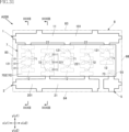
- FIG. 1 is a plan view showing a semiconductor device according to a first embodiment of the present disclosure.
- FIG. 2 is a partial plan view showing the semiconductor device according to the first embodiment of the present disclosure.
- FIG. 3 is a bottom view showing the semiconductor device according to the first embodiment of the present disclosure.
- FIG. 4 is a front view showing the semiconductor device according to the first embodiment of the present disclosure.
- FIG. 5 is a rear view showing the semiconductor device according to the first embodiment of the present disclosure.
- FIG. 6 is a left side view showing the semiconductor device according to the first embodiment of the present disclosure.
- FIG. 7 is a right side view showing the semiconductor device according to the first embodiment of the present disclosure.
- FIG. 8 is a cross-sectional view taken along line VIII-VIII in FIG. FIG.
- FIG. 9 is a cross-sectional view taken along line IX-IX in FIG.
- FIG. 10 is a cross-sectional view taken along line XX in FIG.
- FIG. 11 is a cross-sectional view taken along line XI-XI of FIG.
- FIG. 12 is a partial enlarged plan view showing the semiconductor device according to the first embodiment of the present disclosure.
- FIG. 13 is a partial enlarged plan view showing the semiconductor device according to the first embodiment of the present disclosure.
- FIG. 14 is a partial enlarged plan view showing a first modified example of the semiconductor device according to the first embodiment of the present disclosure.
- FIG. 15 is a partial enlarged plan view showing a second modified example of the semiconductor device according to the first embodiment of the present disclosure.
- FIG. 16 is a partial enlarged plan view showing a third modified example of the semiconductor device according to the first embodiment of the present disclosure.
- FIG. 17 is a partial enlarged plan view showing a fourth modified example of the semiconductor device according to the first embodiment of the present disclosure.
- FIG. 18 is a partial enlarged plan view showing a fifth modified example of the semiconductor device according to the first embodiment of the present disclosure.
- FIG. 19 is a partial enlarged plan view showing a sixth modified example of the semiconductor device according to the first embodiment of the present disclosure.
- FIG. 20 is a partial enlarged plan view showing a seventh modification of the semiconductor device according to the first embodiment of the present disclosure.
- FIG. 21 is a partial enlarged plan view showing an eighth modification of the semiconductor device according to the first embodiment of the present disclosure.
- FIG. 22 is a partial enlarged plan view showing a ninth modification of the semiconductor device according to the first embodiment of the present disclosure.
- FIG. 23 is a partially enlarged cross-sectional view taken along line AA in FIG.
- FIG. 24 is a partial enlarged plan view showing a tenth modification of the semiconductor device according to the first embodiment of the present disclosure.
- FIG. 25 is a partially enlarged cross-sectional view taken along line BB in FIG.
- FIG. 26 is a partial enlarged plan view showing an eleventh modification of the semiconductor device according to the first embodiment of the present disclosure.
- 27 is a partially enlarged cross-sectional view taken along line CC of FIG.
- FIG. 28 is a partial enlarged plan view showing a twelfth modification of the semiconductor device according to the first embodiment of the present disclosure.
- FIG. 23 is a partially enlarged cross-sectional view taken along line AA in FIG.
- FIG. 24 is a partial enlarged plan view showing a tenth modification of the semiconductor device according to the first
- FIG. 29 is a partially enlarged cross-sectional view taken along line DD in FIG.
- FIG. 30 is a plan view showing a thirteenth modification of the semiconductor device according to the first embodiment.
- FIG. 31 is a plan view showing a semiconductor device according to a second embodiment of the present disclosure.
- FIG. 32 is a cross-sectional view taken along line XXXII-XXXII in FIG. 33 is a cross-sectional view taken along line XXIII-XXXIII in FIG. 31.
- FIG. 32 is a cross-sectional view taken along line XXIII-XXXIII in FIG. 31.
- an object A is formed on an object B" and “an object A is formed on an object B” include “an object A is formed directly on an object B” and “an object A is formed on an object B with another object interposed between the object A and the object B” unless otherwise specified.
- an object A is disposed on an object B” and “an object A is disposed on an object B” include “an object A is disposed directly on an object B” and “an object A is disposed on an object B with another object interposed between the object A and the object B" unless otherwise specified.
- an object A is located on an object B includes “an object A is located on an object B in contact with an object B” and “an object A is located on an object B with another object interposed between the object A and the object B” unless otherwise specified.
- an object A overlaps an object B when viewed in a certain direction includes “an object A overlaps the entire object B” and “an object A overlaps a part of an object B.”
- a surface A faces in direction B is not limited to the case where the angle of surface A with respect to direction B is 90°, but also includes the case where surface A is tilted with respect to direction B.
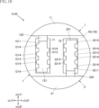
- First embodiment: 1 to 13 show a semiconductor device according to a first embodiment of the present disclosure.
- the semiconductor device A100 of this embodiment includes a plurality of leads 1 to 6, a semiconductor element 7, a wire 99, and a sealing resin 8.
- the semiconductor device A100 is mounted on a substrate, for example, to perform current switching, but the specific use of the semiconductor device A100 is not limited in any way.
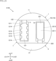
- the sealing resin 8 is omitted from FIGS. 12 and 13.
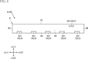
- the up-down direction in FIG. 4 will be referred to as the "thickness direction z.”
- One direction orthogonal to the thickness direction z will be referred to as the "x direction” (see, for example, FIG. 1), and the direction orthogonal to the thickness direction z and the x direction will be referred to as the "y direction.”
- the y direction and x direction may be referred to as the "first direction” and "second direction,” respectively, although this disclosure is not limited thereto.
- the multiple leads 1 to 6 appropriately fulfill the functions of supporting the semiconductor element 7, forming a conductive path that is electrically connected to the semiconductor element 7, and the like.
- the multiple leads 1 to 6 are made of metal such as copper (Cu), nickel (Ni), iron (Fe), etc.
- the multiple leads 1 to 6 are formed, for example, by subjecting a metal plate material to a process selected from punching, bending, etching, etc.
- a plating layer made of silver (Ag), Ni, gold (Au), etc. may be provided at appropriate positions on each of the multiple leads 1 to 6 as necessary.
- the multiple leads 1 to 6 are described as the first lead 1, the second lead 2, the third lead 3, the fourth lead 4, the fifth lead 5, and the island lead 6. That is, the multiple leads 1 to 6 include the first lead 1, the second lead 2, the third lead 3, the fourth lead 4, the fifth lead 5, and the island lead 6. As described below, in this embodiment, the fourth lead 4 and the island lead 6 are connected to each other. Depending on the conduction form of each lead 1 to 6, they may be configured as separate pieces, or some of the leads may be connected to each other.
- first lead 1 and the second lead 2 are formed by punching and bending a metal plate material
- the third lead 3, the fourth lead 4, the fifth lead 5, and the island lead 6 are formed by etching a metal plate material.
- the island lead 6 has a main surface 601, a back surface 602, a thick portion 61, a thin portion 62, and a plurality of extending portions 63.
- the main surface 601 is a surface facing the z1 side in the z direction, and in the illustrated example, is a smooth surface perpendicular to the z direction.
- the island lead 6 may have, for example, a recess or a groove recessed from the main surface 601 as appropriate.
- the back surface 602 is a surface facing the z2 side in the z direction, and is facing the opposite side to the main surface 601. In the illustrated example, the back surface 602 is a smooth surface perpendicular to the z direction.
- a plating layer made of Ni, titanium (Ti), or the like may be provided on the back surface 602 as appropriate.
- the thick portion 61 is a portion where the main surface 601 and the back surface 602 overlap when viewed in the z direction, and in the illustrated example, is a rectangular portion when viewed in the z direction.
- the shape of the thick portion 61 is not limited in any way.
- the thickness of the thick portion 61 in the z direction is the distance between the main surface 601 and the back surface 602.
- the thin portion 62 is a portion that overlaps with the main surface 601 when viewed in the z direction, but does not overlap with the back surface 602, and in the illustrated example, is connected so as to extend from the thick portion 61 to both sides in the x direction and both sides in the y direction when viewed in the z direction.
- the thickness of the thin portion 62 in the z direction is smaller than the distance between the main surface 601 and the back surface 602.
- the thickness of the thick portion 61 and the thickness of the thin portion 62 are not limited in any way.
- the thickness of the thick portion 61 is about 0.2 mm to 0.5 mm
- the thickness of the thin portion 62 is 0.1 mm to 0.4 mm.
- the portion of the thin-walled portion 62 that extends from the thick-walled portion 61 toward the y1 side in the y direction is larger than the portion that extends toward the y2 side.
- the multiple extensions 63 are portions that extend from the ends of the thin-walled portion 62. In the illustrated example, the multiple extensions 63 extend from the thin-walled portion 62 on both sides in the x direction. There is no limitation on the number of extensions 63, and there may be multiple extensions or one extension. In the illustrated example, two extensions 63 are provided on the x1 side in the x direction, and two extensions 63 are provided on the x2 side.
- the extensions 63 have end faces 631.
- the end faces 631 are faces that face the opposite side to the thin-walled portion 62 in the x direction, in other words, faces outward in the x direction.
- the illustrated end faces 631 are faces that are perpendicular to the x direction.
- the positions in the x direction of the two end faces 631 located on the x1 side of the x direction are the same.
- the positions in the x direction of the two end faces 631 located on the x2 side of the x direction are the same.
- the first lead 1 of this embodiment has a first main portion 11, a plurality of first branch portions 12, a first extending portion 13, a third extending portion 14, and a first standing portion 15.
- the first main portion 11 is a plate-like portion along the xy plane, and in the illustrated example, is rectangular (or approximately rectangular) with the x direction as the longitudinal direction.
- the first main portion 11 in the illustrated example has a through hole 111.
- the through hole 111 penetrates the first main portion 11 in the z direction.
- the number of through holes 111 is not limited, and may be one or more.
- the first main portion 11 has two through holes 111.
- the shape of the through holes 111 is not limited in any way, and may be a circle, an ellipse, a rectangle, a polygon, or the like, as appropriate.
- the through hole 111 is an ellipse with the x direction as the longitudinal direction when viewed in the z direction.
- the multiple first branch portions 12 extend from the first main portion 11 to the y2 side in the y direction. There is no limitation on the number of first branch portions 12, and in the illustrated example, three first branch portions 12 are provided. The multiple first branch portions 12 are arranged side by side in the x direction. The first branch portion 12 has a first connection portion 121 and a first root portion 122.
- the first connection portion 121 is a portion located on the y2 side of the first main portion 11 in the y direction.
- the first connection portion 121 is located on the z2 side of the first main portion 11 in the z direction.
- the shape of the first connection portion 121 is not limited in any way, and in the illustrated example, it has a shape whose longitudinal direction is the y direction when viewed in the z direction.
- the first connection portion 121 is perpendicular to the z direction.
- the first root portion 122 is located between the first connection portion 121 and the first main portion 11, and is connected to the first connection portion 121 and the first main portion 11.
- the first root portion 122 is inclined so that it approaches the semiconductor element 7 in the z direction (is located on the z2 side) as it moves from the first main portion 11 toward the first connection portion 121 in the y direction (as it moves from the y1 side toward the y2 side).
- the three first branches 12 include first branches 12 that have different lengths in the y direction.
- the first branch 12 located closest to the x2 side in the x direction has a shorter length in the y direction than the other first branches 12.
- the first branch 12 located closest to the x2 side in the x direction is positioned close to a third electrode 73 and a wire 99, which will be described later.
- the multiple first branches 12 may have the same length.
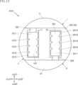
- the first connection portion 121 has a first main surface 1211, a first bonding surface 1212, and a pair of first side surfaces 1213.
- the first main surface 1211 faces the z1 side in the z direction.
- the first bonding surface 1212 faces the z2 side in the z direction and is conductively bonded to the first electrode 71.
- the pair of first side surfaces 1213 are surfaces located on both sides in the y direction.
- the first side surfaces 1213 are not limited to being flat, but include a configuration having an appropriate uneven shape.
- the first side surfaces 1213 have a plurality of first convex portions 1214. That is, the first connection portion 121 further has a plurality of first convex portions 1214. In this embodiment, the first convex portions 1214 are rectangular in shape when viewed in the z direction.
- the first extension portion 13 is a portion extending from the first main portion 11.
- the first extension portion 13 extends from the end of the first main portion 11 on the x1 side in the x direction toward the x1 side.
- the first extension portion 13 has a first end face 131.
- the first end face 131 is a surface facing the opposite side to the first main portion 11 in the x direction, in other words, a surface facing the x1 side, which is the outside in the x direction.
- the illustrated first end face 131 is a surface perpendicular to the x direction.
- the position of the first end face 131 in the x direction is the same as the position in the x direction of the multiple end faces 631 located on the x1 side of the x direction.
- the third extension portion 14 is a portion extending from the first main portion 11.
- the third extension portion 14 extends from the end of the first main portion 11 on the x2 side in the x direction toward the x2 side.
- the third extension portion 14 has a third end face 141.
- the third end face 141 is a surface facing the opposite side to the first main portion 11 in the x direction, in other words, a surface facing the x2 side, which is the outside in the x direction.
- the illustrated third end face 141 is a surface perpendicular to the x direction.
- the position of the third end face 141 in the x direction is the same as the position in the x direction of the multiple end faces 631 located on the x2 side in the x direction.
- the first standing portion 15 is connected to the end of the first main portion 11 on the y1 side in the y direction, opposite the first branch portion 12.
- the first standing portion 15 extends from the first main portion 11 to the z2 side in the z direction.
- the shape of the first standing portion 15 is not limited in any way, and in the illustrated example, it is rectangular with the x direction as the longitudinal direction. In the illustrated example, the center of the first standing portion 15 in the x direction is the same as the center of the first main portion 11 in the x direction.
- the tip of the first upright portion 15 of the first lead 1 on the z2 side in the z direction is conductively joined to the third lead 3 via a fourth conductive joint 94.
- the fourth conductive joint 94 is, for example, solder, Ag paste material, Ag sintered material, Cu sintered material, etc.
- the second lead 2 is disposed on the z1 side in the z direction relative to the third lead 3, the fourth lead 4, the fifth lead 5, and the island lead 6.
- the second lead 2 is disposed on the y2 side in the y direction relative to the first lead 1.
- the second lead 2 of this embodiment has a second main portion 21, a plurality of second branch portions 22, a second extending portion 23, a fourth extending portion 24, a second standing portion 25, and a connecting portion 29.
- the second main portion 21 is a plate-like portion along the xy plane, and in the illustrated example, is rectangular (or approximately rectangular) with the x direction as the longitudinal direction.
- the first main portion 11 and the second main portion 21 are disposed on opposite sides of each other in the y direction with respect to the semiconductor element 7.
- the second main portion 21 in the illustrated example has a through hole 211.
- the through hole 211 penetrates the second main portion 21 in the z direction.
- the number of through holes 211 is not limited, and may be one or more.
- the second main portion 21 has two through holes 211.
- the shape of the through hole 211 is not limited in any way, and may be a circle, an ellipse, a rectangle, a polygon, or the like, as appropriate.
- the through hole 211 is an ellipse with the x direction as the longitudinal direction when viewed in the z direction.
- the second main portion 21 is disposed at the same position as the first main portion 11 in the z direction.
- the multiple second branch portions 22 extend from the second main portion 21 toward the y1 side in the y direction. There is no limitation on the number of second branch portions 22, and in the illustrated example, two second branch portions 22 are provided. The multiple second branch portions 22 are arranged side by side in the x direction. The second branch portion 22 has a second connection portion 221 and a second root portion 222.
- the second connection portion 221 is a portion located on the y1 side of the second main portion 21 in the y direction.
- the second connection portion 221 is located on the z2 side of the second main portion 21 in the z direction.
- the shape of the second connection portion 221 is not limited in any way, and in the illustrated example, it has a shape whose longitudinal direction is the y direction when viewed in the z direction.
- the second connection portion 221 is perpendicular to the z direction.
- the second root portion 222 is located between the second connection portion 221 and the second main portion 21, and is connected to the second connection portion 221 and the second main portion 21.
- the second root portion 222 is inclined so that it approaches the semiconductor element 7 in the z direction (is located on the z2 side) as it moves from the second main portion 21 toward the second connection portion 221 in the y direction (as it moves from the y2 side toward the y1 side).
- the two second branches 22 have the same length in the y direction.
- the multiple second branches 22 may have different lengths in the y direction.
- the second connection portion 221 has a second main surface 2211, a second bonding surface 2212, and a pair of second side surfaces 2213.
- the second main surface 2211 faces the z1 side in the z direction.
- the second bonding surface 2212 faces the z2 side in the z direction and is conductively bonded to the second electrode 72.
- the pair of second side surfaces 2213 are surfaces located on both sides in the y direction.
- the second side surface 2213 is not limited to a flat surface, and may have an uneven shape as appropriate.
- the second side surface 2213 has a plurality of second convex portions 2214. That is, the second connection portion 221 further has a plurality of second convex portions 2214.
- the second convex portion 2224 has a rectangular shape when viewed in the z direction.
- the first convex portion 1214 on the x1 side and the first convex portion 1214 on the x2 side overlap when viewed in the x direction.
- the second convex portion 2214 on the x1 side and the second convex portion 2214 on the x2 side overlap when viewed in the x direction.
- the first convex portion 1214 and the second convex portion 2214 do not overlap when viewed in the x direction.
- the center of the first convex portion 1214 in the y direction and the center of the second convex portion 2214 in the y direction are offset from each other.
- the first convex portion 1214 and the second convex portion 2214 may overlap when viewed in the x direction.
- the first side surface 1213 can also be said to have a plurality of first concave portions 1215.
- the first connection portion 121 can also be said to have a plurality of first concave portions 1215.
- the first concave portion 1215 has a rectangular shape when viewed in the z direction.
- the second side surface 2213 can also be said to have a plurality of second concave portions 2215.
- the second connection portion 221 can also be said to have a plurality of second concave portions 2215.
- the second concave portion 2215 has a rectangular shape when viewed in the z direction.
- the second extension portion 23 is a portion extending from the second main portion 21.
- the second extension portion 23 extends from the end of the second main portion 21 on the x1 side in the x direction toward the x1 side.
- the second extension portion 23 has a second end face 231.
- the second end face 231 is a surface facing the opposite side to the second main portion 21 in the x direction, in other words, a surface facing the x1 side, which is the outer side in the x direction.
- the illustrated second end face 231 is a surface perpendicular to the x direction.
- the position of the second end face 231 in the x direction is the same as that of the first end face 131 and the end face 631 located on the x1 side in the x direction.
- the fourth extension portion 24 is connected to the second main portion 21 via a connecting portion 29.
- the connecting portion 29 has a smaller dimension in the y direction than the second main portion 21 and the fourth extension portion 24.
- the fourth extension portion 24 is not limited to a configuration in which it is directly connected to the second main portion 21, but includes a configuration in which it is connected to the second main portion 21 via other portions.
- the above-mentioned first extension portion 13 and third extension portion 14 are also not limited to a configuration in which they are directly connected to the first main portion 11, but include a configuration in which they are connected to the first main portion 11 via other portions.
- the fourth extension portion 24 extends along the y direction.
- the fourth extension portion 24 has a fourth end surface 241.
- the fourth end surface 241 is a surface that faces the opposite side to the second main portion 21 in the y direction, in other words, a surface that faces the y2 side, which is the outside in the y direction.
- the illustrated fourth end surface 241 is a surface perpendicular to the y direction.
- the second standing portion 25 is connected to the end of the second main portion 21 on the y2 side in the y direction, opposite the second branch portion 22.
- the second standing portion 25 extends from the second main portion 21 to the z2 side in the z direction.
- the shape of the second standing portion 25 is not limited in any way, and in the illustrated example, it is rectangular with the x direction as the longitudinal direction. In the illustrated example, the center of the second standing portion 25 in the x direction is the same as the center of the second main portion 21 in the x direction.
- the tip of the second upright portion 25 of the second lead 2 on the z2 side in the z direction is conductively joined to the fourth lead 4 via a fifth conductive joint 95.
- the fifth conductive joint 95 is, for example, solder.
- the third lead 3 is disposed at a distance from the island lead 6 on the y1 side in the y direction.
- the center of the third lead 3 in the x direction is at approximately the same position in the x direction as the center of the island lead 6 in the x direction.
- the third lead 3 has a main surface 301, a back surface 302, a thick portion 31, a thin portion 32, and a plurality of extending portions 33.
- the main surface 301 is a surface facing the z1 side in the z direction, and in the illustrated example, is a smooth surface perpendicular to the z direction.
- the third lead 3 may have, for example, a recess or groove recessed from the main surface 301 as appropriate.
- the first upright portion 15 described above is joined to the main surface 301 via the fourth conductive joint 94.
- the back surface 302 is a surface facing the z2 side in the z direction, and faces the opposite side to the main surface 301. In the illustrated example, the back surface 302 is a smooth surface perpendicular to the z direction.
- a plating layer made of Ni, Ti, or the like may be provided on the back surface 302 as appropriate.
- the main surface 301 is located at approximately the same position as the main surface 601 in the z direction
- the back surface 302 is located at approximately the same position as the back surface 602.
- the thick portion 31 is a portion where the main surface 301 and the back surface 302 overlap when viewed in the z direction.
- the thick portion 31 is a rectangular portion with the x direction as the longitudinal direction when viewed in the z direction.
- the shape of the thick portion 31 is not limited in any way.
- the thickness of the thick portion 31 in the z direction is the distance between the main surface 301 and the back surface 302.
- the thin portion 32 is a portion that overlaps the main surface 301 when viewed in the z direction and does not overlap the back surface 302.
- the thin portion 32 is connected to the thick portion 31 so as to extend to both sides in the x direction and to the y2 side in the y direction when viewed in the z direction.
- the thin portion 32 has a portion that is connected to the thick portion 31 so as to extend to the y1 side in the y direction when viewed in the z direction, and this portion is sandwiched between the extension portions 33 in the x direction.
- the thickness of the thin portion 32 in the z direction is smaller than the distance between the main surface 301 and the back surface 302.
- the thickness of the thick portion 31 and the thin portion 32 are no limitations. In this embodiment, the thickness of the thick portion 31 is approximately the same as the thickness of the thick portion 61, and the thickness of the thin portion 32 is approximately the same as the thickness of the thin portion 62.
- the multiple extension portions 33 are portions that extend from the end of the thick portion 31. In the illustrated example, the multiple extension portions 33 extend from the thick portion 31 to the y1 side in the y direction. There is no limitation on the number of extension portions 33, and there may be multiple extension portions 33 or there may be only one extension portion. In the illustrated example, four extension portions 33 are provided.
- the extension portion 33 has an end face 331.
- the end face 331 is a surface that faces the opposite side to the thick portion 31 in the y direction, in other words, a surface that faces the y1 side, which is the outside in the y direction.
- the illustrated end face 331 is a surface that is perpendicular to the y direction.
- the multiple end faces 331 are located at the same position in the y direction.
- the fourth lead 4 is disposed on the y2 side in the y direction with respect to the island lead 6.
- the center of the fourth lead 4 in the x direction is located on the x1 side in the x direction with respect to the center of the island lead 6 in the x direction.
- the fourth lead 4 and the island lead 6 are connected by a relay portion 49.
- the fourth lead 4 may be separated from the island lead 6.
- the fourth lead 4 has a main surface 401, a back surface 402, a thick portion 41, a thin portion 42, and a plurality of extending portions 43.
- the main surface 401 is a surface facing the z1 side in the z direction, and in the illustrated example, is a smooth surface perpendicular to the z direction.
- the fourth lead 4 may have, for example, a recess or groove recessed from the main surface 401 as appropriate.
- the second upright portion 25 described above is joined to the main surface 401 via the fifth conductive joint 95.
- the back surface 402 is a surface facing the z2 side in the z direction, and faces the opposite side to the main surface 401. In the illustrated example, the back surface 402 is a smooth surface perpendicular to the z direction.
- a plating layer made of Ni, Ti, or the like may be provided on the back surface 402 as appropriate.
- the main surface 401 is located at approximately the same position as the main surface 601 in the z direction
- the back surface 402 is located at approximately the same position as the back surface 602.
- the thick portion 41 is a portion where the main surface 401 and the back surface 402 overlap when viewed in the z direction.
- the thick portion 41 is a rectangular portion with the x direction as the longitudinal direction when viewed in the z direction.
- the shape of the thick portion 41 is not limited in any way.
- the thickness of the thick portion 41 in the z direction is the distance between the main surface 401 and the back surface 402. In this embodiment, the dimension of the thick portion 41 in the x direction is smaller than the dimension of the thick portion 31 in the x direction.
- the thin portion 42 is a portion that overlaps with the main surface 401 when viewed in the z direction and does not overlap with the back surface 402.
- the thin portion 42 is connected to the thick portion 41 so as to extend to both sides in the x direction and to the y1 side in the y direction when viewed in the z direction.
- the thin portion 42 has a portion that is connected to the thick portion 41 so as to extend to the y2 side in the y direction when viewed in the z direction, and this portion is sandwiched between the extension portions 43 in the x direction.
- the thickness of the thin portion 42 in the z direction is smaller than the distance between the main surface 401 and the back surface 402.
- the thicknesses of the thick portion 41 and the thin portion 42 are not limited in any way. In this embodiment, the thickness of the thick portion 41 is approximately the same as the thickness of the thick portion 61, and the thickness of the thin portion 42 is approximately the same as the thickness of the thin portion 62.
- the multiple extension portions 43 are portions extending from the end of the thick portion 41.
- the multiple extension portions 43 extend from the thick portion 41 to the y2 side in the y direction.
- three extension portions 43 are provided. The positions in the x direction of these three extension portions 43 are approximately the same as the positions in the x direction of the three extension portions 33 located on the x1 side in the x direction among the multiple extension portions 33.
- the extension portion 43 has an end face 431.
- the end face 431 is a surface facing the opposite side to the thick portion 41 in the y direction, in other words, a surface facing the y2 side, which is the outside in the y direction.
- the illustrated end face 431 is a surface perpendicular to the y direction.
- the positions in the y direction of the multiple end faces 431 are the same as each other.
- the positions of the multiple end faces 431 in the y direction are the same as those of the fourth end face 241.
- the fifth lead 5 is disposed on the y2 side in the y direction with respect to the island lead 6.
- the center in the x direction of the fifth lead 5 is located on the x2 side in the x direction with respect to the center in the x direction of the island lead 6.
- the fifth lead 5 is disposed on the x2 side in the x direction with respect to the fourth lead 4.
- the fifth lead 5 has a main surface 501, a back surface 502, a thick portion 51, a thin portion 52, and an extending portion 53.
- the main surface 501 is a surface facing the z1 side in the z direction, and in the illustrated example, is a smooth surface perpendicular to the z direction.
- the fifth lead 5 may have, for example, a recess or groove recessed from the main surface 501 as appropriate.
- a wire 99 is bonded to the main surface 501.
- the back surface 502 is a surface facing the z2 side in the z direction, and faces the opposite side to the main surface 501. In the illustrated example, the back surface 502 is a smooth surface perpendicular to the z direction.
- a plating layer made of Ni, Ti, or the like may be provided on the back surface 502 as appropriate.
- the main surface 501 is located at approximately the same position as the main surface 601 in the z direction
- the back surface 502 is located at approximately the same position as the back surface 602.
- the thick portion 51 is a portion where the main surface 501 and the back surface 502 overlap when viewed in the z direction.
- the thick portion 51 is a rectangular portion when viewed in the z direction.
- the shape of the thick portion 51 is not limited in any way.
- the thickness of the thick portion 51 in the z direction is the distance between the main surface 501 and the back surface 502.
- the dimension of the thick portion 51 in the x direction is smaller than the dimension of the thick portion 31 and the thick portion 41 in the x direction.
- the thin portion 32 is a portion that overlaps with the main surface 301 when viewed in the z direction and does not overlap with the back surface 302.
- the thin portion 32 is connected so as to extend from the thick portion 51 to both sides in the x direction and to the y1 side in the y direction when viewed in the z direction.
- the thickness of the thin portion 52 in the z direction is smaller than the distance between the main surface 501 and the back surface 502.
- the thickness of the thick portion 51 and the thickness of the thin portion 52 are not limited in any way. In this embodiment, the thickness of thick portion 51 is approximately the same as the thickness of thick portion 61, and the thickness of thin portion 52 is approximately the same as the thickness of thin portion 62.
- the extension portion 53 is a portion extending from the end of the thick portion 51. In the illustrated example, the extension portion 53 extends from the thick portion 51 to the y2 side in the y direction. There is no limitation on the number of extension portions 53, and there may be multiple extension portions 53 or there may be only one extension portion. In the illustrated example, one extension portion 53 is provided. The position of the extension portion 53 in the x direction is approximately the same as the position in the x direction of the extension portion 33 located furthest on the x2 side in the x direction among the multiple extension portions 33. The extension portion 53 has an end face 531.
- the end face 531 is a face facing the opposite side to the thick portion 51 in the y direction, in other words, a face facing the y2 side, which is the outside in the y direction.
- the illustrated end face 531 is a face perpendicular to the y direction.
- the position of the end face 531 in the y direction is the same as the fourth end face 241 and the multiple end faces 431.
- the semiconductor element 7 is an element that exerts the electrical function of the semiconductor device A100.
- the specific configuration of the semiconductor element 7 is not limited in any way, and in this embodiment, the semiconductor element 7 is a transistor using a nitride semiconductor, more specifically, a GaN-HEMT (High Electron Mobility Transistor) element using gallium nitride (GaN).
- the semiconductor element 7 is not limited to one using a nitride semiconductor, and other semiconductors such as silicon (Si) and silicon carbide (SiC) may be used.
- the semiconductor element 7 is not limited to a HEMT, and may be other transistors such as a MOSFET (Metal-Oxide-Semiconductor Field Effect Transistor) and an IGBT (Insulated Gate Bipolar Transistor).
- MOSFET Metal-Oxide-Semiconductor Field Effect Transistor
- IGBT Insulated Gate Bipolar Transistor
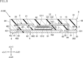
- the semiconductor element 7 is mounted on the thick portion 61 of the island lead 6. As shown in FIGS. 1, 2, and 8 to 12, the semiconductor element 7 has an element body 70, a plurality of first electrodes 71, a plurality of second electrodes 72, and a third electrode 73.
- the element body 70 is, for example, a portion in which a substrate layer, a buffer layer, and a nitride layer (all not shown) are laminated.
- the element body 70 has an element main surface 701 and an element back surface 702.
- the element main surface 701 is a surface facing the z1 side in the z direction.
- the element back surface 702 is a surface facing the z2 side in the z direction, and faces the opposite side to the element main surface 701.
- a metal layer is provided on the element back surface 702. As shown in Figures 12 to 14, this metal layer and the main surface 601 of the island lead 6 are joined by a first conductive joint 91.
- the first conductive joint 91 is, for example, solder, Ag paste material, Ag sintered material, Cu sintered material, etc.
- the above-mentioned metal layer is provided for joining by the first conductive joint 91, but the configuration may not include the metal layer. Alternatively, the metal layer may be configured to have the same potential as, for example, the second electrode 72, etc.
- the semiconductor element 7 is positioned so that it overlaps with a portion of the thick portion 61 and a portion of the thin portion 62 of the island lead 6 when viewed in the z direction.
- the first electrodes 71, the second electrodes 72, and the third electrodes 73 are arranged on the element main surface 701.
- the number of the first electrodes 71 and the second electrodes 72 is not limited in any way. In the illustrated example, three first electrodes 71 and two second electrodes 72 are provided.
- the number of the first electrodes 71 is the same as the number of the first branches 12, and the number of the second electrodes 72 is the same as the number of the second branches 22.
- the first electrode 71 is an electrode that functions as a drain electrode.
- the second electrode 72 is an electrode that functions as a source electrode.
- the first electrodes 71 and the second electrodes 72 are arranged alternately in the x direction.
- the shapes of the first electrodes 71 and the second electrodes 72 are not limited in any way, and in the illustrated example, they are shaped such that the y direction is the longitudinal direction, and more specifically, they are tapered.
- the first connection parts 121 of the first branch parts 12 of the first lead 1 are individually conductively joined to the first electrodes 71 via second conductive joint parts 92.
- the second conductive joint parts 92 are, for example, solder, Ag paste material, Ag sintered material, Cu sintered material, etc.
- the second connection parts 221 of the second branch parts 22 of the second lead 2 are individually conductively joined to the second electrodes 72 via third conductive joint parts 93.
- the third conductive joint parts 93 are, for example, solder, Ag paste material, Ag sintered material, Cu sintered material, etc.
- the third electrode 73 is an electrode that functions as a gate electrode.
- the number of the third electrodes 73 is not limited, and may be one or more. In the illustrated example, one third electrode 73 is provided.
- the third electrode 73 is disposed, for example, at one of the four corners of the element main surface 701. In the illustrated example, the third electrode 73 is disposed near the corner of the element main surface 701 on the x2 side in the x direction and the y2 side in the y direction.
- the third electrode 73 is disposed on the y2 side in the y direction with respect to the first electrode 71 on the x2 side in the x direction of the two first electrodes 71.
- a wire 99 is joined to the third electrode 73, and the third electrode 73 is electrically connected to the fifth lead 5 via the wire 99.
- a conductive member made of a metal plate material may be used to electrically connect the third electrode 73 and the fifth lead 5.
- the sealing resin 8 covers a portion of each of the leads 1 to 6, the semiconductor element 7, and the wires 99, and is made of an insulating material such as an epoxy resin. As shown in Figures 1 to 11, the sealing resin 8 has a first surface 81, a second surface 82, a third surface 83, a fourth surface 84, a fifth surface 85, and a sixth surface 86, and is in the shape of a rectangular parallelepiped.
- the first surface 81 is a surface facing the z1 side in the z direction. In the illustrated example, the first surface 81 is a plane perpendicular to the z direction.
- the second surface 82 is a surface facing the z2 side in the z direction. In the illustrated example, the second surface 82 is a plane perpendicular to the z direction.
- the third surface 83 is a surface facing the y1 side in the y direction. In the illustrated example, the third surface 83 is a plane perpendicular to the y direction.
- the fourth surface 84 is a surface facing the y2 side in the y direction. In the illustrated example, the fourth surface 84 is a plane perpendicular to the y direction.
- the fifth surface 85 is a surface facing the x1 side in the x direction. In the illustrated example, the fifth surface 85 is a plane perpendicular to the x direction.
- the sixth surface 86 is a surface facing the x2 side in the x direction. In the illustrated example, the sixth surface 86 is a plane perpendicular to the x direction.
- the back surface 602 of the island lead 6, the back surface 302 of the third lead 3, the back surface 402 of the fourth lead 4, and the back surface 502 of the fifth lead 5 are exposed on the z2 side in the z direction.
- the second surface 82, the back surface 602 of the island lead 6, the back surface 302 of the third lead 3, the back surface 402 of the fourth lead 4, and the back surface 502 of the fifth lead 5 are flush with one another.
- all or any of the back surface 602 of the island lead 6, the back surface 302 of the third lead 3, the back surface 402 of the fourth lead 4, and the back surface 502 of the fifth lead 5 may protrude slightly from the second surface 82.
- the third surface 83 From the third surface 83, multiple end faces 331 of the third lead 3 are exposed on the y1 side in the y direction.
- the third surface 83 and the multiple end faces 331 of the third lead 3 are flush with each other. However, all or any of the multiple end faces 331 may protrude slightly from the third surface 83.
- the fourth end face 241 of the second lead 2, the multiple end faces 431 of the fourth lead 4, and the end face 531 of the fifth lead 5 are exposed on the y2 side in the y direction.
- the fourth surface 84, the fourth end face 241 of the second lead 2, the multiple end faces 431 of the fourth lead 4, and the end face 531 of the fifth lead 5 are flush with one another.
- all or any of the fourth end face 241 of the second lead 2, the multiple end faces 431 of the fourth lead 4, and the end face 531 of the fifth lead 5 may protrude slightly from the fourth surface 84.
- the first end surface 131 of the first lead 1, the second end surface 231 of the second lead 2, and the multiple end surfaces 631 of the island lead 6 are exposed on the x1 side in the x direction.
- the fifth surface 85, the first end surface 131 of the first lead 1, the second end surface 231 of the second lead 2, and the multiple end surfaces 631 of the island lead 6 are flush with one another. However, all or any of the first end surface 131 of the first lead 1, the second end surface 231 of the second lead 2, and the multiple end surfaces 631 of the island lead 6 may protrude slightly from the fifth surface 85.
- the third end surface 141 of the first lead 1 and the multiple end surfaces 631 of the island lead 6 are exposed on the x2 side in the x direction.
- the sixth surface 86, the third end surface 141 of the first lead 1, and the multiple end surfaces 631 of the island lead 6 are flush with one another. However, all or any of the third end surface 141 of the first lead 1 and the multiple end surfaces 631 of the island lead 6 may protrude slightly from the sixth surface 86.
- the semiconductor device A100 is mounted on a circuit board (not shown) or the like, with the back surfaces 302, 402, and 502 exposed from the second surface 82 of the sealing resin 8 serving as mounting terminals. That is, the mounting surface of the semiconductor device A100 is the z2 side, which is opposite to the z1 side, which is the side to which the element principal surface 701 of the semiconductor element 7 faces in the z direction.
- the back surface 602 is used as a heat dissipation surface for dissipating heat from the semiconductor element 7.
- the first connection portion 121 has a first convex portion 1214 or a first concave portion 1215
- the second connection portion 221 has a second convex portion 2214 or a second concave portion 2215. This increases the contact area between the sealing resin 8 and the first connection portion 121 and the second connection portion 221, making it possible to suppress peeling of the sealing resin 8.
- the first convex portion 1214 and the second convex portion 2214 are configured so as not to overlap when viewed in the x-direction. This makes it possible to increase the distance between the first convex portion 1214 and the second convex portion 2214, which are positioned opposite each other, and makes it possible to prevent unintended short circuits, etc. from occurring.
- FIGS. 13 to 20 show modified examples and other embodiments of the present disclosure.
- elements that are the same as or similar to those in the above-described embodiment are given the same reference numerals as in the above-described embodiment.
- the configurations of the various parts in each modified example and each embodiment can be combined with each other as appropriate to the extent that no technical contradictions arise.
- First Modification of First Embodiment 14 shows a first modified example of the semiconductor device A100.
- the shapes of the first recess 1215 and the second recess 2215 are different from those of the semiconductor device A100.
- first recess 1215 and the second recess 2215 are triangular when viewed in the z direction.
- the multiple first recesses 1215 are adjacent to each other and spaced apart.
- the multiple second recesses 2215 are adjacent to each other and spaced apart.
- This modified example also increases the contact area between the sealing resin 8 and the first connection portion 121 and the second connection portion 221, making it possible to suppress peeling of the sealing resin.
- the size of the cross section perpendicular to the x-direction of the first recess 1215 and the second recess 2215 is not limited to a constant size, and may be configured to become smaller from the outside to the inside in the x-direction.
- Second Modification of First Embodiment 15 shows a second modified example of the semiconductor device A 100.
- the shapes of the first recess 1215 and the second recess 2215 are different from those in the above-described example.
- the first recess 1215 and the second recess 2215 are trapezoidal when viewed in the z direction, and the size of the cross section perpendicular to the x direction becomes smaller going from the outside to the inside in the x direction.
- the multiple first recesses 1215 are adjacent to each other and spaced apart.
- the multiple second recesses 2215 are adjacent to each other and spaced apart. Unlike FIG. 15, there may be only one first recess 1215 or only one second recess 2215. Furthermore, there may be a configuration having only either the first recess 1215 or the second recess 2215.
- This modified example also increases the contact area between the sealing resin 8 and the first connection portion 121 and the second connection portion 221, making it possible to prevent the sealing resin from peeling off.
- Second Modification of First Embodiment 16 shows a third modified example of the semiconductor device A 100.
- the shapes of the first recess 1215 and the second recess 2215 are different from those in the above-described example.
- the first recess 1215 has five sides and is shaped to narrow toward the inside of the first connection portion 121 in the x-direction.
- the second recess 2215 has five sides and is shaped to narrow toward the inside of the second connection portion 221 in the x-direction.
- This modified example also increases the contact area between the sealing resin 8 and the first connection portion 121 and the second connection portion 221, making it possible to prevent the sealing resin 8 from peeling off.
- FIG. 17 shows a fourth modification of the semiconductor device A 100.
- the shapes of the first recess 1215 and the second recess 2215 are different from those in the above-described example.
- the first recess 1215 has a trapezoidal shape when viewed in the z direction, and the size of the cross section perpendicular to the x direction increases from the outside to the inside in the x direction.
- the second recess 2215 has a trapezoidal shape when viewed in the z direction, and the size of the cross section perpendicular to the x direction increases from the outside to the inside in the x direction.
- the contact area between the sealing resin 8 and the first connecting portion 121 and the second connecting portion 221 is increased, and peeling of the sealing resin 8 can be suppressed.
- the size of the cross section perpendicular to the x direction of the first recess 1215 and the second recess 2215 is not limited to a constant size, and may be configured to increase from the outside to the inside in the x direction.
- the shape of the first recess 1215 and the second recess 2215 in a plan view (shape as viewed in the z direction) is not limited in any way, and the number of them is also arbitrary.
- the shapes of the first convex portion 1214, the first recess 1215, the second convex portion 2214, and the second recess 2215 are not limited to the shapes shown in the figures, and the number of them is also arbitrary.
- Fifth Modification of First Embodiment 18 shows a fifth modified example of the semiconductor device A 100.
- the arrangement of the first convex portion 1214 and the second convex portion 2214 is different from that of the above-described example.
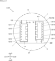
- the first convex portion 1214 on the x1 side and the first convex portion 1214 on the x2 side do not overlap each other when viewed in the x direction.
- the second convex portion 2214 on the x1 side and the second convex portion on the x2 side do not overlap each other when viewed in the x direction.
- the first convex portion 1214 on the x2 side and the second convex portion 2214 on the x1 side do not overlap each other when viewed in the x direction.
- the center in the y direction of the first convex portion 1214 on the x2 side and the center in the y direction of the second convex portion 2214 on the x1 side do not overlap each other when viewed in the x direction.
- the first convex portion 1214, the first concave portion 1215 (the length between adjacent first convex portions 1214), the second convex portion 2214, and the second concave portion 2215 (the length between adjacent second convex portions 2214) are all equal, but they may be unequal.
- the first convex portion 1214 on the x1 side and the first convex portion 1214 on the x2 side may each partially overlap when viewed in the x direction.
- the first convex portion 1214 on the x2 side and the second convex portion 2214 on the x1 side may each partially overlap when viewed in the x direction.
- This modified example also increases the contact area between the sealing resin 8 and the first connection portion 121 and the second connection portion 221, making it possible to suppress peeling of the sealing resin 8.
- the first convex portion 1214 on the xx1 side and the first convex portion 1214 on the x2 side do not overlap each other when viewed in the x direction
- the second convex portion 2214 on the x1 side and the second convex portion on the x2 side do not overlap each other when viewed in the x direction, so it is possible to prevent the size of the first connection portion 121 and the second connection portion 221 in the x direction from becoming too small locally, and it is possible to effectively ensure the area through which current flows.
- FIG. 19 shows a sixth modified example of the semiconductor device A 100.
- the arrangement of the first recess 1215 and the second recess 2215 is different from that of the above-described example.
- first recess 1215 and the second recess 2215 have a triangular shape when viewed in the z direction. Adjacent first recesses 1215 are connected to each other, and adjacent second recesses 2215 are also connected to each other.
- This modified example also increases the contact area between the sealing resin 8 and the first and second connection parts 121 and 221, making it possible to suppress peeling of the sealing resin 8.
- a configuration in which adjacent first recesses 1215 and adjacent second recesses 2215 are connected is advantageous for increasing the contact area between the sealing resin 8 and the first and second connection parts 121 and 221.
- FIG. 20 shows a seventh modified example of the semiconductor device A 100.
- the arrangement of the first convex portion 1214 and the second convex portion 2214 is different from that of the above-described example.
- the first side surface 1213 on the x2 side of the first connection portion 121 has the first convex portion 1214 (first concave portion 1215), and the first side surface 1213 on the x1 side does not have the first convex portion 1214 (first concave portion 1215).
- the second side surface 2213 on the x1 side of the second connection portion 221 has the second convex portion 2214 (second concave portion 2215), and the second side surface 2213 on the x2 side does not have the second convex portion 2214 (second concave portion 2215).
- the first side surface 1213 on the x1 side may have the first convex portion 1214 (first concave portion 1215), and the second side surface 2213 on the x2 side may have the second convex portion 2214 (second concave portion 2215).
- the contact surface between the sealing resin 8 and the first connection portion 121 and the second connection portion 221 is increased, making it less likely that the sealing resin 8 will peel off.
- the first connection portion 121 and the second connection portion 221 may be configured to have the first convex portion 1214 (first concave portion 1215) and the second convex portion 2214 (second concave portion 2215) only on one side in the x direction.
- FIG. 21 shows an eighth modified example of the semiconductor device A100.
- the first connection portion 121 has a first convex portion 1214 (first concave portion 1215), and the second connection portion 221 does not have a second convex portion 2214 (second concave portion 2215).
- the second connection portion 221 may have the second convex portion 2214 (second concave portion 2215), and the first connection portion 121 may not have the first convex portion 1214 (first concave portion 1215).
- This modified example also increases the contact area between the sealing resin 8 and the first connection portion 121 and the second connection portion 221, making it possible to prevent the sealing resin 8 from peeling off.
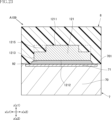
- Ninth Modification of First Embodiment 22 and 23 show a ninth modification of the semiconductor device A 100.
- the shapes of the first recess 1215 and the second recess 2215 are different from those in the above-described example.
- first recess 1215 reaches the first main surface 1211, but does not reach the first joining surface 1212.
- second recess 2215 reaches the second main surface 2211, but does not reach the second joining surface 2212.
- the shapes of the first recess 1215 and the second recess 2215 are both rectangular parallelepipeds, but the specific shape is not important.
- the number of first recesses 1215 and second recesses 2215 is arbitrary.
- the sealing resin 8 enters the first recess 1215 and the second recess 2215, increasing the contact area between the sealing resin 8 and the first connection portion 121 and the second connection portion 221, and thus preventing the sealing resin 8 from peeling off.
- Tenth Modification of First Embodiment 24 and 25 show a tenth modified example of the semiconductor device A100.
- the first convex portion 1214 reaches the first main surface 1211 and does not reach the first bonding surface 1212.
- the first convex portion 1214 protrudes from the first electrode 71 in the x direction when viewed in the z direction.
- the sealing resin 8 is filled between the first convex portion 1214 and the semiconductor element 7.
- the second convex portion 2214 reaches the second main surface 2211 and does not reach the second bonding surface 2212 when viewed in the z direction.
- the second convex portion 2214 protrudes from the second electrode 72 in the x direction when viewed in the z direction.
- the sealing resin 8 is filled between the second convex portion 2214 and the semiconductor element 7.
- the shapes of the first convex portion 1214 and the second convex portion 2214 when viewed in the z direction are triangular, but the specific shape is not important.
- the number of first convex portions 1214 and second convex portions 2214 is arbitrary.
- This modified example also increases the contact area between the sealing resin 8 and the first connection portion 121 and the second connection portion 221.
- the sealing resin 8 penetrates into the z2 side of the first convex portion 1214 and the second convex portion 2214 in the z direction, thereby further suppressing peeling of the sealing resin 8. Since the first convex portion 1214 protrudes from the first electrode 71 when viewed in the z direction, the sealing resin 8 can be more reliably filled between the first convex portion 1214 and the semiconductor element 7. Since the second convex portion 2214 protrudes from the second electrode 72 when viewed in the z direction, the sealing resin 8 can be more reliably filled between the second convex portion 2214 and the semiconductor element 7.
- 26 and 27 show an eleventh modified example of the semiconductor device A100.
- the first convex portion 1214 does not reach both the first main surface 1211 and the first bonding surface 1212.
- the second convex portion 2214 does not reach both the second main surface 2211 and the second bonding surface 2212.
- the shapes of the first convex portion 1214 and the second convex portion 2214 are both rectangular parallelepipeds, but the specific shapes are not important.
- the number of the first convex portions 1214 and the second convex portions 2214 is arbitrary.
- This modified example also increases the contact area between the sealing resin 8 and the first connection portion 121 and the second connection portion 221, making it possible to prevent the sealing resin 8 from peeling off.
- Twelfth Modification of First Embodiment 28 and 29 show a twelfth modification of the semiconductor device A 100.
- the configurations of the first recess 1215 and the second recess 2215 are different from those in the above-described example.
- the first connection portion 121 has a first recess 1215 on the first main surface 1211.
- the second connection portion 221 has a second recess 2215 on the second main surface 2211.
- the first recess 1215 does not reach the first joining surface 1212.
- the second recess 2215 does not reach the second joining surface 2212.
- the first convex portion 1214 and the second convex portion 2214 are both rectangular parallelepipeds, but the specific shape is not important.
- the number of first recesses 1215 and second recesses 2215 is arbitrary, and a configuration having only either the first recess 1215 or the second recess 2215 may be used.
- the sealing resin 8 enters the first recess 1215 and the second recess 2215, increasing the contact area between the sealing resin 8 and the first connection portion 121 and the second connection portion 221, and thus preventing the sealing resin 8 from peeling off.
- FIG. 30 shows a thirteenth modified example of the semiconductor device A 100.
- the semiconductor device A 113 of this modified example has a configuration generally common to the above-mentioned semiconductor device A 100, except for the points described below.
- the first lead 1 does not have the above-mentioned through hole 111, and the second lead 2 does not have the through hole 211.
- the number of the multiple extensions 33 of the third lead 3 and the multiple extensions 43 of the fourth lead 4 differs from that of the semiconductor device A100.
- the size in the x direction of the first main portion 11 of the first lead 1 is such that the size of the portion located on the y1 side in the y direction is smaller than the size of the portion located on the y2 side in the y direction, and is the same (or approximately the same) as the size in the x direction of the first standing portion 15.
- the size in the x direction of the second main portion 21 of the second lead 2 is such that the size of the portion located on the y2 side in the y direction is smaller than the size of the portion located on the y1 side in the y direction, and is the same (or approximately the same) as the size in the x direction of the second standing portion 25.
- the distance in the y direction between the y2 side edge of the main surface 101 in the y direction and the first extension portion 13 and the third extension portion 14 is smaller in this modified example than the distance in the semiconductor device A100.
- the distance in the y direction between the y1 side edge of the main surface 201 in the y direction and the second extension portion 23 and the fourth extension portion 24 is smaller in this modified example than the distance in the semiconductor device A100.
- the distance in the y direction between adjacent first electrodes 71 in this modified example is smaller than the distance in the semiconductor device A100, and is smaller than, for example, the width in the x direction of the first branch portion 12 and the width in the x direction of the second branch portion 22.
- the size of the first electrode 71 in the x direction may be the same as or larger than the maximum dimension in the x direction of the first branch portion 12 or the maximum dimension in the x direction of the second branch portion 22.
- the semiconductor element 7 of this modified example has two third electrodes 73.
- the two third electrodes 73 are spaced apart from each other in the x direction.
- a wire 99 is connected to the third electrode 73 located on the x2 side in the x direction.
- a wire 99 is not connected to the third electrode 73 located on the x1 side in the x direction. If a semiconductor device is provided with a layout in which the fourth lead 4 and the fifth lead 5 are swapped in the x direction, a wire 99 can be connected to the third electrode 73 located on the x1 side in the x direction.
- the size in the y direction of the two first branch portions 12 located on both sides in the x direction out of the three first branch portions 12 is smaller than the size in the y direction of the first branch portion 12 located in the center in the x direction.
- the end of the central first electrode 71 on the y2 side in the y direction may be located on the y2 side in the y direction of the extension portion 63.
- the distance between the edge of the semiconductor element 7 on the y2 side in the y direction and the edge of the main surface 601 on the y2 side in the y direction is smaller in this modified example than in the semiconductor device A100.
- the distance between the edge of the semiconductor element 7 on the y2 side in the y direction and the edge of the main surface 601 on the y2 side in the y direction may be the same (or approximately the same) as the distance between both edges of the semiconductor element 7 in the x direction and both edges of the main surface 601 in the x direction.
- connection between the fourth extension 24 and the connecting portion 29 may be non-curved as in the semiconductor device A100 (right-angled in the example of FIG. 1), or curved as in this modified example.
- Second embodiment 31 to 33 show a semiconductor device according to a second embodiment of the present disclosure.
- the semiconductor device A200 of this embodiment includes a first lead 1, a second lead 2, a fifth lead 5, a semiconductor element 7, and a sealing resin 8.
- the element 7 is disposed with the element main surface 701 facing the z2 side in the z direction and the element back surface 702 facing the z1 side in the z direction.
- the first electrodes 71, the second electrodes 72, and the third electrodes 73 are configured with a plurality of metal bumps.
- the first electrodes 71 are groups of a plurality of metal bumps (two or three in the figure) arranged in the y direction.
- the first electrodes 71 are groups of a plurality of metal bumps (three in the figure) arranged in the y direction.
- the first electrodes 71 are groups of a plurality of metal bumps (three in the figure) arranged in the x direction.
- the second electrodes 72 are groups of a plurality of metal bumps (two in the figure) arranged in the x direction.
- the second electrodes 72 are groups of a plurality of second electrodes 72 (two groups) arranged in the x direction.
- the first electrodes 71 and the second electrodes 72 are arranged alternately in the x direction.
- the first lead 1 has a main surface 101 and a back surface 102.
- the main surface 101 faces the z1 side in the z direction and faces the element main surface 701 of the semiconductor element 7.
- the back surface 102 faces the z2 side in the z direction and is exposed from the second surface 82 of the sealing resin 8.
- the first branch portion 12 is thinner than the first main portion 11. The first branch portion 12 is not exposed from the second surface 82 of the sealing resin 8 to the z2 side in the z direction.
- the second lead 2 has a main surface 201 and a back surface 202.
- the main surface 201 faces the z1 side in the z direction and faces the element main surface 701 of the semiconductor element 7.
- the back surface 202 faces the z2 side in the z direction and is exposed from the second surface 82 of the sealing resin 8.
- the second branch portion 22 is thinner than the second main portion 21.
- the second branch portion 22 is not exposed from the second surface 82 of the sealing resin 8 to the z2 side in the z direction.
- Such first lead 1 and second lead 2 can be formed, for example, by etching a metal plate material from both sides in the z direction.
- the first lead 1 and second lead 2 may have a structure with a constant thickness.
- the shapes of the multiple first branches 12 of the first lead 1 and the multiple second branches 22 of the second lead 2 when viewed in the z direction are similar to, for example, the multiple first branches 12 and multiple second branches 22 in the semiconductor device A100 described above.
- the multiple first branches 12 and multiple second branches 22 may have the shapes in the semiconductor devices A100 to A112, or may have other shapes.
- the multiple first branches 12 and multiple second branches 22 are located on the z2 side in the z direction relative to the semiconductor element 7.
- the multiple first branch portions 12 are individually conductively joined to the multiple sets of first electrodes 71 via second conductive joints 92.
- the multiple second branch portions 22 are conductively joined to the multiple sets of second electrodes 72 via third conductive joints 93.
- the fifth lead 5 has a third connection portion 55.
- the third connection portion 55 is conductively joined to the third electrode 73 by a conductive joint portion (not shown).
- One side of the fifth lead 5 is exposed from the second surface 82 of the sealing resin 8.
- the semiconductor element 7 is flip-chip bonded to the first lead 1, the second lead 2, and the third lead 3.
- the back surface 102 of the first lead 1, the back surface 202 of the second lead 2, and one surface of the fifth lead 5 are used as mounting terminals when the semiconductor device A200 is mounted on a circuit board (not shown) or the like.
- the contact area between the sealing resin 8 and the first connection portion 121 and the second connection portion 221 is increased, and peeling of the sealing resin 8 can be suppressed.
- the semiconductor element 7 may be configured to be so-called flip-chip bonded to the first lead 1, the second lead 2, and the third lead 3.
- the semiconductor device according to the present disclosure is not limited to the above-mentioned embodiment.
- the specific configuration of each part of the semiconductor device according to the present disclosure can be freely designed in various ways.
- the present disclosure includes the embodiments described in the following appendix.
- Appendix 1 Multiple leads and A semiconductor element; a sealing resin that covers the leads and the semiconductor element, the plurality of leads includes a first lead; the semiconductor element has a main surface facing one side in a thickness direction and a back surface facing the other side, and a first electrode disposed on the main surface; the first lead has a first branch portion extending in a first direction perpendicular to the thickness direction, The first branch portion has a first joint surface and a first main surface facing in opposite directions in the thickness direction, the first bonding surface and the first electrode are electrically connected to each other, The first branch portion has one or more first protrusions or first recesses. Appendix 2. 2.
- the semiconductor device wherein the first convex portion or the first concave portion of the first branch portion protrudes or concaves in a second direction perpendicular to the thickness direction and the first direction.
- Appendix 3. the first branch portion has a plurality of the first protrusions or the first recesses, 3.
- the semiconductor device according to claim 2, wherein the first convex portions or the first concave portions adjacent to each other are spaced apart from each other.
- Appendix 4. the first branch portion has a plurality of the first protrusions or the first recesses, 3.
- the semiconductor device according to claim 2, wherein the first convex portions or the first concave portions adjacent to each other are connected to each other. Appendix 5. 5.
- the semiconductor device wherein the first protrusion is spaced apart from the first bonding surface in the thickness direction and protrudes from the first electrode as viewed in the thickness direction.
- Appendix 6. The semiconductor device according to claim 2, wherein the first branch portion has a plurality of the first protrusions or the first recesses arranged on both sides in the second direction.
- Appendix 7. The semiconductor device described in Appendix 6, wherein the first recess arranged on one side in the second direction and the first recess arranged on the other side in the second direction do not overlap when viewed in the second direction.
- Appendix 8. 8 The semiconductor device according to claim 2, wherein the first convex portion or the first concave portion reaches both the first bonding surface and the first main surface. Appendix 9.
- the plurality of leads includes a second lead; the semiconductor element has a second electrode disposed on the element main surface; the second lead has a second branch portion extending in the first direction, The second branch portion and the second electrode are electrically connected to each other,
- Appendix 10 The semiconductor device of claim 9, wherein the first convex portion or the first concave portion and the second convex portion or the second concave portion that are positioned opposite each other in the second direction do not overlap each other when viewed in the second direction.
Landscapes
- Structures Or Materials For Encapsulating Or Coating Semiconductor Devices Or Solid State Devices (AREA)
Priority Applications (1)
| Application Number | Priority Date | Filing Date | Title |
|---|---|---|---|
| JP2024570144A JPWO2024150668A1 (https=) | 2023-01-12 | 2023-12-26 |
Applications Claiming Priority (2)
| Application Number | Priority Date | Filing Date | Title |
|---|---|---|---|
| JP2023-002780 | 2023-01-12 | ||
| JP2023002780 | 2023-01-12 |
Publications (1)
| Publication Number | Publication Date |
|---|---|
| WO2024150668A1 true WO2024150668A1 (ja) | 2024-07-18 |
Family
ID=91896961
Family Applications (1)
| Application Number | Title | Priority Date | Filing Date |
|---|---|---|---|
| PCT/JP2023/046586 Ceased WO2024150668A1 (ja) | 2023-01-12 | 2023-12-26 | 半導体装置 |
Country Status (2)
| Country | Link |
|---|---|
| JP (1) | JPWO2024150668A1 (https=) |
| WO (1) | WO2024150668A1 (https=) |
Citations (4)
| Publication number | Priority date | Publication date | Assignee | Title |
|---|---|---|---|---|
| JP2012104708A (ja) * | 2010-11-11 | 2012-05-31 | Shindengen Electric Mfg Co Ltd | 接続板、接合構造及び半導体装置 |
| JP2013051295A (ja) * | 2011-08-31 | 2013-03-14 | Panasonic Corp | 半導体装置及びその製造方法 |
| JP2017073406A (ja) * | 2014-02-24 | 2017-04-13 | 三菱電機株式会社 | 電極リードおよび半導体装置 |
| WO2022004758A1 (ja) * | 2020-06-30 | 2022-01-06 | 富士電機株式会社 | 半導体モジュールおよび半導体モジュールの製造方法 |
-
2023
- 2023-12-26 JP JP2024570144A patent/JPWO2024150668A1/ja active Pending
- 2023-12-26 WO PCT/JP2023/046586 patent/WO2024150668A1/ja not_active Ceased
Patent Citations (4)
| Publication number | Priority date | Publication date | Assignee | Title |
|---|---|---|---|---|
| JP2012104708A (ja) * | 2010-11-11 | 2012-05-31 | Shindengen Electric Mfg Co Ltd | 接続板、接合構造及び半導体装置 |
| JP2013051295A (ja) * | 2011-08-31 | 2013-03-14 | Panasonic Corp | 半導体装置及びその製造方法 |
| JP2017073406A (ja) * | 2014-02-24 | 2017-04-13 | 三菱電機株式会社 | 電極リードおよび半導体装置 |
| WO2022004758A1 (ja) * | 2020-06-30 | 2022-01-06 | 富士電機株式会社 | 半導体モジュールおよび半導体モジュールの製造方法 |
Also Published As
| Publication number | Publication date |
|---|---|
| JPWO2024150668A1 (https=) | 2024-07-18 |
Similar Documents
| Publication | Publication Date | Title |
|---|---|---|
| JP7137558B2 (ja) | 半導体装置 | |
| US8575744B2 (en) | Semiconductor device and lead frame thereof | |
| JP7648602B2 (ja) | 半導体装置 | |
| CN113410288B (zh) | 半导体装置 | |
| JP7636219B2 (ja) | 半導体装置 | |
| US20240258186A1 (en) | Semiconductor device | |
| WO2024150668A1 (ja) | 半導体装置 | |
| JP7835681B2 (ja) | 半導体装置 | |
| WO2024128011A1 (ja) | 半導体装置 | |
| JP2023174214A (ja) | 半導体装置 | |
| WO2024057876A1 (ja) | 半導体装置 | |
| US9362221B2 (en) | Surface mountable power components | |
| JP2023104908A (ja) | 半導体装置 | |
| US20250391805A1 (en) | Semiconductor device | |
| WO2024185473A1 (ja) | 半導体装置 | |
| WO2025142395A1 (ja) | 半導体装置 | |
| US20240404941A1 (en) | Semiconductor device and package structure of semiconductor device | |
| US20250174527A1 (en) | Semiconductor device | |
| US12482730B2 (en) | Package for a lateral power transistor | |
| JP2026034900A (ja) | 半導体装置 | |
| CN113497116B (zh) | 半导体装置 | |
| WO2025182584A1 (ja) | 半導体装置 | |
| WO2026042545A1 (ja) | 半導体装置 | |
| WO2024154566A1 (ja) | 半導体装置 | |
| WO2024106219A1 (ja) | 半導体装置 |
Legal Events
| Date | Code | Title | Description |
|---|---|---|---|
| 121 | Ep: the epo has been informed by wipo that ep was designated in this application |
Ref document number: 23916281 Country of ref document: EP Kind code of ref document: A1 |
|
| ENP | Entry into the national phase |
Ref document number: 2024570144 Country of ref document: JP Kind code of ref document: A |
|
| WWE | Wipo information: entry into national phase |
Ref document number: 2024570144 Country of ref document: JP |
|
| NENP | Non-entry into the national phase |
Ref country code: DE |
|
| 122 | Ep: pct application non-entry in european phase |
Ref document number: 23916281 Country of ref document: EP Kind code of ref document: A1 |