WO2024150352A1 - ウエハ載置台 - Google Patents
ウエハ載置台 Download PDFInfo
- Publication number
- WO2024150352A1 WO2024150352A1 PCT/JP2023/000526 JP2023000526W WO2024150352A1 WO 2024150352 A1 WO2024150352 A1 WO 2024150352A1 JP 2023000526 W JP2023000526 W JP 2023000526W WO 2024150352 A1 WO2024150352 A1 WO 2024150352A1
- Authority
- WO
- WIPO (PCT)
- Prior art keywords
- electrode
- terminal
- connection circuit
- width
- conductive
- Prior art date
- Legal status (The legal status is an assumption and is not a legal conclusion. Google has not performed a legal analysis and makes no representation as to the accuracy of the status listed.)
- Ceased
Links
Images



Classifications
-
- H—ELECTRICITY
- H10—SEMICONDUCTOR DEVICES; ELECTRIC SOLID-STATE DEVICES NOT OTHERWISE PROVIDED FOR
- H10P—GENERIC PROCESSES OR APPARATUS FOR THE MANUFACTURE OR TREATMENT OF DEVICES COVERED BY CLASS H10
- H10P72/00—Handling or holding of wafers, substrates or devices during manufacture or treatment thereof
- H10P72/70—Handling or holding of wafers, substrates or devices during manufacture or treatment thereof for supporting or gripping
- H10P72/76—Handling or holding of wafers, substrates or devices during manufacture or treatment thereof for supporting or gripping using mechanical means, e.g. clamps or pinches
- H10P72/7604—Handling or holding of wafers, substrates or devices during manufacture or treatment thereof for supporting or gripping using mechanical means, e.g. clamps or pinches the wafers being placed on a susceptor, stage or support
- H10P72/7624—Handling or holding of wafers, substrates or devices during manufacture or treatment thereof for supporting or gripping using mechanical means, e.g. clamps or pinches the wafers being placed on a susceptor, stage or support characterised by the mechanical construction of the susceptor, stage or support
-
- H—ELECTRICITY
- H01—ELECTRIC ELEMENTS
- H01J—ELECTRIC DISCHARGE TUBES OR DISCHARGE LAMPS
- H01J37/00—Discharge tubes with provision for introducing objects or material to be exposed to the discharge, e.g. for the purpose of examination or processing thereof
- H01J37/32—Gas-filled discharge tubes
- H01J37/32431—Constructional details of the reactor
- H01J37/32532—Electrodes
- H01J37/32577—Electrical connecting means
-
- C—CHEMISTRY; METALLURGY
- C23—COATING METALLIC MATERIAL; COATING MATERIAL WITH METALLIC MATERIAL; CHEMICAL SURFACE TREATMENT; DIFFUSION TREATMENT OF METALLIC MATERIAL; COATING BY VACUUM EVAPORATION, BY SPUTTERING, BY ION IMPLANTATION OR BY CHEMICAL VAPOUR DEPOSITION, IN GENERAL; INHIBITING CORROSION OF METALLIC MATERIAL OR INCRUSTATION IN GENERAL
- C23C—COATING METALLIC MATERIAL; COATING MATERIAL WITH METALLIC MATERIAL; SURFACE TREATMENT OF METALLIC MATERIAL BY DIFFUSION INTO THE SURFACE, BY CHEMICAL CONVERSION OR SUBSTITUTION; COATING BY VACUUM EVAPORATION, BY SPUTTERING, BY ION IMPLANTATION OR BY CHEMICAL VAPOUR DEPOSITION, IN GENERAL
- C23C16/00—Chemical coating by decomposition of gaseous compounds, without leaving reaction products of surface material in the coating, i.e. chemical vapour deposition [CVD] processes
- C23C16/44—Chemical coating by decomposition of gaseous compounds, without leaving reaction products of surface material in the coating, i.e. chemical vapour deposition [CVD] processes characterised by the method of coating
- C23C16/458—Chemical coating by decomposition of gaseous compounds, without leaving reaction products of surface material in the coating, i.e. chemical vapour deposition [CVD] processes characterised by the method of coating characterised by the method used for supporting substrates in the reaction chamber
- C23C16/4581—Chemical coating by decomposition of gaseous compounds, without leaving reaction products of surface material in the coating, i.e. chemical vapour deposition [CVD] processes characterised by the method of coating characterised by the method used for supporting substrates in the reaction chamber characterised by material of construction or surface finish of the means for supporting the substrate
-
- C—CHEMISTRY; METALLURGY
- C23—COATING METALLIC MATERIAL; COATING MATERIAL WITH METALLIC MATERIAL; CHEMICAL SURFACE TREATMENT; DIFFUSION TREATMENT OF METALLIC MATERIAL; COATING BY VACUUM EVAPORATION, BY SPUTTERING, BY ION IMPLANTATION OR BY CHEMICAL VAPOUR DEPOSITION, IN GENERAL; INHIBITING CORROSION OF METALLIC MATERIAL OR INCRUSTATION IN GENERAL
- C23C—COATING METALLIC MATERIAL; COATING MATERIAL WITH METALLIC MATERIAL; SURFACE TREATMENT OF METALLIC MATERIAL BY DIFFUSION INTO THE SURFACE, BY CHEMICAL CONVERSION OR SUBSTITUTION; COATING BY VACUUM EVAPORATION, BY SPUTTERING, BY ION IMPLANTATION OR BY CHEMICAL VAPOUR DEPOSITION, IN GENERAL
- C23C16/00—Chemical coating by decomposition of gaseous compounds, without leaving reaction products of surface material in the coating, i.e. chemical vapour deposition [CVD] processes
- C23C16/44—Chemical coating by decomposition of gaseous compounds, without leaving reaction products of surface material in the coating, i.e. chemical vapour deposition [CVD] processes characterised by the method of coating
- C23C16/458—Chemical coating by decomposition of gaseous compounds, without leaving reaction products of surface material in the coating, i.e. chemical vapour deposition [CVD] processes characterised by the method of coating characterised by the method used for supporting substrates in the reaction chamber
- C23C16/4582—Rigid and flat substrates, e.g. plates or discs
- C23C16/4583—Rigid and flat substrates, e.g. plates or discs the substrate being supported substantially horizontally
- C23C16/4586—Elements in the interior of the support, e.g. electrodes, heating or cooling devices
-
- H—ELECTRICITY
- H01—ELECTRIC ELEMENTS
- H01J—ELECTRIC DISCHARGE TUBES OR DISCHARGE LAMPS
- H01J37/00—Discharge tubes with provision for introducing objects or material to be exposed to the discharge, e.g. for the purpose of examination or processing thereof
- H01J37/32—Gas-filled discharge tubes
- H01J37/32009—Arrangements for generation of plasma specially adapted for examination or treatment of objects, e.g. plasma sources
- H01J37/32082—Radio frequency generated discharge
- H01J37/32091—Radio frequency generated discharge the radio frequency energy being capacitively coupled to the plasma
-
- H—ELECTRICITY
- H01—ELECTRIC ELEMENTS
- H01J—ELECTRIC DISCHARGE TUBES OR DISCHARGE LAMPS
- H01J37/00—Discharge tubes with provision for introducing objects or material to be exposed to the discharge, e.g. for the purpose of examination or processing thereof
- H01J37/32—Gas-filled discharge tubes
- H01J37/32431—Constructional details of the reactor
- H01J37/32532—Electrodes
- H01J37/32541—Shape
-
- H—ELECTRICITY
- H01—ELECTRIC ELEMENTS
- H01J—ELECTRIC DISCHARGE TUBES OR DISCHARGE LAMPS
- H01J37/00—Discharge tubes with provision for introducing objects or material to be exposed to the discharge, e.g. for the purpose of examination or processing thereof
- H01J37/32—Gas-filled discharge tubes
- H01J37/32431—Constructional details of the reactor
- H01J37/32532—Electrodes
- H01J37/32568—Relative arrangement or disposition of electrodes; moving means
-
- H—ELECTRICITY
- H01—ELECTRIC ELEMENTS
- H01J—ELECTRIC DISCHARGE TUBES OR DISCHARGE LAMPS
- H01J37/00—Discharge tubes with provision for introducing objects or material to be exposed to the discharge, e.g. for the purpose of examination or processing thereof
- H01J37/32—Gas-filled discharge tubes
- H01J37/32431—Constructional details of the reactor
- H01J37/32715—Workpiece holder
- H01J37/32724—Temperature
-
- H—ELECTRICITY
- H10—SEMICONDUCTOR DEVICES; ELECTRIC SOLID-STATE DEVICES NOT OTHERWISE PROVIDED FOR
- H10P—GENERIC PROCESSES OR APPARATUS FOR THE MANUFACTURE OR TREATMENT OF DEVICES COVERED BY CLASS H10
- H10P72/00—Handling or holding of wafers, substrates or devices during manufacture or treatment thereof
- H10P72/70—Handling or holding of wafers, substrates or devices during manufacture or treatment thereof for supporting or gripping
- H10P72/76—Handling or holding of wafers, substrates or devices during manufacture or treatment thereof for supporting or gripping using mechanical means, e.g. clamps or pinches
- H10P72/7604—Handling or holding of wafers, substrates or devices during manufacture or treatment thereof for supporting or gripping using mechanical means, e.g. clamps or pinches the wafers being placed on a susceptor, stage or support
- H10P72/7616—Handling or holding of wafers, substrates or devices during manufacture or treatment thereof for supporting or gripping using mechanical means, e.g. clamps or pinches the wafers being placed on a susceptor, stage or support characterised by a coating, a hardness or a material
-
- H—ELECTRICITY
- H01—ELECTRIC ELEMENTS
- H01J—ELECTRIC DISCHARGE TUBES OR DISCHARGE LAMPS
- H01J2237/00—Discharge tubes exposing object to beam, e.g. for analysis treatment, etching, imaging
- H01J2237/32—Processing objects by plasma generation
- H01J2237/33—Processing objects by plasma generation characterised by the type of processing
- H01J2237/332—Coating
- H01J2237/3321—CVD [Chemical Vapor Deposition]
Definitions
- the present invention relates to a wafer mounting table.
- Patent Document 1 discloses a wafer mounting table having two RF electrodes: a circular first RF electrode and an annular second RF electrode located outside the first RF electrode in a plan view.
- the second RF electrode is connected to an external terminal provided near the center of the ceramic plate via a connection circuit formed of radial conductive wires.
- Patent Document 2 uses a conductive plate with multiple holes whose opening shapes are hexagonal or triangular as the connection circuit. The parts of the conductive plate surrounding the holes correspond to the conductive wires.
- Patent Documents 1 and 2 the width of the conductive wires was constant, which caused problems such as large temperature differences within the wafer mounting surface and inability to efficiently generate plasma above the wafer mounting surface.
- the present invention was made to solve the above-mentioned problems, and its main objective is to generate plasma efficiently while minimizing the temperature difference within the wafer mounting surface.
- the wafer mounting table of the present invention comprises: a ceramic plate having a wafer mounting surface on an upper surface thereof; a circular first RF electrode embedded in the ceramic plate; a first RF terminal electrically connected to the first RF electrode; a ring-shaped second RF electrode that is embedded in the ceramic plate at a depth different from that of the first RF electrode and is positioned outside the first RF electrode in a plan view; a second RF terminal electrically connected to the second RF electrode; a connection circuit that connects the second RF terminal and the second RF electrode; Equipped with the connection circuit is formed of mesh-like or radial conductive lines, The width of the conductive line increases from the second RF electrode to the second RF terminal.
- the connection circuit connecting the second RF terminal and the second RF electrode is formed of mesh-like or radial conductive wires, and the width of the conductive wires increases from the second RF electrode to the second RF terminal.
- the width of the conductive wire is narrow at the connection portion with the second RF electrode and wide at the connection portion with the second RF terminal. Therefore, compared to when the width of the conductive wire is a constant narrow value, heat generation of the conductive wire forming the connection circuit can be suppressed. As a result, the temperature difference within the wafer mounting surface can be reduced.
- the overlapping area between the first RF electrode and the connection circuit is smaller, and plasma coupling between the first RF electrode and the connection circuit is reduced. As a result, plasma can be efficiently generated above the wafer mounting surface.
- the present invention may be described using terms such as up and down, left and right, and front and back, these terms are merely relative positional relationships. Therefore, when the orientation of the wafer placement table is changed, up and down may become left and right, and left and right may become up and down, but such cases are also within the technical scope of the present invention.
- the width of the conductive line may be stepwise or gradually wider from the second RF electrode to the second RF terminal.
- the second RF terminal may be provided at the center of the ceramic plate. This makes it easier to arrange the conductive lines that form the connection circuit in a balanced manner.
- the width of the conductive line may be wider from the second RF electrode to the second RF terminal within a range of 5 mm to 15 mm. In this way, the overlapping area between the first RF electrode and the connection circuit in a plan view can be appropriately reduced while appropriately suppressing heat generation in the connection circuit.
- connection circuit may be formed of the mesh-like conductive wires and have a polygonal mesh. This makes it easier to bring the average temperature of the wafer mounting surface closer to the target temperature of the wafer mounting surface.
- polygonal shapes include a hexagon, a square, and a triangle.
- the width of the innermost line segment of the conductive line connected to the second RF terminal may be the widest, and the width of the line segment of the conductive line closest to the second RF terminal may be the next widest after the innermost line segment. In this way, it is possible to relatively easily design a connection circuit having a polygonal mesh so that the width increases from the second RF electrode to the second RF terminal.
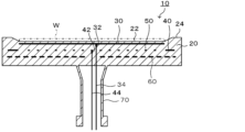
- FIG. 2 is a cross-sectional view taken along line AA in FIG. 1 .
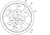
- 4 is an explanatory diagram of a first RF electrode 30 and a second RF electrode 40 with a connection circuit 50 provided inside, as viewed from above;
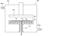
- FIG. FIG. FIG. 1 is a schematic explanatory diagram of a plasma enhanced chemical vapor deposition apparatus 80 in which a wafer stage 10 is installed.
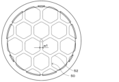
- FIG. 4 is an explanatory diagram of a comparative example of a connection circuit 50.
- FIG. 4 is an explanatory diagram of a comparative example of a connection circuit 50.
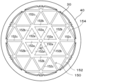
- FIG. 4 is an explanatory diagram of an embodiment of a connection circuit 150.
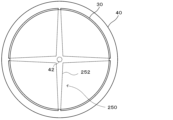
- FIG. 2 is an illustration of an embodiment of a connection circuit 250.
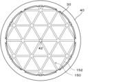
- FIG. 4 is an explanatory diagram of a comparative example of a connection circuit 150.
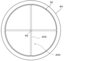
- FIG. 4 is an explanatory diagram of a comparative example of a connection circuit 250.
- Fig. 1 is a perspective view of a wafer mounting table 10
- Fig. 2 is a cross-sectional view taken along line A-A in Fig. 1
- Fig. 3 is an explanatory diagram showing a plan view of a first RF electrode 30 and a second RF electrode 40 with a connection circuit 50 provided inside
- Fig. 4 is a partially enlarged view of the connection circuit 50.
- the wafer mounting table 10 is used as a part of a device for manufacturing semiconductors, etc., and examples of such parts include an electrostatic chuck and a ceramic heater.
- the wafer mounting table 10 includes a ceramic plate 20 and a shaft 70.
- the ceramic plate 20 is a disk-shaped plate made of a ceramic material such as aluminum nitride or alumina, and has a circular wafer mounting surface 22 and an annular protrusion 24 on the upper surface.
- the diameter of the ceramic plate 20 is, for example, about 330 mm, and the thickness is, for example, about 20 mm.
- the diameter of the wafer mounting surface 22 is, for example, about 300 mm, which is approximately the same as the diameter of the wafer W.
- the annular protrusion 24 is provided so as to surround the wafer mounting surface 22 and to be one step higher than the wafer mounting surface 22.
- a first RF electrode 30, a second RF electrode 40, and a heater electrode 60 are embedded in the ceramic plate 20, in that order from the side closest to the wafer mounting surface 22.
- the first RF electrode 30 is a circular metal mesh, typically a Mo mesh or a W mesh.
- the center of the first RF electrode 30 coincides with the center of the ceramic plate 20.
- the diameter of the first RF electrode 30 is, for example, about 300 mm.
- the first RF electrode 30 is electrically connected to the first RF terminal 32 near the center of the ceramic plate 20.
- the first RF electrode 30 is connected to the first power feed rod 34 via the first RF terminal 32.
- the first power feed rod 34 penetrates the second RF electrode 40 and the heater electrode 60 in a non-contact state, passes through the inside of the shaft 70, and reaches the outside of the shaft 70.
- the second RF electrode 40 is embedded in the ceramic plate 20 at a different depth from the first RF electrode 30.
- the second RF electrode 40 is an annular metal mesh, typically a Mo mesh or a W mesh.
- the center of the second RF electrode 40 coincides with the center of the ceramic plate 20.
- the inner diameter of the second RF electrode 40 is the same as or slightly larger than the diameter of the first RF electrode 30, and the outer diameter is, for example, about 315 mm.
- the second RF electrode 40 is electrically connected to a second RF terminal 42 provided at the center of the ceramic plate 20 via a connection circuit 50.
- the second RF electrode 40 is connected to a second power supply rod 44 via the second RF terminal 42.
- the second power supply rod 44 penetrates the heater electrode 60 in a non-contact state, passes through the inside of the shaft 70, and reaches the outside of the shaft 70.
- connection circuit 50 is provided at the same depth as the second RF electrode 40 in the ceramic plate 20.
- the connection circuit 50 is provided inside the second RF electrode 40.
- the connection circuit 50 is formed of a mesh-like conductive wire 52, and has a hexagonal mesh 54.
- the center of the connection circuit 50 coincides with the center of the ceramic plate 20, and the second RF terminal 42 is electrically connected to it.
- the conductive wire 52 is preferably made of a high-melting point conductive material such as Mo, W, or Nb.
- the connection circuit 50 can be formed by printing a paste containing such a high-melting point conductive material.
- the width of the conductive wires 52 increases from the annular second RF electrode 40 toward the second RF terminal 42.
- the width of the conductive wires 52 is determined as follows. That is, an imaginary small circle C1 and an imaginary large circle C2 are drawn concentrically with the ceramic plate 20 in a plan view.
- the radius of the imaginary small circle C1 is approximately the same as the length of the sides of the hexagon that forms the mesh 54
- the radius of the imaginary large circle C2 is approximately the same as the length of the diagonal line (a diagonal line that does not pass through the center) of the hexagon that forms the mesh 54.
- the width w1 of the conductive wires 52 located inside the imaginary small circle C1 (three conductive wires 52a) is the largest
- the width w2 of the conductive wires 52 located outside the imaginary small circle C1 and inside the imaginary large circle C2 (six conductive wires 52b) is the next largest
- the width w3 of the conductive wires 52c located outside the imaginary large circle C2 is the smallest.
- the width w1 of the innermost line segment (conductive line 52a) of the conductive line 52 that is connected to the second RF terminal 42 is the widest
- the width of the remaining conductive line 52c is the narrowest. In this way, the width of the conductive line 52 increases stepwise from the annular second RF electrode 40 toward the second RF terminal 42.
- the width of the conductive wire 52 is preferably in the range of 5 mm to 15 mm, and increases from the second RF electrode 40 to the second RF terminal 42.
- w3 5 mm
- w2 10 mm
- w3 6 mm
- w2 8 mm
- w3 6 mm
- w2 7 mm
- the heater electrode 60 is formed so that it runs from one end located near the center of the ceramic plate 20 to the other end located near the center, after being wired in a single stroke across almost the entire area of the ceramic plate 20 in a plan view.
- a high melting point conductive material such as Mo, W, or Nb is preferable as the material for the heater electrode 60.
- a power supply rod is connected to each of one and the other ends of the heater electrode 60, and each power supply rod passes through the inside of the shaft 70 and is connected to a heater power source.
- the heater electrodes 60 may be provided in multiple stages, one above the other.
- the shaft 70 is a cylindrical member made of the same material as the ceramic plate 20.
- the upper end of the shaft 70 is joined to the lower surface of the ceramic plate 20 (the surface opposite the wafer mounting surface 22).
- Such a wafer mounting table 10 can be manufactured, for example, in accordance with the manufacturing example described in Patent Document 2.
- FIG. 5 is a schematic diagram of a plasma-excited chemical vapor deposition apparatus 80 in which the wafer mounting table 10 is installed.
- the wafer mounting table 10, on which the wafer W is mounted on the wafer mounting surface 22, is installed inside the chamber 82 of the plasma-excited chemical vapor deposition apparatus 80.
- the lower end of the shaft 70 is installed so as to be airtight on the floor surface of the chamber 82.
- a counter electrode 84 is provided on the ceiling of the chamber 82 at a position facing the wafer mounting table 10.
- the heater electrode 60 power is supplied to the heater electrode 60 so that the wafer W mounted on the wafer mounting table 10 is at a predetermined temperature.
- the inside of the chamber 82 is depressurized to a predetermined vacuum level by a vacuum pump connected to the gas exhaust port 82a of the chamber 82.
- a raw material gas for producing a desired film is introduced from the gas inlet 82b of the chamber 82, and the internal pressure of the chamber 82 is adjusted to a predetermined pressure.
- different high-frequency powers are supplied between the first RF electrode 30 and the counter electrode 84 and between the second RF electrode 40 and the counter electrode 84.
- plasma is generated between the counter electrode 84 and the wafer mounting table 10, and a desired thin film is formed on the surface of the wafer W.
- the connection circuit 50 connecting the second RF terminal 42 and the second RF electrode 40 is formed of mesh-like conductive wires 52 (52a to 52c), and the width of the conductive wires 52 increases from the second RF electrode 40 to the second RF terminal 42.
- the width of the conductive wires 52 is narrow at the connection portion with the second RF electrode 40 and wide at the connection portion with the second RF terminal 42. Therefore, compared to when the width of the conductive wires 52 of the connection circuit 50 is constant at a narrow value (for example, the width of the conductive wires 52 is constant at w3 as shown in FIG. 6), heat generation of the conductive wires 52 forming the connection circuit 50 can be suppressed.
- the temperature difference within the wafer mounting surface 22 can be reduced.
- the width of the conductive line 52 of the connection circuit 50 is constant at a wide value (for example, the width of the conductive line 52 is constant at w1 as shown in FIG. 7)
- the overlapping area between the first RF electrode 30 and the connection circuit 50 is smaller in a plan view, and plasma coupling between the first RF electrode 30 and the connection circuit 50 is reduced. As a result, plasma can be efficiently generated above the wafer placement surface 22.
- the second RF terminal 42 is also provided at the center of the ceramic plate 20. This makes it easy to arrange the conductive wires 52 that form the connection circuit 50 in a well-balanced manner. Specifically, it is easy to form the connection circuit 50 so that it is substantially rotationally symmetrical with the center of the ceramic plate 20 as the axis.
- the width of the conductive wires 52 is wider from the second RF electrode 40 to the second RF terminal 42 within the range of 5 mm to 15 mm. This makes it possible to appropriately reduce the overlapping area between the first RF electrode 30 and the connection circuit 50 in a plan view while appropriately suppressing heat generation in the connection circuit 50.
- connection circuit 50 has a polygonal (hexagonal) mesh 54. This makes it easier to bring the average temperature of the wafer mounting surface 22 closer to the target temperature of the wafer mounting surface 22. This point will be explained in the following example.
- connection circuit 50 having the hexagonal mesh 54 can be designed relatively easily so that the width increases from the second RF electrode 40 toward the second RF terminal 42.
- connection circuit 50 has a hexagonal mesh 54, but the mesh may be a polygon other than a hexagon.
- FIG. 8 shows an example of a connection circuit 150 having a triangular mesh 154.
- the connection circuit 150 is a circuit that connects the second RF terminal 42 and the second RF electrode 40, and overlaps with the first RF electrode 30 in a plan view.
- the width of the conductive wire 152 forming the connection circuit 150 increases from the annular second RF electrode 40 toward the second RF terminal 42.
- the width of the innermost line segment (conductive wire 152a) of the conductive wire 152 that is connected to the second RF terminal 42 is the widest
- the width of the line segment (conductive wire 152b) of the conductive wire 152 closest to the second RF terminal 42 is the next widest after the innermost line segment
- the width of the remaining conductive wire 152c is the narrowest.
- connection circuit 50 is formed of mesh-like conductive wires 52, but it may be formed of radial conductive wires.
- FIG. 9 shows an example of a connection circuit 250 formed of radial conductive wires 252.
- the connection circuit 250 is a circuit that connects the second RF terminal 42 and the second RF electrode 40, and overlaps with the first RF electrode 30 in a planar view.
- the width of the four conductive wires 252 that form the connection circuit 250 increases from the annular second RF electrode 40 toward the second RF terminal 42.
- the width of the conductive wires 252 increases gradually, not in a stepwise manner.
- the number of radial conductive wires 252 is not limited to four, and may be three, five or more.
- the width of the conductive line 52 of the connection circuit 50 is set to three stages (w1, w2, w3), but this is not particularly limited, and it may be set to, for example, two stages, or four or more stages.
- a circular electrode is used as the first RF electrode 30, but this is not particularly limited.
- the first RF electrode 30 may be a pair of semicircular electrodes arranged with a gap therebetween so as to form a substantially circular shape.
- the pair of semicircular electrodes are configured to have the same potential when high-frequency power is supplied.
- the second RF terminal 42 was connected to ground, and the difference between the maximum and minimum temperatures (hereinafter referred to as the temperature difference) in the wafer mounting surface 22 was obtained when 2000 W of power was input to the second RF electrode 40. No power was supplied to the first RF electrode 30 or the heater electrode 60. The temperature was measured at 18 predetermined points on the wafer mounting surface 22. As a result, the temperature difference was 44.3° C.
- the target temperature of the wafer mounting surface 22 was set to 300°C, and the power supply to the heater electrode 60 was controlled so that the temperature of the wafer mounting surface 22 became the target temperature.
- the second RF terminal 42 was connected to ground, and 2000 W of power was input to the second RF electrode 40. Furthermore, no power was supplied to the first RF electrode 30.
- the average temperature of the wafer mounting surface 22 at this time was determined. The temperature was measured at the same points as before. As a result, the average temperature was 306.6°C.
- Comparative Example 1 In Comparative Example 1, the connection circuit 50 shown in FIG. 6 was used, and the width w3 of the conductive line 52 was fixed at 6 mm, but other than that, the wafer mounting table 10 was the same as that of Example 1. The temperature difference and average temperature were obtained in the same manner as in Example 1. As a result, the temperature difference was 58.0°C, and the average temperature was 307.4°C.
- Example 2 In Example 2, the connection circuit 150 of Fig. 8 was used in place of the connection circuit 50 in the wafer mounting table 10 of the above embodiment, and the width of the conductive line 152a was set to 8 mm, the width of the conductive line 152b to 7 mm, and the width of the conductive line 152c to 6 mm. The temperature difference and average temperature were then determined in the same manner as in Example 1. As a result, the temperature difference was 20.4°C, and the average temperature was 310.6°C.
- Comparative Example 2 In Comparative Example 2, the connection circuit 150 shown in FIG. 10 was used, and the width of the conductive wire 152 was fixed at 6 mm, but other than that, the wafer mounting table 10 was the same as that of Example 2. The temperature difference and average temperature were obtained in the same manner as in Example 1. As a result, the temperature difference was 30.7°C, and the average temperature was 311.9°C.
- Example 3 In Example 3, the connection circuit 250 in Fig. 9 was used in place of the connection circuit 50 in the wafer mounting table 10 of the above embodiment, and the width of the conductive line 252 was set to 6 mm at the connection portion with the second RF electrode 40 and 8 mm at the connection portion with the second RF terminal 42. Then, the temperature difference and average temperature were obtained in the same manner as in Example 1. As a result, the temperature difference was 18.7°C, and the average temperature was 321.9°C.
- Comparative Example 3 In Comparative Example 3, the connection circuit 250 shown in FIG. 11 was used, and the width of the conductive wire 252 was fixed at 6 mm, but other than that, the wafer mounting table 10 was the same as that of Example 3. The temperature difference and average temperature were obtained in the same manner as in Example 1. As a result, the temperature difference was 22.1° C., and the average temperature was 324.2° C.
- the temperature difference was smaller in Examples 1 to 3 than in the corresponding Comparative Examples 1 to 3. That is, the temperature difference could be reduced when the width of the conductive wire constituting the connection circuit was wider from the second RF electrode to the second RF terminal than when the width was constant at a narrow value. Also, the average temperature could be closer to the target temperature (300° C.) when the connection circuit was formed of mesh-like conductive wires as in Examples 1 and 2 than when the connection circuit was formed of radial conductive wires as in Example 3.
- the present invention can be used as a component in semiconductor manufacturing equipment.
- 10 wafer placement table 20 ceramic plate, 22 wafer placement surface, 24 protrusion, 30 first RF electrode, 32 first RF terminal, 34 first power feed rod, 40 second RF electrode, 42 second RF terminal, 44 second power feed rod, 50 connection circuit, 52, 52a, 52b, 52c conductive wire, 54 mesh, 60 heater electrode, 70 shaft, 80 plasma enhanced chemical vapor deposition apparatus, 82 chamber, 82a gas exhaust port, 82b gas inlet port, 84 counter electrode, 150 connection circuit, 152, 152a, 152b, 152c conductive wire, 250 connection circuit, 252 conductive wire, C1 imaginary small circle, C2 imaginary large circle, W wafer, w1, w2, w3 width.
Landscapes
- Chemical & Material Sciences (AREA)
- Engineering & Computer Science (AREA)
- Physics & Mathematics (AREA)
- Plasma & Fusion (AREA)
- Analytical Chemistry (AREA)
- Chemical Kinetics & Catalysis (AREA)
- General Chemical & Material Sciences (AREA)
- Materials Engineering (AREA)
- Mechanical Engineering (AREA)
- Metallurgy (AREA)
- Organic Chemistry (AREA)
- Container, Conveyance, Adherence, Positioning, Of Wafer (AREA)
- Drying Of Semiconductors (AREA)
- Chemical Vapour Deposition (AREA)
Abstract
Description
上面にウエハ載置面を有するセラミックプレートと、
前記セラミックプレートに埋設された円形の第1RF電極と、
前記第1RF電極に電気的に接続される第1RF端子と、
前記セラミックプレートのうち前記第1RF電極とは異なる深さに埋設され、平面視で前記第1RF電極の外側に位置する環状の第2RF電極と、
前記第2RF電極に電気的に接続される第2RF端子と、
前記第2RF端子と前記第2RF電極とを接続する接続回路と、
を備え、
前記接続回路は、網目状又は放射状の導電線で形成され、
前記導電線の幅は、前記第2RF電極から前記第2RF端子に向かって広くなっている
ものである。
実施例1では、上述した実施形態のウエハ載置台10(図1~図4)においてw1=8mm、w2=7mm、w3=6mmに設定した。そして、第2RF端子42をグランドに接続し、第2RF電極40に2000Wの電力を入力したときのウエハ載置面22内の最高温度と最低温度との差(以下温度差という)を求めた。第1RF電極30やヒータ電極60には電力を供給しなかった。温度の測定点は、ウエハ載置面22において予め定めた18箇所とした。その結果、温度差は44.3℃であった。
比較例1では、接続回路50として図6を採用し、導電線52の幅w3を6mmで一定とした以外は、実施例1のウエハ載置台10と同様とした。そして、実施例1と同様にして温度差及び平均温度を求めた。その結果、温度差は58.0℃、平均温度は307.4℃であった。
実施例2では、上述した実施形態のウエハ載置台10において接続回路50の代わりに図8の接続回路150を用い、導電線152aの幅を8mm、導電線152bの幅を7mm、導電線152cの幅を6mmに設定した。そして、実施例1と同様にして温度差及び平均温度を求めた。その結果、温度差は20.4℃、平均温度は310.6℃であった。
比較例2では、接続回路150として図10を採用し、導電線152の幅を6mmで一定とした以外は、実施例2のウエハ載置台10と同様とした。そして、実施例1と同様にして温度差及び平均温度を求めた。その結果、温度差は30.7℃、平均温度は311.9℃であった。
実施例3では、上述した実施形態のウエハ載置台10において接続回路50の代わりに図9の接続回路250を用い、導電線252の幅を、第2RF電極40との接続部分で6mm、第2RF端子42との接続部分で8mmに設定した。そして、実施例1と同様にして温度差及び平均温度を求めた。その結果、温度差は18.7℃、平均温度は321.9℃であった。
比較例3では、接続回路250として図11を採用し、導電線252の幅を6mmで一定とした以外は、実施例3のウエハ載置台10と同様とした。そして、実施例1と同様にして温度差及び平均温度を求めた。その結果、温度差は22.1℃、平均温度は324.2℃であった。
温度差については、実施例1~3の方がそれぞれ対応する比較例1~3に比べて小さくなった。すなわち、接続回路を構成する導電線の幅については、第2RF電極から第2RF端子に向かって広くなっている方が、狭い値で一定の場合に比べて、温度差を小さくすることができた。また、平均温度については、実施例1,2のように接続回路が網目状の導電線で形成されている方が、実施例3のように放射状の導電線で形成されている場合に比べて目標温度(300℃)に近づけることができた。
Claims (5)
- 上面にウエハ載置面を有するセラミックプレートと、
前記セラミックプレートに埋設された円形の第1RF電極と、
前記第1RF電極に電気的に接続される第1RF端子と、
前記セラミックプレートのうち前記第1RF電極とは異なる深さに埋設され、平面視で前記第1RF電極の外側に位置する環状の第2RF電極と、
前記第2RF電極に電気的に接続される第2RF端子と、
前記第2RF端子と前記第2RF電極とを接続する接続回路と、
を備え、
前記接続回路は、網目状又は放射状の導電線で形成され、
前記導電線の幅は、前記第2RF電極から前記第2RF端子に向かって広くなっている、
ウエハ載置台。 - 前記第2RF端子は、前記セラミックプレートの中心に設けられている、
請求項1に記載のウエハ載置台。 - 前記導電線の幅は、5mm以上15mm以下の範囲内で前記第2RF電極から前記第2RF端子に向かって広くなっている、
請求項1又は2に記載のウエハ載置台。 - 前記接続回路は、前記網目状の導電線で形成され、多角形の網目を有する、
請求項1又は2に記載のウエハ載置台。 - 前記導電線のうち前記第2RF端子と繋がっている最内周線分の幅が最も広く、前記導電線のうち前記最内周線分の次に前記第2RF端子に近い線分の幅が次に広くなっている、
請求項4に記載のウエハ載置台。
Priority Applications (6)
| Application Number | Priority Date | Filing Date | Title |
|---|---|---|---|
| KR1020237020339A KR102739442B1 (ko) | 2023-01-12 | 2023-01-12 | 웨이퍼 적재대 |
| CN202380008744.5A CN120500743A (zh) | 2023-01-12 | 2023-01-12 | 晶片载放台 |
| PCT/JP2023/000526 WO2024150352A1 (ja) | 2023-01-12 | 2023-01-12 | ウエハ載置台 |
| JP2023533323A JP7529912B1 (ja) | 2023-01-12 | 2023-01-12 | ウエハ載置台 |
| US18/332,922 US12573598B2 (en) | 2023-01-12 | 2023-06-12 | Wafer placement table |
| TW112134616A TW202429621A (zh) | 2023-01-12 | 2023-09-12 | 晶圓載置台 |
Applications Claiming Priority (1)
| Application Number | Priority Date | Filing Date | Title |
|---|---|---|---|
| PCT/JP2023/000526 WO2024150352A1 (ja) | 2023-01-12 | 2023-01-12 | ウエハ載置台 |
Related Child Applications (1)
| Application Number | Title | Priority Date | Filing Date |
|---|---|---|---|
| US18/332,922 Continuation US12573598B2 (en) | 2023-01-12 | 2023-06-12 | Wafer placement table |
Publications (1)
| Publication Number | Publication Date |
|---|---|
| WO2024150352A1 true WO2024150352A1 (ja) | 2024-07-18 |
Family
ID=91854990
Family Applications (1)
| Application Number | Title | Priority Date | Filing Date |
|---|---|---|---|
| PCT/JP2023/000526 Ceased WO2024150352A1 (ja) | 2023-01-12 | 2023-01-12 | ウエハ載置台 |
Country Status (6)
| Country | Link |
|---|---|
| US (1) | US12573598B2 (ja) |
| JP (1) | JP7529912B1 (ja) |
| KR (1) | KR102739442B1 (ja) |
| CN (1) | CN120500743A (ja) |
| TW (1) | TW202429621A (ja) |
| WO (1) | WO2024150352A1 (ja) |
Citations (5)
| Publication number | Priority date | Publication date | Assignee | Title |
|---|---|---|---|---|
| JP2010258428A (ja) * | 2009-03-30 | 2010-11-11 | Tokyo Electron Ltd | プラズマ処理装置及びプラズマ処理方法 |
| WO2014073554A1 (ja) * | 2012-11-06 | 2014-05-15 | 日本碍子株式会社 | サセプタ |
| WO2018179891A1 (ja) * | 2017-03-28 | 2018-10-04 | 住友電気工業株式会社 | ウエハ保持体 |
| JP2019522374A (ja) * | 2016-07-22 | 2019-08-08 | アプライド マテリアルズ インコーポレイテッドApplied Materials,Incorporated | 半導体及び機械処理におけるワークピースキャリアの上板としての処理済みウエハ |
| JP2022534141A (ja) * | 2018-10-12 | 2022-07-28 | アプライド マテリアルズ インコーポレイテッド | ヒータが一体化されたチャンバリッド |
Family Cites Families (12)
| Publication number | Priority date | Publication date | Assignee | Title |
|---|---|---|---|---|
| JPS5583877U (ja) | 1978-12-05 | 1980-06-10 | ||
| US5968379A (en) * | 1995-07-14 | 1999-10-19 | Applied Materials, Inc. | High temperature ceramic heater assembly with RF capability and related methods |
| US6616767B2 (en) * | 1997-02-12 | 2003-09-09 | Applied Materials, Inc. | High temperature ceramic heater assembly with RF capability |
| JP3359582B2 (ja) * | 1998-11-27 | 2002-12-24 | 京セラ株式会社 | 静電チャック |
| JP2002313899A (ja) * | 2001-04-11 | 2002-10-25 | Sumitomo Electric Ind Ltd | 基板保持構造体および基板処理装置 |
| US7712434B2 (en) * | 2004-04-30 | 2010-05-11 | Lam Research Corporation | Apparatus including showerhead electrode and heater for plasma processing |
| JP5896595B2 (ja) | 2010-10-20 | 2016-03-30 | ラム リサーチ コーポレーションLam Research Corporation | 2層rf構造のウエハ保持体 |
| JP2012182221A (ja) * | 2011-02-28 | 2012-09-20 | Taiheiyo Cement Corp | 基板支持部材 |
| JP6077258B2 (ja) * | 2012-10-05 | 2017-02-08 | 日本特殊陶業株式会社 | 積層発熱体、静電チャック、及びセラミックヒータ |
| US9460950B2 (en) * | 2013-12-06 | 2016-10-04 | Applied Materials, Inc. | Wafer carrier for smaller wafers and wafer pieces |
| US20230290611A1 (en) * | 2020-05-27 | 2023-09-14 | Lam Research Corporation | Distributed plasma source array |
| KR102259949B1 (ko) * | 2020-09-09 | 2021-06-02 | 주식회사 미코세라믹스 | 서셉터 및 그 제조 방법 |
-
2023
- 2023-01-12 JP JP2023533323A patent/JP7529912B1/ja active Active
- 2023-01-12 CN CN202380008744.5A patent/CN120500743A/zh active Pending
- 2023-01-12 KR KR1020237020339A patent/KR102739442B1/ko active Active
- 2023-01-12 WO PCT/JP2023/000526 patent/WO2024150352A1/ja not_active Ceased
- 2023-06-12 US US18/332,922 patent/US12573598B2/en active Active
- 2023-09-12 TW TW112134616A patent/TW202429621A/zh unknown
Patent Citations (5)
| Publication number | Priority date | Publication date | Assignee | Title |
|---|---|---|---|---|
| JP2010258428A (ja) * | 2009-03-30 | 2010-11-11 | Tokyo Electron Ltd | プラズマ処理装置及びプラズマ処理方法 |
| WO2014073554A1 (ja) * | 2012-11-06 | 2014-05-15 | 日本碍子株式会社 | サセプタ |
| JP2019522374A (ja) * | 2016-07-22 | 2019-08-08 | アプライド マテリアルズ インコーポレイテッドApplied Materials,Incorporated | 半導体及び機械処理におけるワークピースキャリアの上板としての処理済みウエハ |
| WO2018179891A1 (ja) * | 2017-03-28 | 2018-10-04 | 住友電気工業株式会社 | ウエハ保持体 |
| JP2022534141A (ja) * | 2018-10-12 | 2022-07-28 | アプライド マテリアルズ インコーポレイテッド | ヒータが一体化されたチャンバリッド |
Also Published As
| Publication number | Publication date |
|---|---|
| TW202429621A (zh) | 2024-07-16 |
| US12573598B2 (en) | 2026-03-10 |
| US20240242943A1 (en) | 2024-07-18 |
| KR20240113702A (ko) | 2024-07-23 |
| KR102739442B1 (ko) | 2024-12-10 |
| CN120500743A (zh) | 2025-08-15 |
| JPWO2024150352A1 (ja) | 2024-07-18 |
| JP7529912B1 (ja) | 2024-08-06 |
Similar Documents
| Publication | Publication Date | Title |
|---|---|---|
| JP5583877B1 (ja) | サセプタ | |
| US11764039B2 (en) | Wafer support | |
| US11756806B2 (en) | Heater power feeding mechanism | |
| US11756807B2 (en) | Power feeding mechanism and method for controlling temperature of a stage | |
| JP5606565B2 (ja) | 容積可変型プラズマ処理チャンバおよびその方法 | |
| US8314560B2 (en) | Plasma processing apparatus | |
| TWI673823B (zh) | 陶瓷加熱器和具有增強的晶片邊緣效能的esc | |
| CN106463449B (zh) | 具有凸起的顶板及冷却通道的静电夹盘 | |
| US10755902B2 (en) | Plasma processing apparatus and focus ring | |
| CN111048394A (zh) | 等离子体处理装置 | |
| CN1675737A (zh) | 电极同时响应于多频的等离子体处理器 | |
| JP2018190978A (ja) | 対称的な給電構造を有する補助電極を用いてプラズマ処理チャンバ内のウェハエッジシースを変調する方法および受動的な方法で動作するとき制御可能なインピーダンスを接地し、能動的に電力を供給するときプラズマへの対称rf電力入力を可能とするドライブ | |
| JP2018110216A (ja) | プラズマ処理装置 | |
| JP6289860B2 (ja) | プラズマエッチングチャンバ用のtcctマッチング回路 | |
| JP7740240B2 (ja) | ウエハ支持装置 | |
| JP2023527988A (ja) | 分散型プラズマ源アレイ | |
| WO2023175690A1 (ja) | プラズマ処理装置 | |
| JP7529912B1 (ja) | ウエハ載置台 | |
| US20220172926A1 (en) | Plasma processing apparatus and method for fabricating semiconductor device using the same | |
| TWI731994B (zh) | 用於介電蝕刻腔室之腔室填充物套組 | |
| WO2018230232A1 (ja) | ウエハ加熱ヒータ及び半導体製造装置 | |
| US10892142B2 (en) | System for fabricating a semiconductor device | |
| US20250201538A1 (en) | Esc design with enhanced tunability for wafer far edge plasma profile control | |
| KR20070050111A (ko) | 균일한 온도제어를 위한 정전척 및 이를 포함하는 플라즈마발생장치 | |
| TWI415526B (zh) | 電漿處理裝置 |
Legal Events
| Date | Code | Title | Description |
|---|---|---|---|
| WWE | Wipo information: entry into national phase |
Ref document number: 202380008744.5 Country of ref document: CN |
|
| WWE | Wipo information: entry into national phase |
Ref document number: 2023533323 Country of ref document: JP |
|
| 121 | Ep: the epo has been informed by wipo that ep was designated in this application |
Ref document number: 23915974 Country of ref document: EP Kind code of ref document: A1 |
|
| NENP | Non-entry into the national phase |
Ref country code: DE |
|
| WWP | Wipo information: published in national office |
Ref document number: 202380008744.5 Country of ref document: CN |
|
| 122 | Ep: pct application non-entry in european phase |
Ref document number: 23915974 Country of ref document: EP Kind code of ref document: A1 |