WO2024147269A1 - 半導体装置 - Google Patents
半導体装置 Download PDFInfo
- Publication number
- WO2024147269A1 WO2024147269A1 PCT/JP2023/044791 JP2023044791W WO2024147269A1 WO 2024147269 A1 WO2024147269 A1 WO 2024147269A1 JP 2023044791 W JP2023044791 W JP 2023044791W WO 2024147269 A1 WO2024147269 A1 WO 2024147269A1
- Authority
- WO
- WIPO (PCT)
- Prior art keywords
- semiconductor device
- semiconductor chip
- thickness direction
- pair
- thickness
- Prior art date
- Legal status (The legal status is an assumption and is not a legal conclusion. Google has not performed a legal analysis and makes no representation as to the accuracy of the status listed.)
- Ceased
Links
Images


Classifications
-
- H—ELECTRICITY
- H10—SEMICONDUCTOR DEVICES; ELECTRIC SOLID-STATE DEVICES NOT OTHERWISE PROVIDED FOR
- H10W—GENERIC PACKAGES, INTERCONNECTIONS, CONNECTORS OR OTHER CONSTRUCTIONAL DETAILS OF DEVICES COVERED BY CLASS H10
- H10W72/00—Interconnections or connectors in packages
-
- H—ELECTRICITY
- H10—SEMICONDUCTOR DEVICES; ELECTRIC SOLID-STATE DEVICES NOT OTHERWISE PROVIDED FOR
- H10W—GENERIC PACKAGES, INTERCONNECTIONS, CONNECTORS OR OTHER CONSTRUCTIONAL DETAILS OF DEVICES COVERED BY CLASS H10
- H10W72/00—Interconnections or connectors in packages
- H10W72/071—Connecting or disconnecting
Definitions
- an object A is located on (an object B) includes “an object A is in contact with an object B and is located on (an object B)” and “an object A is located on (an object B) with another object interposed between the object A and the object B".
- an object A overlaps an object B includes “an object A overlaps the entire object B” and “an object A overlaps a part of an object B” unless otherwise specified.
- an object A (its material) contains a certain material C includes “an object A (its material) is made of a certain material C” and "an object A (its material) is mainly composed of a certain material C.”
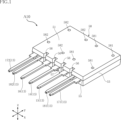
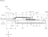
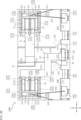
- First embodiment: 1 to 19 show a semiconductor device A10 according to a first embodiment.
- the semiconductor device A10 includes two die pads 10A, 10B, a plurality of terminal leads 13, two semiconductor chips 21, 22, two plate-shaped conductive members 31, 32, a plurality of connection members 41A, 41B, 42A, 42B, and a sealing resin 50.
- the plurality of terminal leads 13 includes a plurality of leads 14, 15, 16, 171, 172, 181, 182.
- the two die pads 10A, 10B are spaced apart from each other in the first direction x, as shown in Figures 3 and 9.
- the two die pads 10A, 10B are formed from the same lead frame together with the multiple terminal leads 13.
- the lead frame is copper (Cu) or a copper alloy. Therefore, the composition of each of the two die pads 10A, 10B and the multiple terminal leads 13 includes copper. Note that the composition of each of the two die pads 10A, 10B and the multiple terminal leads 13 may include other metals instead of copper.
- Each of the two die pads 10A, 10B is, for example, rectangular in plan view.
- the two die pads 10A and 10B each have a main surface 101 and a back surface 102.
- the main surface 101 and the back surface 102 described below are common to the two die pads 10A and 10B unless otherwise specified.
- the main surface 101 faces the thickness direction z (upward).
- the main surface 101 is covered with sealing resin 50.
- the semiconductor chip 21 is mounted on the main surface 101 of the die pad 10A.
- the back surface 102 of the die pad 10A faces the opposite side to the side where the semiconductor chip 21 is located in the thickness direction z.
- the semiconductor chip 22 is mounted on the main surface 101 of the die pad 10B.
- the back surface 102 of the die pad 10B faces the opposite side to the side where the semiconductor chip 22 is located in the thickness direction z.
- the back surface 102 is exposed from the sealing resin 50.
- the back surface 102 is plated with, for example, tin (Sn).
- the sealing resin 50 covers the two semiconductor chips 21, 22, the two plate-shaped conductive members 31, 32, and a portion of each of the two die pads 10A, 10B.
- the sealing resin 50 also covers a portion of each of the multiple terminal leads 13.
- the sealing resin 50 has electrical insulation properties.
- the sealing resin 50 contains, for example, a black epoxy resin.
- the dimension L1 of the sealing resin 50 in the first direction x is longer than the dimension L2 of the sealing resin 50 in the second direction y.
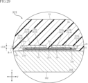
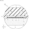
- the sealing resin 50 has a resin main surface 51, a resin back surface 52, multiple side surfaces 53, 54, 55, multiple recesses 56, a groove portion 57, and multiple recesses 581, 582.
- the pair of side surfaces 53 are spaced apart from each other in the first direction x.
- the pair of side surfaces 53 face the first direction x and extend in the second direction y.
- the pair of side surfaces 53 are connected to the resin main surface 51 and the resin back surface 52.
- the groove portion 57 is recessed from the resin back surface 52 in the thickness direction z and extends along the second direction y. Both sides of the groove portion 57 in the second direction y are connected to the two side surfaces 54, 55, respectively. When viewed in the thickness direction z, the groove portion 57 separates the back surface 102 of the die pad 10A from the back surface 102 of the die pad 10B.
- each of the multiple recesses 581, 582 does not overlap any of the two plate-shaped conductive members 31, 32 in planar view, as shown in FIG. 3. Further, as shown in FIG. 3, each of the plurality of recesses 581 and 582 does not overlap any of the plurality of connection members 41A, 41B, 42A, and 42B in a plan view.
- the plurality of recesses 581 are formed by pins for fixing the die pad 10A during the manufacture of the semiconductor device A10. The pins are pressed against the die pad 10A and fix the die pad 10A at a stage before the formation of the sealing resin 50. In this state, the formation of the sealing resin 50 is started. Then, the pins are pulled out before the formation of the sealing resin 50 is completed.
- the sealing resin 50 is formed in at least a part of the region where the pins were arranged, so that the main surface 101 of the die pad 10A is covered with the sealing resin 50.
- the plurality of recesses 581 are marks formed by such a molding process of the sealing resin 50.
- the plurality of recesses 582 are also formed by pins for fixing the die pad 10B during the manufacture of the semiconductor device A10.
- the multiple recesses 582 are marks formed during the molding process of the sealing resin 50.
- the two die pads 10A, 10B each have a plurality of end faces 111-114.
- the plurality of end faces 111-114 are covered with the sealing resin 50.
- the end face 111 faces in the first direction x and extends in the second direction y.
- the end face 111 is located closest to a pair of side faces 53 of the sealing resin 50.
- the end face 112 faces in the second direction y and extends in the first direction x.
- the end face 112 is located closest to the side face 54 of the sealing resin 50.
- the end face 113 faces the opposite side to the end face 112 in the second direction y and extends in the first direction x.
- the end face 113 is located closest to the side face 55 of the sealing resin 50.
- the end face 114 faces the opposite side to the end face 111 in the first direction x and extends in the second direction y. As shown in FIG. 9, a groove portion 57 is located between the end surface 114 of the die pad 10A and the end surface 114 of the die pad 10B.
- the distance P2 between the end face 113 and the side face 55 is longer than the distance P1 between the end face 112 and the side face 54.
- the longest normal of the corner end face 121 is set as follows.
- the longest normal is the maximum value of the normal of the corner end face 121 from the corner end face 121 of either of the two die pads 10A, 10B to the side face 53 of the pair of side faces 53 of the sealing resin 50 that is located closest to the corner end face 121.
- the longest normal is 1.0 to 1.5 times the length of the intersection line between the corner end face 121 and a virtual plane with the first direction x and the second direction y as in-plane directions.
- each of the two die pads 10A and 10B has a corner end surface 122.
- the corner end surface 122 is located between the two end surfaces 111 and 113, and is located at one of the corners of the two die pads 10A and 10B.
- the corner end surface 122 is covered with the sealing resin 50 and is a plane inclined with respect to the two end surfaces 111 and 113. Either the inclination angle of the corner end surface 122 with respect to the end surface 111 or the inclination angle of the corner end surface 122 with respect to the end surface 113 is, for example, 60° or more and 85° or less.
- One of the multiple recesses 581 is located near the corner end surface 122 of the die pad 10A in a plan view
- one of the multiple recesses 582 is located near the corner end surface 122 of the die pad 10B in a plan view.
- each of the two die pads 10A and 10B has a corner end surface 123.
- the corner end surface 123 is located between the two end surfaces 112 and 114, and is located at one of the corners of the two die pads 10A and 10B.
- the corner end surface 123 is covered with the sealing resin 50 and is a plane inclined with respect to the two end surfaces 112 and 114. Either the inclination angle of the corner end surface 123 with respect to the end surface 114 or the inclination angle of the corner end surface 123 with respect to the end surface 112 is, for example, 60° or more and 85° or less.
- One of the multiple recesses 581 is located near the corner end surface 123 of the die pad 10A in a plan view
- one of the multiple recesses 582 is located near the corner end surface 123 of the die pad 10B in a plan view.
- each of the two die pads 10A and 10B has a corner end surface 124.
- the corner end surface 124 is located between the two end surfaces 113 and 114, and is located at one of the corners of the two die pads 10A and 10B.
- the corner end surface 124 is covered with the sealing resin 50 and is a plane inclined with respect to the two end surfaces 113 and 114. Either the inclination angle of the corner end surface 124 with respect to the end surface 114 or the inclination angle of the corner end surface 124 with respect to the end surface 113 is, for example, 60° or more and 85° or less.
- One of the multiple recesses 581 is located near the corner end surface 124 of the die pad 10A in a plan view
- one of the multiple recesses 582 is located near the corner end surface 124 of the die pad 10B in a plan view.
- the die pad 10B has a seating surface 103 and an upright surface 104.
- the seating surface 103 faces the same side as the main surface 101 in the thickness direction z, and is located between the main surface 101 and the back surface 102 in the thickness direction z.
- the seating surface 103 is connected to the end surface 114.
- the upright surface 104 faces in a direction perpendicular to the thickness direction z, and is connected to the seating surface 103 and the main surface 101.
- the seating surface 103 and the upright surface 104 form a step in the die pad 10B.
- Each of the two semiconductor chips 21, 22 is, for example, a transistor.
- the transistor in the semiconductor device A10 is a MOSFET (Metal-Oxide-Semiconductor Field-Effect Transistor), but may also be a bipolar transistor or an IGBT (Insulated Gate Bipolar Transistor).
- the circuit in FIG. 19 also illustrates a parasitic diode component built into each of the two semiconductor chips 21, 22.
- Each of the two semiconductor chips 21, 22 is, for example, an n-channel type, but may also be a p-channel type.
- Each of the two semiconductor chips 21, 22 includes a compound semiconductor substrate.
- the composition of the compound semiconductor substrate includes silicon (Si) or silicon carbide (SiC).
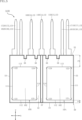
- the semiconductor chip 21 is mounted on the die pad 10A as shown in Figures 3, 4 and 9.
- the center of gravity of the semiconductor chip 21 overlaps with the center of the die pad 10A.
- the center of the die pad 10A is the center when the die pad 10A is divided into Nx (Nx is a positive odd number) in the first direction x, and is the region that corresponds to the center when the die pad 10A is divided into Ny (Ny is a positive odd number) in the second direction y.
- Nx and Ny are not limited in any way, but are, for example, 3 or 5.
- the semiconductor chip 21 has a main surface 21a and a back surface 21b. As shown in FIG. 10, the main surface 21a and the back surface 21b are spaced apart from each other in the thickness direction z.
- the main surface 21a faces in the same direction as the main surface 101 of the die pad 10A.
- the back surface 21b faces the opposite side to the main surface 21a in the thickness direction z and faces the main surface 101 of the die pad 10A.
- the semiconductor chip 21 is rectangular in plan view. Therefore, the outer periphery 219 (see Figure 4) of the semiconductor chip 21 in plan view is rectangular.
- the outer periphery 219 has a pair of edges 219a and a pair of edges 219b. As shown in Figure 4, the pair of edges 219a are spaced apart in the second direction y and extend in the first direction x in plan view. The pair of edges 219a are parallel to each other. The pair of edges 219b are spaced apart in the first direction x and extend in the second direction y in plan view. The pair of edges 219b are parallel to each other.
- the semiconductor chip 21 is mounted on the die pad 10A. As shown in Figures 4 and 10, the semiconductor chip 21 has a number of main surface electrodes 211, 212, 214 and a back surface electrode 213.
- the principal surface electrode 211 is disposed on the principal surface 21a. A current corresponding to the power converted by the semiconductor chip 21 flows through the principal surface electrode 211.
- the principal surface electrode 211 is, for example, a source electrode.
- the principal surface electrode 211 includes a plurality of metal plating layers.
- the principal surface electrode 211 includes a nickel (Ni) plating layer and a gold (Au) plating layer laminated on the nickel plating layer.
- the principal surface electrode 211 may include a nickel plating layer, a palladium (Pd) plating layer laminated on the nickel plating layer, and a gold plating layer laminated on the palladium plating layer.
- the principal surface electrode 212 is disposed on the principal surface 21a.
- a drive signal (gate voltage) for driving the semiconductor chip 21 is applied to the principal surface electrode 212.
- the principal surface electrode 212 is, for example, a gate electrode.
- the area of the principal surface electrode 212 is smaller than the area of the principal surface electrode 211.
- the principal surface electrode 212 is located on the side closer to the end surface 111 of the die pad 10A than the principal surface electrode 211 in the first direction x.
- the pair of principal surface electrodes 214 are disposed on the principal surface 21a.
- the pair of principal surface electrodes 214 are at the same potential as the principal surface electrode 211.
- the pair of principal surface electrodes 214 are source sense electrodes.
- the pair of principal surface electrodes 214 are disposed on both sides of the principal surface electrode 212 in the second direction y in a plan view. In a plan view, the area of the principal surface electrode 214 is smaller than the area of the principal surface electrode 211.
- the pair of principal surface electrodes 214 are positioned closer to the end surface 111 of the die pad 10A in the first direction x than the principal surface electrode 211.
- the semiconductor chip 21 may have only one of the pair of principal surface electrodes 214, or may have neither of the pair of principal surface electrodes 214.
- the back electrode 213 is disposed on the back surface 21b.
- the back electrode 213 is provided facing the main surface 101 of the die pad 10A.
- a current corresponding to the power before being converted by the semiconductor chip 21 flows through the back electrode 213.
- the back electrode 213 is, for example, a drain electrode.
- the semiconductor chip 22 is mounted on the main surface 101 of the die pad 10B as shown in Figures 3, 4 and 9.
- the center of gravity of the semiconductor chip 22 overlaps with the center of the die pad 10B.
- the center of the die pad 10B is the center when the die pad 10B is divided into Lx (Lx is a positive odd number) in the first direction x, and is the region that corresponds to the center when the die pad 10B is divided into Ly (Ly is a positive odd number) in the second direction y.
- Lx and Ly are not limited in any way, but are, for example, 3 or 5.
- the semiconductor chip 22 has a main surface 22a and a back surface 22b. As shown in FIG. 11, the main surface 22a and the back surface 22b are spaced apart from each other in the thickness direction z.
- the main surface 22a faces in the same direction as the main surface 101 of the die pad 10B.
- the back surface 22b faces the opposite side to the main surface 22a in the thickness direction z and faces the main surface 101 of the die pad 10B.
- the semiconductor chip 22 is rectangular in plan view. Therefore, the outer periphery 229 (see Figure 4) of the semiconductor chip 22 in plan view is rectangular.
- the outer periphery 229 has a pair of edges 229a and a pair of edges 229b. As shown in Figure 4, the pair of edges 229a are spaced apart in the second direction y and extend in the first direction x in plan view. The pair of edges 229a are parallel to each other. The pair of edges 229b are spaced apart in the first direction x and extend in the second direction y in plan view. The pair of edges 229b are parallel to each other.
- the semiconductor chip 22 is mounted on the die pad 10B. As shown in Figures 4 and 11, the semiconductor chip 22 has a plurality of main surface electrodes 221, 222, and 224 and a back surface electrode 223.
- the principal surface electrode 221 is disposed on the principal surface 22a. A current corresponding to the power converted by the semiconductor chip 22 flows through the principal surface electrode 221.
- the principal surface electrode 221 is, for example, a source electrode.
- the principal surface electrode 221 includes multiple metal plating layers, similar to the principal surface electrode 211.
- the principal surface electrode 221 includes a nickel (Ni) plating layer and a gold (Au) plating layer laminated on the nickel plating layer.
- the principal surface electrode 221 may include a nickel plating layer, a palladium (Pd) plating layer laminated on the nickel plating layer, and a gold plating layer laminated on the palladium plating layer.
- the principal surface electrode 222 is disposed on the principal surface 22a.
- a drive signal (gate voltage) for driving the semiconductor chip 22 is applied to the principal surface electrode 222.
- the principal surface electrode 222 is, for example, a gate electrode.
- the area of the principal surface electrode 222 is smaller than the area of the principal surface electrode 221.
- the principal surface electrode 222 is located on the side closer to the end surface 111 of the die pad 10B than the principal surface electrode 221 in the first direction x.
- the pair of principal surface electrodes 224 are each disposed on the principal surface 22a.
- the pair of principal surface electrodes 224 are each at the same potential as the principal surface electrode 211.
- the pair of principal surface electrodes 224 are each a source sense electrode.
- the pair of principal surface electrodes 224 are disposed on both sides of the principal surface electrode 222 in the second direction y in a plan view. In a plan view, the area of the principal surface electrode 224 is smaller than the area of the principal surface electrode 221.
- the pair of principal surface electrodes 224 are each located on the side closer to the end surface 111 of the die pad 10B in the first direction x than the principal surface electrode 221.
- the semiconductor chip 22 may have only one of the pair of principal surface electrodes 224, or may have neither of the pair of principal surface electrodes 224.
- the back electrode 223 is disposed on the back surface 22b.
- the back electrode 223 is provided facing the main surface 101 of the die pad 10B.
- a current corresponding to the power before being converted by the semiconductor chip 22 flows through the back electrode 223.
- the back electrode 223 is, for example, a drain electrode.
- the semiconductor device A10 further includes two die bonding layers 231, 232.
- Each of the two die bonding layers 231, 232 is conductive.
- Each of the die bonding layers 231, 232 is, for example, solder.
- each of the die bonding layers 231, 232 may be a sintered metal.
- the die bonding layer 231 is interposed between the main surface 101 of the die pad 10A and the back electrode 213 of the semiconductor chip 21.
- the die bonding layer 231 bonds the main surface 101 of the die pad 10A and the back electrode 213 of the semiconductor chip 21. This allows the back electrode 213 of the semiconductor chip 21 to be electrically connected to the die pad 10A.
- the die bonding layer 232 is interposed between the main surface 101 of the die pad 10B and the back electrode 223 of the semiconductor chip 22.
- the die bonding layer 232 joins the main surface 101 of the die pad 10B and the back electrode 223 of the semiconductor chip 22.
- the back electrode 223 of the semiconductor chip 22 is electrically connected to the die pad 10B.
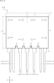
- the multiple terminal leads 13 are located on the side opposite to the side where the end face 112 faces the two die pads 10A, 10B in the second direction y. At least one of the multiple terminal leads 13 is electrically connected to one of the two semiconductor chips 21, 22.
- the multiple terminal leads 13 are arranged along the first direction x. As described above, the multiple terminal leads 13 include multiple leads 14, 15, 16, 171, 172, 181, and 182.
- the lead 14 is located away from the two die pads 10A and 10B in the second direction y, and is located between the lead 15 and the lead 16 in the first direction x.
- the lead 14 extends along the second direction y.
- the lead 14 is electrically connected to the main surface electrode 221 of the semiconductor chip 22.
- the lead 14 is an N terminal (negative electrode) to which a DC power supply voltage to be converted is applied.
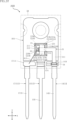
- the lead 14 includes a covering portion 14A and an exposed portion 14B. As shown in FIG. 3 and FIG. 15, the covering portion 14A is covered with the sealing resin 50.
- the exposed portion 14B is connected to the covering portion 14A and is exposed from the side 55 of the sealing resin 50.
- the exposed portion 14B extends away from the two die pads 10A and 10B in the second direction y.
- the surface of the exposed portion 14B is, for example, tin-plated.
- the covering portion 14A of the lead 14 has a seating surface 14C and an upright surface 14D.
- the seating surface 14C faces the same side in the thickness direction z as the main surfaces 101 of the two die pads 10A, 10B, and is located lower in the thickness direction z than the upper surface of the covering portion 14A (the surface facing upward in the thickness direction z).
- the upright surface 14D faces in a direction perpendicular to the thickness direction z, and is connected to the seating surface 14C and the upper surface of the covering portion 14A.
- the seating surface 14C and the upright surface 14D form a step in the covering portion 14A of the lead 14.
- the lead 15 includes a portion extending along the second direction y and is connected to the die pad 10A. Therefore, the lead 15 is electrically connected to the back electrode 213 of the semiconductor chip 21 via the die pad 10A.
- the lead 15 is a P terminal (positive electrode) to which the DC power supply voltage to be converted is applied.
- the lead 15 includes a covering portion 15A and an exposed portion 15B. As shown in FIG. 3 and FIG. 13, the covering portion 15A is connected to the end surface 113 of the die pad 10A and is covered with the sealing resin 50. When viewed in the first direction x, the covering portion 15A is bent. As shown in FIG. 2, FIG. 3, FIG. 5, and FIG.
- the exposed portion 15B is connected to the covering portion 15A and is exposed from the side surface 55 of the sealing resin 50.
- the exposed portion 15B extends away from the die pad 10A in the second direction y.
- the surface of exposed portion 15B is, for example, tin-plated.
- the lead 16 includes a portion extending along the second direction y and is connected to the die pad 10B. Therefore, the lead 16 is electrically connected to the back electrode 223 of the semiconductor chip 22 via the die pad 10B.
- the AC power converted by the two semiconductor chips 21 and 22 is output from the lead 16.
- the lead 16 includes a covering portion 16A and an exposed portion 16B. As shown in FIG. 3 and FIG. 17, the covering portion 16A is connected to the end surface 113 of the die pad 10B and is covered with the sealing resin 50. When viewed in the first direction x, the covering portion 16A is bent in the same manner as the covering portion 15A of the lead 15. As shown in FIG. 2, FIG. 3, FIG. 5, and FIG.
- the exposed portion 16B is connected to the covering portion 16A and is exposed from the side surface 55 of the sealing resin 50.
- the exposed portion 16B extends away from the die pad 10B in the second direction y.
- the surface of exposed portion 16B is, for example, tin-plated.
- lead 171 is located away from die pad 10A in the second direction y and is located on one side of lead 15 in the first direction x.
- lead 172 is located away from die pad 10B in the second direction y and is located on the other side of lead 16 in the first direction x.
- Lead 171 is electrically connected to a principal surface electrode 212 (gate electrode) of semiconductor chip 21.
- a drive signal (gate voltage) for driving semiconductor chip 21 is applied to lead 171.
- Lead 172 is electrically connected to a principal surface electrode 222 (gate electrode) of semiconductor chip 22.
- a drive signal (gate voltage) for driving semiconductor chip 22 is applied to lead 172.
- the lead 171 includes a covering portion 171A and an exposed portion 171B.
- the covering portion 171A is covered with the sealing resin 50.
- the exposed portion 171B is connected to the covering portion 171A and is exposed from the side surface 55 of the sealing resin 50.
- the exposed portion 171B extends in the second direction y toward the side away from the die pad 10A.
- the surface of the exposed portion 171B is, for example, tin-plated.
- the lead 172 includes a covering portion 172A and an exposed portion 172B.
- the covering portion 172A is covered with the sealing resin 50.
- the exposed portion 172B is connected to the covering portion 172A and is exposed from the sealing resin 50.
- the exposed portion 172B extends in the second direction y away from the die pad 10B.
- the surface of the exposed portion 172B is, for example, tin-plated.
- lead 181 is located away from die pad 10A in the second direction y, and is located between lead 15 and lead 171 in the first direction x.
- lead 182 is located away from die pad 10B in the second direction y, and is located between lead 16 and lead 172 in the first direction x.
- Lead 181 is electrically connected to the principal surface electrode 214 (source sense electrode) of the semiconductor chip 21.
- a voltage corresponding to the current flowing through the principal surface electrode 211 (source electrode) of the semiconductor chip 21 is applied to lead 181.
- Lead 182 is electrically connected to the principal surface electrode 224 (source sense electrode) of the semiconductor chip 22.
- a voltage corresponding to the current flowing through the principal surface electrode 221 (source electrode) of the semiconductor chip 22 is applied to lead 182.
- the lead 181 includes a covering portion 181A and an exposed portion 181B.
- the covering portion 181A is covered with the sealing resin 50.
- the exposed portion 181B is connected to the covering portion 181A and is exposed from the side surface 55 of the sealing resin 50.
- the exposed portion 181B extends in the second direction y away from the die pad 10A.
- the surface of the exposed portion 181B is, for example, tin-plated.
- the lead 182 includes a covering portion 182A and an exposed portion 182B.
- the covering portion 182A is covered with the sealing resin 50.
- the exposed portion 182B is connected to the covering portion 182A and is exposed from the side surface 55 of the sealing resin 50.
- the exposed portion 182B extends in the second direction y toward the side away from the die pad 10B.
- the surface of the exposed portion 182B is, for example, tin-plated.
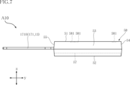
- the heights h of exposed portions 14B of lead 14, 15B of lead 15, and 16B of lead 16 are all the same (or approximately the same). Furthermore, their thicknesses are all the same (or approximately the same). Therefore, when viewed in the first direction x, at least a portion of lead 14 (exposed portion 14B) overlaps each of lead 15 and lead 16 (see FIG. 7).
- the plate-shaped conductive member 31 is bonded to the main surface electrode 211 of the semiconductor chip 21 and the die pad 10B. As a result, the main surface electrode 211 is electrically connected to the die pad 10B and the back surface electrode 223 of the semiconductor chip 22.
- the composition of the plate-shaped conductive member 31 includes copper.
- the composition of the plate-shaped conductive member 31 may include metals other than copper.
- the plate-shaped conductive member 31 is a metal clip.
- the plate-shaped conductive member 31 is formed by subjecting a metal plate of uniform thickness to cutting, bending, and the like.
- the plate-shaped conductive member 31 includes a suspension portion 311, two joint portions 312, 313, and a canopy portion 314.
- the suspension portion 311 forms a main part of the plate-shaped conductive member 31. As shown in FIG. 3, the suspension portion 311 is connected to each of the two joint portions 312, 313 and connects them. The suspension portion 311 extends in the first direction x. In the illustrated example, the suspension portion 311 extends linearly between the two semiconductor chips 21, 22 in a plan view. As shown in FIGS. 4 and 9, the suspension portion 311 straddles between the two die pads 10A, 10B. In the illustrated example, the end of the suspension portion 311 connected to the joint portion 312 is bifurcated. As shown in FIG. 4, the suspension portion 311 intersects one of a pair of edges 219b of the semiconductor chip 21 (the edge 219b closer to the semiconductor chip 22) in a plan view.
- the joint 312 is joined to the main surface electrode 211 of the semiconductor chip 21.
- the joint 312 includes two strip portions 312a.
- the two strip portions 312a are separated from each other in the second direction y.
- Each of the two strip portions 312a has the first direction x as its longitudinal direction.
- the two strip portions 312a are arranged parallel to each other in a planar view.
- the end portion connected to the joint 312 of the suspension portion 311 described above is bifurcated and each is connected to a corresponding one of the two strip portions 312a.
- the end of the suspension portion 311 connected to the joint portion 312 may not be bifurcated, and the joint portion 312 may be a single rectangular portion (a configuration in which two strip portions 312a are connected).
- the area of the joint portion 312 in a plan view (the total area of the two strip portions 312a) is, for example, 10% to 100% of the area of the main surface electrode 211 in a plan view.
- the joint 313 is joined to the seat surface 103 of the die pad 10B. As shown in Figure 3, the joint 313 extends in the second direction y. As shown in Figure 12, at least a portion of the joint 313 is contained in an area defined by the seat surface 103 and the upright surface 104 of the die pad 10B. The joint 313 is connected to the suspension portion 311. The joint 313 is located on the opposite side to the joint 312 with the suspension portion 311 in between.
- the semiconductor device A10 further includes a bonding layer 33.
- the bonding layer 33 is interposed between the main surface electrode 211 of the semiconductor chip 21 and the two strip portions 312a of the bonding portion 312.
- the bonding layer 33 bonds the main surface electrode 211 and the bonding portion 312 (the two strip portions 312a).
- the bonding layer 33 is conductive.
- the bonding layer 33 is, for example, solder. Alternatively, the bonding layer 33 may be a sintered metal.
- the thickness t31a (see FIG. 9) of the bonding portion 312 is not limited in any way, but is, for example, 0.1 mm or more and not more than twice the maximum thickness T1max (see FIG. 10) of the bonding layer 33.
- the maximum thickness T1max of the bonding layer 33 is greater than the thickness of the semiconductor chip 21.
- the semiconductor device A10 further includes a bonding layer 34.
- the bonding layer 34 is interposed between the seat surface 103 of the die pad 10B and the bonding portion 313.
- the bonding layer 34 bonds the die pad 10B and the bonding portion 313.
- the bonding layer 34 is conductive.
- the bonding layer 34 is, for example, solder.
- the bonding layer 34 may be a sintered metal.
- the eaves portion 314 is a different portion from the suspension portion 311 and is spaced apart from the suspension portion 311.
- the eaves portion 314 is not in contact with the bonding layer 33.
- the eaves portion 314 overlaps the outer periphery 219 of the semiconductor chip 21 in a planar view.
- the eaves portion 314 extends from the bonding portion 312.
- the eaves portion 314 protrudes from the principal surface electrode 211 in a planar view.
- the eaves portion 314 includes a pair of main body portions 314a and a pair of connecting portions 314b.
- Each of the pair of body portions 314a overlaps the outer periphery 219 of the semiconductor chip 21, as shown in FIG. 4.
- the pair of body portions 314a are spaced apart in the second direction y.
- the pair of body portions 314a are arranged on opposite sides of the joint portion 312 in the second direction y.
- Each of the pair of body portions 314a is strip-shaped extending in the first direction x.
- the pair of body portions 314a overlaps the pair of edges 219a individually in a planar view.
- the pair of body portions 314a overlaps the entire pair of edges 219a in a planar view, as shown in FIG. 4. Therefore, the pair of body portions 314a overlap the four corners of the semiconductor chip 21 in a planar view.
- Each body portion 314a does not contact any of the multiple principal surface electrodes 211, 212, 214.
- each body portion 314a is spaced apart from the main surface 21a, and as shown in FIG. 14, a sealing resin 50 is interposed between each body portion 314a and the main surface 21a in the thickness direction z.
- the pair of connecting portions 314b individually connect the joint portion 312 and the pair of main body portions 314a.
- Each of the pair of connecting portions 314b extends from the joint portion 312 in the second direction y.
- one of the pair of connecting portions 314b is connected to the one of the two band-shaped portions 312a that is located closest to one side of the second direction y
- the other of the pair of connecting portions 314b is connected to the one of the two band-shaped portions 312a that is located closest to the other side of the second direction y.
- the dimension of the pair of connecting portions 314b along the first direction x is smaller than the dimension of the pair of main body portions 314a along the first direction x.
- the multiple principal surface electrodes 212, 214 are exposed from the plate-shaped conductive member 31.
- Each connecting portion 314b is spaced apart from the main surface 21a, and as shown in FIG. 14, a sealing resin 50 is interposed between each connecting portion 314b and each main surface 21a in the thickness direction z.
- the thickness t31c (see FIG. 14) of the eaves portion 314 (each of the pair of main body portions 314a and each of the pair of connecting portions 314b) and the thickness t31b (see FIG. 9 and FIG. 10) of the joint portion 312 are the same (or approximately the same). Furthermore, the thickness t31c of the eaves portion 314 and the thickness t31a (see FIG. 9) of the suspension portion 311 are the same (or approximately the same). In this disclosure, the thickness t31c of the eaves portion 314 is the plate thickness at the eaves portion 314 and is the dimension along the vertical direction of the eaves portion 314 (corresponding to the thickness direction z in the illustrated example).
- the thickness t31b of the joint portion 312 is the plate thickness at the joint portion 312 and is the dimension along the vertical direction of the joint portion 312 (corresponding to the thickness direction z in the illustrated example).
- the thickness t31a of the suspension part 311 is the plate thickness of the suspension part 311, and is the dimension along the vertical direction of the suspension part 311.
- the suspension portion 321 forms the main portion of the plate-shaped conductive member 32. As shown in Figures 3 and 4, the suspension portion 321 is connected to each of the two joint portions 322, 323 and connects them. When viewed in the thickness direction z, the suspension portion 321 is bent in a hook shape. When viewed in the thickness direction z, the suspension portion 321 overlaps the main surface 101 of the die pad 10B. As shown in Figure 4, when viewed in a plan view, the suspension portion 321 intersects one of a pair of edges 229b of the semiconductor chip 22 (the edge 229b closer to the semiconductor chip 21).
- the overhanging portion 324 is a different portion from the suspension portion 321 and is spaced apart from the suspension portion 321.
- the overhanging portion 324 is not in contact with the bonding layer 35.
- the overhanging portion 324 overlaps the outer periphery 229 of the semiconductor chip 22 in a planar view.
- the overhanging portion 324 extends from the bonding portion 322.
- the overhanging portion 324 protrudes from the principal surface electrode 221 in a planar view.
- the overhanging portion 324 includes a pair of main body portions 324a and a pair of connecting portions 324b, as shown in Figures 4, 17, and 18.
- each of the pair of body portions 324a overlaps the outer periphery 229 of the semiconductor chip 22.
- the pair of body portions 324a are spaced apart in the second direction y.
- the pair of body portions 324a are arranged on opposite sides of the joint portion 322 in the second direction y.
- Each of the pair of body portions 324a is strip-shaped extending in the first direction x.
- the pair of body portions 324a overlap the pair of edges 229a individually in a planar view.
- the pair of body portions 324a overlap the entire pair of edges 229a in a planar view. Therefore, the pair of body portions 324a overlap the four corners of the semiconductor chip 22 in a planar view.
- Each body portion 324a does not contact any of the multiple principal surface electrodes 221, 222, 224.
- each body portion 324a is spaced apart from the main surface 22a, and as shown in FIG. 18, a sealing resin 50 is interposed between each body portion 324a and the main surface 22a in the thickness direction z.
- the dimension of the pair of connecting portions 324b along the first direction x is smaller than the dimension of the pair of main body portions 324a along the first direction x.
- the multiple principal surface electrodes 222, 224 are exposed from the plate-shaped conductive member 32.
- Each connecting portion 324b is spaced apart from the main surface 22a, and as shown in FIG. 18, a sealing resin 50 is interposed between each connecting portion 324b and each main surface 22a in the thickness direction z.
- Each of the multiple connection members 41A, 41B, 42A, and 42B is, for example, a bonding wire.
- the composition of each of the multiple connection members 41A, 41B, 42A, and 42B includes gold.
- the composition of each of the multiple connection members 41A, 41B, 42A, and 42B may include copper or aluminum (Al).
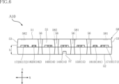
- the semiconductor device A10 As shown in FIG. 19, in the semiconductor device A10 configured as described above, the main surface electrode 211 of the semiconductor chip 21 and the back surface electrode 223 of the semiconductor chip 22 are electrically connected. Therefore, the semiconductor device A10 forms a half-bridge circuit using two transistors (two semiconductor chips 21 and 22).
- the principal surface electrodes 221 of the semiconductor chip 22 and the leads 14 (conductive objects) are electrically connected via the plate-shaped conductive member 32.
- the wiring resistance between the principal surface electrodes 221 and the leads 14 (conductive objects) can be reduced compared to a configuration in which the principal surface electrodes 221 and the leads 14 (conductive objects) are connected by bonding wires. Therefore, the semiconductor device A10 can reduce power loss.
- the plate-shaped conductive member 32 includes a visor portion 324 different from the suspension portion 321, and the visor portion 324 is not in contact with the bonding layer 33 and overlaps the outer periphery 229 of the semiconductor chip 22 when viewed in the thickness direction z.
- the semiconductor chip 22 When the semiconductor chip 22 is energized, the semiconductor chip 22 generates heat. This heat generates thermal stress on the semiconductor chip 22.
- the plate-shaped conductive member 32 metal plate
- the thermal stress applied to the semiconductor chip 22 is larger than when a bonding wire is used.
- the main surface electrode 211 (anode electrode) of the semiconductor chip 21 and the back surface electrode 223 (drain electrode) of the semiconductor chip 22 are electrically connected.
- the high voltage side is a diode and the low voltage side is a transistor.
- the semiconductor device A11 is used, for example, as a boost chopper circuit.
- the semiconductor device A12 does not include any of the multiple connection members 41B, 42A, 42B.
- each lead 172, 181, 182 is not electrically connected to either of the two semiconductor chips 21, 22. Therefore, in the semiconductor device A12, each lead 172, 181, 182 is a non-connect terminal.
- the semiconductor device A12 does not include any of the pair of connection members 42A, 42B, but in a configuration different from this example, the semiconductor device A12 may include a pair of connection members 42A, 42B similar to the semiconductor device A10.
- the main surface electrode 211 (source electrode) of the semiconductor chip 21 and the back surface electrode 223 (cathode electrode) of the semiconductor chip 22 are electrically connected.
- the high voltage side becomes a transistor and the low voltage side becomes a diode.
- the semiconductor device A12 is used, for example, as a step-down chopper circuit.
- Semiconductor chip 21 of semiconductor device A13 is a diode, similar to semiconductor chip 21 of semiconductor device A11. Also, semiconductor chip 22 of semiconductor device A13 is a diode, similar to semiconductor chip 22 of semiconductor device A12.
- the main surface electrode 211 (anode electrode) of the semiconductor chip 21 and the back surface electrode 223 (cathode electrode) of the semiconductor chip 22 are electrically connected.
- both the high voltage side and the low voltage side are diodes with respect to the power supply voltage (DC voltage) applied between the two leads 14, 15.
- the semiconductor device A13 is a diode bridge circuit.
- each of the semiconductor devices A11 to A13 can reduce the mounting area on the circuit board on which the semiconductor devices A11 to A13 are mounted.
- each of the semiconductor devices A11 to A13 has a common configuration with the semiconductor device A10, and thus achieves the same effects as the semiconductor device A10.
- each main body portion 314a is located above the joint portion 312 in the thickness direction z. Therefore, as shown in Figure 27, the end of each connecting portion 314b that is connected to the main body portion 314a is bent upward in the thickness direction z.
- the amount of deviation ⁇ z1 (see Figure 27) in the thickness direction z between each main body portion 314a and the joint portion 312 (each band-shaped portion 312a) is 20% or more and 300% or less of the thickness t31a of the suspension portion 311. In one example, the amount of deviation ⁇ z1 is 50 ⁇ m or more and 500 ⁇ m or less.
- the misalignment amount ⁇ z1 is set to a positive value when the underside (the surface facing downward in the thickness direction z) of each main body portion 314a is located above in the thickness direction z, and is set to a negative value when the underside of each main body portion 314a is located below in the thickness direction z, based on the underside (the surface facing downward in the thickness direction z) of the joint portion 312 (each band portion 312a).
- the misalignment amount ⁇ z1 is 0.
- the amount of deviation ⁇ z2 is set to a positive value when the underside (the surface facing downward in the thickness direction z) of each main body portion 324a is located above in the thickness direction z, based on the underside (the surface facing downward in the thickness direction z) of the joint portion 322 (each band-shaped portion 322a) and is set to a negative value when the underside of each main body portion 324a is located below in the thickness direction z.
- the amount of deviation ⁇ z2 is 0.
- the semiconductor device A20 can reduce the wiring resistance between the main surface electrode 221 and the lead 14 (conductive object for the main surface electrode 221) by the plate-shaped conductive member 32, and therefore can reduce power loss. Also, like the semiconductor device A10, the semiconductor device A20 can reduce the wiring resistance between the main surface electrode 211 and the die pad 10B (conductive object for the main surface electrode 211) by the plate-shaped conductive member 31, and therefore can reduce power loss. Also, like the semiconductor device A10, the semiconductor device A20 can reduce the thermal stress applied to the semiconductor chip 22 by the eaves portion 324 of the plate-shaped conductive member 32.
- the semiconductor device A20 can reduce the thermal stress applied to the semiconductor chip 21 by the eaves portion 314 of the plate-shaped conductive member 31.
- the semiconductor device A20 has the same configuration as the semiconductor device A10, and therefore has the same effects.
- each main body 324a and the joint 322 in the thickness direction z is greater than 20% and less than 300% of the thickness t32a of the suspension portion 321.
- the thermal stress applied to the semiconductor chip 22 is alleviated more than when the shift amount ⁇ z2 deviates from the upper limit of this range. That is, a configuration in which the deviation amount ⁇ z2 is within the above-mentioned range is preferable in terms of alleviating the thermal stress of the semiconductor chip 22. This is also true for the eaves portion 314 of the plate-shaped conductive member 31.
- the semiconductor device A20 can further alleviate the thermal stress applied to the semiconductor chip 21 than the semiconductor device A10.
- the deviation amount ⁇ z1 in the thickness direction z between each main body portion 314a and the joint portion 312 is greater than 20% and less than 300% of the thickness t31a of the suspension portion 311.
- the thermal stress applied to the semiconductor chip 21 is alleviated more than when the deviation amount ⁇ z1 deviates from the upper limit of this range. That is, a configuration in which the deviation amount ⁇ z1 is within the above-mentioned range is preferable in terms of alleviating the thermal stress of the semiconductor chip 21.
- FIG. 29 shows a semiconductor device A21 according to a modified example of the second embodiment.
- the semiconductor device A21 differs from the semiconductor device A20 in the following respects.
- each main body portion 314a is located below the bonding portion 312 in the thickness direction z. Therefore, as shown in FIG. 29, the end of each connecting portion 324b that is connected to the main body portion 324a is bent downward in the thickness direction z.
- the aforementioned deviation amount ⁇ z1 (see FIG. 29) is equal to or greater than the negative value (-T1max) of the maximum thickness T1max of the bonding layer 33 and less than 0 (zero).
- the deviation amount ⁇ z1 is the negative value (-T1max) of the maximum thickness T1max of the bonding layer 33
- each main body portion 314a contacts the main surface 21a. Note that FIG. 29 shows a case where each main body portion 314a is separated from the main surface 21a in the thickness direction z.
- each body portion 324a and the joint portion 322 is the same (or approximately the same) as the positional relationship between each body portion 314a and the joint portion 312.
- each body portion 324a is located below the joint portion 322 in the thickness direction z. Therefore, the end portion of each connecting portion 324b that is connected to the body portion 324a is bent downward in the thickness direction z.
- the aforementioned deviation amount ⁇ z2 is equal to or greater than the negative value (-T2max) of the maximum thickness T2max of the joint layer 34 and less than 0 (zero).
- the deviation amount ⁇ z2 is the negative value (-T2max) of the maximum thickness T2max of the joint layer 34
- each body portion 324a contacts the main surface 22a.
- semiconductor device A21 can reduce power loss through plate-shaped conductive member 32, reduce power loss through plate-shaped conductive member 31, alleviate thermal stress through eaves portion 324 of plate-shaped conductive member 32, and alleviate thermal stress through eaves portion 314 of plate-shaped conductive member 31.
- each main body portion 314a and the joint portion 312 may be shifted upward in the thickness direction z, may be shifted downward in the thickness direction z, or may not be shifted.
- the semiconductor device of the present disclosure is not limited in any way as to whether each main body portion 314a is shifted with respect to the joint portion 312, or whether it is shifted upward or downward in the thickness direction z.
- each main body portion 314a is shifted upward in the thickness direction z with respect to the joint portion 312 is preferable.
- each main body portion 324a and the joint portion 322 may be shifted upward in the thickness direction z, may be shifted downward in the thickness direction z, or may not be shifted.
- each main body portion 324a is misaligned with respect to the joint portion 322, or whether it is misaligned upward or downward in the thickness direction z.
- a configuration in which each main body portion 324a is misaligned upward in the thickness direction z with respect to the joint portion 322 is preferable.
- Third embodiment show a semiconductor device A30 according to the third embodiment.
- the semiconductor device A30 is different from the semiconductor device A10 in the following respects.
- the overhanging portion 314 of the semiconductor device A30 is thicker than the suspension portion 311.
- the overhanging portion 324 of the semiconductor device A30 is thicker than the suspension portion 321.
- the thickness t31b of the joint 312 is greater than the thickness t31a of the suspension portion 311.
- the thickness t31b of the joint 312 and the thickness t31c of the eaves portion 314 are the same (or approximately the same). Therefore, the thickness t31c of the eaves portion 314 is greater than the thickness t31a of the suspension portion 311.
- the thickness t31c of the eaves portion 314 is greater than 100% and less than 300% of the thickness of the suspension portion 311.
- the thickness t31c of the eaves portion 314 is greater than 50% and less than 300% of the maximum thickness T1max of the joint layer 33.
- the thickness t31c of the eaves portion 314 is greater than 125 ⁇ m and less than 500 ⁇ m.
- the suspension portion 311 is connected to the lower end of the joint portion 312 (each band portion 312a) in the thickness direction z, but in a different example, it may be connected to the upper end of the joint portion 312 (each band portion 312a) in the thickness direction z.
- the thickness t32b of the joint 322 is greater than the thickness t32a of the suspension portion 321.
- the thickness t32b of the joint 322 and the thickness t32c of the eaves portion 324 are the same (or approximately the same). Therefore, the thickness t32c of the eaves portion 324 is greater than the thickness t32a of the suspension portion 321.
- the thickness t32c of the eaves portion 324 is greater than 100% and less than 300% of the thickness t32a of the suspension portion 321.
- the thickness t32c of the eaves portion 324 is greater than 50% and less than 300% of the maximum thickness T2max of the joint layer 35.
- the thickness t32c of the eaves portion 324 is greater than 125 ⁇ m and less than 500 ⁇ m.
- the suspension portion 321 is connected to the lower end of the joint portion 322 (each band portion 322a) in the thickness direction z, but in a different example, it may be connected to the upper end of the joint portion 322 (each band portion 322a) in the thickness direction z.
- the semiconductor device A30 can reduce the wiring resistance between the main surface electrode 221 and the lead 14 (conductive object for the main surface electrode 221) by the plate-shaped conductive member 32, and therefore can reduce power loss. Also, like the semiconductor device A10, the semiconductor device A30 can reduce the wiring resistance between the main surface electrode 211 and the die pad 10B (conductive object for the main surface electrode 211) by the plate-shaped conductive member 31, and therefore can reduce power loss. Also, like the semiconductor device A10, the semiconductor device A30 can reduce the thermal stress applied to the semiconductor chip 22 by the eaves portion 324 of the plate-shaped conductive member 32.
- the eaves portion 324 of the plate-shaped conductive member 32 is thicker than the suspension portion 321.
- the thickness t32c of the eaves portion 324 is greater than 100% and less than 300% of the thickness t32a of the suspension portion 321. Even if the eaves portion 324 is thicker than the suspension portion 321, the thermal stress applied to the semiconductor chip 22 can be alleviated.
- the joint portion 322 also becomes thicker, so it is necessary to increase the pressing force when joining the plate-shaped conductive member 32 to the main surface electrode 221. This may cause damage to the main surface electrode 221.
- the semiconductor device A30 can alleviate the thermal stress applied to the semiconductor chip 22 and suppress damage to the main surface electrode 221.
- the thickness t32c of the eaves portion 324 may be set to 50% to 300% of the maximum thickness T2max of the bonding layer 35 instead of the thickness t32a of the suspension portion 321. In this case, the thermal stress applied to the semiconductor chip 22 can be reduced and the damage to the main surface electrode 221 can be suppressed.
- the thickness t31c of the eaves portion 314 of the plate-shaped conductive member 31 can be set to be greater than 100% and less than 300% of the thickness t31a of the suspension portion 311, and the thermal stress applied to the semiconductor chip 21 can be reduced and the damage to the main surface electrode 211 can be suppressed.
- the thickness t31c of the eaves portion 314 of the plate-shaped conductive member 31 can be set to be greater than 100% and less than 300% of the thickness t31a of the suspension portion 311, and the thermal stress applied to the semiconductor chip 21 can be reduced and the damage to the main surface electrode 211 can be suppressed.
- the thickness t31c of the eaves portion 314 may be set to 50% to 300% of the maximum thickness T1max of the bonding layer 33 instead of the thickness t31a of the suspension portion 311. In this case, the thermal stress applied to the semiconductor chip 21 can be similarly alleviated and damage to the main surface electrode 211 can be suppressed.
- the eaves portion 314 may be thinner than the suspension portion 311.
- the thickness t31c of the plate-shaped conductive member 31 is 50% or more and less than 100% of the thickness t31a of the suspension portion 311. Even if the eaves portion 314 is thinner than the suspension portion 311, the thermal stress applied to the semiconductor chip 21 can be alleviated. On the other hand, if the eaves portion 314 is thinner than the suspension portion 311, the joint portion 312 will also be thinner, and the wiring resistance at the joint portion 312 will be large.
- the thickness t32c of the eaves portion 324 may be larger, smaller, or the same as the thickness t32a of the suspension portion 321.
- the plate-shaped conductive member 32 includes the overhanging portion 324, there is no limitation on the relative thickness relationship between the overhanging portion 324 and the suspension portion 321.
- Fourth embodiment 33 shows a semiconductor device A40 according to the fourth embodiment.
- the semiconductor device A40 is different from the semiconductor device A10 in the following respects. First, the region of the overhanging portion 314 of the semiconductor device A40 that overlaps with the outer periphery 219 is different. Second, the region of the overhanging portion 314 of the semiconductor device A40 that overlaps with the outer periphery 229 is different.
- the eaves portion 314 (each main body portion 314a and each connecting portion 314b) of the semiconductor device A40 does not overlap the entirety of each edge 219a of the outer periphery 219, but overlaps a portion of each edge 219a. In this embodiment, the eaves portion 314 does not overlap any of the four corners of the semiconductor chip 21 in a planar view.
- the dimension along the first direction x of each main body portion 314a and the dimension along the first direction x of each connecting portion 314b are the same (or approximately the same), but the dimension along the first direction x of each main body portion 314a may be larger or smaller than the dimension along the first direction x of each connecting portion 314b.
- the configuration of the eaves portion 314 is the same for the eaves portion 324.
- the eaves portion 324 (each main body portion 324a and each connecting portion 324b) of the semiconductor device A40 does not overlap the entirety of each edge 229a of the outer periphery 229, but overlaps a portion of each edge 229a.
- the semiconductor device A40 can reduce the wiring resistance between the main surface electrode 221 and the lead 14 (conductive object for the main surface electrode 221) by the plate-shaped conductive member 32, and therefore can reduce power loss. Also, like the semiconductor device A10, the semiconductor device A40 can reduce the wiring resistance between the main surface electrode 211 and the die pad 10B (conductive object for the main surface electrode 211) by the plate-shaped conductive member 31, and therefore can reduce power loss. Also, like the semiconductor device A10, the semiconductor device A40 can reduce the thermal stress applied to the semiconductor chip 22 by the eaves portion 324 of the plate-shaped conductive member 32.
- the semiconductor device A40 can reduce the thermal stress applied to the semiconductor chip 21 by the eaves portion 314 of the plate-shaped conductive member 31.
- the semiconductor device A40 has the same configuration as the semiconductor device A10, and therefore has the same effects.
- each of the semiconductor devices A41 and A42 similar to the semiconductor device A40, it is possible to reduce power loss by the plate-shaped conductive member 32, reduce power loss by the plate-shaped conductive member 31, alleviate thermal stress by the eaves portion 324 of the plate-shaped conductive member 32, and alleviate thermal stress by the eaves portion 314 of the plate-shaped conductive member 31.
- the semiconductor device A50 can reduce the wiring resistance between the main surface electrode 221 and the lead 14 (conductive object for the main surface electrode 221) by the plate-shaped conductive member 32, and therefore can reduce power loss. Also, like the semiconductor device A10, the semiconductor device A50 can reduce the wiring resistance between the main surface electrode 211 and the die pad 10B (conductive object for the main surface electrode 211) by the plate-shaped conductive member 31, and therefore can reduce power loss. Also, like the semiconductor device A10, the semiconductor device A50 can reduce the thermal stress applied to the semiconductor chip 22 by the eaves portion 324 of the plate-shaped conductive member 32.
- the semiconductor device A50 can reduce the thermal stress applied to the semiconductor chip 21 by the eaves portion 314 of the plate-shaped conductive member 31.
- the semiconductor device A50 has the same configuration as the semiconductor device A10, and therefore has the same effects.
- the eaves portion 314 of the plate-shaped conductive member 31 includes a pair of body portions 314a, but the eaves portion 314 may include only one of the pair of body portions 314a. In this case, the eaves portion 314 may not include the connecting portion 314b corresponding to one of the pair of body portions 314a.
- the package structure of the semiconductor device disclosed herein is not limited to a specific configuration and may be, for example, SOP (Small Outline Package), QFP (Quad Flat Package), BGA (Ball grid array), LGA (Land grid array), DFN (Dual Flatpack No-leaded), QFN (Quad Flatpack No-leaded), etc.
Landscapes
- Structures Or Materials For Encapsulating Or Coating Semiconductor Devices Or Solid State Devices (AREA)
Priority Applications (1)
| Application Number | Priority Date | Filing Date | Title |
|---|---|---|---|
| JP2024568715A JPWO2024147269A1 (https=) | 2023-01-06 | 2023-12-14 |
Applications Claiming Priority (2)
| Application Number | Priority Date | Filing Date | Title |
|---|---|---|---|
| JP2023-001097 | 2023-01-06 | ||
| JP2023001097 | 2023-01-06 |
Publications (1)
| Publication Number | Publication Date |
|---|---|
| WO2024147269A1 true WO2024147269A1 (ja) | 2024-07-11 |
Family
ID=91803899
Family Applications (1)
| Application Number | Title | Priority Date | Filing Date |
|---|---|---|---|
| PCT/JP2023/044791 Ceased WO2024147269A1 (ja) | 2023-01-06 | 2023-12-14 | 半導体装置 |
Country Status (2)
| Country | Link |
|---|---|
| JP (1) | JPWO2024147269A1 (https=) |
| WO (1) | WO2024147269A1 (https=) |
Citations (3)
| Publication number | Priority date | Publication date | Assignee | Title |
|---|---|---|---|---|
| US20150115313A1 (en) * | 2013-10-31 | 2015-04-30 | Infineon Technologies Austria Ag | Semiconductor Device Package |
| WO2016084180A1 (ja) * | 2014-11-27 | 2016-06-02 | 三菱電機株式会社 | 半導体モジュールおよび半導体駆動装置 |
| JP2019079935A (ja) * | 2017-10-25 | 2019-05-23 | 三菱電機株式会社 | 電力用半導体装置 |
-
2023
- 2023-12-14 WO PCT/JP2023/044791 patent/WO2024147269A1/ja not_active Ceased
- 2023-12-14 JP JP2024568715A patent/JPWO2024147269A1/ja active Pending
Patent Citations (3)
| Publication number | Priority date | Publication date | Assignee | Title |
|---|---|---|---|---|
| US20150115313A1 (en) * | 2013-10-31 | 2015-04-30 | Infineon Technologies Austria Ag | Semiconductor Device Package |
| WO2016084180A1 (ja) * | 2014-11-27 | 2016-06-02 | 三菱電機株式会社 | 半導体モジュールおよび半導体駆動装置 |
| JP2019079935A (ja) * | 2017-10-25 | 2019-05-23 | 三菱電機株式会社 | 電力用半導体装置 |
Also Published As
| Publication number | Publication date |
|---|---|
| JPWO2024147269A1 (https=) | 2024-07-11 |
Similar Documents
| Publication | Publication Date | Title |
|---|---|---|
| CN103811452B (zh) | 半导体器件及其制造方法 | |
| EP3813106B1 (en) | Semiconductor device | |
| US9054040B2 (en) | Multi-die package with separate inter-die interconnects | |
| US20120064667A1 (en) | Semiconductor die package including multiple dies and a common node structure | |
| US20150069590A1 (en) | Multi-Die Power Semiconductor Device Packaged On a Lead Frame Unit with Multiple Carrier Pins and a Metal Clip | |
| US9711481B2 (en) | Semiconductor device and semiconductor device mounting structure | |
| US20100181628A1 (en) | Semiconductor device | |
| US20120248593A1 (en) | Package structure for dc-dc converter | |
| CN103972277B (zh) | 半导体装置及其制造方法 | |
| US11996344B2 (en) | Semiconductor device | |
| US20260005108A1 (en) | Semiconductor power module package having lead frame anchored bars | |
| KR101644913B1 (ko) | 초음파 용접을 이용한 반도체 패키지 및 제조 방법 | |
| WO2011039795A1 (ja) | 半導体装置とその製造方法 | |
| WO2024147269A1 (ja) | 半導体装置 | |
| WO2024080089A1 (ja) | 半導体装置および半導体装置の製造方法 | |
| WO2025158868A1 (ja) | 半導体装置 | |
| WO2023243343A1 (ja) | 半導体装置 | |
| WO2024004614A1 (ja) | 半導体装置 | |
| US20240282690A1 (en) | Semiconductor device | |
| US20250357284A1 (en) | Electronic devices and methods of manufacturing electronic devices | |
| US20240282681A1 (en) | Semiconductor device, and semiconductor device mounting body | |
| US20250391804A1 (en) | Semiconductor device and electronic device | |
| US12327780B2 (en) | Semiconductor device including a lead and a sealing resin | |
| US20240047315A1 (en) | Semiconductor device | |
| WO2024029249A1 (ja) | 半導体装置 |
Legal Events
| Date | Code | Title | Description |
|---|---|---|---|
| 121 | Ep: the epo has been informed by wipo that ep was designated in this application |
Ref document number: 23914757 Country of ref document: EP Kind code of ref document: A1 |
|
| WWE | Wipo information: entry into national phase |
Ref document number: 2024568715 Country of ref document: JP |
|
| NENP | Non-entry into the national phase |
Ref country code: DE |
|
| 122 | Ep: pct application non-entry in european phase |
Ref document number: 23914757 Country of ref document: EP Kind code of ref document: A1 |