WO2024143377A1 - 半導体装置 - Google Patents
半導体装置 Download PDFInfo
- Publication number
- WO2024143377A1 WO2024143377A1 PCT/JP2023/046698 JP2023046698W WO2024143377A1 WO 2024143377 A1 WO2024143377 A1 WO 2024143377A1 JP 2023046698 W JP2023046698 W JP 2023046698W WO 2024143377 A1 WO2024143377 A1 WO 2024143377A1
- Authority
- WO
- WIPO (PCT)
- Prior art keywords
- layer
- region
- regions
- less
- thickness
- Prior art date
- Legal status (The legal status is an assumption and is not a legal conclusion. Google has not performed a legal analysis and makes no representation as to the accuracy of the status listed.)
- Ceased
Links
Images






























Classifications
-
- H—ELECTRICITY
- H10—SEMICONDUCTOR DEVICES; ELECTRIC SOLID-STATE DEVICES NOT OTHERWISE PROVIDED FOR
- H10W—GENERIC PACKAGES, INTERCONNECTIONS, CONNECTORS OR OTHER CONSTRUCTIONAL DETAILS OF DEVICES COVERED BY CLASS H10
- H10W46/00—Marks applied to devices, e.g. for alignment or identification
-
- H—ELECTRICITY
- H10—SEMICONDUCTOR DEVICES; ELECTRIC SOLID-STATE DEVICES NOT OTHERWISE PROVIDED FOR
- H10D—INORGANIC ELECTRIC SEMICONDUCTOR DEVICES
- H10D30/00—Field-effect transistors [FET]
- H10D30/01—Manufacture or treatment
- H10D30/021—Manufacture or treatment of FETs having insulated gates [IGFET]
- H10D30/028—Manufacture or treatment of FETs having insulated gates [IGFET] of double-diffused metal oxide semiconductor [DMOS] FETs
- H10D30/0291—Manufacture or treatment of FETs having insulated gates [IGFET] of double-diffused metal oxide semiconductor [DMOS] FETs of vertical DMOS [VDMOS] FETs
-
- H—ELECTRICITY
- H10—SEMICONDUCTOR DEVICES; ELECTRIC SOLID-STATE DEVICES NOT OTHERWISE PROVIDED FOR
- H10D—INORGANIC ELECTRIC SEMICONDUCTOR DEVICES
- H10D12/00—Bipolar devices controlled by the field effect, e.g. insulated-gate bipolar transistors [IGBT]
-
- H—ELECTRICITY
- H10—SEMICONDUCTOR DEVICES; ELECTRIC SOLID-STATE DEVICES NOT OTHERWISE PROVIDED FOR
- H10D—INORGANIC ELECTRIC SEMICONDUCTOR DEVICES
- H10D12/00—Bipolar devices controlled by the field effect, e.g. insulated-gate bipolar transistors [IGBT]
- H10D12/411—Insulated-gate bipolar transistors [IGBT]
-
- H—ELECTRICITY
- H10—SEMICONDUCTOR DEVICES; ELECTRIC SOLID-STATE DEVICES NOT OTHERWISE PROVIDED FOR
- H10D—INORGANIC ELECTRIC SEMICONDUCTOR DEVICES
- H10D12/00—Bipolar devices controlled by the field effect, e.g. insulated-gate bipolar transistors [IGBT]
- H10D12/411—Insulated-gate bipolar transistors [IGBT]
- H10D12/441—Vertical IGBTs
- H10D12/461—Vertical IGBTs having non-planar surfaces, e.g. having trenches, recesses or pillars in the surfaces of the emitter, base or collector regions
- H10D12/481—Vertical IGBTs having non-planar surfaces, e.g. having trenches, recesses or pillars in the surfaces of the emitter, base or collector regions having gate structures on slanted surfaces, on vertical surfaces, or in grooves, e.g. trench gate IGBTs
-
- H—ELECTRICITY
- H10—SEMICONDUCTOR DEVICES; ELECTRIC SOLID-STATE DEVICES NOT OTHERWISE PROVIDED FOR
- H10D—INORGANIC ELECTRIC SEMICONDUCTOR DEVICES
- H10D30/00—Field-effect transistors [FET]
- H10D30/01—Manufacture or treatment
- H10D30/021—Manufacture or treatment of FETs having insulated gates [IGFET]
- H10D30/028—Manufacture or treatment of FETs having insulated gates [IGFET] of double-diffused metal oxide semiconductor [DMOS] FETs
- H10D30/0291—Manufacture or treatment of FETs having insulated gates [IGFET] of double-diffused metal oxide semiconductor [DMOS] FETs of vertical DMOS [VDMOS] FETs
- H10D30/0297—Manufacture or treatment of FETs having insulated gates [IGFET] of double-diffused metal oxide semiconductor [DMOS] FETs of vertical DMOS [VDMOS] FETs using recessing of the gate electrodes, e.g. to form trench gate electrodes
-
- H—ELECTRICITY
- H10—SEMICONDUCTOR DEVICES; ELECTRIC SOLID-STATE DEVICES NOT OTHERWISE PROVIDED FOR
- H10D—INORGANIC ELECTRIC SEMICONDUCTOR DEVICES
- H10D30/00—Field-effect transistors [FET]
- H10D30/60—Insulated-gate field-effect transistors [IGFET]
- H10D30/64—Double-diffused metal-oxide semiconductor [DMOS] FETs
- H10D30/66—Vertical DMOS [VDMOS] FETs
-
- H—ELECTRICITY
- H10—SEMICONDUCTOR DEVICES; ELECTRIC SOLID-STATE DEVICES NOT OTHERWISE PROVIDED FOR
- H10D—INORGANIC ELECTRIC SEMICONDUCTOR DEVICES
- H10D30/00—Field-effect transistors [FET]
- H10D30/60—Insulated-gate field-effect transistors [IGFET]
- H10D30/64—Double-diffused metal-oxide semiconductor [DMOS] FETs
- H10D30/66—Vertical DMOS [VDMOS] FETs
- H10D30/665—Vertical DMOS [VDMOS] FETs having edge termination structures
-
- H—ELECTRICITY
- H10—SEMICONDUCTOR DEVICES; ELECTRIC SOLID-STATE DEVICES NOT OTHERWISE PROVIDED FOR
- H10D—INORGANIC ELECTRIC SEMICONDUCTOR DEVICES
- H10D30/00—Field-effect transistors [FET]
- H10D30/60—Insulated-gate field-effect transistors [IGFET]
- H10D30/64—Double-diffused metal-oxide semiconductor [DMOS] FETs
- H10D30/66—Vertical DMOS [VDMOS] FETs
- H10D30/668—Vertical DMOS [VDMOS] FETs having trench gate electrodes, e.g. UMOS transistors
-
- H—ELECTRICITY
- H10—SEMICONDUCTOR DEVICES; ELECTRIC SOLID-STATE DEVICES NOT OTHERWISE PROVIDED FOR
- H10D—INORGANIC ELECTRIC SEMICONDUCTOR DEVICES
- H10D62/00—Semiconductor bodies, or regions thereof, of devices having potential barriers
- H10D62/01—Manufacture or treatment
- H10D62/051—Forming charge compensation regions, e.g. superjunctions
- H10D62/054—Forming charge compensation regions, e.g. superjunctions by high energy implantations in bulk semiconductor bodies, e.g. forming pillars
-
- H—ELECTRICITY
- H10—SEMICONDUCTOR DEVICES; ELECTRIC SOLID-STATE DEVICES NOT OTHERWISE PROVIDED FOR
- H10D—INORGANIC ELECTRIC SEMICONDUCTOR DEVICES
- H10D62/00—Semiconductor bodies, or regions thereof, of devices having potential barriers
- H10D62/10—Shapes, relative sizes or dispositions of the regions of the semiconductor bodies; Shapes of the semiconductor bodies
-
- H—ELECTRICITY
- H10—SEMICONDUCTOR DEVICES; ELECTRIC SOLID-STATE DEVICES NOT OTHERWISE PROVIDED FOR
- H10D—INORGANIC ELECTRIC SEMICONDUCTOR DEVICES
- H10D62/00—Semiconductor bodies, or regions thereof, of devices having potential barriers
- H10D62/10—Shapes, relative sizes or dispositions of the regions of the semiconductor bodies; Shapes of the semiconductor bodies
- H10D62/102—Constructional design considerations for preventing surface leakage or controlling electric field concentration
- H10D62/103—Constructional design considerations for preventing surface leakage or controlling electric field concentration for increasing or controlling the breakdown voltage of reverse-biased devices
- H10D62/105—Constructional design considerations for preventing surface leakage or controlling electric field concentration for increasing or controlling the breakdown voltage of reverse-biased devices by having particular doping profiles, shapes or arrangements of PN junctions; by having supplementary regions, e.g. junction termination extension [JTE]
- H10D62/106—Constructional design considerations for preventing surface leakage or controlling electric field concentration for increasing or controlling the breakdown voltage of reverse-biased devices by having particular doping profiles, shapes or arrangements of PN junctions; by having supplementary regions, e.g. junction termination extension [JTE] having supplementary regions doped oppositely to or in rectifying contact with regions of the semiconductor bodies, e.g. guard rings with PN or Schottky junctions
-
- H—ELECTRICITY
- H10—SEMICONDUCTOR DEVICES; ELECTRIC SOLID-STATE DEVICES NOT OTHERWISE PROVIDED FOR
- H10D—INORGANIC ELECTRIC SEMICONDUCTOR DEVICES
- H10D62/00—Semiconductor bodies, or regions thereof, of devices having potential barriers
- H10D62/10—Shapes, relative sizes or dispositions of the regions of the semiconductor bodies; Shapes of the semiconductor bodies
- H10D62/102—Constructional design considerations for preventing surface leakage or controlling electric field concentration
- H10D62/103—Constructional design considerations for preventing surface leakage or controlling electric field concentration for increasing or controlling the breakdown voltage of reverse-biased devices
- H10D62/105—Constructional design considerations for preventing surface leakage or controlling electric field concentration for increasing or controlling the breakdown voltage of reverse-biased devices by having particular doping profiles, shapes or arrangements of PN junctions; by having supplementary regions, e.g. junction termination extension [JTE]
- H10D62/109—Reduced surface field [RESURF] PN junction structures
- H10D62/111—Multiple RESURF structures, e.g. double RESURF or 3D-RESURF structures
-
- H—ELECTRICITY
- H10—SEMICONDUCTOR DEVICES; ELECTRIC SOLID-STATE DEVICES NOT OTHERWISE PROVIDED FOR
- H10D—INORGANIC ELECTRIC SEMICONDUCTOR DEVICES
- H10D62/00—Semiconductor bodies, or regions thereof, of devices having potential barriers
- H10D62/10—Shapes, relative sizes or dispositions of the regions of the semiconductor bodies; Shapes of the semiconductor bodies
- H10D62/13—Semiconductor regions connected to electrodes carrying current to be rectified, amplified or switched, e.g. source or drain regions
- H10D62/149—Source or drain regions of field-effect devices
- H10D62/151—Source or drain regions of field-effect devices of IGFETs
- H10D62/156—Drain regions of DMOS transistors
- H10D62/157—Impurity concentrations or distributions
-
- H—ELECTRICITY
- H10—SEMICONDUCTOR DEVICES; ELECTRIC SOLID-STATE DEVICES NOT OTHERWISE PROVIDED FOR
- H10D—INORGANIC ELECTRIC SEMICONDUCTOR DEVICES
- H10D62/00—Semiconductor bodies, or regions thereof, of devices having potential barriers
- H10D62/10—Shapes, relative sizes or dispositions of the regions of the semiconductor bodies; Shapes of the semiconductor bodies
- H10D62/17—Semiconductor regions connected to electrodes not carrying current to be rectified, amplified or switched, e.g. channel regions
- H10D62/393—Body regions of DMOS transistors or IGBTs
-
- H—ELECTRICITY
- H10—SEMICONDUCTOR DEVICES; ELECTRIC SOLID-STATE DEVICES NOT OTHERWISE PROVIDED FOR
- H10D—INORGANIC ELECTRIC SEMICONDUCTOR DEVICES
- H10D62/00—Semiconductor bodies, or regions thereof, of devices having potential barriers
- H10D62/40—Crystalline structures
- H10D62/405—Orientations of crystalline planes
-
- H—ELECTRICITY
- H10—SEMICONDUCTOR DEVICES; ELECTRIC SOLID-STATE DEVICES NOT OTHERWISE PROVIDED FOR
- H10D—INORGANIC ELECTRIC SEMICONDUCTOR DEVICES
- H10D62/00—Semiconductor bodies, or regions thereof, of devices having potential barriers
- H10D62/80—Semiconductor bodies, or regions thereof, of devices having potential barriers characterised by the materials
- H10D62/81—Semiconductor bodies, or regions thereof, of devices having potential barriers characterised by the materials of structures exhibiting quantum-confinement effects, e.g. single quantum wells; of structures having periodic or quasi-periodic potential variation
-
- H—ELECTRICITY
- H10—SEMICONDUCTOR DEVICES; ELECTRIC SOLID-STATE DEVICES NOT OTHERWISE PROVIDED FOR
- H10D—INORGANIC ELECTRIC SEMICONDUCTOR DEVICES
- H10D62/00—Semiconductor bodies, or regions thereof, of devices having potential barriers
- H10D62/80—Semiconductor bodies, or regions thereof, of devices having potential barriers characterised by the materials
- H10D62/83—Semiconductor bodies, or regions thereof, of devices having potential barriers characterised by the materials being Group IV materials, e.g. B-doped Si or undoped Ge
- H10D62/832—Semiconductor bodies, or regions thereof, of devices having potential barriers characterised by the materials being Group IV materials, e.g. B-doped Si or undoped Ge being Group IV materials comprising two or more elements, e.g. SiGe
- H10D62/8325—Silicon carbide
-
- H—ELECTRICITY
- H10—SEMICONDUCTOR DEVICES; ELECTRIC SOLID-STATE DEVICES NOT OTHERWISE PROVIDED FOR
- H10D—INORGANIC ELECTRIC SEMICONDUCTOR DEVICES
- H10D64/00—Electrodes of devices having potential barriers
- H10D64/111—Field plates
- H10D64/117—Recessed field plates, e.g. trench field plates or buried field plates
-
- H—ELECTRICITY
- H10—SEMICONDUCTOR DEVICES; ELECTRIC SOLID-STATE DEVICES NOT OTHERWISE PROVIDED FOR
- H10D—INORGANIC ELECTRIC SEMICONDUCTOR DEVICES
- H10D84/00—Integrated devices formed in or on semiconductor substrates that comprise only semiconducting layers, e.g. on Si wafers or on GaAs-on-Si wafers
- H10D84/101—Integrated devices comprising main components and built-in components, e.g. IGBT having built-in freewheel diode
- H10D84/151—LDMOS having built-in components
- H10D84/156—LDMOS having built-in components the built-in components being Schottky barrier diodes
-
- H—ELECTRICITY
- H10—SEMICONDUCTOR DEVICES; ELECTRIC SOLID-STATE DEVICES NOT OTHERWISE PROVIDED FOR
- H10P—GENERIC PROCESSES OR APPARATUS FOR THE MANUFACTURE OR TREATMENT OF DEVICES COVERED BY CLASS H10
- H10P30/00—Ion implantation into wafers, substrates or parts of devices
- H10P30/20—Ion implantation into wafers, substrates or parts of devices into semiconductor materials, e.g. for doping
- H10P30/202—Ion implantation into wafers, substrates or parts of devices into semiconductor materials, e.g. for doping characterised by the semiconductor materials
- H10P30/204—Ion implantation into wafers, substrates or parts of devices into semiconductor materials, e.g. for doping characterised by the semiconductor materials into Group IV semiconductors
- H10P30/2042—Ion implantation into wafers, substrates or parts of devices into semiconductor materials, e.g. for doping characterised by the semiconductor materials into Group IV semiconductors into crystalline silicon carbide
-
- H—ELECTRICITY
- H10—SEMICONDUCTOR DEVICES; ELECTRIC SOLID-STATE DEVICES NOT OTHERWISE PROVIDED FOR
- H10P—GENERIC PROCESSES OR APPARATUS FOR THE MANUFACTURE OR TREATMENT OF DEVICES COVERED BY CLASS H10
- H10P30/00—Ion implantation into wafers, substrates or parts of devices
- H10P30/20—Ion implantation into wafers, substrates or parts of devices into semiconductor materials, e.g. for doping
- H10P30/21—Ion implantation into wafers, substrates or parts of devices into semiconductor materials, e.g. for doping of electrically active species
-
- H—ELECTRICITY
- H10—SEMICONDUCTOR DEVICES; ELECTRIC SOLID-STATE DEVICES NOT OTHERWISE PROVIDED FOR
- H10P—GENERIC PROCESSES OR APPARATUS FOR THE MANUFACTURE OR TREATMENT OF DEVICES COVERED BY CLASS H10
- H10P30/00—Ion implantation into wafers, substrates or parts of devices
- H10P30/20—Ion implantation into wafers, substrates or parts of devices into semiconductor materials, e.g. for doping
- H10P30/222—Ion implantation into wafers, substrates or parts of devices into semiconductor materials, e.g. for doping characterised by the angle between the ion beam and the crystal planes or the main crystal surface
-
- H—ELECTRICITY
- H10—SEMICONDUCTOR DEVICES; ELECTRIC SOLID-STATE DEVICES NOT OTHERWISE PROVIDED FOR
- H10P—GENERIC PROCESSES OR APPARATUS FOR THE MANUFACTURE OR TREATMENT OF DEVICES COVERED BY CLASS H10
- H10P30/00—Ion implantation into wafers, substrates or parts of devices
- H10P30/20—Ion implantation into wafers, substrates or parts of devices into semiconductor materials, e.g. for doping
- H10P30/28—Ion implantation into wafers, substrates or parts of devices into semiconductor materials, e.g. for doping characterised by an annealing step, e.g. for activation of dopants
-
- H—ELECTRICITY
- H10—SEMICONDUCTOR DEVICES; ELECTRIC SOLID-STATE DEVICES NOT OTHERWISE PROVIDED FOR
- H10D—INORGANIC ELECTRIC SEMICONDUCTOR DEVICES
- H10D62/00—Semiconductor bodies, or regions thereof, of devices having potential barriers
- H10D62/10—Shapes, relative sizes or dispositions of the regions of the semiconductor bodies; Shapes of the semiconductor bodies
- H10D62/124—Shapes, relative sizes or dispositions of the regions of semiconductor bodies or of junctions between the regions
- H10D62/126—Top-view geometrical layouts of the regions or the junctions
- H10D62/127—Top-view geometrical layouts of the regions or the junctions of cellular field-effect devices, e.g. multicellular DMOS transistors or IGBTs
-
- H—ELECTRICITY
- H10—SEMICONDUCTOR DEVICES; ELECTRIC SOLID-STATE DEVICES NOT OTHERWISE PROVIDED FOR
- H10D—INORGANIC ELECTRIC SEMICONDUCTOR DEVICES
- H10D64/00—Electrodes of devices having potential barriers
- H10D64/20—Electrodes characterised by their shapes, relative sizes or dispositions
-
- H—ELECTRICITY
- H10—SEMICONDUCTOR DEVICES; ELECTRIC SOLID-STATE DEVICES NOT OTHERWISE PROVIDED FOR
- H10D—INORGANIC ELECTRIC SEMICONDUCTOR DEVICES
- H10D64/00—Electrodes of devices having potential barriers
- H10D64/20—Electrodes characterised by their shapes, relative sizes or dispositions
- H10D64/27—Electrodes not carrying the current to be rectified, amplified, oscillated or switched, e.g. gates
- H10D64/311—Gate electrodes for field-effect devices
- H10D64/411—Gate electrodes for field-effect devices for FETs
- H10D64/511—Gate electrodes for field-effect devices for FETs for IGFETs
- H10D64/517—Gate electrodes for field-effect devices for FETs for IGFETs characterised by the conducting layers
- H10D64/518—Gate electrodes for field-effect devices for FETs for IGFETs characterised by the conducting layers characterised by their lengths or sectional shapes
-
- H—ELECTRICITY
- H10—SEMICONDUCTOR DEVICES; ELECTRIC SOLID-STATE DEVICES NOT OTHERWISE PROVIDED FOR
- H10P—GENERIC PROCESSES OR APPARATUS FOR THE MANUFACTURE OR TREATMENT OF DEVICES COVERED BY CLASS H10
- H10P74/00—Testing or measuring during manufacture or treatment of wafers, substrates or devices
- H10P74/20—Testing or measuring during manufacture or treatment of wafers, substrates or devices characterised by the properties tested or measured, e.g. structural or electrical properties
- H10P74/203—Structural properties, e.g. testing or measuring thicknesses, line widths, warpage, bond strengths or physical defects
-
- H—ELECTRICITY
- H10—SEMICONDUCTOR DEVICES; ELECTRIC SOLID-STATE DEVICES NOT OTHERWISE PROVIDED FOR
- H10W—GENERIC PACKAGES, INTERCONNECTIONS, CONNECTORS OR OTHER CONSTRUCTIONAL DETAILS OF DEVICES COVERED BY CLASS H10
- H10W46/00—Marks applied to devices, e.g. for alignment or identification
- H10W46/301—Marks applied to devices, e.g. for alignment or identification for alignment
Definitions
- Patent document 1 discloses an electronic device having an impurity region introduced into a silicon carbide layer by channeling implantation.
- the present disclosure provides a novel semiconductor device.
- the present disclosure provides a semiconductor device that includes a chip having a side surface and a decorative pattern formed on the side surface.
- the present disclosure provides a SiC semiconductor device including a first SiC layer of a first conductivity type having a first axial channel along a stacking direction, a second SiC layer of a first conductivity type having a second axial channel along the stacking direction and stacked on the first SiC layer, a first region of a second conductivity type extending along the first axial channel in the first SiC layer in a cross-sectional view and extending in a first extension direction in a planar view, and a second region of a second conductivity type extending along the second axial channel in the second SiC layer in a cross-sectional view and extending in a second extension direction intersecting the first extension direction so as to intersect the first region in a planar view.
- the present disclosure provides a SiC semiconductor device including a first conductivity type SiC layer having a main surface, an active region set in an inner portion of the main surface, an outer peripheral region set in a peripheral portion of the main surface, and a second conductivity type column region formed in the SiC layer at intervals in the horizontal direction along the main surface and including a plurality of impurity regions located in both the active region and the outer peripheral region.
- the present disclosure provides a semiconductor device including a first conductivity type semiconductor layer including a main surface and having an axial channel along a thickness direction, an impurity region of a second conductivity type extending along the axial channel within the semiconductor layer, a body region of the second conductivity type formed in a region on the main surface side of the impurity region, a trench penetrating the body region in the main surface, a buried electrode disposed closer to the bottom wall of the trench than the main surface, and a gate structure having a buried insulator disposed closer to the bottom wall of the trench than the main surface and covering the buried electrode.
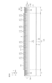
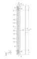
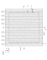
- FIG. 1 is a plan view showing a SiC semiconductor device according to the first embodiment.
- FIG. 2A is a cross-sectional view taken along line IIA-IIA shown in FIG.
- FIG. 2B is a cross-sectional view taken along line IIB-IIB shown in FIG.
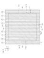
- FIG. 3A is a plan view showing an example of the layout of a chip (first layer).
- FIG. 3B is a plan view showing an example of the layout of the chip (second layer).
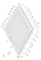
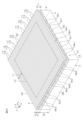
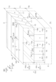
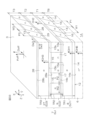
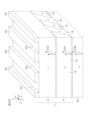
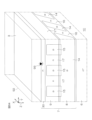
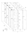
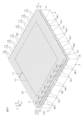
- FIG. 4A is a perspective view showing a chip together with a decorative pattern according to the first embodiment.
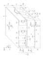
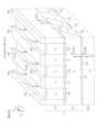
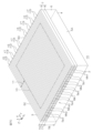
- FIG. 4B is a perspective view showing a chip together with a decorative pattern according to the first embodiment.
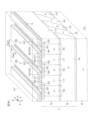
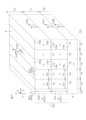
- FIG. 5 is a perspective view of a main part showing a decorative pattern.
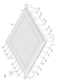
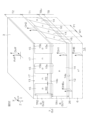
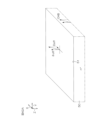
- FIG. 6A is a perspective view showing a chip together with a decorative pattern according to a second embodiment.
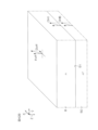
- FIG. 6B is a perspective view showing a chip together with a decorative pattern according to the third embodiment.
- FIG. 6C is a perspective view showing a chip together with a decorative pattern according to the fourth embodiment.
- FIG. 6D is a perspective view showing a chip together with a decorative pattern according to the fifth embodiment.
- FIG. 7 is a cross-sectional perspective view showing a first basic form of a column region.
- FIG. 8A is a plan view showing a first layout example of the first basic embodiment.
- FIG. 8B is a plan view showing a second layout example of the first basic embodiment.
- FIG. 9 is a cross-sectional perspective view showing a second basic form of the column region.
- FIG. 8A is a plan view showing a first layout example of the first basic embodiment.
- FIG. 8B is a plan view showing a second layout example of the first basic embodiment.
- FIG. 10A is a plan view showing a first layout example of the second basic embodiment.
- FIG. 10B is a plan view showing a second layout example of the second basic embodiment.
- FIG. 11 is a cross-sectional perspective view showing the third basic form of the column region.
- FIG. 12A is a plan view showing a first layout example of the third basic embodiment.
- FIG. 12B is a plan view showing a second layout example of the third basic embodiment.
- FIG. 12C is a plan view showing a third layout example of the third basic embodiment.
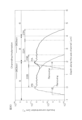
- FIG. 13A is a graph showing an example of a concentration gradient in the second region (first region).
- FIG. 13B is a graph showing an example of the concentration gradient in the second region (first region).
- FIG. 13C is a graph showing an example of the concentration gradient in the second region (first region).
- FIG. 13D is a graph showing an example of the concentration gradient in the second region (first region).
- FIG. 13E is a graph showing an example of the concentration gradient in the second region (first region).
- FIG. 14 is a graph showing a comparative example of the concentration gradient in the second region (first region).
- FIG. 15 is a cross-sectional perspective view showing a column region according to the first embodiment.
- FIG. 16 is a graph showing an example of the concentration gradient in the column region shown in FIG.
- FIG. 17 is a cross-sectional perspective view showing a column region according to the second embodiment.
- FIG. 18 is a graph showing an example of the concentration gradient in the column region shown in FIG. FIG.
- FIG. 19 is a cross-sectional perspective view showing a column region according to the third embodiment.
- FIG. 20 is a graph showing an example of the concentration gradient in the column region shown in FIG.
- FIG. 21 is a cross-sectional perspective view showing a column region according to the fourth embodiment.
- FIG. 22 is a graph showing an example of the concentration gradient in the column region shown in FIG.
- FIG. 23 is a cross-sectional perspective view showing a column region according to the fifth embodiment.
- FIG. 24 is a graph showing an example of the concentration gradient in the column region shown in FIG.
- FIG. 25 is a cross-sectional perspective view showing a column region according to the sixth embodiment.
- FIG. 26 is a graph showing an example of the concentration gradient in the column region shown in FIG. FIG.
- FIG. 27 is a cross-sectional perspective view showing a column region according to the seventh embodiment.
- FIG. 28 is a graph showing an example of the concentration gradient in the column region shown in FIG.
- FIG. 29 is a cross-sectional perspective view showing a column region according to the eighth embodiment.
- FIG. 30 is a graph showing an example of the concentration gradient in the column region shown in FIG.
- FIG. 31 is a cross-sectional perspective view showing a column region according to the ninth embodiment.
- FIG. 32 is a cross-sectional perspective view showing a column region according to the tenth embodiment.
- FIG. 33 is a cross-sectional perspective view showing a column region according to the eleventh embodiment.
- FIG. 34 is a cross-sectional perspective view showing a column region according to the twelfth embodiment.
- FIG. 35 is a plan view showing a main part of an active region.
- FIG. 36 is a cross-sectional perspective view showing a gate structure according to the first embodiment.
- FIG. 37 is a perspective view showing the configuration of the outer circumferential area.
- FIG. 38A is a cross-sectional view showing a main part of the outer circumferential region.
- FIG. 38B is a cross-sectional view showing a main part of the outer circumferential region.
- FIG. 39 is a cross-sectional perspective view showing a gate structure according to the second embodiment.
- FIG. 40 is a schematic diagram showing a wafer used in the manufacture of a SiC semiconductor device.
- FIG. 41 is a flowchart showing an example of a method for manufacturing a SiC semiconductor device.
- FIG. 42A is a cross-sectional perspective view showing an example of a manufacturing method for a SiC semiconductor device.
- FIG. 42B is a cross-sectional perspective view showing a step subsequent to that of FIG. 42A.
- FIG. 42C is a cross-sectional perspective view showing a step subsequent to FIG. 42B.
- FIG. 42D is a cross-sectional perspective view showing a step subsequent to FIG. 42C.
- FIG. 42E is a cross-sectional perspective view showing a step subsequent to FIG. 42D.
- FIG. 42F is a cross-sectional perspective view showing a step subsequent to FIG. 42E.
- FIG. 42G is a cross-sectional perspective view showing a step subsequent to FIG. 42F.
- FIG. 42H is a cross-sectional perspective view showing a step subsequent to FIG. 42G.
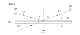
- FIG. 43A is a schematic diagram for explaining the crystal orientation measurement process.
- FIG. 43B is a schematic diagram for explaining the crystal orientation measurement process.
- FIG. 44A is a schematic diagram for explaining the ion implantation step.
- FIG. 44B is a schematic diagram for explaining the ion implantation step.
- FIG. 45 is a plan view showing a SiC semiconductor device according to the second embodiment.
- 46A is a cross-sectional view taken along line XLVIA-XLVIA shown in FIG. 45.
- FIG. 46B is a cross-sectional view taken along line XLVIB-XLVIB shown in FIG. 45.
- FIG. 47A is a plan view showing an example of the layout of a chip (first layer).
- FIG. 47B is a plan view showing an example layout of the chip (second layer).
- FIG. 48 is a perspective view showing an example of a chip layout.
- FIG. 49 is a plan view showing a main part of an active region.
- FIG. 50 is a cross-sectional perspective view showing a gate structure according to the first embodiment.
- FIG. 51 is a perspective view showing the configuration of the outer circumferential area.
- FIG. 52A is a cross-sectional view showing a main part of the outer circumferential region.
- FIG. 52B is a cross-sectional view showing a main part of the outer circumferential region.
- FIG. 53 is a cross-sectional perspective view showing a gate structure according to the second embodiment.
- FIG. 54 is a cross-sectional perspective view showing a gate structure according to the third embodiment.
- FIG. 55 is a sectional perspective view showing a gate structure according to the fourth embodiment.
- FIG. 56 is a cross-sectional perspective view showing a gate structure according to the fifth embodiment.
- FIG. 57 is a plan view showing a SiC semiconductor device according to the third embodiment.
- 58A is a cross-sectional view taken along line LVIIIA-LVIIIA shown in FIG. 57.
- FIG. 58B is a cross-sectional view taken along line LVIIIB-LVIIIB shown in FIG. 57.
- FIG. FIG. 59A is a plan view showing an example of a chip layout.
- FIG. 59B is a plan view showing an example of a chip layout.
- FIG. 59A is a plan view showing an example of a chip layout.
- FIG. 60 is a perspective view showing an example of a chip layout.
- FIG. 61 is a perspective view showing the configuration of the outer circumferential area.
- FIG. 62 is a cross-sectional perspective view showing a diode structure according to the first embodiment.
- FIG. 63 is a cross-sectional perspective view showing a diode structure according to the second embodiment.
- FIG. 64 is a cross-sectional perspective view showing a diode structure according to the third embodiment.
- FIG. 65 is a cross-sectional perspective view showing a diode structure according to the fourth embodiment.
- FIG. 66 is a cross-sectional perspective view showing a diode structure according to the fifth embodiment.
- FIG. 67 is a perspective view showing a chip together with a decorative pattern according to the first modified example.
- FIG. 68 is a perspective view showing a chip together with a decorative pattern according to the second modified example.
- FIG. 69 is a perspective view showing a chip together with a decorative pattern according to the third modified example.
- FIG. 70 is a perspective view showing a chip together with a decorative pattern according to the fourth modified example.
- FIG. 71 is a cross-sectional perspective view showing a column region according to a modified example.
- FIG. 72 is a cross-sectional view showing a main part of the outer circumferential region.
- this term includes a numerical value (shape) that is equal to the numerical value (shape) of the comparison target, as well as a numerical error (shape error) within a range of ⁇ 10% based on the numerical value (shape) of the comparison target.
- shape a numerical value that is equal to the numerical value (shape) of the comparison target
- error a numerical error within a range of ⁇ 10% based on the numerical value (shape) of the comparison target.
- the conductivity type of a semiconductor is indicated using “p-type” or “n-type”, but “p-type” may also be referred to as the “first conductivity type” and “n-type” as the “second conductivity type”. Of course, “n-type” may also be referred to as the “first conductivity type” and “p-type” as the “second conductivity type”.
- p-type is a conductivity type resulting from a trivalent element
- n-type is a conductivity type resulting from a pentavalent element.
- the trivalent element is at least one of boron, aluminum, gallium, and indium.
- the pentavalent element is at least one of nitrogen, phosphorus, arsenic, antimony, and bismuth.
- FIG. 1 is a plan view showing a SiC semiconductor device 1A according to the first embodiment.
- FIG. 2A is a cross-sectional view taken along line IIA-IIA shown in FIG. 1.
- FIG. 2B is a cross-sectional view taken along line IIB-IIB shown in FIG. 1.
- FIG. 3A is a plan view showing an example layout of a chip 2 (first layer 8).
- FIG. 3B is a plan view showing an example layout of a chip 2 (second layer 9).
- FIG. 4A is a perspective view showing a chip 2 together with a decorative pattern PT according to the first embodiment.
- FIG. 4B is a perspective view showing a chip 2 together with a decorative pattern PT according to the first embodiment.
- Figure 5 is a perspective view of a key portion showing the decorative pattern PT.
- Figure 6A is a perspective view showing the chip 2 together with the decorative pattern PT according to the second embodiment.
- Figure 6B is a perspective view showing the chip 2 together with the decorative pattern PT according to the third embodiment.
- Figure 6C is a perspective view showing the chip 2 together with the decorative pattern PT according to the fourth embodiment.
- Figure 7 is a cross-sectional perspective view showing a key portion of the chip 2 together with the first basic form of the column region 12.
- SiC semiconductor device 1A includes chip 2 including SiC single crystal.
- Chip 2 may be referred to as a "SiC chip” or a “semiconductor chip".
- chip 2 is made of hexagonal SiC single crystal and is formed in a rectangular parallelepiped shape.
- the hexagonal SiC single crystal has multiple polytypes including 2H (Hexagonal)-SiC single crystal, 4H-SiC single crystal, 6H-SiC single crystal, etc.
- chip 2 is made of 4H-SiC single crystal, but chip 2 may be made of other polytypes.
- the first main surface 3 and the second main surface 4 are preferably formed by the c-plane of the SiC single crystal.
- the first main surface 3 is formed by the silicon surface ((0001) surface) of the SiC single crystal
- the second main surface 4 is formed by the carbon surface ((000-1) surface) of the SiC single crystal.
- the second side 5B is connected to the first side 5A
- the third side 5C is connected to the second side 5B
- the fourth side 5D is connected to the first side 5A and the third side 5C.
- the first side 5A and the third side 5C extend in a first direction X along the first main surface 3 and face a second direction Y that intersects (specifically, perpendicular to) the first direction X.
- the second side 5B and the fourth side 5D extend in the second direction Y and face the first direction X.
- the first direction X is the a-axis direction ([11-20] direction) of the SiC single crystal
- the second direction Y is the m-axis direction ([1-100] direction) of the SiC single crystal.
- the first side surface 5A and the third side surface 5C are each formed by the m-plane ((1-100) plane) of the SiC single crystal.
- the second side surface 5B and the fourth side surface 5D are each formed by the a-plane ((11-20) plane) of the SiC single crystal.
- the a-plane is a crystal plane perpendicular to the a-axis direction
- the m-plane is a crystal plane perpendicular to the m-axis direction.
- the first direction X may be the m-axis direction of the SiC single crystal
- the second direction Y may be the a-axis direction of the SiC single crystal.
- the first to fourth side surfaces 5A to 5D may each be a ground surface.
- the first to fourth side surfaces 5A to 5D may each be a cleavage surface.
- the XY plane including the first direction X and the second direction Y forms a horizontal plane perpendicular to the vertical direction Z.
- the axis extending along the vertical direction Z may be referred to as the "vertical axis.”
- the first direction X and the second direction Y may be referred to as the "horizontal direction.”
- the horizontal direction is also the direction extending along the first main surface 3.
- the chip 2 (first main surface 3 and second main surface 4) has an off angle ⁇ off inclined at a predetermined angle in a predetermined off direction Doff with respect to the c-plane of the SiC single crystal.
- the c-axis ((0001) axis) of the SiC single crystal is inclined by the off angle ⁇ off from the vertical axis toward the off direction Doff.
- the c-plane of the SiC single crystal is inclined by the off angle ⁇ off with respect to the horizontal plane.
- the off-direction Doff is preferably the a-axis direction of the SiC single crystal (i.e., the first direction X).
- the off-angle ⁇ off may be greater than 0° and less than or equal to 10°.
- the off-angle ⁇ off may have a value that falls within any one of the following ranges: greater than 0° and less than or equal to 1°, 1° or more and less than or equal to 2.5°, 2.5° or more and less than or equal to 5°, 5° or more and less than or equal to 7.5°, and 7.5° or more and less than or equal to 10°.
- the off angle ⁇ off is preferably 5° or less. It is particularly preferable that the off angle ⁇ off is 2° or more and 4.5° or less.
- the off angle ⁇ off is typically set in the range of 4° ⁇ 0.1°. Of course, this specification does not exclude a configuration in which the off angle ⁇ off is 0° (i.e., a configuration in which the first main surface 3 is a just plane relative to the c-plane).
- the chip 2 includes an n-type base layer 6 made of SiC single crystal.
- the base layer 6 may also be referred to as a "base SiC layer", a “base region”, etc.
- the base layer 6 extends in a layered manner in the horizontal direction and forms part of the second main surface 4 and the first to fourth side surfaces 5A to 5D.
- the base layer 6 is made of a substrate made of SiC single crystal (i.e., a SiC substrate).
- the base layer 6 has the off direction Doff and off angle ⁇ off described above.
- the base layer 6 has a base axis channel CHB along the stacking direction.
- the base axis channel CHB is a region (channel) in which the interatomic distance (atomic spacing) is relatively wide with respect to the SiC single crystal that constitutes the base layer 6, and is surrounded by atomic rows that form a crystal axis that extends in the stacking direction (crystal growth direction).
- the base axis channel CHB is a region in which the atomic rows are sparse extending in the stacking direction, and the atomic rows (atomic distance/atomic density) in the horizontal direction are sparse in plan view.
- the base axis channel CHB is preferably a region surrounded by atomic rows along low-index crystal axes among the crystal axes.
- the low-index crystal axes are crystal axes in which the absolute values of "a1", “a2", “a3” and “c" are all expressed as 2 or less (preferably 1 or less) with respect to the Miller indices (a1, a2, a3, c) (the same applies hereinafter in this specification).
- the base axis channel CHB is composed of a region surrounded by atomic rows along the c-axis ((0001) axis) of the SiC single crystal.
- the base axis channel CHB extends along the c-axis and has the off-direction Doff and off-angle ⁇ off described above.
- the base axis channel CHB is inclined from the vertical axis toward the off-direction Doff by the off-angle ⁇ off.
- the base layer 6 may have a peak n-type impurity concentration of 1 ⁇ 10 18 cm ⁇ 3 or more and 1 ⁇ 10 21 cm ⁇ 3 or less.
- the base layer 6 preferably has an almost constant n-type impurity concentration in the thickness direction.
- the n-type impurity concentration of the base layer 6 is preferably adjusted by a single type of pentavalent element. It is particularly preferable that the n-type impurity concentration of the base layer 6 is adjusted by a pentavalent element other than phosphorus. In this embodiment, the n-type impurity concentration of the base layer 6 is adjusted by nitrogen.
- the base layer 6 has a base thickness TB.
- the base thickness TB may be 5 ⁇ m or more and 300 ⁇ m or less.
- the base thickness TB may have a value belonging to any one of the following ranges: 5 ⁇ m or more and 50 ⁇ m or less, 50 ⁇ m or more and 100 ⁇ m or less, 100 ⁇ m or more and 150 ⁇ m or less, 150 ⁇ m or more and 200 ⁇ m or less, 200 ⁇ m or more and 250 ⁇ m or less, and 250 ⁇ m or more and 300 ⁇ m or less.
- the base thickness TB is preferably 50 ⁇ m or more and 250 ⁇ m or less.
- the first layer 8 has a lower end and an upper end.
- the lower end of the first layer 8 is the starting point of crystal growth, and the upper end of the first layer 8 is the end point of crystal growth. Since the first layer 8 is grown continuously from the base layer 6, the lower end of the first layer 8 coincides with the upper end of the base layer 6.
- the boundary between the base layer 6 and the first layer 8 is not necessarily visible, and can be indirectly evaluated and/or determined from other configurations or elements.
- the first layer 8 has an off-direction Doff and an off-angle ⁇ off that are approximately the same as the off-direction Doff and off-angle ⁇ off of the base layer 6.
- the first layer 8 has a first axis channel CH1 along the stacking direction.
- the first axis channel CH1 is a region (channel) in which the interatomic distance (atomic spacing) is relatively wide with respect to the SiC single crystal that constitutes the first layer 8, and is surrounded by atomic rows along a crystal axis that extends in the stacking direction (crystal growth direction).
- the second layer 9 has a second thickness T2.
- the second thickness T2 is preferably less than the base thickness TB.
- the second thickness T2 may be approximately equal to the first thickness T1 or may be different from the first thickness T1.
- the second thickness T2 may be greater than the first thickness T1 or may be less than the first thickness T1.
- the decorative pattern PT includes at least one (in this embodiment, multiple) first mark Mk1 and at least one (in this embodiment, multiple) second mark Mk2.
- the decorative pattern PT does not necessarily have to include both the first mark Mk1 and the second mark Mk2 at the same time, and may consist of only one of the first mark Mk1 and the second mark Mk2.
- the multiple first marks Mk1 are formed on the first side 5A so as to be biased toward a lower range on the lower side of the laminated portion 7 in the thickness direction relative to an upper range on the upper side of the laminated portion 7 in the thickness direction. If the upper range is defined as the first thickness range, the lower range is defined as the second thickness range. If the lower range is defined as the first thickness range, the upper range is defined as the second thickness range. The upper range is the portion of the first to fourth sides 5A to 5D consisting of the second layer 9, and the lower range is the portion of the first to fourth sides 5A to 5D consisting of the first layer 8.
- the first marks Mk1 each extend in a vertically elongated columnar shape along the stacking direction, and together with the first spaces Sp1 on the first side surface 5A, form a stripe mark extending in the stacking direction.
- the first marks Mk1 extend along the first axial channel CH1 on the surface layer of the first side surface 5A.
- the multiple second marks Mk2 are formed on the second side surface 5B so as to be biased toward the upper range relative to the lower range.
- the multiple second marks Mk2 are arranged at intervals in the second direction Y in the upper range, and define multiple n-type second spaces Sp2 each consisting of a part of the laminate 7.
- the multiple second marks Mk2 are each formed in a portion of the second layer 9 on the second side surface 5B, and the multiple second spaces Sp2 each consist of a part of the second layer 9.
- the multiple second marks Mk2 form a pn junction with the multiple second spaces Sp2.
- the upper end of the second mark Mk2 may be formed at a distance from the upper end of the second layer 9 (i.e., the first main surface 3) toward the lower end, and may face the upper end of the second layer 9 across a part (upper end) of the second layer 9.
- the upper end of the second mark Mk2 may be exposed from the upper end of the second layer 9 (i.e., the first main surface 3).
- the second difference mark Md2 has a portion exposed from a corner of the first side surface 5A and a corner of the third side surface 5C.
- the second difference mark Md2 is formed at a corner of the first side surface 5A (third side surface 5C) at a distance in the first direction X from the outermost first mark Mk1, and faces the outermost first mark Mk1 in the first direction X.
- the second difference mark Md2 is formed in a portion of the second side surface 5B made of the first layer 8, and defines a plurality of second spaces Sp2 together with the plurality of second marks Mk2.
- the second difference mark Md2 has a lower end on the lower end side of the first layer 8 and an upper end on the upper end side of the first layer 8.
- the lower end of the second difference mark Md2 is located in a region on the lower end side of the first layer 8 with respect to the intermediate part of the thickness range of the first layer 8
- the upper end of the second difference mark Md2 is located in a region on the upper end side of the first layer 8 with respect to the intermediate part of the thickness range of the first layer 8.
- the second difference mark Md2 consists of a single impurity region having a thickness (depth) that crosses the intermediate part of the first layer 8 along the first axial channel CH1.
- the upper end of the second difference mark Md2 may be formed at a distance from the upper end of the first layer 8 (i.e., the second layer 9) toward the lower end, and may face multiple second marks Mk2 across a portion (upper end) of the first layer 8.
- the upper end of the second difference mark Md2 may be exposed from the upper end of the first layer 8 (i.e., the first main surface 3).
- the upper end of the second difference mark Md2 may be connected to the lower ends of the second marks Mk2.
- the upper end of the second difference mark Md2 may be formed at a distance from the lower ends of the second marks Mk2 toward the lower end of the first layer 8, and may face the second marks Mk2 across a part (lower end) of the first layer 8.
- the SiC semiconductor device 1A includes a p-type column region 12 formed in the stacked portion 7 at least in the active region 10.
- the column region 12 may also be referred to as a "column layer,” a “pillar layer (region),” a “p-type layer (region),” a “p-type zone,” or the like.
- the column region 12 is formed in a three-dimensional lattice shape within the stacked portion 7, and defines a three-dimensional lattice-shaped n-type drift region 13 made up of a part of the stacked portion 7.
- the column region 12 is formed in at least one of the multiple semiconductor layers that make up the stacked portion 7, and forms a superjunction structure SJ with the drift region 13 within the stacked portion 7.
- the column region 12 has a stacked structure that includes multiple p-type first regions 14 and multiple p-type second regions 15.
- the first regions 14 are formed in the first layer 8 at intervals in the horizontal direction, and define a plurality of n-type first drift regions 16, each of which is made up of a part of the first layer 8.
- the first regions 14, together with the first drift regions 16, form a plurality of first pn junctions having charge balance.
- a state of charge balance means a state in which, for multiple adjacent first regions 14, the depletion layer extending from one first pn junction and the depletion layer extending from the other first pn junction are connected within the multiple first drift regions 16.
- the multiple first regions 14 are arranged at intervals in the first array direction Da1 in the first layer 8, and are each formed in a strip shape extending in the first extension direction De1.
- the first extension direction De1 is a direction that intersects or is perpendicular to the first array direction Da1.
- the multiple first regions 14 are formed in a stripe shape extending in the first extension direction De1
- the multiple first drift regions 16 are formed in a stripe shape extending in the first extension direction De1.
- the multiple first regions 14 are extended from the active region 10 to the peripheral region 11 (see FIG. 3A). That is, the multiple first regions 14 are extended from a portion of the first layer 8 located within the active region 10 to a portion of the first layer 8 located within the peripheral region 11.
- the multiple first regions 14 are also arranged at intervals in the first array direction Da1 in the peripheral region 11, and are each formed in a band shape extending in the first extension direction De1.
- the portions of the multiple first regions 14 exposed from the first side surface 5A form multiple first marks Mk1 on the first side surface 5A
- the portions of the multiple first regions 14 exposed from the third side surface 5C form multiple first marks Mk1 on the third side surface 5C.
- the multiple first regions 14 include either or both of the multiple first marks Mk1 as exposed portions exposed from the first side surface 5A and the multiple first marks Mk1 as exposed portions exposed from the third side surface 5C.
- the multiple first marks Mk1 are each formed using a portion (exposed portion) of the multiple first regions 14.
- the layout (exposed locations and arrangement direction) of the multiple first marks Mk1 on the first side 5A (third side 5C) is appropriately adjusted depending on the layout (first arrangement direction Da1 and first extension direction De1) of the multiple first regions 14.
- the multiple first regions 14 have an off direction Doff and an off angle ⁇ off that are approximately the same as the off direction Doff and the off angle ⁇ off of the first axis channel CH1. In other words, the multiple first regions 14 are inclined by the off angle ⁇ off from the vertical axis toward the off direction Doff.
- the distance between the lower end of the first layer 8 and the first lower end 14a may be 0 ⁇ m or more and 2 ⁇ m or less.
- the distance between the lower end of the first layer 8 and the first lower end 14a may have a value that falls within any one of the ranges of 0 ⁇ m or more and 0.5 ⁇ m or less, 0.5 ⁇ m or more and 1 ⁇ m or less, 1 ⁇ m or more and 1.5 ⁇ m or less, and 1.5 ⁇ m or more and 2 ⁇ m or less.
- the first lower end 14a may have an extension that crosses the boundary between the base layer 6 and the first layer 8 and is located within the base layer 6.
- the thickness of the extension of the first lower end 14a based on the upper end of the base layer 6 may be greater than 0 ⁇ m and less than 2 ⁇ m.
- the thickness of the extension of the first lower end 14a may have a value that belongs to any one of the following ranges: greater than 0 ⁇ m and less than 0.5 ⁇ m, 0.5 ⁇ m or more and less than 1 ⁇ m, 1 ⁇ m or more and less than 1.5 ⁇ m, and 1.5 ⁇ m or more and less than 2 ⁇ m.
- the first upper end 14b may be formed at a distance from the upper end of the first layer 8 (i.e., the second layer 9) toward the lower end, and may face the upper end of the first layer 8 across a portion (upper end) of the first layer 8.
- the first upper end 14b may be substantially coincident with the upper end of the first layer 8 and connected to the second layer 9.
- the distance between the upper end of the first layer 8 and the first upper end 14b may be 0 ⁇ m or more and 1 ⁇ m or less.
- the distance between the upper end of the first layer 8 and the first upper end 14b may have a value that falls within any one of the ranges of 0 ⁇ m or more and 0.25 ⁇ m or less, 0.25 ⁇ m or more and 0.5 ⁇ m or less, 0.5 ⁇ m or more and 0.75 ⁇ m or less, and 0.75 ⁇ m or more and 1 ⁇ m or less.
- the first region thickness TR1 is preferably 1 ⁇ m or more.
- the first region thickness TR1 is preferably 5 ⁇ m or less.
- the first region thickness TR1 may have a value that falls within any one of the following ranges: 1 ⁇ m or more and 1.5 ⁇ m or less, 1.5 ⁇ m or more and 2 ⁇ m or less, 2 ⁇ m or more and 2.5 ⁇ m or less, 2.5 ⁇ m or more and 3 ⁇ m or less, 3 ⁇ m or more and 3.5 ⁇ m or less, 3.5 ⁇ m or more and 4 ⁇ m or less, 4 ⁇ m or more and 4.5 ⁇ m or less, and 4.5 ⁇ m or more and 5 ⁇ m or less.
- the second regions 15 and the second layer 9 form a second superjunction structure SJ2.
- the charge balance state means that, for adjacent second regions 15, the depletion layer extending from one second pn junction and the depletion layer extending from the other second pn junction are connected within the second drift regions 17.
- the multiple second regions 15 intersect with the multiple first regions 14 in a planar view.
- the multiple second drift regions 17 are connected in a lattice pattern to the multiple first drift regions 16 at the boundary between the first layer 8 and the second layer 9, and together with the multiple first drift regions 16 form a single three-dimensional lattice-shaped drift region 13.
- the multiple second drift regions 17 form a three-dimensional lattice-shaped current path together with the multiple first drift regions 16.
- the portions of the multiple second regions 15 exposed from the second side surface 5B form multiple second marks Mk2 on the second side surface 5B
- the portions of the multiple second regions 15 exposed from the fourth side surface 5D form multiple second marks Mk2 on the fourth side surface 5D.
- the multiple second regions 15 include either or both of the multiple second marks Mk2 as exposed portions exposed from the second side surface 5B and the multiple second marks Mk2 as exposed portions exposed from the fourth side surface 5D.
- the multiple second marks Mk2 are each formed using a portion (exposed portion) of the multiple second regions 15.
- the layout (exposed locations and arrangement direction) of the multiple second marks Mk2 on the second side 5B (fourth side 5D) is appropriately adjusted depending on the layout (second arrangement direction Da2 and second extension direction De2) of the multiple second regions 15.
- the second regions 15 each have a second lower end 15a at the lower end of the second layer 9 and a second upper end 15b at the upper end of the second layer 9.
- the second lower end 15a is located in a region on the lower end side of the second layer 9 relative to the intermediate part of the thickness range of the second layer 9, and the second upper end 15b is located in a region on the upper end side of the second layer 9 relative to the intermediate part of the thickness range of the second layer 9.
- the second regions 15 each consist of a single impurity region having a thickness (depth) that crosses the intermediate part of the second layer 9 along the second axial channel CH2.
- the second regions 15 each have a second region thickness TR2 (region depth).
- the second region thickness TR2 may be less than the second thickness T2 of the second layer 9.
- the second region thickness TR2 may be greater than the second thickness T2.
- the second region thickness TR2 may be approximately equal to the second thickness T2.
- the second pitch P2 may be 0.1 ⁇ m or more and 5 ⁇ m or less.
- the second pitch P2 may have a value that belongs to any one of the following ranges: 0.1 ⁇ m or more and 0.25 ⁇ m or less, 0.25 ⁇ m or more and 0.5 ⁇ m or less, 0.5 ⁇ m or more and 0.75 ⁇ m or less, 0.75 ⁇ m or more and 1 ⁇ m or less, 1 ⁇ m or more and 1.5 ⁇ m or less, 1.5 ⁇ m or more and 2 ⁇ m or less, 2 ⁇ m or more and 2.5 ⁇ m or less, 2.5 ⁇ m or more and 3 ⁇ m or less, 3 ⁇ m or more and 3.5 ⁇ m or less, 3.5 ⁇ m or more and 4 ⁇ m or less, 4 ⁇ m or more and 4.5 ⁇ m or less, and 4.5 ⁇ m or more and 5 ⁇ m or less.
- the second pitch P2 is preferably 0.5 ⁇ m or more and 1.5 ⁇ m or less.
- the decorative pattern PT (multiple first marks Mk1 and multiple second marks Mk2) is formed in a layout according to the example layout of the first region 14 and the second region 15 shown below.
- the first arrangement direction Da1 of the first regions 14 may be the a-axis direction (first direction X), and the first extension direction De1 of the first regions 14 may be the m-axis direction (second direction Y).
- first direction X the first direction
- second direction Y the first extension direction De1 intersects (specifically, is perpendicular to) the off-direction Doff of the first layer 8
- the multiple first regions 14 are inclined by approximately the off angle ⁇ off from the vertical axis toward the off-direction Doff in a cross-sectional view seen from the m-plane ((1-100) plane) of the SiC single crystal.
- the m-plane of the SiC single crystal is a crystal plane perpendicular to the m-axis direction.
- the multiple second regions 15 extend in approximately the vertical direction Z in a cross-sectional view seen from the a-plane ((11-20) plane) of the SiC single crystal.
- the a-plane of the SiC single crystal is perpendicular to the a-axis direction.
- the multiple second regions 15 are inclined by approximately the off angle ⁇ off from the vertical axis toward the off-direction Doff in a cross-sectional view seen from the m-plane of the SiC single crystal.
- the second regions 15 may intersect the first regions 14 non-orthogonally in a planar view. That is, the second arrangement direction Da2 of the second regions 15 may be a direction other than the m-axis direction and the a-axis direction, and the second extension direction De2 of the second regions 15 may be a direction other than the m-axis direction and the a-axis direction.
- the second arrangement direction Da2 intersects with both the first arrangement direction Da1 and the first extension direction De1
- the second extension direction De2 intersects with both the first arrangement direction Da1 and the first extension direction De1.
- the second extension direction De2 intersects with the off-direction Doff of the second layer 9.
- the second extension direction De2 may be inclined from the a-axis toward one side (left side of the paper) or the other side (right side of the paper) of the m-axis in a plan view.
- the second regions 15 have a second extension direction De2 that forms an extension angle ⁇ a with the a-axis when the a-axis is set as the reference (0°).
- the second regions 15 may be orthogonal to the first regions 14 in a plan view. That is, the second array direction Da2 of the second regions 15 may be the a-axis direction (second direction Y), and the second extension direction De2 of the second regions 15 may be the m-axis direction (first direction X). In this case, the second array direction Da2 coincides with the first extension direction De1 and is orthogonal to the first array direction Da1. Also, the second extension direction De2 coincides with the first array direction Da1 and is orthogonal to the first extension direction De1.
- the second extension direction De2 intersects (specifically, is perpendicular to) the off direction Doff of the second layer 9, so that the second regions 15 are inclined by approximately the off angle ⁇ off from the vertical axis toward the off direction Doff in a cross-sectional view seen from the m-plane of the SiC single crystal.
- the second regions 15 may intersect the first regions 14 non-orthogonally in a planar view. That is, the second array direction Da2 of the second regions 15 may be a direction other than the a-axis direction and the m-axis direction, and the second extension direction De2 of the second regions 15 may be a direction other than the a-axis direction and the m-axis direction.
- the second array direction Da2 intersects with both the first array direction Da1 and the first extension direction De1
- the second extension direction De2 intersects with both the first array direction Da1 and the first extension direction De1.
- the second extension direction De2 intersects with the off direction Doff of the second layer 9.
- the column region 12 may have the configurations shown in Figures 11, 12A, 12B, and 12C.
- Figure 11 is a cross-sectional perspective view showing a third basic configuration of the column region 12.
- Figures 12A, 12B, and 12C are plan views showing first, second, and third layout examples of the column region 12 according to the third basic configuration.
- the first region 14 is indicated by dashed lines, and the second region 15 is indicated by hatching.
- the gradual decrease portion 22 has a thickness of 0.8 ⁇ m or more and 1.1 ⁇ m or less, and has a concentration decrease rate of 50% or less within this thickness range.
- the p-type impurity concentration of the gradual decrease portion 22 is within a concentration range of 3.5 ⁇ 10 16 cm -3 or more and 7 ⁇ 10 16 cm -3 or less.
- the p-type impurity concentration of the gradually decreasing portion 23 gradually decreases from the gradual decrease portion 22 to 1 ⁇ 10 15 cm -3 .
- the first upper end 14b of the first region 14 is formed at a distance from the upper end (second layer 9) of the first layer 8 toward the lower end, and faces the second layer 9 across a part (upper end) of the first layer 8.
- the first gradually increasing portion 20A, the first peak portion 21A, the first gradual portion 22A, and the first gradually decreasing portion 23A of the first region 14 are located within the first layer 8.
- the second upper end 15b of the second region 15 is formed at a distance from the upper end (first main surface 3) of the second layer 9 toward the lower end, and faces the first main surface 3 across a part (upper end) of the second layer 9.
- the second gradually increasing portion 20B, the second peak portion 21B, the second gradual portion 22B, and the second gradually decreasing portion 23B of the second region 15 are located within the second layer 9.
- the first arrangement direction Da1 is the a-axis direction (first direction X), and the first extension direction De1 is the m-axis direction (second direction Y).
- the arrangement direction and extension direction of the multiple intermediate regions 25 are changed according to the first arrangement direction Da1 and first extension direction De1 of the multiple first regions 14. Therefore, the first arrangement direction Da1 may be the m-axis direction, and the first extension direction De1 may be the a-axis direction.
- the first arrangement direction Da1 may be a direction other than the a-axis direction and the m-axis direction
- the first extension direction De1 may be a direction other than the a-axis direction and the m-axis direction.
- the intermediate regions 25, together with the first regions 14, are drawn out from the active region 10 to the peripheral region 11.
- the intermediate regions 25 are drawn out from a portion of the first layer 8 located within the active region 10 to a portion of the first layer 8 located within the peripheral region 11.
- the intermediate regions 25 are also arranged at intervals in the first array direction Da1 in the peripheral region 11, and are each formed in a strip shape extending in the first extension direction De1.
- the region element 25a is composed of a random impurity region introduced into the surface layer of the first layer 8 by a random injection method into the first layer 8 (see also FIG. 14). In other words, the region element 25a is not formed in the second layer 9. Furthermore, the region element 25a has a thickness in the direction along the first axial channel CH1 that is less than the first region thickness TR1 of the first region 14. Furthermore, the thickness of the region element 25a is less than the second region thickness TR2 of the second region 15.
- the region element 25a does not have a gradual portion 22 having a thickness of 0.5 ⁇ m or more, and has a concentration gradient including a gradually increasing portion 20, a peak portion 21, and a gradually decreasing portion 23 in a range of 0.5 ⁇ m.
- each intermediate region 25 has multiple peak portions 21 (peak value P) according to the number of multiple region elements 25a in the thickness direction of the first layer 8.
- the intermediate regions 25 each have an intermediate width WM.
- the intermediate width WM is a width along the first arrangement direction Da1. It is preferable that the intermediate width WM is less than the first thickness T1 of the first layer 8. Of course, the intermediate width WM may be equal to or greater than the first thickness T1. It is preferable that the intermediate width WM is less than the second thickness T2 of the second layer 9. Of course, the intermediate width WM may be equal to or greater than the second thickness T2.
- the intermediate width WM is approximately equal to the first width W1 of the first region 14.
- the intermediate width WM may be greater than or equal to the first width W1, or less than the first width W1. It is preferable that the intermediate width WM is greater than or equal to 1 ⁇ m. It is preferable that the intermediate width WM is less than or equal to 5 ⁇ m.
- the intermediate regions 25 are formed at an intermediate pitch PM interval in the first arrangement direction Da1. It is preferable that the intermediate pitch PM is approximately equal to the first pitch P1 of the first region 14. Of course, the intermediate pitch PM may be equal to or greater than the first pitch P1, or may be less than the first pitch P1. For clarity, an intermediate pitch PM greater than the first pitch P1 is shown in FIG. 25.
- the intermediate pitch PM may be 0.1 ⁇ m or more and 5 ⁇ m or less.
- the intermediate pitch PM may have a value that belongs to any one of the following ranges: 0.1 ⁇ m or more and 0.25 ⁇ m or less, 0.25 ⁇ m or more and 0.5 ⁇ m or less, 0.5 ⁇ m or more and 0.75 ⁇ m or less, 0.75 ⁇ m or more and 1 ⁇ m or less, 1 ⁇ m or more and 1.5 ⁇ m or less, 1.5 ⁇ m or more and 2 ⁇ m or less, 2 ⁇ m or more and 2.5 ⁇ m or less, 2.5 ⁇ m or more and 3 ⁇ m or less, 3 ⁇ m or more and 3.5 ⁇ m or less, 3.5 ⁇ m or more and 4 ⁇ m or less, 4 ⁇ m or more and 4.5 ⁇ m or less, and 4.5 ⁇ m or more and 5 ⁇ m or less.
- the intermediate pitch PM is preferably 0.5 ⁇ m or more and 1.5 ⁇ m or less.
- the second region 15 preferably has an extension located within the first layer 8 and is connected to the intermediate region 25 within the first layer 8.
- the second region 15 preferably is electrically connected to the first region 14 via the intermediate region 25 within the first layer 8.
- the second region 15 forms one drift region 13 that extends continuously in the stacking direction together with the first region 14 and the intermediate region 25.
- the extension of the second region 15 may be connected to both the intermediate region 25 and the first region 14 within the first layer 8.
- the concentration gradient in the region between the first region 14 and the second region 15 is mitigated by the intermediate region 25, improving the accuracy of the charge balance.
- FIG. 27 is a cross-sectional perspective view showing the column region 12 according to the seventh embodiment.
- FIG. 28 is a graph showing an example of the concentration gradient of the column region 12 shown in FIG. 27.
- the column region 12 according to the seventh embodiment has a shape obtained by modifying the first region 14 according to the first to sixth embodiments.
- the second region 15 according to the seventh embodiment may have a shape similar to any one of the shapes of the second region 15 according to the first to sixth embodiments.
- the first region 14 is exposed from the upper end of the first layer 8.
- the first region 14 does not have part or all of the first gradually increasing portion 20A.
- Figure 28 shows an example in which the first region 14 does not have all of the first gradually increasing portion 20A and the first peak portion 21A. That is, in this example, the first upper end 14b includes the first gradual portion 22A exposed from the upper end of the first layer 8.
- the first region 14 has a first peak value PA at the upper end of the first layer 8, and has a concentration gradient that gradually decreases toward the lower end of the first layer 8.
- the first upper end 14b includes a part of the first gradually increasing portion 20A or a part of the first peak portion 21A, and a part of the first gradually increasing portion 20A or a part of the first peak portion 21A may be exposed from the upper end of the first layer 8.
- the second region 15 has an extension located within the first layer 8 and is connected to the first region 14 within the first layer 8.
- the concentration gradient formed in the region between the first region 14 and the second region 15 is mitigated by the exposed portion of the first region 14, improving the accuracy of the charge balance.
- Such a configuration can be obtained by partially removing the upper end of the first layer 8 after the formation of the first region 14 until part or all of the first gradually increasing portion 20A of the first region 14 disappears.
- the upper end of the first layer 8 may be partially removed by a grinding method.
- the grinding method may be a mechanical polishing method and/or a chemical mechanical polishing method.
- the upper end of the first layer 8 is composed of a ground surface, and the first region 14 is exposed from the ground surface.
- the second layer 9 is laminated on top of the ground surface of the first layer 8.
- the upper end of the first layer 8 may be partially removed by an etching method.
- the etching method may be a wet etching method and/or a dry etching method.
- the upper end of the first layer 8 is an etched surface, and the first region 14 is exposed from the etched surface.
- the second layer 9 is laminated on top of the etched surface of the first layer 8.
- FIG. 29 is a cross-sectional perspective view showing the column region 12 according to the eighth embodiment.
- FIG. 30 is a graph showing an example of a concentration gradient in the column region 12 shown in FIG. 29.
- the column region 12 according to the eighth embodiment has a form obtained by modifying the second region 15 according to the first to seventh embodiments.
- the first region 14 according to the eighth embodiment may have a form similar to any one of the forms of the first region 14 according to the first to seventh embodiments.
- the first region 14 according to the seventh embodiment is shown.
- the second region 15 has a second peak value PB at the upper end of the second layer 9, and has a concentration gradient that gradually decreases toward the lower end of the second layer 9.
- the second upper end 15b includes a part of the second gradually increasing portion 20B or a part of the second peak portion 21B, and a part of the second gradually increasing portion 20B or a part of the second peak portion 21B may be exposed from the upper end of the second layer 9.
- the configuration in which the second region 15 is exposed from the upper end of the second layer 9 is effective when a device structure is formed using the second layer 9 (first main surface 3) and the second region 15 is used to adjust the electrical characteristics of the device structure.
- Such a configuration can be obtained by partially removing the upper end of the second layer 9 after the formation of the second region 15 until part or all of the second gradually increasing portion 20B of the second region 15 disappears.
- the upper end (first main surface 3) of the second layer 9 may be partially removed by a grinding method.
- the grinding method may be a mechanical polishing method and/or a chemical mechanical polishing method.
- the upper end of the second layer 9 is composed of a ground surface, and the second region 15 is exposed from the ground surface.
- Fig. 31 is a cross-sectional perspective view showing the column region 12 according to the ninth embodiment.
- Fig. 32 is a cross-sectional perspective view showing the column region 12 according to the tenth embodiment.
- the stacked portion 7 may have a stacked structure including a buffer layer 26, a first layer 8, and a second layer 9 stacked in this order from the base layer 6 side.
- the buffer layer 26 may be referred to as a "buffer SiC layer", a "buffer region”, etc.
- the buffer layer 26 includes SiC single crystals and has n-type conductivity.
- the buffer layer 26 is stacked on the base layer 6.
- the buffer layer 26 extends in a layered manner in the horizontal direction, forming the middle part of the chip 2 and forming part of the first to fourth side surfaces 5A to 5D.
- the buffer layer 26 is made of an epitaxial layer (i.e., a SiC epitaxial layer) that is crystal-grown starting from the base layer 6.
- the buffer layer 26 has a lower end and an upper end.
- the lower end of the buffer layer 26 is the starting point of crystal growth, and the upper end of the buffer layer 26 is the end point of crystal growth. Since the buffer layer 26 is grown continuously from the base layer 6, the lower end of the buffer layer 26 coincides with the upper end of the base layer 6.
- the boundary between the base layer 6 and the buffer layer 26 is not necessarily visible, and can be indirectly evaluated and/or determined from other configurations and elements.
- the buffer layer 26 has an off-direction Doff and an off-angle ⁇ off that are approximately the same as the off-direction Doff and off-angle ⁇ off of the base layer 6.
- the buffer layer 26 has a buffer axis channel CHBu along the stacking direction.
- the buffer axis channel CHBu is a region (channel) in which the interatomic distance (atomic spacing) is relatively wide with respect to the SiC single crystal that constitutes the buffer layer 26, and is surrounded by atomic rows along the crystal axis that extends in the stacking direction (crystal growth direction).
- the buffer axis channel CHBu is a region in which the atomic rows extend in the stacking direction and the atomic rows (atomic distance/atomic density) in the horizontal direction are sparse in a plan view. It is preferable that the buffer axis channel CHBu is a region surrounded by atomic rows along the low-index crystal axis among the crystal axes.
- the buffer layer 26 has an n-type impurity concentration adjusted with at least one pentavalent element.
- the n-type impurity concentration of the buffer layer 26 may be adjusted with at least one of nitrogen, phosphorus, arsenic, antimony, and bismuth. It is preferable that the buffer layer 26 contains a pentavalent element other than phosphorus.
- the n-type impurity concentration of the buffer layer 26 is preferably adjusted with at least nitrogen.
- the buffer layer 26 preferably contains nitrogen and a pentavalent element other than nitrogen.
- the buffer layer 26 preferably contains either arsenic or antimony, or both, as the pentavalent element other than phosphorus and nitrogen.
- the buffer layer 26 has a buffer thickness TBu.
- the buffer thickness TBu is preferably less than the base thickness TB.
- the buffer thickness TBu is preferably 1 ⁇ m or more.
- the buffer thickness TBu is preferably 5 ⁇ m or less.
- the buffer thickness TBu may have a value that falls within any one of the following ranges: 1 ⁇ m or more and 1.5 ⁇ m or less, 1.5 ⁇ m or more and 2 ⁇ m or less, 2 ⁇ m or more and 2.5 ⁇ m or less, 2.5 ⁇ m or more and 3 ⁇ m or less, 3 ⁇ m or more and 3.5 ⁇ m or less, 3.5 ⁇ m or more and 4 ⁇ m or less, 4 ⁇ m or more and 4.5 ⁇ m or less, and 4.5 ⁇ m or more and 5 ⁇ m or less.
- the first layer 8 is stacked on the buffer layer 26, and the second layer 9 is stacked on the first layer 8.
- the first layer 8 is made of an epitaxial layer (i.e., a SiC epitaxial layer) crystal-grown starting from the buffer layer 26, and has n-type conductivity. Therefore, the first layer 8 has an off-direction Doff and an off-angle ⁇ off that are approximately equal to the off-direction Doff and off-angle ⁇ off of the buffer layer 26.
- the first axis channel CH1 approximately coincides with the buffer axis channel CHBu.
- the first region 14 has a shape similar to any one of the shapes of the first region 14 in the first to eighth embodiment examples, and is formed in the first layer 8.
- the second region 15 has a shape similar to any one of the shapes of the first region 14 in the first to eighth embodiment examples, and is formed in the second layer 9.
- the first lower end 14a of the first region 14 may be formed with a gap from the lower end to the upper end of the first layer 8, and may face the buffer layer 26 across a part (lower end) of the first layer 8.
- the entire area of the first region 14 (first gradually increasing portion 20A, first peak portion 21A, first gradually decreasing portion 22A, and first gradually decreasing portion 23A) may be located within the first layer 8.
- the first lower end 14a may be approximately coincident with the lower end of the first layer 8 and connected to the buffer layer 26.
- the first lower end 14a may have an extension that crosses the boundary between the buffer layer 26 and the first layer 8 and is located within the buffer layer 26. Since the first axial channel CH1 is approximately coincident with the buffer axial channel CHBu, the extension of the first lower end 14a is formed along the buffer axial channel CHBu within the buffer layer 26.
- the extension of the first lower end 14a is preferably located on the upper end side of the buffer layer 26 relative to the middle part of the thickness range of the buffer layer 26.
- the extension of the first lower end 14a includes the first gradually tapering portion 23A.
- the extension of the first lower end 14a may include a part of the first gradual portion 22A and the first gradually tapering portion 23A.
- the third layer 27 has a lower end and an upper end.
- the lower end of the third layer 27 is the starting point of crystal growth, and the upper end of the third layer 27 is the end point of crystal growth. Since the third layer 27 is grown continuously from the second layer 9, the lower end of the third layer 27 coincides with the upper end of the second layer 9.
- the boundary between the second layer 9 and the third layer 27 is not necessarily visible, and can be indirectly evaluated and/or determined from other configurations or elements.
- the third layer 27 has an off direction Doff and an off angle ⁇ off that are approximately the same as the off direction Doff and the off angle ⁇ off of the second layer 9.
- the third layer 27 has a third axis channel CH3 along the stacking direction.
- the third axis channel CH3 is a region (channel) in which the interatomic distance (atomic spacing) is relatively wide with respect to the SiC single crystal that constitutes the third layer 27, and is surrounded by atomic rows along the crystal axis that extends in the stacking direction (crystal growth direction).
- the third axis channel CH3 is a region in which the atomic rows extend in the stacking direction and the atomic rows (atomic distance/atomic density) in the horizontal direction are sparse in a planar view. It is preferable that the third axis channel CH3 is a region surrounded by atomic rows along the low-index crystal axis among the crystal axes.
- the n-type impurity concentration of the third layer 27 is preferably lower than the n-type impurity concentration of the base layer 6.
- the third layer 27 may have a peak n-type impurity concentration of 1 ⁇ 10 15 cm -3 or more and 1 ⁇ 10 18 cm -3 or less.
- the n-type impurity concentration of the third layer 27 may be approximately constant in the thickness direction.
- the n-type impurity concentration of the third layer 27 may have a concentration gradient that gradually increases and/or gradually decreases in the stacking direction (crystal growth direction).
- the third layer 27 has an n-type impurity concentration adjusted by at least one pentavalent element.
- the n-type impurity concentration of the third layer 27 may be adjusted by at least one of nitrogen, phosphorus, arsenic, antimony, and bismuth. It is preferable that the third layer 27 contains a pentavalent element other than phosphorus.
- the n-type impurity concentration of the third layer 27 is preferably adjusted with at least nitrogen.
- the third layer 27 preferably contains nitrogen and a pentavalent element other than nitrogen.
- the third layer 27 preferably contains either arsenic or antimony, or both, as the pentavalent element other than phosphorus and nitrogen.
- the third thickness T3 is preferably 1 ⁇ m or more.
- the third thickness T3 is preferably 5 ⁇ m or less.
- the third thickness T3 may have a value that falls within any one of the following ranges: 1 ⁇ m or more and 1.5 ⁇ m or less, 1.5 ⁇ m or more and 2 ⁇ m or less, 2 ⁇ m or more and 2.5 ⁇ m or less, 2.5 ⁇ m or more and 3 ⁇ m or less, 3 ⁇ m or more and 3.5 ⁇ m or less, 3.5 ⁇ m or more and 4 ⁇ m or less, 4 ⁇ m or more and 4.5 ⁇ m or less, and 4.5 ⁇ m or more and 5 ⁇ m or less.
- the multiple third regions 28 and the third layer 27 form a third superjunction structure SJ3.
- the state of charge balance means that, for multiple adjacent third regions 28, the depletion layer extending from one third pn junction and the depletion layer extending from the other third pn junction are connected within the multiple third drift regions 29.
- the multiple third regions 28 are drawn from the active region 10 to the peripheral region 11. That is, the multiple third regions 28 are drawn from a portion of the third layer 27 located within the active region 10 to a portion of the third layer 27 located within the peripheral region 11.
- the multiple third regions 28 are also arranged at intervals in the third array direction Da3 in the peripheral region 11, and are each formed in a band shape extending in the third extension direction De3.
- the multiple third marks are each formed using a portion (exposed portion) of the multiple third regions 28.
- the multiple third marks partition multiple third spaces on the first side surface 5A (third side surface 5C).
- the multiple third marks and multiple third spaces are formed on the first side surface 5A (third side surface 5C) in the same layout as the multiple first marks Mk1 and multiple first spaces Sp1.
- the third regions 28 each have a third lower end 28a at the lower end of the third layer 27 and a third upper end 28b at the upper end of the third layer 27.
- the third lower end 28a is located in a region on the lower end side of the third layer 27 relative to the intermediate part of the thickness range of the third layer 27, and the third upper end 28b is located in a region on the upper end side of the third layer 27 relative to the intermediate part of the thickness range of the third layer 27.
- the third regions 28 each consist of a single impurity region having a thickness (depth) that crosses the intermediate part of the third layer 27 along the third axial channel CH3.
- the third lower end 28a may be formed with a gap from the lower end of the third layer 27 toward the upper end, and may face the second layer 9 across a portion (lower end) of the third layer 27.
- the third lower end 28a may be substantially coincident with the lower end of the third layer 27 and connected to the second layer 9.
- the third upper end 28b may be formed at a distance from the upper end of the third layer 27 (i.e., the first main surface 3) toward the lower end, and may face the upper end of the third layer 27 across a portion (upper end) of the third layer 27.
- the third upper end 28b may be exposed from the upper end of the third layer 27 (i.e., the first main surface 3).
- the distance between the upper end of the third layer 27 and the third upper end 28b may be 0 ⁇ m or more and 1 ⁇ m or less.
- the distance between the upper end of the third layer 27 and the third upper end 28b may have a value that falls within any one of the ranges of 0 ⁇ m or more and 0.25 ⁇ m or less, 0.25 ⁇ m or more and 0.5 ⁇ m or less, 0.5 ⁇ m or more and 0.75 ⁇ m or less, and 0.75 ⁇ m or more and 1 ⁇ m or less.
- the plurality of third regions 28 may have a peak p-type impurity concentration of 1 ⁇ 10 15 cm ⁇ 3 or more and 1 ⁇ 10 18 cm ⁇ 3 or less.
- the p-type impurity concentration (peak value) of the third regions 28 may be equal to or more than the p-type impurity concentration (peak value) of the first region 14.
- the p-type impurity concentration (peak value) of the third regions 28 may be less than the p-type impurity concentration (peak value) of the first region 14. It is preferable that the p-type impurity concentration (peak value) of the third regions 28 is approximately equal to the p-type impurity concentration (peak value) of the first region 14.
- the p-type impurity concentration of the third region 28 is preferably adjusted by at least one trivalent element. It is particularly preferable that the p-type impurity concentration of the third region 28 is adjusted by a trivalent element that is heavier than carbon. In other words, the third region 28 preferably contains a trivalent element other than boron (at least one of aluminum, gallium, and indium). In this embodiment, the p-type impurity concentration of the third region 28 is adjusted by aluminum.
- the multiple third regions 28 each have a third region thickness TR3.
- the third region thickness TR3 may be less than the third thickness T3 of the third layer 27.
- the third region thickness TR3 may be greater than the third thickness T3.
- the third region thickness TR3 may be approximately equal to the third thickness T3.
- the body regions 32 are made of random impurity regions introduced into the surface layer of the second layer 9 by a random implantation method into the second layer 9 (see also FIG. 14). Therefore, the body regions 32 have a thickness in the direction along the second axial channel CH2 that is less than the second region thickness TR2 of the second region 15. The thickness of the body regions 32 is less than the first region thickness TR1 of the first region 14.
- the multiple field regions 38 are preferably formed at a pitch different from the second pitch P2 of the second region 15 (the first pitch P1 of the first region 14). It is particularly preferable that the pitch of the multiple field regions 38 is larger than the second pitch P2 (the first pitch P1). Of course, the pitch of the multiple field regions 38 may be smaller than the second pitch P2 (the first pitch P1). Also, the pitch of the multiple field regions 38 may be approximately equal to the second pitch P2 (the first pitch P1).
- the SiC semiconductor device 1A includes a plurality of contact openings 43 formed in the interlayer insulating film 40.
- the plurality of contact openings 43 include a plurality of contact openings 43 (not shown) that expose a plurality of gate structures 35 (gate electrodes 37), and a plurality of contact openings 43 that expose a plurality of source regions 33.
- the plurality of contact openings 43 for the source regions 33 are formed in the regions between the plurality of adjacent gate structures 35, and expose the plurality of source regions 33 and the plurality of contact regions 34.
- each gate structure 35 may face multiple first drift regions 16 in the stacking direction.
- the multiple gate structures 35 may be arranged offset from the multiple first regions 14 in the first array direction Da1 and face either one or both of the first regions 14 and the first drift regions 16 in the stacking direction.
- the arrangement direction of the multiple gate structures 35 may be a direction other than the first arrangement direction Da1 and the second arrangement direction D2.
- the extension direction of the multiple gate structures 35 may be a direction other than the first extension direction De1 and the second extension direction De2.
- the multiple gate structures 35 may intersect both the multiple first regions 14 and the multiple second regions 15 in a planar view. In this case, a configuration in which the arrangement direction of the multiple gate structures 35 is one of the a-axis direction and the m-axis direction, and the extension direction of the multiple gate structures 35 is the other of the a-axis direction and the m-axis direction, is not prevented.
- the multiple gate structures 35 are each arranged to straddle two adjacent body regions 32, and each cover the multiple source regions 33 located in one and the other body region 32. In addition, the multiple gate structures 35 each face the multiple second regions 15 (second regions 15) and the multiple second drift regions 17 in the stacking direction.
- the mark 54 may include either or both of a first orientation flat extending in the m-axis direction and a second orientation flat extending in the a-axis direction.
- the mark 54 may include either or both of an orientation notch recessed in the m-axis direction and an orientation notch recessed in the a-axis direction.
- Figure 40 shows an orientation flat extending in the a-axis direction in a plan view.
- a plurality of device regions 55 and a plurality of cutting lines 56 are set on the wafer 50 by alignment marks or the like.
- Each device region 55 corresponds to the SiC semiconductor device 1A.
- Each of the plurality of device regions 55 is set to have a rectangular shape in a plan view.
- the multiple device regions 55 are set in a matrix along the first direction X and the second direction Y in a plan view.
- the multiple device regions 55 are each set at intervals inward from the periphery of the first wafer main surface 51 in a plan view.
- the multiple cutting lines 56 are set in a lattice extending along the first direction X and the second direction Y to partition the multiple device regions 55.
- FIG. 41 is a flow chart showing an example of a method for manufacturing a SiC semiconductor device 1A.
- FIG. 42A to FIG. 42H are cross-sectional perspective views showing an example of a method for manufacturing a SiC semiconductor device 1A.
- FIG. 43A to FIG. 43B are schematic diagrams for explaining the crystal orientation measurement process.
- FIG. 44A to FIG. 44B are schematic diagrams for explaining the ion implantation process.
- FIG. 42A to FIG. 42H show cross-sectional perspective views of a portion of an active region 10 of one device region 55.
- step S1 in FIG. 41 the aforementioned wafer 50 preparation process is performed (step S1 in FIG. 41).
- a determination process is performed as to whether or not an n-type buffer layer 26 (see FIG. 31 and FIG. 32) formation process is performed (step S2 in FIG. 41). If a buffer layer 26 is to be formed (step S2 in FIG. 41: YES), the buffer layer 26 is formed starting from the first wafer main surface 51 (wafer 50) by epitaxial growth (step S3 in FIG. 41). If a buffer layer 26 formation process is not performed (step S2 in FIG. 41: NO), this process is omitted.
- the crystal orientation of the first layer 8 includes a process for measuring the off angle ⁇ off of the first layer 8. In other words, this process includes a process for measuring the crystal orientation of the first axis channel CH1 of the first layer 8.
- the X-ray diffraction device 57 includes an irradiation unit 58 and a detection unit 59, and performs the rocking curve measurement method.
- the irradiation unit 58 irradiates the incident X-ray L1 having a predetermined incident angle ⁇ with respect to the upper end of the first layer 8 (the first wafer main surface 51 of the wafer 50).
- the incident angle ⁇ is defined as the angle between the incident X-ray L1 and the upper end of the first layer 8 (the first wafer main surface 51 of the wafer 50).
- the rocking curve measurement method is performed only at one location (e.g., the center) of the upper end of the first layer 8 (first wafer main surface 51 of the wafer 50). If in-plane variation in the off angle ⁇ off is expected, the rocking curve measurement method may be performed at multiple locations (e.g., the center and peripheral areas) of the upper end of the first layer 8 (first wafer main surface 51 of the wafer 50).
- the fourth measurement point Po4 is set on the periphery of the first layer 8 at a distance from the first measurement point Po1 to the other side in the second direction Y (the side toward the mark 54).
- the fifth measurement point Po5 is set on the periphery of the first layer 8 at a distance from the first measurement point Po1 to the other side in the first direction X (to the left of the mark 54).
- the measurement results of the incident angle ⁇ , diffraction angle 2 ⁇ , and off angle ⁇ off at the first to fifth measurement points Po1 to Po5 are shown in the following Table 1.
- the off angle ⁇ off is calculated using the incident angle ⁇ and diffraction angle 2 ⁇ by the formula " ⁇ -(2 ⁇ 1/2)".
- the average value of the off angle ⁇ off of the first to fifth measurement points Po1 to Po5 was 4.036°, and the standard deviation of these off angles ⁇ off was 0.009° ( ⁇ 0.01°). From this, it can be understood that the in-plane variation of the off angle ⁇ off occurring at the upper end of the first layer 8 (first wafer main surface 51 of wafer 50) is extremely small, and is not enough to interfere with the channeling implantation process.
- the measurement point may be any one or more (all) of the first to fifth measurement points Po1 to Po5.
- the measurement point may be only the first measurement point Po1.
- the off angle ⁇ off may be measured at multiple points on the upper end of the first layer 8 (first wafer main surface 51 of the wafer 50) and an implantation angle may be set in the channeling implantation process according to the in-plane variation of the off angle ⁇ off.
- the manufacturing man-hours manufactured costs
- the in-plane error of the first region 14 formed in the first layer 8 is appropriately suppressed.
- the off-angle ⁇ off of the first layer 8 is approximately equal to the off-angle ⁇ off of the wafer 50 and the off-angle ⁇ off of the buffer layer 26. Therefore, the crystal orientation measurement process may be performed on the wafer 50 or the buffer layer 26 prior to the formation process of the first layer 8. However, from the standpoint of ensuring accuracy, it is preferable that the crystal orientation measurement process be performed on the first layer 8.
- the intermediate regions 25 are arranged at intervals in the first arrangement direction Da1 across the entire area of the first layer 8, and are each formed to extend in a strip shape in the first extension direction De1. In other words, the intermediate regions 25 are formed in stripes so as to cross the device regions 55 and the cutting lines 56 in the first extension direction De1. After the process of forming the intermediate regions 25, the mask (not shown) is removed.
- the process of forming the multiple intermediate regions 25 may be performed consecutively from the process of forming the multiple first regions 14. In this case, the multiple intermediate regions 25 may be formed using the above-mentioned first mask 60.
- the wafer 50 may be supported horizontally and the trivalent element may be introduced into the second layer 9 along the second axial channel CH2.
- the wafer 50 may be supported tilted by the off angle ⁇ off from the horizontal and the trivalent element may be introduced into the second layer 9 along the second axial channel CH2.
- a plurality of second regions 15 having a predetermined thickness are formed at a predetermined depth (see also Figures 13A to 13E).
- the implantation energy of the trivalent element may be 100 KeV or more and 2000 KeV or less.
- the implantation energy may have a value that belongs to any one of the following ranges: 100 KeV or more and 250 KeV or less, 250 KeV or more and 500 KeV or less, 500 KeV or more and 750 KeV or less, 750 KeV or more and 1000 KeV or less, 1000 KeV or more and 1250 KeV or less, 1250 KeV or more and 1500 KeV or less, 1500 KeV or more and 1750 KeV or less, and 1750 KeV or more and 2000 KeV or less.
- the injection energy for the second region 15 may be approximately equal to the injection energy for the first region 14, or may be different from the injection energy for the first region 14.
- the injection energy for the second region 15 may be equal to or greater than the injection energy for the first region 14.
- the injection energy for the second region 15 may also be less than the injection energy for the first region 14.
- the injection temperature of the trivalent element may be adjusted in the range of 0°C to 1500°C.
- the injection temperature may have a value that belongs to any one of the following ranges: 0°C to 25°C, 25°C to 50°C, 50°C to 100°C, 100°C to 250°C, 250°C to 500°C, 500°C to 750°C, 750°C to 1000°C, 1000°C to 1250°C, and 1250°C to 1500°C.
- the trivalent element is introduced along the second axial channel CH2, in which the atomic rows are relatively sparse in plan view.
- the trivalent element travels through the second axial channel CH2 while repeatedly undergoing small-angle scattering due to the channeling effect, and reaches a relatively deep position in the second layer 9.
- the probability of the trivalent element colliding with the atomic rows of the SiC single crystal is reduced.
- a trivalent element belonging to the heavy elements heavier than carbon is introduced into the second layer 9.
- the trivalent element is a trivalent element other than boron (at least one of aluminum, gallium, and indium).
- the trivalent element is aluminum.
- the trivalent element is introduced into the second layer 9 through the second openings 63 at an angle of approximately the off angle ⁇ off with respect to the upper end of the second layer 9 in a cross-sectional view along the second arrangement direction Da2.
- the second extension direction De2 is also a direction other than the a-axis direction and the m-axis direction.
- the multiple first regions 14 have a first extension angle ⁇ 1 inclined toward one side of the m-axis with respect to the a-axis
- the multiple second regions 15 have a second extension angle ⁇ 2 toward the other side of the m-axis with respect to the a-axis.
- the first extension angle ⁇ 1 may be +45° ⁇ 5° and the second extension angle ⁇ 2 may be -45° ⁇ 5° (see FIG. 12A).
- the first extension angle ⁇ 1 may be +30° ⁇ 5° and the second extension angle ⁇ 2 may be -30° ⁇ 5° (see FIG. 12B).
- the first extension angle ⁇ 1 may be +60° ⁇ 5° and the second extension angle ⁇ 2 may be -60° ⁇ 5° (see FIG. 12C).
- the annealing method for the second regions 15 may also serve as the annealing method for the first regions 14 described above. In this case, the annealing method for the first regions 14 before the process of forming the second regions 15 may be omitted.
- a determination step is performed as to whether or not a thickness adjustment step for the second layer 9 is to be performed (step S15 in FIG. 41). If the thickness of the second layer 9 is to be adjusted (step S15 in FIG. 41: YES), the second layer 9 is thinned from the upper end side (step S16 in FIG. 41).
- the thickness adjustment process may include a process of partially removing the upper end of the second layer 9 by a grinding method.
- the grinding method may be a mechanical polishing method and/or a chemical mechanical polishing method.
- the thinning process of the second layer 9 may include a process of partially removing the upper end of the second layer 9 by an etching method.
- the etching method may be a wet etching method and/or a dry etching method.
- the thickness adjustment process may include a step of exposing the second regions 15 from the upper end of the second layer 9 (see also Figures 27 to 30, etc.). In other words, the thickness adjustment process may include a step of removing part or all of the second gradually increasing portions 20B of the second regions 15. If the thickness adjustment process is not performed (Step S15 in Figure 41: NO), this step is omitted.
- step S11 in FIG. 41 a process similar to step S11 in FIG. 41 may be carried out to form a plurality of intermediate regions 25 in the surface layer portion of the second layer 9 (see also FIGS. 25 and 26). If the process of forming the further superjunction structure SJ is not carried out (step S17 in FIG. 41: NO), this process is omitted.
- a determination step is performed as to whether or not the top layer 30 (see also FIG. 34) formation step is performed (step S19 in FIG. 41). If the top layer 30 formation step is performed (step S19 in FIG. 41: YES), the top layer 30 is formed starting from the second layer 9 by epitaxial growth (step S20 in FIG. 41). If the top layer 30 formation step is not performed (step S19 in FIG. 41: NO), this step is omitted.
- the wafer 50 is cut along the multiple planned cutting lines 56.
- the portions of the multiple first regions 14 located on the multiple planned cutting lines 56 are exposed from the first side 5A (third side 5C) as multiple first marks Mk1.
- the portions of the multiple intermediate regions 25 located on the multiple planned cutting lines 56 are exposed from the first side 5A (third side 5C) as parts (upper ends) of the multiple first marks Mk1.
- the portions of the multiple second regions 15 located on the multiple planned cutting lines 56 are exposed from the second side 5B (fourth side 5D) as multiple second marks Mk2.
- the multiple modified layers are formed in the thickness range of the wafer 50 (base layer 6) relative to the thickness range of the laminated portion 7. Specifically, it is preferable that the multiple modified layers are formed in the wafer 50 (base layer 6) at intervals from the thickness range of the laminated portion 7 toward the second wafer main surface 52 of the wafer 50.
- multiple modified layers are formed (remain) on the portions of the first to fourth side surfaces 5A to 5D that are made of the base layer 6 after cleavage. This makes it possible to prevent the multiple modified layers from overlapping the decorative pattern PT (the multiple first marks Mk1 and the multiple second marks Mk2). This improves the visibility of the decorative pattern PT. In addition, the electrical influence that the multiple modified layers have on the multiple first regions 14 and the multiple second regions 15 via the decorative pattern PT is reduced.
- the first to fourth side surfaces 5A to 5D each consist of a cleavage surface and each have a plurality of modified layers. Therefore, the plurality of modified layers may be regarded as one component of the SiC semiconductor device 1A (chip 2).
- step S2 may be determined in advance at the stage of the wafer 50 preparation step (step S1 in FIG. 41).
- the SiC semiconductor device 1A may be manufactured along a predetermined manufacturing line. Through steps including those described above, multiple SiC semiconductor devices 1A are manufactured from one wafer 50.
- the multiple second regions 15 are exposed from at least one of the first to fourth connection surfaces 73A to 73D that is perpendicular to the second extension direction De2. In this embodiment, the multiple second regions 15 are exposed from both the second connection surface 73B and the fourth connection surface 73D.
- the bottom of the well region 78 is located closer to the lower end of the second layer 9 than the bottom wall of the gate structure 35. It is preferable that the bottom of the well region 78 is located closer to the outer circumferential surface 72 than the second lower ends 15a of the second regions 15. It is particularly preferable that the bottom of the well region 78 is located closer to the outer circumferential surface 72 than the intermediate portions of the thickness ranges of the second regions 15.
- Well region 78 differs from second region 15 etc. in that it does not have a gradual portion 22 having a thickness of 0.5 ⁇ m or more, and has a concentration gradient in a range of 0.5 ⁇ m that includes a gradually increasing portion 20, a peak portion 21 and a gradually decreasing portion 23.
- Well region 78 may have a peak value of a p-type impurity concentration of 1 ⁇ 10 15 cm ⁇ 3 or more and 1 ⁇ 10 18 cm ⁇ 3 or less.
- the multiple field regions 38 are arranged at intervals from the periphery of the active surface 71 (first to fourth connection surfaces 73A to 73D) and the periphery of the chip 2 (first to fourth side surfaces 5A to 5D). Specifically, the multiple field regions 38 are arranged at intervals from the well region 78 to the periphery side of the outer circumferential surface 72.
- the multiple field regions 38 extend in a band shape along the active surface 71 in a plan view, and are formed in a ring shape (specifically a square ring shape) surrounding the active surface 71.
- the multiple field regions 38 overlap the column regions 12 in the stacking direction on the outer peripheral surface 72. That is, the multiple field regions 38 are formed in a region above multiple intersections of the multiple first regions 14 and the multiple second regions 15. The multiple field regions 38 intersect with the multiple second regions 15 in the portion extending in the first extension direction De1 in a plan view, and intersect with the multiple first regions 14 in the portion extending in the second extension direction De2.
- the bottoms of the multiple field regions 38 are preferably located on the outer peripheral surface 72 side relative to the middle part of the thickness range of the second region 15.
- the multiple field regions 38 may be connected to the multiple second regions 15 in the portion extending along the second extension direction De2.
- the multiple field regions 38 may be formed horizontally spaced apart from the multiple second regions 15 in the portion extending along the second extension direction De2, and may not be connected to the multiple second regions 15.
- the second insulating film 42 selectively covers the active surface 71, the outer peripheral surface 72, and the first to fourth connection surfaces 73A to 73D, sandwiching the first insulating film 41 between them.
- the second insulating film 42 covers the multiple gate structures 35 in the active region 10.
- the second insulating film 42 covers the multiple field regions 38 and well regions 78 in the outer peripheral region 11, sandwiching the first insulating film 41 between them.
- the SiC semiconductor device 1B includes a sidewall structure 79 disposed in the interlayer insulating film 40 so as to cover at least one of the first to fourth connection surfaces 73A to 73D.
- the sidewall structure 79 is disposed on the first insulating film 41 and is covered by the second insulating film 42.
- the sidewall structure 79 reduces the step formed between the active surface 71 and the outer peripheral surface 72.
- the sidewall structure 79 is formed in a band shape extending along at least one of the first to fourth connection surfaces 73A to 73D.
- the sidewall structure 79 is formed in a ring shape (specifically, a square ring shape) extending along the first to fourth connection surfaces 73A to 73D so as to surround the active surface 71 in a plan view.
- the sidewall structure 79 may have a portion that extends in a film-like manner along the outer peripheral surface 72, and a portion that extends in a film-like manner along the first to fourth connection surfaces 73A to 73D.
- the sidewall structure 79 is formed at a distance from the innermost field region 38 toward the active surface 71, and faces the multiple second regions 15 and well regions 78 in the horizontal and stacking directions, sandwiching the first insulating film 41 between them.
- the sidewall structure 79 may face the body region 32, sandwiching the first insulating film 41 between them.
- the SiC semiconductor device 1B includes a gate pad 45, a plurality of gate wirings 46, a source pad 47, and a drain pad 48.
- the drain pad 48 is formed in the same manner as in the first embodiment.
- the gate pad 45 is disposed on the active surface 71 at a distance from the outer peripheral surface 72 in a plan view.
- the gate pad 45 is disposed in a region close to the center of one side of the active surface 71 (the second connection surface 73B in this embodiment) in a plan view.
- the gate pad 45 may also be disposed at a corner of the active surface 71 or in the center of the active surface 71 in a plan view.
- the multiple gate wirings 46 are arranged on the active surface 71 at a distance from the outer peripheral surface 72 in a plan view.
- the multiple gate wirings 46 include a first gate wiring 46A and a second gate wiring 46B.
- the first gate wiring 46A is pulled out from the gate pad 45 toward the second connection surface 73B and extends in a line along the periphery of the active surface 71 so as to intersect (specifically, perpendicular to) a portion (specifically, one end) of the multiple gate structures 35.
- the first gate wiring 46A penetrates the interlayer insulating film 40 via the multiple contact openings 43 and is electrically connected to one end of the multiple gate structures 35 (buried electrodes 77).
- the second gate wiring 46B is pulled out from the gate pad 45 toward the fourth connection surface 73D and extends in a line along the periphery of the active surface 71 so as to intersect (specifically, perpendicular to) a portion (specifically, the other end) of the multiple gate structures 35.
- the second gate wiring 46B penetrates the interlayer insulating film 40 via the multiple contact openings 43 and is electrically connected to the other end of the multiple gate structures 35 (buried electrodes 77).
- the source pad 47 is disposed on the active surface 71 at a distance from the outer peripheral surface 72 in a plan view.
- the source pad 47 penetrates the interlayer insulating film 40 via a plurality of contact openings 43, and is electrically connected to the body region 32, the plurality of source regions 33, and the plurality of contact regions 34. In other words, the source pad 47 is electrically connected to the column region 12 via the body region 32.
- FIG. 53 is a cross-sectional perspective view showing a gate structure 35 according to the second embodiment.
- the multiple gate structures 35 according to the first embodiment described above were arranged shifted from the column region 12 (multiple second regions 15) toward the multiple second drift regions 17.
- the multiple gate structures 35 according to the second embodiment are arranged so as to overlap the multiple second regions 15 in the stacking direction.
- the multiple gate structures 35 overlap the multiple second regions 15 in a one-to-one correspondence in the stacking direction.
- the multiple gate structures 35 each have a bottom wall connected to a corresponding second region 15. Specifically, the multiple gate structures 35 are formed wider than the corresponding second region 15, and each have a bottom wall connected to the corresponding second region 15 and a side wall connected to the corresponding second drift region 17.
- FIG. 54 is a cross-sectional perspective view showing a gate structure 35 according to a third embodiment.
- the multiple gate structures 35 according to the third embodiment each have a layout that does not require consideration of misalignment with respect to the multiple second regions 15.
- the multiple gate structures 35 extend in a direction other than the second extension direction De2 so as to intersect with the multiple second regions 15.
- the multiple gate structures 35 are arranged at intervals in the first array direction Da1 of the first region 14 and extend in the first extension direction De1 of the first region 14.
- the first array direction Da1 is the a-axis direction (first direction X)
- the first extension direction De1 is the m-axis direction (second direction Y).
- each gate structure 35 may face multiple first drift regions 16 in the stacking direction.
- the multiple gate structures 35 may be arranged offset from the multiple first regions 14 in the first array direction Da1 and face either one or both of the first regions 14 and the first drift regions 16 in the stacking direction.
- the arrangement direction and extension direction of the multiple gate structures 35 are changed according to the first arrangement direction Da1 and first extension direction De1 of the multiple first regions 14. Therefore, the first arrangement direction Da1 may be the m-axis direction, and the first extension direction De1 may be the a-axis direction. Also, the first arrangement direction Da1 may be a direction other than the a-axis direction and the m-axis direction, and the first extension direction De1 may be a direction other than the a-axis direction and the m-axis direction.
- the arrangement direction of the multiple gate structures 35 may be a direction other than the first arrangement direction Da1 and the second arrangement direction D2.
- the extension direction of the multiple gate structures 35 may be a direction other than the first extension direction De1 and the second extension direction De2.
- the multiple gate structures 35 may intersect both the multiple first regions 14 and the multiple second regions 15 in a planar view.
- the angle (absolute value) between the extension direction of the gate structure 35 and the second extension direction De2 may be greater than 0° and less than 90°.
- the angle (absolute value) of the gate structure 35 may have a value belonging to any one of the ranges of greater than 0° and less than 18°, 18° or more and less than 36°, 36° or more and less than 54°, 54° or more and less than 72°, and 72° or more and less than 90°.
- the angle (absolute value) of the gate structure 35 may be set to a value belonging to any one of the ranges of 30° ⁇ 5°, 45° ⁇ 5°, and 60° ⁇ 5°.
- the buried electrode 77 faces the second regions 15 and the second drift regions 17 across the insulating film 76 in the stacking direction and horizontal direction.
- the source regions 33 and contact regions 34 described above face the second regions 15 and the second drift regions 17 across a portion of the body region 32 in the stacking direction.
- FIG. 55 is a cross-sectional perspective view showing a gate structure 35 according to the fourth embodiment.
- the multiple gate structures 35 according to the fourth embodiment each have a configuration that contributes to narrowing the pitch.
- the multiple gate structures 35 according to the fourth embodiment are particularly effective in realizing a narrower pitch in the column region 12 (multiple second regions 15).
- FIG. 55 shows an example in which the gate structure 35 according to the first embodiment described above is replaced with the gate structure 35 according to the fourth embodiment, but the configuration of the gate structure 35 according to the fourth embodiment is also applicable to the configurations of the gate structures 35 according to the second and third embodiments.
- the multiple gate structures 35 each include a trench 75, an insulating film 76, a buried electrode 77, and a buried insulator 80.
- the trench 75 has a form similar to that of the first embodiment.
- the insulating film 76 is formed at a distance from the first main surface 3 (active surface 71) to the bottom wall side of the trench 75, exposing a surface portion of the first main surface 3 (active surface 71) at the opening end of the trench 75. It is preferable that the upper end of the insulating film 76 is located on the first main surface 3 side relative to the intermediate depth range of the trench 75.
- the buried electrode 77 is buried in the trench 75 at a distance from the first main surface 3 (active surface 71) toward the bottom wall of the trench 75, and defines an open recess that is recessed toward the bottom wall of the trench 75 at the opening end of the trench 75.
- the buried electrode 77 exposes the surface portion of the first main surface 3 (active surface 71) and the upper end of the insulating film 76 at the opening end of the trench 75. It is preferable that the upper end of the buried electrode 77 is located on the first main surface 3 side relative to the middle part of the depth range of the trench 75.
- the buried insulator 80 is buried in the trench 75 (open recess) so as to expose the first principal surface 3 (active surface 71), and covers the insulating film 76 and buried electrode 77 within the trench 75.
- the buried insulator 80 is buried in the trench 75 at a distance from the first principal surface 3 (active surface 71) toward the buried electrode 77, and exposes the surface portion of the first principal surface 3 (active surface 71) at the open end of the trench 75.
- the upper end of the buried insulator 80 is preferably located on the first main surface 3 side relative to the intermediate portion of the depth range of the trench 75.
- the buried insulator 80 may include at least one of a silicon oxide film, a silicon nitride film, and a silicon oxynitride film.
- the buried insulator 80 preferably includes a silicon oxide film.
- the aforementioned multiple source regions 33 are each formed in a region between multiple adjacent gate structures 35 in the surface layer portion of the first main surface 3 (active surface 71).
- the multiple source regions 33 are arranged at intervals along the multiple gate structures 35 so as to be connected to the multiple gate structures 35 located on both sides.
- the multiple source regions 33 arranged along one sidewall of the gate structure 35 face the multiple source regions 33 arranged along the other sidewall of the gate structure 35 in a one-to-one correspondence.
- the multiple source regions 33 are arranged in a matrix in a plan view.
- the multiple source regions 33 on one side may face the regions between the multiple source regions 33 on the other side in a one-to-one correspondence.
- the multiple source regions 33 may be arranged in a staggered pattern in a planar view.
- the multiple source regions 33 have portions exposed from the sidewall of the trench 75 at the opening end of the trench 75, and face the buried electrode 77 and the buried insulator 80 with the insulating film 76 between them.
- the aforementioned contact regions 34 are formed in the regions between adjacent gate structures 35 on the surface layer of the first main surface 3 (active surface 71).
- the contact regions 34 are arranged at intervals along the gate structures 35 so as to be connected to the gate structures 35 located on both sides.
- the multiple contact regions 34 are arranged alternately with the multiple source regions 33 along the multiple gate structures 35. More specifically, the multiple contact regions 34 arranged along one sidewall of the gate structure 35 face the multiple contact regions 34 arranged along the other sidewall of the gate structure 35 in a one-to-one correspondence.
- the multiple source regions 33 are also arranged in a matrix in a planar view.
- the multiple contact regions 34 on one side may face the regions between the multiple source regions 33 on the other side (i.e., the multiple source regions 33) in a one-to-one correspondence.
- the multiple contact regions 34 may be arranged in a staggered pattern in a planar view.
- the multiple contact regions 34 have portions exposed from the sidewall of the trench 75 at the opening end of the trench 75, and face the buried electrode 77 and the buried insulator 80 with the insulating film 76 between them.
- the aforementioned interlayer insulating film 40 has a layered structure including a first insulating film 41 and a second insulating film 42.
- the first insulating film 41 selectively covers the active surface 71, the outer peripheral surface 72, and the first to fourth connection surfaces 73A to 73D.
- the first insulating film 41 covers the peripheral portion of the active surface 71 and exposes the multiple gate structures 35 collectively in the inner portion of the active surface 71. Specifically, the first insulating film 41 is connected to the insulating film 76 at both ends of the multiple gate structures 35, exposing the buried electrodes 77. The first insulating film 41 also covers the outer peripheral surface 72 and the first to fourth connection surfaces 73A to 73D in the same manner as in the first embodiment.
- the second insulating film 42 selectively covers the active surface 71, the outer peripheral surface 72, and the first to fourth connection surfaces 73A to 73D across the first insulating film 41.
- the second insulating film 42 covers the peripheral portion of the active surface 71, exposing the multiple gate structures 35 collectively at the inner portion of the active surface 71.
- the second insulating film 42 penetrates into the trench 75 from above the first main surface 3 (active surface 71) at both ends of the multiple gate structures 35, and is connected to the buried insulator 80 within the trench 75.
- the interlayer insulating film 40 includes a plurality of contact openings 43 (not shown) that expose both ends (buried electrodes 77) of the plurality of gate structures 35, and a single contact opening 43 that collectively exposes the inner portions (buried insulator 80) of the plurality of gate structures 35, the plurality of source regions 33, and the plurality of contact regions 34.
- the source pad 47 is electrically insulated from the multiple gate structures 35 (buried electrodes 77) by the buried insulator 80, and is electrically connected to the multiple source regions 33 and multiple contact regions 34 at the first main surface 3 (active surface 71).
- the source pad 47 has a buried portion buried in the trench 75. The buried portion of the source pad 47 faces the buried electrode 77 within the trench 75 with the buried insulator 80 in between, and is electrically connected to the multiple source regions 33 and multiple contact regions 34 at the opening end of the trench 75.
- FIG. 56 is a cross-sectional perspective view showing a gate structure 35 according to the fifth embodiment.
- the gate structures 35 according to the fifth embodiment each have a configuration that is a modification of the gate structures 35 according to the fourth embodiment.
- the configuration of the gate structure 35 according to the fifth embodiment is also applicable to the configurations of the gate structures 35 according to the first to third embodiments.
- the multiple gate structures 35 each include a trench 75, an insulating film 76, a buried electrode 77, and a buried insulator 80.
- the trench 75 has a similar configuration to that of the first embodiment.
- the insulating film 76 includes an upper insulating film 81 and a lower insulating film 82.
- the upper insulating film 81 is formed as an insulating film for channel control, and covers the wall surface on the opening side of the trench 75 relative to the bottom of the body region 32.
- the upper insulating film 81 has a portion that crosses the boundary between the second drift region 17 and the body region 32 and covers the second drift region 17. In this case, it is preferable that the coverage area of the upper insulating film 81 relative to the body region 32 is larger than the coverage area of the upper insulating film 81 relative to the second drift region 17.
- the upper insulating film 81 may include a silicon oxide film. It is preferable that the upper insulating film 81 includes a silicon oxide film made of an oxide of the chip 2.
- the upper insulating film 81 may have a thickness of 1 nm or more and 100 nm or less. The thickness of the upper insulating film 81 may have a value that belongs to any one of the following ranges: 1 nm or more and 25 nm or less, 25 nm or more and 50 nm or less, 50 nm or more and 75 nm or less, and 75 nm or more and 100 nm or less.
- the lower insulating film 82 covers the wall surface on the bottom wall side of the trench 75 relative to the bottom of the body region 32.
- the lower insulating film 82 covers the second drift region 17.
- the coverage area of the lower insulating film 82 relative to the second drift region 17 is larger than the coverage area of the upper insulating film 81 relative to the body region 32.
- the lower insulating film 82 may include a silicon oxide film.
- the lower insulating film 82 may include a silicon oxide film made of an oxide of the chip 2, or may include a silicon oxide film formed by a CVD method.
- the lower insulating film 82 has a thickness greater than that of the upper insulating film 81.
- the thickness of the lower insulating film 82 is preferably 10 to 50 times the thickness of the upper insulating film 81.
- the lower insulating film 82 may have a thickness of 100 nm or more and 500 nm or less.
- the thickness of the lower insulating film 82 may have a value that belongs to any one of the following ranges: 100 nm or more and 150 nm or less, 150 nm or more and 200 nm or less, 200 nm or more and 250 nm or less, 250 nm or more and 300 nm or less, 300 nm or more and 350 nm or less, 350 nm or more and 400 nm or less, 400 nm or more and 450 nm or less, and 450 nm or more and 500 nm or less.
- the buried electrode 77 has a multi-electrode structure (double electrode structure) including an upper electrode 83, a lower electrode 84, and an intermediate insulating film 85.
- the upper electrode 83 is buried in the opening side of the trench 75 with an insulating film 76 in between.
- the upper electrode 83 is buried in the opening side of the trench 75 with an upper insulating film 81 in between, and faces the body region 32 with the upper insulating film 81 in between.
- the facing area of the upper electrode 83 relative to the body region 32 is larger than the facing area of the upper electrode 83 relative to the second drift region 17.
- the upper electrode 83 is embedded in the trench 75 at a distance from the first main surface 3 (active surface 71) toward the bottom wall of the trench 75, and defines an opening recess that is recessed toward the bottom wall of the trench 75 at the opening end of the trench 75.
- the upper electrode 83 exposes the surface portion of the first main surface 3 (active surface 71) and the upper end of the upper insulating film 81 at the opening end of the trench 75.
- a gate potential is applied to the upper electrode 83 as a control potential.
- the upper electrode 83 controls the inversion and non-inversion of the channel (current path) in the body region 32 in response to the gate potential.
- the upper electrode 83 may include p-type or n-type conductive polysilicon.
- the lower electrode 84 is embedded in the bottom wall side of the trench 75 with the insulating film 76 in between. Specifically, the lower electrode 84 is embedded in the bottom wall side of the trench 75 with the lower insulating film 82 in between, and faces the second drift region 17 with the lower insulating film 82 in between. In other words, the lower electrode 84 is embedded in the bottom wall side of the trench 75 with respect to the bottom of the body region 32. Although specific illustration is omitted, the lower electrode 84 is drawn out to the opening side of the trench 75 in part of the trench 75 (both ends in this embodiment).
- the facing area of the lower electrode 84 with respect to the second drift region 17 is larger than the facing area of the upper electrode 83 with respect to the body region 32.
- the lower electrode 84 extends in a wall shape along the depth direction of the trench 75.
- the lower electrode 84 has an upper end that protrudes from the lower insulating film 82 toward the upper electrode 83, and is engaged with the lower end of the upper electrode 83.
- the upper end of the lower electrode 84 faces the upper insulating film 81 (body region 32) horizontally, sandwiching the lower end of the upper electrode 83 therebetween.
- the lower electrode 84 may be applied with a gate potential or a source potential.
- a gate potential When a gate potential is applied to the lower electrode 84, the lower electrode 84 has the same potential as the upper electrode 83. Therefore, the voltage drop between the upper electrode 83 and the lower electrode 84 is suppressed. This suppresses electric field concentration on the gate structure 35.
- the intermediate insulating film 85 is interposed between the upper electrode 83 and the lower electrode 84, and electrically insulates the upper electrode 83 and the lower electrode 84 within the trench 75.
- the intermediate insulating film 85 is continuous with the upper insulating film 81 and the lower insulating film 82.
- the intermediate insulating film 85 has a thickness smaller than that of the lower insulating film 82.
- the thickness of the intermediate insulating film 85 is preferably greater than that of the upper insulating film 81.
- the intermediate insulating film 85 may include a silicon oxide film.
- the intermediate insulating film 85 preferably includes a silicon oxide film made of an oxide of the lower electrode 84.
- the buried insulator 80 is buried in the trench 75 (open recess) so as to expose the first principal surface 3 (active surface 71), and covers the upper insulating film 81 and the upper electrode 83 within the recess.
- the buried insulator 80 is buried in the trench 75 at a distance from the first principal surface 3 (active surface 71) toward the upper electrode 83, and exposes the surface portion of the first principal surface 3 (active surface 71) at the open end of the trench 75.
- the aforementioned multiple source regions 33 have portions exposed from the sidewall of trench 75 at the opening end of trench 75, and face upper electrode 83 and buried insulator 80 across upper insulating film 81.
- the aforementioned multiple contact regions 34 have portions exposed from the sidewall of trench 75 at the opening end of trench 75, and face upper electrode 83 and buried insulator 80 across upper insulating film 81.
- the aforementioned field regions 38, interlayer insulating film 40, gate pad 45, aforementioned gate wirings 46, aforementioned source pad 47, and aforementioned drain pad 48 have the same configuration as in the second embodiment.
- the multiple gate wirings 46 penetrate the interlayer insulating film 40 via the multiple contact openings 43 and are electrically connected to the multiple upper electrodes 83.
- the multiple gate wirings 46 penetrate the interlayer insulating film 40 via the multiple contact openings 43 and are electrically connected to the multiple upper electrodes 83 and the multiple lower electrodes 84.
- the interlayer insulating film 90 covers the multiple field regions 38 in the peripheral region 11.
- the interlayer insulating film 90 is continuous with the periphery of the first main surface 3 (first to fourth side surfaces 5A to 5D).
- the interlayer insulating film 90 may be formed at a distance inward from the periphery of the first main surface 3, exposing the second layer 9 from the periphery of the first main surface 3.
- the multiple surface regions 95 are arranged at intervals in the second array direction Da2 and are each formed in a strip shape extending in the second extension direction De2. In other words, in this embodiment, the multiple surface regions 95 are arranged in stripes extending along the second extension direction De2 of the multiple second regions 15.
- the p-type impurity concentration of the multiple surface regions 95 is preferably adjusted by at least one trivalent element.
- the trivalent element of the surface region 95 may be the same as the trivalent element of the second region 15, etc., or may be a different species from the trivalent element of the second region 15, etc.
- the trivalent element of the surface region 95 may be at least one of boron, aluminum, gallium, and indium.
- the first pad electrode 92 is mechanically and electrically connected to the top layer 30 on the first main surface 3.
- the first pad electrode 92 forms a JBS structure with the multiple surface layer regions 95 on the first main surface 3, and forms a Schottky junction with the region between the multiple surface layer regions 95 on the first main surface 3.
- the layout restrictions and electrical characteristic restrictions of the JBS structure resulting from the layout of the superjunction structure SJ are alleviated.
- FIG. 66 is a cross-sectional perspective view showing an SBD structure 93 according to the fifth embodiment.
- the SBD structure 93 according to the fifth embodiment has a layout that is a modification of the layout of the multiple surface regions 95 according to the fourth embodiment. Specifically, the multiple surface regions 95 are arranged in stripes in the active region 10 that extend in a direction intersecting the second extension direction De2 of the multiple second regions 15.
- the multiple surface regions 95 are arranged at intervals in the first arrangement direction Da1 of the first region 14 and extend in the first extension direction De1 of the first region 14.
- the first arrangement direction Da1 is the m-axis direction
- the first extension direction De1 is the a-axis direction.
- the arrangement direction and extension direction of the multiple surface regions 95 are changed according to the first arrangement direction Da1 and first extension direction De1 of the multiple first regions 14. Therefore, the first arrangement direction Da1 may be the a-axis direction, and the first extension direction De1 may be the m-axis direction. Also, the first arrangement direction Da1 may be a direction other than the a-axis direction and the m-axis direction, and the first extension direction De1 may be a direction other than the a-axis direction and the m-axis direction.
- the arrangement direction of the multiple surface regions 95 may be a direction other than the first arrangement direction Da1 and the second arrangement direction D2.
- the extension direction of the multiple surface regions 95 may be a direction other than the first extension direction De1 and the second extension direction De2.
- the multiple surface regions 95 may intersect both the multiple first regions 14 and the multiple second regions 15 in a planar view.
- Figure 69 is an oblique view showing a chip 2 together with a decorative pattern PT according to a third modified example.
- the decorative pattern PT according to the third modified example has a form that combines the decorative pattern PT according to the first modified example and the decorative pattern PT according to the second modified example.
- the multiple first marks Mk1 are exposed from both the first side 5A and the second side 5B
- the multiple second marks Mk2 are exposed from both the first side 5A and the second side 5B.
- Figure 70 is a perspective view showing a chip 2 together with a decorative pattern PT relating to the fourth modified example.
- Figure 71 is a cross-sectional perspective view showing a column region 12 relating to the modified example.
- Figure 72 is a cross-sectional view showing a main part of the outer periphery region 11 together with a column region 12 relating to the modified example.
- Figure 71 shows a modified example of the column region 12 relating to the first basic form.
- the column region 12 according to the modified example may have at least one of the multiple features shown in the first to twelfth embodiment examples.
- the column region 12 according to the modified example may have a feature that combines multiple (two or more) features shown in the first to twelfth embodiment examples.
- the multiple second marks Mk2 are formed in the upper range of the laminated portion 7 on the second side surface 5B.
- the multiple second marks Mk2 are arranged at intervals in the first direction X in the upper range so as to overlap the multiple first marks Mk1 in the stacking direction, and define multiple second spaces Sp2 each consisting of a part of the laminated portion 7 (second layer 9).
- the multiple second marks Mk2 overlap with the multiple first marks Mk1 in a one-to-one correspondence in the stacking direction
- the multiple second spaces Sp2 overlap with the multiple first spaces Sp1 in a one-to-one correspondence in the stacking direction.
- the lower end of the second mark Mk2 may be formed at a distance from the lower end to the upper end of the second layer 9, facing the first mark Mk1 across a part (lower end) of the second layer 9.
- the lower end of the second mark Mk2 may have an extension that crosses the boundary between the first layer 8 and the second layer 9 and is located within the first layer 8.
- the extensions of the multiple second marks Mk2 are connected to the multiple first marks Mk1 in a one-to-one correspondence.
- the multiple second marks Mk2 form a stripe pattern integrated with the multiple first marks Mk1.
- the decorative pattern PT according to the fourth modified example is realized by matching both the second arrangement direction Da2 and the second extension direction De2 of the multiple second regions 15 with both the first arrangement direction Da1 and the first extension direction De1 of the multiple first regions 14.
- the multiple second regions 15 are formed in the second layer 9 so as to overlap the multiple first regions 14 in a one-to-one correspondence in the stacking direction in both the active region 10 and the peripheral region 11.
- the multiple first regions 14 extend in stripes in the first extension direction De1 (second extension direction De2) within the first layer 8.
- the multiple first regions 14 define multiple first drift regions 16 that extend in stripes in the first extension direction De1 (second extension direction De2) within the first layer 8.
- the multiple second regions 15 extend in stripes in the first extension direction De1 (second extension direction De2) within the second layer 9.
- the multiple second regions 15 define multiple second drift regions 17 that extend in stripes in the first extension direction De1 (second extension direction De2) within the second layer 9.
- the second regions 15, together with the first regions 14, form column regions 12 that extend in stripes in the first extension direction De1 (second extension direction De2) within the stack 7.
- the column regions 12 define drift regions 13 that extend in stripes in the first extension direction De1 (second extension direction De2) within the stack 7.
- first extension direction De1 and the second extension direction De2 may be directions other than the a-axis direction and the m-axis direction.
- a decorative pattern PT similar to the decorative pattern PT of the third modified example is formed by a plurality of column regions 12 extending in a stripe shape.
- the field regions 38 are formed in a region on the first main surface 3 side of the striped column regions 12.
- the field regions 38 extend along the first regions 14 and the second regions 15 in the portion extending in the first extension direction De1 (second extension direction De2).
- the multiple field regions 38 intersect with the multiple first regions 14 and the multiple second regions 15 at the same locations in the portion extending in a direction intersecting the first extension direction De1 (second extension direction De2).
- the multiple field regions 38 may be connected to the multiple second regions 15, or may be formed at a distance from the multiple second regions 15.
- the decorative pattern PT is formed on the first to fourth side faces 5A to 5D.
- a structure without the decorative pattern PT may be adopted.
- the multiple first regions 14 and the multiple second regions 15 are formed in the laminated portion 7 at intervals inward from the first to fourth side faces 5A to 5D.
- the multiple first regions 14 and the multiple second regions 15 may be formed in the active region 10 at intervals inward from the peripheral region 11.
- one of the multiple first regions 14 and the multiple second regions 15 may be exposed from the first to fourth side surfaces 5A to 5D, and the other of the multiple first regions 14 and the multiple second regions 15 may be formed at intervals inward from the first to fourth side surfaces 5A to 5D.
- the base layer 6, the first layer 8, the second layer 9, the buffer layer 26, and the top layer 30 each contain a SiC single crystal.
- at least one or all of the base layer 6, the first layer 8, the second layer 9, the buffer layer 26, and the top layer 30 may contain a single crystal of a wide band gap semiconductor other than a SiC single crystal.
- a wide band gap semiconductor is a semiconductor having a band gap larger than that of silicon.
- Examples of single crystals of wide band gap semiconductors include silicon carbide (SiC), gallium nitride (GaN), diamond (C), and gallium oxide (Ga 2 O 3 ).
- the base layer 6, the first layer 8, the second layer 9, the buffer layer 26, and the top layer 30 may be made of the same type of single crystal or different types of single crystals.
- the low-index crystal axis of a cubic crystal is a crystal axis in which the absolute values of "h", "k” and “l” in the Miller indices (h, k, l) are all 2 or less (preferably 1 or less).
- the base layer 6, the first layer 8, the second layer 9, the buffer layer 26 and the top layer 30 may contain single crystal silicon.
- the MIS structure 31 and the SBD structure 93 are formed individually on different chips 2.
- the MIS structure 31 and the SBD structure 93 may be formed on one chip 2.
- the SBD structure 93 may be electrically interposed between the source pad 47 (anode pad) and the drain pad 48 (cathode pad) as a freewheeling diode for the MIS structure 31.
- an n-type base layer 6 is shown.
- a p-type base layer 6 may be adopted.
- an IGBT (Insulated Gate Bipolar Transistor) structure is formed instead of the MISFET structure.
- the "source” of the MISFET structure is replaced with the "emitter” of the IGBT structure, and the "drain” of the MISFET structure is replaced with the "collector” of the IGBT structure.
- the p-type base layer 6 may be a p-type region containing a trivalent element introduced into the surface layer of the second main surface 4 of the chip 2 by ion implantation.
- p-type second conductivity type
- n-type semiconductor layer (7) having a main surface (3), an active region (10) set in the inner part of the main surface (3), an outer peripheral region (11) set in the peripheral part of the main surface (3), and a second conductivity type (p-type) column region (12) including a plurality of impurity regions (14, 15) formed in the semiconductor layer (7) at intervals in the horizontal direction along the main surface (3) and located in both the active region (10) and the outer peripheral region (11).
- the semiconductor device (1A, 1B, 1C) according to any one of B2 to B6, wherein the first region (14) includes a first peak value (PA, 21A) at the upper end of the first layer (8) and a first gradual portion (22A) in which the impurity concentration gradually decreases at a gradual rate in a region of the first layer (8) lower than the first peak value (PA, 21A), and the second region (15) includes a second peak value (PB, 21B) at the upper end of the second layer (9) and a second gradual portion (22B) in which the impurity concentration gradually decreases at a gradual rate in a region of the second layer (9) lower than the second peak value (PB, 21B).
- the first region (14) includes a first peak value (PA, 21A) at the upper end of the first layer (8) and a first gradual portion (22A) in which the impurity concentration gradually decreases at a gradual rate in a region of the first layer (8) lower than the first peak value (PA, 21A)
- the side surfaces (5A to 5D) include a first side surface (5A, 5C) extending in a first direction (X) in a plan view, and a second side surface (5B, 5D) extending in a second direction (Y) intersecting the first direction (X) in a plan view
- the decorative pattern (PT) includes at least one of the marks (Mk1, Mk2) formed on either or both of the first side surface (5A, 5C) and
- [C5] The semiconductor device (1A, 1B, 1C) described in C4, in which the semiconductor layer (7) is made of a hexagonal crystal, the first direction (X) is one of the m-axis direction and the a-axis direction of the crystal orientations of the semiconductor layer (7), and the second direction (Y) is the other of the m-axis direction and the a-axis direction of the crystal orientations.
Landscapes
- Electrodes Of Semiconductors (AREA)
- Crystals, And After-Treatments Of Crystals (AREA)
- Wire Bonding (AREA)
- Solid State Image Pick-Up Elements (AREA)
Priority Applications (4)
| Application Number | Priority Date | Filing Date | Title |
|---|---|---|---|
| DE112023004901.7T DE112023004901T5 (de) | 2022-12-28 | 2023-12-26 | Halbleiterbauelement |
| JP2024567868A JPWO2024143377A1 (https=) | 2022-12-28 | 2023-12-26 | |
| CN202380088360.9A CN120435924A (zh) | 2022-12-28 | 2023-12-26 | 半导体装置 |
| US19/245,411 US20250316611A1 (en) | 2022-12-28 | 2025-06-23 | Semiconductor device |
Applications Claiming Priority (2)
| Application Number | Priority Date | Filing Date | Title |
|---|---|---|---|
| JP2022212610 | 2022-12-28 | ||
| JP2022-212610 | 2022-12-28 |
Related Child Applications (1)
| Application Number | Title | Priority Date | Filing Date |
|---|---|---|---|
| US19/245,411 Continuation US20250316611A1 (en) | 2022-12-28 | 2025-06-23 | Semiconductor device |
Publications (1)
| Publication Number | Publication Date |
|---|---|
| WO2024143377A1 true WO2024143377A1 (ja) | 2024-07-04 |
Family
ID=91718027
Family Applications (1)
| Application Number | Title | Priority Date | Filing Date |
|---|---|---|---|
| PCT/JP2023/046698 Ceased WO2024143377A1 (ja) | 2022-12-28 | 2023-12-26 | 半導体装置 |
Country Status (5)
| Country | Link |
|---|---|
| US (1) | US20250316611A1 (https=) |
| JP (1) | JPWO2024143377A1 (https=) |
| CN (1) | CN120435924A (https=) |
| DE (1) | DE112023004901T5 (https=) |
| WO (1) | WO2024143377A1 (https=) |
Citations (8)
| Publication number | Priority date | Publication date | Assignee | Title |
|---|---|---|---|---|
| JP2001267568A (ja) * | 2000-03-17 | 2001-09-28 | Fuji Electric Co Ltd | 半導体素子および半導体素子の製造方法 |
| JP2007036213A (ja) * | 2005-06-20 | 2007-02-08 | Toshiba Corp | 半導体素子 |
| JP2007243092A (ja) * | 2006-03-13 | 2007-09-20 | Toyota Motor Corp | 半導体装置とその製造方法 |
| JP2014003191A (ja) * | 2012-06-20 | 2014-01-09 | Hitachi Ltd | 半導体装置 |
| JP2015216182A (ja) * | 2014-05-09 | 2015-12-03 | パナソニックIpマネジメント株式会社 | 半導体装置及びその製造方法 |
| JP2016530712A (ja) * | 2013-07-26 | 2016-09-29 | クリー インコーポレイテッドCree Inc. | 炭化ケイ素への制御されたイオン注入 |
| JP2021089916A (ja) * | 2019-12-02 | 2021-06-10 | 富士電機株式会社 | 炭化珪素半導体装置の製造方法、炭化珪素基板の製造方法および炭化珪素基板 |
| JP2022093100A (ja) * | 2020-12-11 | 2022-06-23 | 株式会社デンソー | 炭化珪素半導体装置およびその製造方法 |
-
2023
- 2023-12-26 DE DE112023004901.7T patent/DE112023004901T5/de active Pending
- 2023-12-26 JP JP2024567868A patent/JPWO2024143377A1/ja active Pending
- 2023-12-26 WO PCT/JP2023/046698 patent/WO2024143377A1/ja not_active Ceased
- 2023-12-26 CN CN202380088360.9A patent/CN120435924A/zh active Pending
-
2025
- 2025-06-23 US US19/245,411 patent/US20250316611A1/en active Pending
Patent Citations (8)
| Publication number | Priority date | Publication date | Assignee | Title |
|---|---|---|---|---|
| JP2001267568A (ja) * | 2000-03-17 | 2001-09-28 | Fuji Electric Co Ltd | 半導体素子および半導体素子の製造方法 |
| JP2007036213A (ja) * | 2005-06-20 | 2007-02-08 | Toshiba Corp | 半導体素子 |
| JP2007243092A (ja) * | 2006-03-13 | 2007-09-20 | Toyota Motor Corp | 半導体装置とその製造方法 |
| JP2014003191A (ja) * | 2012-06-20 | 2014-01-09 | Hitachi Ltd | 半導体装置 |
| JP2016530712A (ja) * | 2013-07-26 | 2016-09-29 | クリー インコーポレイテッドCree Inc. | 炭化ケイ素への制御されたイオン注入 |
| JP2015216182A (ja) * | 2014-05-09 | 2015-12-03 | パナソニックIpマネジメント株式会社 | 半導体装置及びその製造方法 |
| JP2021089916A (ja) * | 2019-12-02 | 2021-06-10 | 富士電機株式会社 | 炭化珪素半導体装置の製造方法、炭化珪素基板の製造方法および炭化珪素基板 |
| JP2022093100A (ja) * | 2020-12-11 | 2022-06-23 | 株式会社デンソー | 炭化珪素半導体装置およびその製造方法 |
Also Published As
| Publication number | Publication date |
|---|---|
| CN120435924A (zh) | 2025-08-05 |
| JPWO2024143377A1 (https=) | 2024-07-04 |
| DE112023004901T5 (de) | 2025-09-18 |
| US20250316611A1 (en) | 2025-10-09 |
Similar Documents
| Publication | Publication Date | Title |
|---|---|---|
| JP7813251B2 (ja) | SiC半導体装置 | |
| EP4664506A1 (en) | Ion implantation processing system | |
| WO2024143377A1 (ja) | 半導体装置 | |
| WO2024143380A1 (ja) | SiC半導体装置 | |
| WO2024143386A1 (ja) | SiC半導体装置 | |
| WO2024143385A1 (ja) | SiC半導体装置 | |
| WO2024143382A1 (ja) | SiC半導体装置 | |
| WO2024143383A1 (ja) | SiC半導体装置 | |
| WO2024143379A1 (ja) | SiC半導体装置 | |
| US20260090037A1 (en) | Sic semiconductor device | |
| WO2024143384A1 (ja) | SiC半導体装置 | |
| US20250318183A1 (en) | Sic semiconductor device | |
| WO2025013769A1 (ja) | 半導体装置 | |
| US20260032949A1 (en) | Semiconductor device and manufacturing method for semiconductor device | |
| WO2025023128A1 (ja) | 半導体装置 | |
| US20260032950A1 (en) | Semiconductor device and manufacturing method for same | |
| WO2025158983A1 (ja) | 半導体装置 | |
| WO2025023129A1 (ja) | 半導体装置 | |
| WO2025182523A1 (ja) | 半導体装置 | |
| WO2026018795A1 (ja) | 半導体装置 | |
| JP2026071282A (ja) | SiC半導体装置 | |
| WO2025018065A1 (ja) | 半導体装置 |
Legal Events
| Date | Code | Title | Description |
|---|---|---|---|
| 121 | Ep: the epo has been informed by wipo that ep was designated in this application |
Ref document number: 23912155 Country of ref document: EP Kind code of ref document: A1 |
|
| WWE | Wipo information: entry into national phase |
Ref document number: 202380088360.9 Country of ref document: CN |
|
| WWE | Wipo information: entry into national phase |
Ref document number: 2024567868 Country of ref document: JP |
|
| WWE | Wipo information: entry into national phase |
Ref document number: 112023004901 Country of ref document: DE |
|
| WWP | Wipo information: published in national office |
Ref document number: 202380088360.9 Country of ref document: CN |
|
| WWP | Wipo information: published in national office |
Ref document number: 112023004901 Country of ref document: DE |
|
| 122 | Ep: pct application non-entry in european phase |
Ref document number: 23912155 Country of ref document: EP Kind code of ref document: A1 |