WO2024135309A1 - 固体電解コンデンサ - Google Patents
固体電解コンデンサ Download PDFInfo
- Publication number
- WO2024135309A1 WO2024135309A1 PCT/JP2023/043228 JP2023043228W WO2024135309A1 WO 2024135309 A1 WO2024135309 A1 WO 2024135309A1 JP 2023043228 W JP2023043228 W JP 2023043228W WO 2024135309 A1 WO2024135309 A1 WO 2024135309A1
- Authority
- WO
- WIPO (PCT)
- Prior art keywords
- layer
- cathode
- solid electrolyte
- electrolyte layer
- inorganic particles
- Prior art date
- Legal status (The legal status is an assumption and is not a legal conclusion. Google has not performed a legal analysis and makes no representation as to the accuracy of the status listed.)
- Ceased
Links
Images



Classifications
-
- H—ELECTRICITY
- H01—ELECTRIC ELEMENTS
- H01G—CAPACITORS; CAPACITORS, RECTIFIERS, DETECTORS, SWITCHING DEVICES, LIGHT-SENSITIVE OR TEMPERATURE-SENSITIVE DEVICES OF THE ELECTROLYTIC TYPE
- H01G9/00—Electrolytic capacitors, rectifiers, detectors, switching devices, light-sensitive or temperature-sensitive devices; Processes of their manufacture
- H01G9/004—Details
- H01G9/008—Terminals
- H01G9/012—Terminals specially adapted for solid capacitors
-
- H—ELECTRICITY
- H01—ELECTRIC ELEMENTS
- H01G—CAPACITORS; CAPACITORS, RECTIFIERS, DETECTORS, SWITCHING DEVICES, LIGHT-SENSITIVE OR TEMPERATURE-SENSITIVE DEVICES OF THE ELECTROLYTIC TYPE
- H01G9/00—Electrolytic capacitors, rectifiers, detectors, switching devices, light-sensitive or temperature-sensitive devices; Processes of their manufacture
- H01G9/004—Details
- H01G9/022—Electrolytes; Absorbents
- H01G9/025—Solid electrolytes
- H01G9/028—Organic semiconducting electrolytes, e.g. TCNQ
-
- H—ELECTRICITY
- H01—ELECTRIC ELEMENTS
- H01G—CAPACITORS; CAPACITORS, RECTIFIERS, DETECTORS, SWITCHING DEVICES, LIGHT-SENSITIVE OR TEMPERATURE-SENSITIVE DEVICES OF THE ELECTROLYTIC TYPE
- H01G9/00—Electrolytic capacitors, rectifiers, detectors, switching devices, light-sensitive or temperature-sensitive devices; Processes of their manufacture
- H01G9/15—Solid electrolytic capacitors
Definitions
- the present invention relates to an electrolytic capacitor that is constructed by laminating a capacitor element having a valve metal body, a dielectric layer, and a solid electrolyte layer, and a cathode film.
- the solid electrolytic capacitor of Patent Document 1 comprises an anode made of a metal with valve action (valve metal), a dielectric layer made of an oxide layer of the valve metal, and a cathode made of a conductive polymer layer formed on the dielectric layer.
- valve metal a metal with valve action
- dielectric layer made of an oxide layer of the valve metal
- cathode made of a conductive polymer layer formed on the dielectric layer.
- the surface of the cathode current collector connected to the cathode is roughened, carbon particles are embedded in the surface, or a thin carbon layer is formed on the surface, thereby increasing the bonding area between the cathode current collector and the cathode.
- the solid electrolytic capacitor of Patent Document 2 includes an anode body, a dielectric layer formed on the surface of the anode body, and a solid electrolyte layer covering a portion of the dielectric layer.
- This solid electrolyte layer contains a conductive polymer, a binder, and conductive inorganic particles. This configuration improves the film strength of the solid electrolyte layer, reduces the increase in resistance in the solid electrolyte layer, and suppresses the increase in ESR of the solid electrolytic capacitor.
- the conductive polymer in the configuration of Patent Document 1 softens at the mounting temperature of the solid electrolytic capacitor (e.g., above 200°C). In other words, the conductive polymer flows, and even if the bonding area between the cathode current collector and the cathode is increased, there is a risk that the anode, conductive polymer, and cathode current collector will not be able to obtain adhesion.
- Patent Document 2 shows a configuration in which conductive inorganic particles are included in the solid electrolyte layer
- the position of the inorganic particles is not clearly defined.
- the solid electrolyte layer will soften and flow depending on the position where the inorganic particles are included, just as in Patent Document 1. Therefore, there is a risk that the anode, solid electrolyte layer, and cathode layer will not be able to obtain adhesion.
- the present invention therefore aims to provide a solid electrolytic capacitor that suppresses internal insulation peeling and increases in ESR.
- the solid electrolytic capacitor of the present invention comprises a capacitor element and a cathode lead layer.
- the capacitor element comprises a film-like valve metal substrate, a dielectric layer, and a solid electrolyte layer made of a conductive polymer.
- the solid electrolyte layer contains inorganic particles.
- the capacitor element and the cathode lead layer are laminated with the solid electrolyte layer and the cathode lead layer in contact with each other.
- the concentration of inorganic particles in the solid electrolyte layer decreases in the direction from the contact surface between the solid electrolyte layer and the cathode lead layer toward the valve metal substrate.
- the concentration of inorganic particles in the solid electrolyte layer is highest at the surface where the solid electrolyte layer and the cathode abut.
- the solid electrolyte layer contains inorganic particles in the region where the solid electrolyte layer and the cathode contact each other.
- the thermal expansion coefficient is changed in stages by gradually changing the concentration of the inorganic particles.
- the adhesive strength between the solid electrolyte layer and the cathode is improved by this gradual change in thermal strain.
- the adhesion between the capacitor element and the cathode is improved, and an increase in ESR can be suppressed.
- This invention provides a solid electrolytic capacitor that suppresses internal insulation peeling and increases in ESR.
- FIG. 1 is an external perspective view of the solid electrolytic capacitor according to the first embodiment.
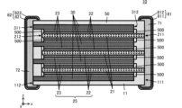
- FIG. 2 is a side cross-sectional view showing the configuration of the solid electrolytic capacitor according to the first embodiment.
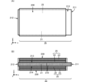
- FIG. 3A is a plan view of the capacitor element, and
- FIG. 3B is a side cross-sectional view of the capacitor element.
- 4(A) and 4(B) are cross-sectional views showing the configuration of the outer layer CP.
- FIG. 5 is a flow chart showing an example of a schematic flow of the method for manufacturing a solid electrolytic capacitor according to this embodiment.
- FIG. 6A is an external perspective view of a capacitor element sheet
- FIG. 6B is an external perspective view of a cathode sheet.
- FIG. 7 is a perspective view showing the appearance of a laminate (sheet-type capacitor laminate) of a capacitor element sheet and a cathode sheet.
- FIG. 8A is a side cross-sectional view showing the configuration of an outer layer CP and a cathode film according to the second embodiment
- FIG. 8B is a side cross-sectional view showing the shape of a recess formed in the cathode film.
- FIG. 1 is an external perspective view of a solid electrolytic capacitor according to an embodiment of the present invention.
- Fig. 2 is a side cross-sectional view showing the configuration of a solid electrolytic capacitor according to an embodiment of the present invention.
- Fig. 2 is a cross-sectional view taken along a plane perpendicular to the top, bottom and end faces of a body of the solid electrolytic capacitor.
- Fig. 2 in order to illustrate the configuration in an easy-to-understand manner, the dimensions in each direction are appropriately emphasized, and in particular, the dimension in the height direction (z-axis direction in the figure) is emphasized.
- the solid electrolytic capacitor 10 includes a base body 11, a resin electrode 71, a resin electrode 72, an external electrode 81, and an external electrode 82.
- Fig. 3A is a plan view of the capacitor element
- Fig. 3B is a side cross-sectional view of the capacitor element
- Fig. 3B is a cross-sectional view taken along a plane perpendicular to the flat film surface and end surface of the capacitor element.
- the capacitor element 20 includes an anode electrode 21, an inner layer CP22, and an outer layer CP23.
- the inner layer CP22 and the outer layer CP23 form a solid electrolyte layer 25.
- the anode electrode 21 is flat and has end faces 211, 212, flat membrane surfaces 213, and flat membrane surfaces 214. Although the detailed structure is omitted in Figures 3(A) and 3(B), the anode electrode 21 has a large number of holes recessed from the flat membrane surfaces 213, 214. In other words, a portion of a certain thickness in the vicinity of the flat membrane surfaces 213, 214 in the anode electrode 21 is a porous body in a porous state. The ratio of the thickness of the porous body and core metal part on one side of the anode electrode 21 to the porous body on the other side is approximately 1:1:1.
- the dielectric layer 210 covers the outer surface of the anode electrode 21.
- the anode electrode 21 is made of, for example, a metal such as aluminum, tantalum, niobium, titanium, zirconium, magnesium, silicon, or an alloy containing these metals.
- the anode electrode 21 is preferably made of aluminum or an aluminum alloy.
- the anode electrode 21 may be a valve metal body (valve metal base) that exhibits so-called valve action.
- the inner layer CP22 covers the surface of the dielectric layer 210.
- the inner layer CP22 is made of a conductive polymer.
- the inner layer CP22 fills the fine recesses in the porous portion.
- the outer layer CP23 covers the surface of the inner layer CP22.
- the outer layer CP23 is a layer formed so as to cover the entire dielectric layer 210 after the inner layer CP22 is formed to fill the fine recesses of the porous portion.
- the outer layer CP23 is made of the same material as the inner layer CP22 and further contains inorganic particles. Note that the outer layer CP23 may be made of a material (including a composition) different from that of the inner layer CP22.
- the inner layer CP22 can be made of polyPEDOT [(3,4-ethylenedioxythiophene):PSS (polystyrene sulfonate)], and the outer layer CP23 can be made of polypyrrole.
- the detailed structure of the outer layer CP23 will be described later.
- the insulator layer 500 is formed near the end faces 211, 212 of the flat membrane surfaces 213, 214 of the anode electrode 21.
- the insulator layer 500 is a frame body, and restricts the formation area of the inner layer CP22 and the outer layer CP23. As a result, for example, the inner layer CP22 and the outer layer CP23 do not reach the end face 211 of the anode electrode 21.
- the anode electrode 21 and the solid electrolyte layer face each other with the dielectric layer 210 in between, and the capacitor element 20 functions as a capacitor with a predetermined capacitance.
- the cathode film 30 is a flat metal film and is made of, for example, aluminum, titanium, copper, silver, or the like.
- the plurality of capacitor elements 20 and the plurality of cathode films 30 are arranged such that their respective flat film surfaces are approximately parallel to the top and bottom surfaces of the element body 11.
- the plurality of capacitor elements 20 and the plurality of cathode films 30 are alternately stacked in a direction perpendicular to the top and bottom surfaces (the height direction of the element body 11 (z-axis direction in the figure)). Note that, although the number of the plurality of capacitor elements 20 is three and the number of the plurality of cathode films 30 is four in Fig. 2, this is not limited thereto.
- the capacitor element 20 and the cathode film 30 adjacent to each other in the stacking direction are in contact with each other. More specifically, the flat film surface of the cathode film 30 is in contact with the outer surface 230 of the outer layer CP23 of the capacitor element 20.
- End faces 211 of the multiple capacitor elements 20 are exposed to the outside of the element body 11 from end face 111 of the element body 11.
- end faces 311 of the multiple cathode films 30 are exposed to the outside of the element body 11 from end face 112 of the element body 11.
- the resin electrode 71 abuts against and covers the end face 111 of the element body 11. In this way, the resin electrode 71 is connected to the end faces 211 of the multiple capacitor elements 20.
- the external electrode 81 has a laminated structure of an electrode film 811 and an electrode film 812.
- the electrode film 811 covers the outer surface of the resin electrode 71.
- the electrode film 812 covers the outer surface of the electrode film 811.
- the resin electrode 71 and the external electrode 81 form a first terminal conductor.
- the resin electrode 72 abuts against and covers the end face 112 of the element body 11. As a result, the resin electrode 72 is connected to the end faces 311 of the multiple cathode films 30.
- the external electrode 82 has a laminated structure of an electrode film 821 and an electrode film 822.
- the electrode film 821 covers the outer surface of the resin electrode 72.
- the electrode film 822 covers the outer surface of the electrode film 821.
- the resin electrode 72 and the external electrode 82 form a second terminal conductor.
- Outer layer CP23 4(A) and 4(B) are cross-sectional views showing the structure of the outer layer CP23.
- the outer layer CP23 shown in FIG. 4(A) and FIG. 4(B) is made of a plurality of conductive polymers (hereinafter, conductive polymer layers 231, 232, 233, 234, and 235).
- conductive polymer layers 231, 232, 233, 234, and 235 are examples of a plurality of conductive polymers.
- the outer layer CP23 is described as being made of a plurality of conductive polymer layers 231, 232, 233, 234, and 235 for the sake of convenience, in reality, the outer layer CP23 is formed of a single layer.
- the dotted lines separating the conductive polymer layers 231, 232, 233, 234, and 235 are imaginary lines showing the distribution of the concentration of inorganic particles contained in the conductive polymer layers. A more detailed structure of the outer layer CP23 will be described later.
- the conductive polymer layers 231-235 include a plurality of inorganic particles 250.
- the material for the inorganic particles 250 for example, silicon (Si) or a metal such as cobalt (Co), chromium (Cr), zinc (Zn), or molybdenum (Mo), an oxide or a complex thereof, or a compound containing them, etc., are preferably used.
- the conductive polymer layer 235 is a layer that contacts the cathode film 30, and the conductive polymer layer 231 is a layer that contacts the inner layer CP22 (see FIG. 4(B)).
- the surface where the conductive polymer layer 231 contacts the inner layer CP22 corresponds to the "contact surface" of the present invention.
- the concentration of the inorganic particles 250 contained in the multiple conductive polymer layers 231-235 changes in stages.
- the concentration of the inorganic particles 250 is lower in the conductive polymer layer 234 than in the conductive polymer layer 235, and is lower in the conductive polymer layer 233 than in the conductive polymer layer 234.
- the concentration of the inorganic particles 250 is lower in the conductive polymer layer 232 than in the conductive polymer layer 233, and is lower in the conductive polymer layer 231 than in the conductive polymer layer 232.
- This structure in which the concentration of the inorganic particles 250 contained in the multiple conductive polymer layers 231-235 changes in stages is realized by applying multiple stages of conductive polymer layers 231-235 with different concentrations of inorganic particles 250.
- the conductive polymer layers 231, 232, 233, 234, and 235 that constitute the outer layer CP23 have a lower concentration of inorganic particles in proportion to the distance from the cathode film 30.
- the inorganic particles 250 are unevenly distributed on the surface of the outer layer CP23 that contacts the cathode film 30.
- the thermal expansion coefficients of the conductive polymer layers 231, 232, 233, 234, and 235 that form the outer layer CP23 are different from the inorganic particles 250 contained in the outer layer CP23. More specifically, the thermal expansion coefficient of the conductive polymer in the outer layer CP23 is high. On the other hand, the thermal expansion coefficient of the inorganic particles 250 in the outer layer CP23 is low. In other words, by heating and pressurizing the solid electrolytic capacitor 10, a difference in thermal expansion occurs between the conductive polymer layers 231, 232, 233, 234, and 235 and the inorganic particles 250. Therefore, different thermal strains occur for each of the conductive polymer layers 231, 232, 233, 234, and 235.
- the concentration of inorganic particles 250 contained inside decreases stepwise (gradually) from conductive polymer layer 235 to conductive polymer layer 231. Therefore, the inside of outer layer CP23 (e.g., conductive polymer layer 233) has a lower concentration of inorganic particles 250 compared to conductive polymer layer 235. Therefore, the inside of outer layer CP23 has high flexibility.
- the structure in which the concentration of inorganic particles 237 inside outer layer CP23 is low acts as a stress relaxation region against deformation due to shear caused by differences in thermal expansion coefficients and increased internal pressure. Therefore, peeling inside solid electrolytic capacitor 10 can be more efficiently suppressed.
- the multiple cathode films 30 are also connected to a resin electrode 72.
- both the cathode films 30 and the resin electrode 72 contain a resin component. This reduces the difference in physical properties between the cathode films 30 and the resin electrode 72, making it possible to suppress peeling and insulation between the cathode films 30 and the resin electrode 72.
- Fig. 5 is a flow chart showing an example of a schematic flow of a method for manufacturing a solid electrolytic capacitor according to this embodiment.
- Fig. 6(A) is an external perspective view of a capacitor element sheet
- Fig. 6(B) is an external perspective view of a cathode sheet.
- Fig. 7 is an external perspective view of a laminate (sheet-type capacitor laminate) of a capacitor element sheet and a cathode sheet.
- the capacitor element sheet 20M is formed (S11). As shown in FIG. 6(A), the capacitor element sheet 20M is a sheet in which a plurality of capacitor elements 20 are arranged two-dimensionally.
- the specific configuration of the plurality of capacitor elements 20 is as described above, and includes an anode electrode 21, a dielectric layer 210, an inner layer CP22, and an outer layer CP23, and an insulator layer 500 is formed for the inner layer CP22 and the outer layer CP23.
- the cathode sheet 30M is formed (S12). As shown in FIG. 6(B), the cathode sheet 30M is a sheet in which a plurality of cathode films 30 are arranged two-dimensionally. The arrangement pitch of the plurality of cathode films 30 is the same as the arrangement pitch of the plurality of capacitor elements 20.
- the multiple capacitor element sheets 20M and the multiple cathode sheets 30M are stacked in order and heated and pressed (S13). More specifically, the multiple capacitor element sheets 20M and the multiple cathode sheets 30M are stacked so that the outer surfaces 230 of the multiple outer layers CP23 of the capacitor element sheets 20M adjacent in the stacking direction face and abut against the cathode film 30 of the cathode sheet 30M. This forms a sheet-type capacitor laminate. Then, heat and pressure are applied to this sheet-type capacitor laminate. This heat and pressure causes the difference in thermal expansion coefficient at the abutting surface between the outer layer CP23 and the cathode film 30 to become gradual and not change suddenly. This suppresses the difference in thermal strain and improves the adhesive strength between the outer layer CP23 and the cathode film 30.
- the sheet-type capacitor laminate is cut along the cutting lines CL1 and CL2 as shown in FIG. 7 to separate the capacitors (S14).
- the cathode sheet 30M cathode film 30
- burrs on the cut surface can be suppressed. This makes it possible to suppress undesirable short circuits, etc.
- the individualized capacitor laminates are covered with insulating resin 50 (S15). At this time, the insulating resin 50 is heated and pressurized. This causes the insulating resin 50 to solidify, and the element body 11 of the solid electrolytic capacitor 10 is formed.
- Terminal conductors are formed on the end faces 111 and 112 of the element body 11 (S16). More specifically, a resin electrode 71 is formed on the end face 111 of the element body 11, and electrode films 811, 812 are formed on the surface of the resin electrode 71. A resin electrode 72 is formed on the end face 112 of the element body 11, and electrode films 821, 822 are formed on the surface of the resin electrode 72.
- the solid electrolytic capacitor 10 can be manufactured without using a conductive adhesive between the outer layer CP 23 and the cathode film 30.
- the solid electrolytic capacitor 10 can be easily and reliably manufactured, with a strong adhesive strength between the outer layer CP 23 and the cathode film 30 and suppressing peeling insulation.
- Fig. 8(A) is a side cross-sectional view showing the configuration of an outer layer CP and a cathode film according to the second embodiment
- Fig. 8(B) is a side cross-sectional view showing the shape of a recess formed in the cathode film.
- the solid electrolytic capacitor 10A according to the second embodiment differs from the solid electrolytic capacitor 10 according to the first embodiment in the structure of the cathode film 30A.
- the other configuration of the solid electrolytic capacitor 10A is the same as that of the solid electrolytic capacitor 10, and a description of similar parts will be omitted.
- the cathode film 30A has recesses 35.
- the recesses 35 are formed on the surface that contacts the outer layer CP23 (conductive polymer layer 235).
- the recesses 35 may be formed in a regular array or in random positions. In other words, the recesses 35 may be formed in positions, sizes, depths (Rz), and numbers that do not impair the function of the cathode film 30A, and are preferably formed evenly on the cathode film 30A.
- At least one inorganic particle 250 is embedded in the recess 35.
- the inorganic particle 250 is unevenly distributed in the cathode film 30A at least to the depth (Rz) of the recess 35.
- the depth of the recess 35 is approximately the thickness Rz of the conductive polymer layer 235.
- This configuration allows the inorganic particles 250 to easily enter the recesses 35. In other words, it is easy to distribute the inorganic particles 250 in large numbers near the joint between the outer layer CP23 and the cathode film 30A, further improving the adhesive strength between the outer layer CP23 and the cathode film 30A.
- Capacitor element 20 (Description of an example of specific materials of each component of solid electrolytic capacitor 10) (Capacitor element)
- the capacitor element 20 is realized, for example, with the following materials and thicknesses.
- the anode electrode 21 is made of, for example, a single metal such as aluminum, tantalum, niobium, titanium, zirconium, magnesium, copper, or an alloy containing these metals.
- the anode electrode 21 is preferably made of aluminum or an aluminum alloy.
- the anode electrode 21 may be any valve action metal that exhibits so-called valve action.
- the anode electrode 21 is preferably flat, and the thickness of the core of the anode electrode 21 (the center part that is not reached by the pores of the porous body) is preferably 5 ⁇ m or more and 100 ⁇ m or less.
- the thickness (thickness of one side) of the porous part (the part where the pores of the porous body are formed) is preferably 5 ⁇ m or more and 200 ⁇ m or less.
- the dielectric layer 210 is preferably made of an oxide film of the anode electrode 21.
- the dielectric layer 210 is formed by oxidizing it in an aqueous solution containing boric acid, phosphoric acid, adipic acid, or their sodium salts, ammonium salts, etc.
- the thickness of the dielectric layer 12 is preferably 1 nm or more and 100 nm or less.
- the inner layer CP22 may be a layer of PEDOT:PSS, which is realized by, for example, a conductive polymer having a skeleton of pyrroles, thiophenes, anilines, etc., or a conductive polymer having a skeleton of thiophenes such as PEDOT [poly(3,4-ethylenedioxythiophene)], which is a conductive polymer having a skeleton of thiophenes, and is composited with polystyrene sulfonic acid (PSS) as a dopant.
- PEDOT poly(3,4-ethylenedioxythiophene)
- the inner layer CP22 is formed, for example, by a method of forming a polymer film of poly(3,4-ethylenedioxythiophene) or the like on the surface of the dielectric layer 210 using a treatment liquid containing a monomer such as 3,4-ethylenedioxythiophene, or a method of applying a dispersion of a polymer such as poly(3,4-ethylenedioxythiophene) to the surface of the dielectric part and drying it.
- the thickness of the outer layer CP23 is preferably 2 ⁇ m or more and 20 ⁇ m or less.
- the material of the outer layer CP23 is the same as the material of the inner layer CP22. As mentioned above, the material of the outer layer CP23 may be different from the material of the inner layer CP22.
- the inner layer CP22 can be formed of PEDOT:PSS, and the outer layer CP23 can be formed of polypyrrole.
- the insulating resin 50 may contain a filler.
- the resin are preferably epoxy resin, phenol resin, polyimide resin, silicone resin, polyamide resin, liquid crystal polymer, etc.
- the filler are preferably insulating oxide particles such as silica particles, alumina particles, titania particles, zirconia particles, etc.
- the maximum diameter of the filler is preferably, for example, 10 ⁇ m or more and 50 ⁇ m or less.
- a material containing silica particles in solid epoxy resin and phenol resin is more preferable.
Landscapes
- Engineering & Computer Science (AREA)
- Power Engineering (AREA)
- Chemical & Material Sciences (AREA)
- Chemical Kinetics & Catalysis (AREA)
- Electrochemistry (AREA)
- Microelectronics & Electronic Packaging (AREA)
- Fixed Capacitors And Capacitor Manufacturing Machines (AREA)
Priority Applications (2)
| Application Number | Priority Date | Filing Date | Title |
|---|---|---|---|
| JP2024565745A JPWO2024135309A1 (https=) | 2022-12-20 | 2023-12-04 | |
| CN202380087692.5A CN120390971A (zh) | 2022-12-20 | 2023-12-04 | 固体电解电容器 |
Applications Claiming Priority (2)
| Application Number | Priority Date | Filing Date | Title |
|---|---|---|---|
| JP2022-203227 | 2022-12-20 | ||
| JP2022203227 | 2022-12-20 |
Publications (1)
| Publication Number | Publication Date |
|---|---|
| WO2024135309A1 true WO2024135309A1 (ja) | 2024-06-27 |
Family
ID=91588292
Family Applications (1)
| Application Number | Title | Priority Date | Filing Date |
|---|---|---|---|
| PCT/JP2023/043228 Ceased WO2024135309A1 (ja) | 2022-12-20 | 2023-12-04 | 固体電解コンデンサ |
Country Status (3)
| Country | Link |
|---|---|
| JP (1) | JPWO2024135309A1 (https=) |
| CN (1) | CN120390971A (https=) |
| WO (1) | WO2024135309A1 (https=) |
Citations (4)
| Publication number | Priority date | Publication date | Assignee | Title |
|---|---|---|---|---|
| JPH08213285A (ja) * | 1994-11-25 | 1996-08-20 | Nec Corp | 固体電解コンデンサ及びその製造方法 |
| WO2014132632A1 (ja) * | 2013-02-28 | 2014-09-04 | 三洋電機株式会社 | 電解コンデンサおよびその製造方法 |
| JP2019087558A (ja) * | 2017-11-01 | 2019-06-06 | パナソニックIpマネジメント株式会社 | 固体電解コンデンサおよびその製造方法 |
| WO2021125045A1 (ja) * | 2019-12-18 | 2021-06-24 | 株式会社村田製作所 | 固体電解コンデンサ |
-
2023
- 2023-12-04 CN CN202380087692.5A patent/CN120390971A/zh active Pending
- 2023-12-04 JP JP2024565745A patent/JPWO2024135309A1/ja active Pending
- 2023-12-04 WO PCT/JP2023/043228 patent/WO2024135309A1/ja not_active Ceased
Patent Citations (4)
| Publication number | Priority date | Publication date | Assignee | Title |
|---|---|---|---|---|
| JPH08213285A (ja) * | 1994-11-25 | 1996-08-20 | Nec Corp | 固体電解コンデンサ及びその製造方法 |
| WO2014132632A1 (ja) * | 2013-02-28 | 2014-09-04 | 三洋電機株式会社 | 電解コンデンサおよびその製造方法 |
| JP2019087558A (ja) * | 2017-11-01 | 2019-06-06 | パナソニックIpマネジメント株式会社 | 固体電解コンデンサおよびその製造方法 |
| WO2021125045A1 (ja) * | 2019-12-18 | 2021-06-24 | 株式会社村田製作所 | 固体電解コンデンサ |
Also Published As
| Publication number | Publication date |
|---|---|
| CN120390971A (zh) | 2025-07-29 |
| JPWO2024135309A1 (https=) | 2024-06-27 |
Similar Documents
| Publication | Publication Date | Title |
|---|---|---|
| US11170941B2 (en) | Solid electrolytic capacitor | |
| US11232912B2 (en) | Solid electrolytic capacitor | |
| CN103430261B (zh) | 固体电解电容器的制造方法以及固体电解电容器 | |
| EP3226270B1 (en) | Solid electrolytic capacitor | |
| JP7259994B2 (ja) | 固体電解コンデンサ | |
| WO2024135309A1 (ja) | 固体電解コンデンサ | |
| CN103531361B (zh) | 固体电解电容器及其制造方法 | |
| JP2018026379A (ja) | 固体電解コンデンサ | |
| WO2019156120A1 (ja) | 電解コンデンサ | |
| JP7419791B2 (ja) | 固体電解コンデンサ | |
| CN115398577B (zh) | 电解电容器以及电解电容器的制造方法 | |
| CN114746968B (zh) | 固体电解电容器 | |
| JP7806906B2 (ja) | 固体電解コンデンサ、および、固体電解コンデンサの製造方法 | |
| CN223155823U (zh) | 固体电解电容器 | |
| JP4671347B2 (ja) | 固体電解コンデンサ | |
| JP7750381B2 (ja) | 固体電解コンデンサの製造方法 | |
| WO2024090047A1 (ja) | 固体電解コンデンサ | |
| JP2025038408A (ja) | 固体電解コンデンサ | |
| JP2007012797A (ja) | 積層型固体電解コンデンサ | |
| WO2025105152A1 (ja) | 固体電解コンデンサ、および固体電解コンデンサの製造方法 | |
| WO2026058571A1 (ja) | 固体電解コンデンサおよび固体電解コンデンサの製造方法 | |
| WO2026083673A1 (ja) | 固体電解コンデンサの製造方法、及び、固体電解コンデンサ | |
| WO2026070017A1 (ja) | 固体電解コンデンサおよび固体電解コンデンサの製造方法 | |
| WO2025164413A1 (ja) | 固体電解コンデンサおよび固体電解コンデンサの接続素子 | |
| WO2024029458A1 (ja) | 固体電解コンデンサ |
Legal Events
| Date | Code | Title | Description |
|---|---|---|---|
| 121 | Ep: the epo has been informed by wipo that ep was designated in this application |
Ref document number: 23906675 Country of ref document: EP Kind code of ref document: A1 |
|
| WWE | Wipo information: entry into national phase |
Ref document number: 2024565745 Country of ref document: JP |
|
| WWE | Wipo information: entry into national phase |
Ref document number: 202380087692.5 Country of ref document: CN |
|
| NENP | Non-entry into the national phase |
Ref country code: DE |
|
| WWP | Wipo information: published in national office |
Ref document number: 202380087692.5 Country of ref document: CN |
|
| 122 | Ep: pct application non-entry in european phase |
Ref document number: 23906675 Country of ref document: EP Kind code of ref document: A1 |