WO2024116615A1 - 被覆工具および切削工具 - Google Patents
被覆工具および切削工具 Download PDFInfo
- Publication number
- WO2024116615A1 WO2024116615A1 PCT/JP2023/037103 JP2023037103W WO2024116615A1 WO 2024116615 A1 WO2024116615 A1 WO 2024116615A1 JP 2023037103 W JP2023037103 W JP 2023037103W WO 2024116615 A1 WO2024116615 A1 WO 2024116615A1
- Authority
- WO
- WIPO (PCT)
- Prior art keywords
- layer
- wear
- grain size
- crystal grains
- average grain
- Prior art date
- Legal status (The legal status is an assumption and is not a legal conclusion. Google has not performed a legal analysis and makes no representation as to the accuracy of the status listed.)
- Ceased
Links
Images



Classifications
-
- C—CHEMISTRY; METALLURGY
- C23—COATING METALLIC MATERIAL; COATING MATERIAL WITH METALLIC MATERIAL; CHEMICAL SURFACE TREATMENT; DIFFUSION TREATMENT OF METALLIC MATERIAL; COATING BY VACUUM EVAPORATION, BY SPUTTERING, BY ION IMPLANTATION OR BY CHEMICAL VAPOUR DEPOSITION, IN GENERAL; INHIBITING CORROSION OF METALLIC MATERIAL OR INCRUSTATION IN GENERAL
- C23C—COATING METALLIC MATERIAL; COATING MATERIAL WITH METALLIC MATERIAL; SURFACE TREATMENT OF METALLIC MATERIAL BY DIFFUSION INTO THE SURFACE, BY CHEMICAL CONVERSION OR SUBSTITUTION; COATING BY VACUUM EVAPORATION, BY SPUTTERING, BY ION IMPLANTATION OR BY CHEMICAL VAPOUR DEPOSITION, IN GENERAL
- C23C30/00—Coating with metallic material characterised only by the composition of the metallic material, i.e. not characterised by the coating process
- C23C30/005—Coating with metallic material characterised only by the composition of the metallic material, i.e. not characterised by the coating process on hard metal substrates
-
- C—CHEMISTRY; METALLURGY
- C23—COATING METALLIC MATERIAL; COATING MATERIAL WITH METALLIC MATERIAL; CHEMICAL SURFACE TREATMENT; DIFFUSION TREATMENT OF METALLIC MATERIAL; COATING BY VACUUM EVAPORATION, BY SPUTTERING, BY ION IMPLANTATION OR BY CHEMICAL VAPOUR DEPOSITION, IN GENERAL; INHIBITING CORROSION OF METALLIC MATERIAL OR INCRUSTATION IN GENERAL
- C23C—COATING METALLIC MATERIAL; COATING MATERIAL WITH METALLIC MATERIAL; SURFACE TREATMENT OF METALLIC MATERIAL BY DIFFUSION INTO THE SURFACE, BY CHEMICAL CONVERSION OR SUBSTITUTION; COATING BY VACUUM EVAPORATION, BY SPUTTERING, BY ION IMPLANTATION OR BY CHEMICAL VAPOUR DEPOSITION, IN GENERAL
- C23C28/00—Coating for obtaining at least two superposed coatings either by methods not provided for in a single one of groups C23C2/00 - C23C26/00 or by combinations of methods provided for in subclasses C23C and C25C or C25D
- C23C28/04—Coating for obtaining at least two superposed coatings either by methods not provided for in a single one of groups C23C2/00 - C23C26/00 or by combinations of methods provided for in subclasses C23C and C25C or C25D only coatings of inorganic non-metallic material
- C23C28/044—Coating for obtaining at least two superposed coatings either by methods not provided for in a single one of groups C23C2/00 - C23C26/00 or by combinations of methods provided for in subclasses C23C and C25C or C25D only coatings of inorganic non-metallic material coatings specially adapted for cutting tools or wear applications
Definitions
- This disclosure relates to coated tools and cutting tools.
- Coated tools are known as tools used in cutting processes such as turning and milling, and have improved wear resistance and other properties by coating the surface of a base material such as cemented carbide, cermet, or ceramics with a coating layer.
- a coated tool includes a substrate and a coating layer located on the substrate.
- the coating layer includes an intermediate layer and a wear-resistant layer located on the intermediate layer.
- the ratio of the average grain size of the crystal grains that make up the wear-resistant layer to the average grain size of the crystal grains that make up the intermediate layer is 0.7 or less.
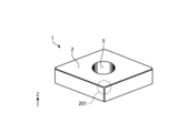
- FIG. 1 is a perspective view showing an example of a coated tool according to an embodiment.
- FIG. 2 is a side cross-sectional view showing an example of a coated tool according to an embodiment.
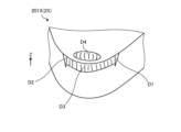
- FIG. 3 is a schematic enlarged view of a corner portion of a chip body according to a reference example.
- FIG. 4 is a cross-sectional view illustrating an example of a coating layer according to an embodiment.
- FIG. 5 is a front view illustrating an example of a cutting tool according to an embodiment.
- FIG. 6 is a graph showing the correlation between cutting time and abrasive wear amount.
- FIG. 7 is an image showing the cutting edge state of the coated tool according to the example after the cutting test.
- FIG. 8 is an image showing the cutting edge state of the coated tool according to the comparative example after the cutting test.
- Coated tools are known as tools used in cutting processes such as turning and milling, and have improved wear resistance and other properties by coating the surface of a base material such as cemented carbide, cermet, or ceramics with a coating layer.
- Fig. 1 is a perspective view showing an example of a coated tool according to an embodiment.
- Fig. 2 is a side cross-sectional view showing an example of a coated tool according to an embodiment.
- a coated tool 1 according to an embodiment has a tip body 2.
- Chip body 2 has, for example, a hexahedral shape with the upper and lower surfaces (surfaces intersecting with the Z-axis shown in FIG. 1) each being a parallelogram.
- the cutting edge portion has a first surface (e.g., a top surface) and a second surface (e.g., a side surface) that is connected to the first surface.
- the first surface functions as a "scooping surface” that scoops up chips generated by cutting
- the second surface functions as a "flank surface.”
- a cutting edge is located on at least a portion of the ridge where the first surface and the second surface intersect, and the coated tool 1 cuts the workpiece by applying this cutting edge to the workpiece.
- a through hole 5 that passes through the chip body 2 from top to bottom is located in the center of the chip body 2.
- a screw 75 is inserted into the through hole 5 to attach the coated tool 1 to a holder 70 (described later) (see FIG. 5).
- the shape of the coated tool 1 shown in FIG. 1 is merely an example and does not limit the shape of the coated tool according to the present disclosure.
- the coated tool according to the present disclosure may have, for example, a rod-shaped body having a rotation axis and extending from a first end to a second end, a cutting edge located at the first end of the body, and a groove extending in a spiral shape from the cutting edge toward the second end of the body.
- the chip body 2 has a base 10 and a coating layer 20.
- the substrate 10 is formed of, for example, a cemented carbide.
- the cemented carbide contains a hard phase containing at least W (tungsten), specifically WC (tungsten carbide).
- the cemented carbide may contain a binder phase containing at least one iron group element such as Ni (nickel) or Co (cobalt).
- the substrate 10 is made of a WC-based cemented carbide having hard particles made of WC as a hard phase component and Co as a main component of the binder phase.
- the substrate 10 has better heat resistance properties.
- the substrate 10 may be formed of a cermet.
- the cermet contains, for example, Ti (titanium), specifically, TiC (titanium carbide) or TiN (titanium nitride).
- Ti titanium
- TiC titanium carbide
- TiN titanium nitride
- the cermet may also contain Ni or Co.
- the substrate 10 may be formed of a cubic boron nitride sintered body containing cubic boron nitride (cBN) particles.
- the substrate 10 is not limited to cubic boron nitride (cBN) particles, and may contain particles of hexagonal boron nitride (hBN), rhombohedral boron nitride (rBN), wurtzite boron nitride (wBN), or the like.
- the substrate 10 may be made of ceramics.
- the ceramics may contain, for example, aluminum oxide (Al 2 O 3 ), such as ⁇ -Al 2 O 3 and ⁇ -Al 2 O 3.
- the ceramics may contain other elements in addition to aluminum oxide.
- the ceramics may contain at least one of magnesium (Mg), calcium (Ca), strontium (Sr), silicon (Si), and a Group 3 element of the periodic table, in addition to aluminum oxide.
- the coating layer 20 coats the substrate 10 for the purpose of improving the wear resistance, heat resistance, etc. of the substrate 10.
- the coating layer 20 coats the substrate 10 as a whole.
- the arrangement of the coating layer 20 on the substrate 10 is not particularly limited as long as the coating layer 20 is located at least on the surface of the substrate 10.
- the coating layer 20 is located on the first surface (here, the upper surface) of the substrate 10, the wear resistance and heat resistance of the first surface are high.
- the coating layer 20 is located on the second surface (here, the side surface) of the substrate 10, the wear resistance and heat resistance of the second surface are high.
- Fig. 3 is a schematic enlarged view of a corner portion 201X of a chip body 2X according to a reference example.
- the chip body 2X may undergo wear such as primary boundary wear D1, secondary boundary wear D2, abrasive wear D3, and crater wear D4.
- Primary boundary wear D1, secondary boundary wear D2, and abrasive wear D3 are wear that occurs on the flank face, and crater wear D4 is wear that occurs on the rake face.
- Abrasive wear D3 is a wear phenomenon in which the surface of the tip body 2X is scraped off by foreign matter interposed between the tip body 2X and the workpiece. Abrasive wear D3 may cause an increase in cutting resistance and cutting heat.
- Primary boundary wear D1 and secondary boundary wear D2 are wear that occurs at both ends of abrasive wear D3, i.e., at the cut boundaries.
- the primary boundary is the boundary that comes into contact with the cutting surface of the workpiece
- the secondary boundary is the boundary that comes into contact with the finished surface of the workpiece.
- Primary boundary wear D1 may cause burrs to form in the workpiece.
- Secondary boundary wear D2 may deteriorate the finished surface of the workpiece or change the dimensions of the workpiece.
- Crater wear D4 occurs when the tip body 2X becomes hot and the surface is oxidized, producing relatively soft oxides. Crater wear D4 may cause chip disposal to deteriorate.
- the coated tool 1 according to the embodiment can effectively reduce these damages by devising a structure for the coating layer 20 that covers the tip body 2.
- Fig. 4 is a cross-sectional view showing an example of the covering layer 20 according to the embodiment.
- the coating layer 20 has an adhesion layer 21, an intermediate layer 22, and an abrasion-resistant layer 23.
- the adhesion layer 21 is a layer that contacts the substrate 10.
- the intermediate layer 22 is located on the surface of the adhesion layer 21.
- the abrasion-resistant layer 23 is located on the surface of the intermediate layer 22. That is, the adhesion layer 21, the intermediate layer 22, and the abrasion-resistant layer 23 are laminated in this order from the surface side of the substrate 10: adhesion layer 21, intermediate layer 22, and abrasion-resistant layer 23.
- the adhesion layer 21 is an alloy layer containing Ti a Al b M c .
- M is at least one metal selected from Groups 4a, 5a, and 6a of the periodic table, and Si.
- the adhesion layer 21 may be TiAlWNbSi.
- the adhesion layer 21 does not necessarily need to contain M.
- the adhesion layer 21 may be, for example, TiAl.
- the adhesion layer 21 improves the adhesion of the coating layer 20 to the substrate 10. As a result, the adhesion layer 21 can reduce the occurrence of primary boundary wear D1 and secondary boundary wear D2 in the chip body 2.
- Intermediate layer 22 includes Ti d Al e M f and at least one nonmetal selected from carbon, nitrogen, and oxygen.
- M is at least one metal selected from Groups 4a, 5a, and 6a of the periodic table (excluding Cr), and Si.
- intermediate layer 22 may be TiAlWNbSiN.
- the intermediate layer 22 does not necessarily contain M.
- the intermediate layer 22 may be, for example, TiAlN.
- the intermediate layer 22 has high oxidation resistance. As a result, the intermediate layer 22 can reduce the occurrence of crater wear D4 in the chip body 2.
- the wear-resistant layer 23 includes Ti g Al h Cr i M j and at least one nonmetal selected from carbon, nitrogen, and oxygen.
- M is at least one metal selected from Groups 4a, 5a, and 6a of the periodic table (excluding Cr) and Si.
- the wear-resistant layer 23 may be TiAlCrWNbSiN.
- the wear-resistant layer 23 does not necessarily need to contain M.
- the wear-resistant layer 23 may be, for example, TiAlCrN.
- the wear-resistant layer 23 is a layer that comes into contact with the workpiece when the workpiece is cut with the coated tool 1, and can reduce the occurrence of primary boundary wear D1, secondary boundary wear D2, and abrasive wear D3 in the tip body 2.
- the adhesion layer 21, the intermediate layer 22, and the wear-resistant layer 23 may each have Ti and Al as their main components.
- the term "main component” means that the content ratio in atomic percent is higher than that of other components.
- Ti and Al are contained as the main components, high wear resistance and high defect resistance can be exhibited.
- the intermediate layer 22 and the wear-resistant layer 23 each contain Ti and Al as their main components, the thermal expansion difference between the adhesion layer 21, the intermediate layer 22, and the wear-resistant layer 23 can be kept small. Therefore, cracks are less likely to occur at the interface between the adhesion layer 21 and the intermediate layer 22, and at the interface between the intermediate layer 22 and the wear-resistant layer 23.
- Mc in the adhesion layer 21, Mf in the intermediate layer 22, and Mj in the wear-resistant layer 23 do not need to be limited to a specific metal element, and do not need to be limited to a specific content.
- the proportion of metal components in the adhesion layer 21, intermediate layer 22, and wear-resistant layer 23 can be determined, for example, by analysis using an EDS (energy dispersive X-ray spectrometer) attached to a STEM (scanning transmission electron microscope).
- EDS energy dispersive X-ray spectrometer
- STEM scanning transmission electron microscope
- the thickness of the coating layer 20 may be 2.5 ⁇ m or more and 10 ⁇ m or less.
- wear resistance particularly resistance to abrasive wear D3
- chipping of the coating layer 20 can be more easily reduced. Therefore, when the thickness of the coating layer 20 is 2.5 ⁇ m or more and 10 ⁇ m or less, the wear resistance and chipping resistance of the coating layer 20 can be improved.
- the thickness of the adhesion layer 21 may be 2 nm or more and 8 nm or less.
- the adhesion of the coating layer 20 to the substrate 10 can be more easily improved.
- the occurrence of primary boundary wear D1 and secondary boundary wear D2 in the chip body 2 can be more easily reduced.
- the thickness of the adhesion layer 21 is 8 nm or less, the destruction of the coating layer 20 can be more easily reduced by reducing the plastic deformation of the relatively soft adhesion layer 21. Therefore, when the thickness of the adhesion layer 21 is 2 nm or more and 8 nm or less, the occurrence of primary boundary wear D1 and secondary boundary wear D2 in the chip body 2 and the destruction of the coating layer 20 can be reduced.
- the thickness of the intermediate layer 22 may be less than the thickness of the wear-resistant layer 23.
- the thickness of the intermediate layer 22 may be 0.5 ⁇ m or more and 3 ⁇ m or less.
- the thickness of the intermediate layer 22 is 0.5 ⁇ m or more, the occurrence of crater wear D4 in the chip body 2 can be more easily reduced.
- the thickness of the intermediate layer 22 is 3 ⁇ m or less, the effect of the wear-resistant layer 23 in reducing the occurrence of primary boundary wear D1, secondary boundary wear D2, and abrasive wear D3 in the chip body 2 can be more easily ensured. Therefore, when the thickness of the intermediate layer 22 is 0.5 ⁇ m or more and 3 ⁇ m or less, damage to the chip body 2 can be more easily reduced.
- the thickness of the wear-resistant layer 23 may be 1.5 ⁇ m or more and 7 ⁇ m or less.
- the thickness of the wear-resistant layer 23 is 1.5 ⁇ m or more, the occurrence of primary boundary wear D1, secondary boundary wear D2, and abrasive wear D3 in the chip body 2 can be more easily reduced.
- the thickness of the intermediate layer 22 is 7 ⁇ m or less, the effect of the intermediate layer 22 in reducing the occurrence of crater wear D4 in the chip body 2 can be more easily ensured. Therefore, when the thickness of the wear-resistant layer 23 is 1.5 ⁇ m or more and 7 ⁇ m or less, damage to the chip body 2 can be more easily reduced.
- the coating layer 20 is composed of the adhesion layer 21, the intermediate layer 22, and the wear-resistant layer 23, but the coating layer 20 does not necessarily need to include the adhesion layer 21.
- the coated tool 1 may have a coating layer 20 composed of the intermediate layer 22 located on the surface of the substrate 10 and the wear-resistant layer 23 located on the surface of the intermediate layer 22.
- the ratio of the average grain size W23 of the crystal grains constituting the wear-resistant layer 23 to the average grain size W22 of the crystal grains constituting the intermediate layer 22 is 0.7 or less.
- the ratio of the average grain size W23 of the crystal grains constituting the wear-resistant layer 23 to the average grain size W22 of the crystal grains constituting the intermediate layer 22 is, for example, 0.5 or less, and may be 0.15 or less.
- the average grain size W22 of the crystal grains constituting the intermediate layer 22 and the average grain size W23 of the crystal grains constituting the wear-resistant layer 23 can be obtained, for example, as follows. First, a photograph of the cross section of the coating layer 20 including the intermediate layer 22 and the wear-resistant layer 23 in a direction perpendicular to the surface of the substrate 10 is taken using a scanning transmission electron microscope (STEM) or the like. Next, the maximum and minimum grain sizes are obtained for each of a predetermined number of crystal grains constituting the intermediate layer 22 or the wear-resistant layer 23 in the cross section of the coating layer 20. Here, particles with a maximum diameter of less than 3 nm are excluded from the evaluation because it is difficult to evaluate whether they are crystal grains or not.
- STEM scanning transmission electron microscope
- the average value of the maximum and minimum diameters of the crystal grains is calculated as the grain size of the crystal grains.
- the average value of the grain sizes for a predetermined number of crystal grains is calculated as the average grain size of the crystal grains.
- the predetermined number is, for example, a number that allows the average grain size of the crystal grains to be determined with approximately three significant digits.
- the average grain size W23 of the crystal grains constituting the wear-resistant layer 23 can be relatively reduced. This can reduce the occurrence of cracks in the wear-resistant layer 23.
- the average grain size W22 of the crystal grains constituting the intermediate layer 22 can be relatively increased. This can reduce the progression of cracks in the intermediate layer 22.
- both the average grain size W22 of the crystal grains constituting the intermediate layer 22 and the average grain size W23 of the crystal grains constituting the wear-resistant layer 23 are small, it is possible to reduce the occurrence of cracks in the wear-resistant layer 23, but it may be difficult to reduce the progression of cracks in the intermediate layer 22. If both the average grain size W22 of the crystal grains constituting the intermediate layer 22 and the average grain size W23 of the crystal grains constituting the wear-resistant layer 23 are large, it is possible to reduce the progression of cracks in the intermediate layer 22, but it may be difficult to reduce the occurrence of cracks in the wear-resistant layer 23.
- the ratio of the average grain size W23 of the crystal grains constituting the wear-resistant layer 23 to the average grain size W22 of the crystal grains constituting the intermediate layer 22 is 0.7 or less, it is possible to reduce both the occurrence of cracks in the wear-resistant layer 23 and the progression of cracks in the intermediate layer 22. This makes it possible to improve the wear resistance of the coated tool 1. For example, it is possible to improve the wear resistance of the coated tool 1 in machining a heat-resistant alloy. As a result, it is possible to extend the tool life of the coated tool 1.
- the ratio of the average grain size W23 of the crystal grains constituting the wear-resistant layer 23 to the average grain size W22 of the crystal grains constituting the intermediate layer 22 may be 0.05 or more.
- the relative increase in the average grain size W22 of the crystal grains constituting the intermediate layer 22 to the average grain size W23 of the crystal grains constituting the wear-resistant layer 23 can be reduced. Therefore, the occurrence of cracks in the intermediate layer 22 can be reduced. This can further improve the wear resistance of the coated tool 1.
- the average grain size W22 of the crystal grains constituting the intermediate layer 22 may be 100 nm or less. In this case, the occurrence of cracks in the intermediate layer 22 can be reduced. This can further improve the wear resistance of the coated tool 1.
- the average grain size W22 of the crystal grains constituting the intermediate layer 22 may be 70 nm or less. In this case, the occurrence of cracks in the intermediate layer 22 can further be reduced.
- the average grain size W23 of the crystal grains forming the wear-resistant layer 23 may be 70 nm or less. In this case, the occurrence of cracks in the wear-resistant layer 23 can be further reduced. This can further improve the wear resistance of the coated tool 1.
- the average grain size W23 of the crystal grains forming the wear-resistant layer 23 may be 50 nm or less. In this case, the occurrence of cracks in the wear-resistant layer 23 can be further reduced.
- the average grain size W23 of the crystal grains forming the wear-resistant layer 23 may be 10 nm or less. In this case, the occurrence of cracks in the wear-resistant layer 23 can be further reduced.
- coating layer (first layer) 20A the one located at the corner portion 201 of the chip body 2 is referred to as coating layer (first layer) 20A
- coating layer (second layer) 20B the one located on the first surface (rake face) of the chip body 2
- coating layer (third layer) 20C the one located on the second surface (flank face) of the chip body 2.
- the average grain size of the crystal grains in these coating layers 20A, 20B, and 20C will be described below.
- the average grain size of the crystal grains in coating layer 20A may be evaluated at a location located on the ridge where the first and second surfaces intersect.
- the average grain size of the crystal grains in coating layer 20B may be evaluated at a location on the first surface that is 500 ⁇ m away from the ridge.
- the average grain size of the crystal grains in coating layer 20C may be evaluated at a location on the second surface that is 500 ⁇ m away from the ridge.
- the ratio of the average grain size W23A, W23B, and W23C of the crystal grains constituting the wear-resistant layer 23 to the average grain size W22A, W22B, and W22C of the crystal grains constituting the intermediate layer 22 may be 0.7 or less.
- the values of W23A/W22A, W23B/W22B, and W23C/W22C may each be 0.7 or less. In this case, the wear resistance of the cutting edge, rake face, and flank face is improved.
- W23A/W22A, W23B/W22B and W23C/W22C may be the same value or may be different from each other.
- W23A/W22A may be greater than W23B/W22B and W23C/W22C.
- the ratio of W23A/W22A to W23B/W22B and W23C/W22C may be 1.05 or greater.
- Coating layer 20B located on the rake face and coating layer 20C located on the flank face are required to have high wear resistance.
- W23B/W22B and W23C/W22C are relatively small, high wear resistance can be achieved on the rake face and flank face.
- coating layer 20A located on the cutting edge is required to have high chipping resistance in addition to wear resistance.
- W23A/W22A is relatively large, high chipping resistance can be ensured at the cutting edge. Therefore, the coated tool 1 as a whole can exhibit high durability.
- W23B/W22B and W23C/W22C may be the same value or may be different from each other.
- W23B/W22B may be smaller than W23C/W22C.
- the ratio of W23B/W22B to W23C/W22C may be 0.95 or less.
- the rake face with which the chips come into contact is more susceptible to wear than the flank face.
- W23C/W22C may be smaller than W23B/W22B.
- the ratio of W23C/W22C to W23B/W22B may be 0.95 or less.
- the average grain size W23A in coating layer 20A may be larger than the average grain size W23B in coating layer 20B and the average grain size W23C in coating layer 20C.
- the ratio of W23A to W23B and W23C may be 1.1 or more.
- the average grain size W22A in coating layer 20A may be larger than the average grain size W22B in coating layer 20B and the average grain size W22C in coating layer 20C.
- the ratio of W22A to W22B and W22C may be 1.05 or more.
- W22A is relatively large, high chipping resistance can be ensured at the cutting edge. Therefore, the coated tool 1 as a whole can exhibit high durability.
- the ratio of W23A to W23B and W23C may be larger than the ratio of W22A to W22B and W22C.
- Method of manufacturing the coating layer 20 Next, an example of a method for producing the coating layer 20 according to the present embodiment will be described.
- the method for producing the coating layer 20 according to the present embodiment is not limited to the following method.
- the coating layer 20 may be formed, for example, by a physical vapor deposition (PVD) method.
- PVD physical vapor deposition
- the coating layer 20 can be formed so as to cover the entire surface of the substrate 10 except for the inner circumferential surface of the through hole 5.
- Examples of physical vapor deposition include ion plating such as arc ion plating (AIP) and sputtering.
- Arc ion plating is a method of forming a film of metal or metal nitride by evaporating a target metal using arc discharge in a vacuum atmosphere and combining it with N2 gas or the like as necessary.
- the bias voltage applied to the substrate 10, which is the object to be coated may be -30V or less.
- the coating layer 20 when the coating layer 20 is produced by the arc ion plating method, the coating layer 20 can be produced by the following method.
- metal targets of Ti, Al, and M (wherein M is at least one metal selected from Groups 4a, 5a, and 6a of the periodic table, and Si), composite alloy targets, or sintered compact targets are prepared.
- the above target which is the metal source
- the above target which is the metal source
- the above target is evaporated and ionized by arc discharge or glow discharge, and the ionized metal is deposited on the surface of the substrate 10.
- the adhesion layer 21 can be formed.
- the composition of the adhesion layer 21 can be adjusted by controlling the voltage or current value during arc discharge or glow discharge applied to each of the various metal targets independently for each target.
- the composition of the adhesion layer 21 can also be adjusted by controlling the composition of the metal target, the coating time, or the atmospheric gas pressure.
- the thickness of the adhesion layer 21 can be adjusted, for example, by controlling the coating time.
- metal targets of Ti, Al, and M (where M is at least one metal selected from Groups 4a, 5a, and 6a of the periodic table (excluding Cr), and Si), composite alloy targets, or sintered targets are prepared.
- the target which is the metal source
- the target is evaporated and ionized by arc discharge, glow discharge, or the like.
- the ionized metal is reacted with nitrogen (N 2 ) gas or the like and evaporated onto the surface of the substrate 10.
- N 2 nitrogen
- the composition of the intermediate layer 22 can be adjusted by controlling the composition of the metal target.
- the grain size of the intermediate layer 22 can be adjusted by controlling the current value during arc discharge or glow discharge, or by controlling the atmospheric gas pressure.
- the thickness of the intermediate layer 22 can be adjusted, for example, by controlling the coating time.
- a method for manufacturing the wear-resistant layer 23 will be described.
- a metal target of Ti, Al, Cr, or M (where M is at least one metal selected from Groups 4a, 5a, and 6a of the periodic table (excluding Cr), and Si), a composite alloy target, or a sintered target is prepared.
- the target which is the metal source
- the target which is the metal source
- the ionized metal is reacted with nitrogen (N 2 ) gas or the like and is evaporated onto the surface of the substrate 10.
- the abrasion-resistant layer 23 can be formed by the above procedure.
- the composition of the wear-resistant layer 23 can be adjusted by controlling the composition of the metal target.
- the grain size of the wear-resistant layer 23 can be adjusted by controlling the voltage or current value during arc discharge or glow discharge, or by controlling the atmospheric gas pressure.
- the thickness of the wear-resistant layer 23 can be adjusted, for example, by controlling the coating time.
- Fig. 5 is a front view showing an example of a cutting tool according to an embodiment.
- the cutting tool 100 has a coated tool 1 and a holder 70 for fixing the coated tool 1.
- the holder 70 is a rod-shaped member that extends from a first end (the upper end in FIG. 5) to a second end (the lower end in FIG. 5).
- the holder 70 is made of, for example, steel or cast iron. Of these materials, steel, which has particularly high toughness, may be used.
- the holder 70 has a pocket 73 at the end on the first end side.
- the pocket 73 is the portion where the coated tool 1 is attached, and has a seating surface that intersects with the rotation direction of the workpiece and a restraining side surface that is inclined relative to the seating surface.
- the seating surface has a screw hole into which a screw 75, which will be described later, is screwed.
- the coated tool 1 is located in the pocket 73 of the holder 70 and is attached to the holder 70 by a screw 75. That is, the screw 75 is inserted into the through hole 5 of the coated tool 1, and the tip of the screw 75 is inserted into a screw hole formed in the seating surface of the pocket 73 to screw the threaded portions together. In this way, the coated tool 1 is attached to the holder 70 so that the cutting edge portion protrudes outward from the holder 70.
- a cutting tool 100 used for so-called turning is exemplified.
- Examples of turning include internal diameter machining, external diameter machining, and grooving.
- the cutting tool is not limited to that used for turning.
- the coated tool 1 may be used as a cutting tool used for turning.
- Examples of cutting tools used for turning include milling cutters such as flat milling cutters, face milling cutters, side milling cutters, and groove milling cutters, and end mills such as single-blade end mills, multiple-blade end mills, tapered-blade end mills, and ball end mills.
- a coated tool including a substrate and a coating layer consisting of an adhesion layer, an intermediate layer, and an abrasion-resistant layer was produced as an example by sequentially laminating an adhesion layer, an intermediate layer, and an abrasion-resistant layer on the substrate by an arc ion plating method.
- a WC-based cemented carbide was used as the substrate.
- the compositions and thicknesses of the adhesion layer, intermediate layer, and abrasion-resistant layer formed on the substrate are shown in Table 1.
- the maximum diameter, minimum diameter, and grain size of the crystal grains that make up the intermediate layer are shown in Table 2.
- the maximum diameter, minimum diameter, and grain size of the crystal grains that make up the wear-resistant layer, and the ratio of the average grain size of the crystal grains that make up the wear-resistant layer to the average grain size of the crystal grains that make up the intermediate layer are shown in Table 2.
- the grain size, maximum diameter, and minimum diameter of the crystal grains that make up the intermediate layer and wear-resistant layer can be measured as follows.
- the grain size of the crystal grains can be determined by determining the area of each crystal grain and approximating it to a circle to determine the grain size.
- the grain size of the crystal grains can be determined by using OIM Analysis made by TSL.
- the crystal grains are approximated as ellipses, and the long and short diameters of the ellipses are determined.
- the long and short diameters are set as the maximum and minimum diameters of the crystal grains, and the average grain size of the crystal grains can be determined by averaging the maximum and minimum diameters.
- the maximum and minimum diameters of the crystal grains constituting the intermediate layer and the maximum and minimum diameters of the crystal grains constituting the wear-resistant layer were measured for the cutting edge of a conventional coated tool as a comparative example.
- the grain sizes of the crystal grains constituting the intermediate layer and the wear-resistant layer were calculated.
- the ratio of the average grain size of the crystal grains constituting the wear-resistant layer to the average grain size of the crystal grains constituting the intermediate layer was calculated. The results are shown in Table 2.
- the maximum diameter, minimum diameter, and grain size of the crystal grains that make up the intermediate layer and the wear-resistant layer were measured, and the ratio of the average grain size of the crystal grains that make up the wear-resistant layer to the average grain size of the crystal grains that make up the intermediate layer was calculated.
- the grain size was measured under the above conditions.
- the time until the abrasive wear amount reached 0.2 mm was measured from the images obtained by photographing the abrasive wear of each sample after the cutting test was performed under the following conditions, and the time until the abrasive wear amount reached 0.2 mm was calculated.
- the ratio of the average grain size of the crystal grains constituting the wear-resistant layer to the average grain size of the crystal grains constituting the intermediate layer was 0.7 or less for both the cutting edge and side of the coated tool according to the embodiment.
- the ratio of the average grain size of the crystal grains constituting the wear-resistant layer to the average grain size of the crystal grains constituting the intermediate layer was greater than 0.7 for the cutting edge of the coated tool according to the comparative example.
- Cutting tests were conducted on the coated tools according to the examples and the comparative examples.
- the cutting test conditions were as follows:
- abrasive wear amount the length of abrasive wear in the thickness direction of the coating layer of the coated tool according to the embodiment. The cutting times in the cutting test were 7.4 minutes, 14.8 minutes, 19.8 minutes, 24.7 minutes, 29.7 minutes, and 34.6 minutes.
- the amount of abrasive wear in the thickness direction of the coating layer of the coated tool according to the comparative example shown in sample No. 8 was measured.
- the cutting times in the cutting test were 7.4 minutes and 14.8 minutes.
- FIG. 6 is a graph showing the correlation between cutting time and abrasive wear amount.
- the horizontal axis of the graph shown in FIG. 6 is cutting time (minutes).
- the vertical axis of the graph shown in FIG. 6 is abrasive wear amount (mm).
- white circles indicate measured values for the coated tool of the embodiment.
- Black circles indicate measured values for the coated tool of the comparative example.
- the wear resistance of the coated tool can be improved. In other words, it was confirmed that the tool life of the coated tool can be extended.
- Figure 7 is an image showing the cutting edge condition after a cutting test of the coated tool according to the embodiment.
- Figure 8 is an image showing the cutting edge condition after a cutting test of the coated tool according to the comparative example.
- the part of the cutting edge of the coated tool where the coating layer has been scraped off by abrasive wear D3 and the substrate has been exposed is shown by a dotted white circle.
- a substrate; a coating layer overlying the substrate; Equipped with the coating layer includes an intermediate layer and an abrasion-resistant layer located on the intermediate layer, The ratio of the average grain size of the crystal grains constituting the wear-resistant layer to the average grain size of the crystal grains constituting the intermediate layer is 0.7 or less.
- the average grain size of the crystal grains constituting the intermediate layer is 100 nm or less, The average grain size of the crystal grains constituting the wear-resistant layer is 70 nm or less. 13.
- the average grain size of the crystal grains constituting the intermediate layer is 70 nm or less, The average grain size of the crystal grains constituting the wear-resistant layer is 50 nm or less.
- the coating layer further includes an adhesion layer in contact with the substrate. A coated tool according to any one of appendices (1) to (3).
- the intermediate layer, the wear-resistant layer and the adhesion layer are each mainly composed of Ti and Al. The coated tool according to claim 4.
- the substrate is a first surface that functions as a rake surface; a second surface acting as a clearance surface; a ridge line located at an intersection of the first surface and the second surface;
- the coating layer is A first layer located on the ridge line; a second layer overlying the first surface; and a third layer overlying the second surface; the ratio in the first layer is greater than the ratio in the second layer and the third layer;
- the ratio in the second layer is greater than the ratio in the third layer; The coated tool according to claim 6.
- the ratio in the third layer is greater than the ratio in the second layer; The coated tool according to claim 6.
- the average grain size of the crystal grains constituting the wear-resistant layer in the first layer is larger than the average grain size of the crystal grains constituting the wear-resistant layer in the second layer and the third layer; A coated tool according to any one of appendices (6) to (8).
- the average grain size of the crystal grains constituting the intermediate layer in the first layer is larger than the average grain size of the crystal grains constituting the intermediate layer in the second layer and the third layer; A coated tool according to any one of appendices (6) to (9).
Landscapes
- Chemical & Material Sciences (AREA)
- Chemical Kinetics & Catalysis (AREA)
- Engineering & Computer Science (AREA)
- Materials Engineering (AREA)
- Mechanical Engineering (AREA)
- Metallurgy (AREA)
- Organic Chemistry (AREA)
- Inorganic Chemistry (AREA)
- Cutting Tools, Boring Holders, And Turrets (AREA)
Priority Applications (3)
| Application Number | Priority Date | Filing Date | Title |
|---|---|---|---|
| JP2024561222A JPWO2024116615A1 (https=) | 2022-11-30 | 2023-10-12 | |
| DE112023004976.9T DE112023004976T5 (de) | 2022-11-30 | 2023-10-12 | Beschichtetes werkzeug und schneidwerkzeug |
| CN202380078252.3A CN120112379A (zh) | 2022-11-30 | 2023-10-12 | 涂层刀具以及切削刀具 |
Applications Claiming Priority (2)
| Application Number | Priority Date | Filing Date | Title |
|---|---|---|---|
| JP2022192382 | 2022-11-30 | ||
| JP2022-192382 | 2022-11-30 |
Publications (1)
| Publication Number | Publication Date |
|---|---|
| WO2024116615A1 true WO2024116615A1 (ja) | 2024-06-06 |
Family
ID=91323638
Family Applications (1)
| Application Number | Title | Priority Date | Filing Date |
|---|---|---|---|
| PCT/JP2023/037103 Ceased WO2024116615A1 (ja) | 2022-11-30 | 2023-10-12 | 被覆工具および切削工具 |
Country Status (4)
| Country | Link |
|---|---|
| JP (1) | JPWO2024116615A1 (https=) |
| CN (1) | CN120112379A (https=) |
| DE (1) | DE112023004976T5 (https=) |
| WO (1) | WO2024116615A1 (https=) |
Citations (4)
| Publication number | Priority date | Publication date | Assignee | Title |
|---|---|---|---|---|
| JP2018164974A (ja) * | 2017-03-28 | 2018-10-25 | 株式会社タンガロイ | 被覆切削工具 |
| JP2019155537A (ja) * | 2018-03-14 | 2019-09-19 | 三菱マテリアル株式会社 | 表面被覆切削工具 |
| WO2021241021A1 (ja) * | 2020-05-26 | 2021-12-02 | 住友電気工業株式会社 | 切削工具 |
| JP2022030402A (ja) * | 2020-08-07 | 2022-02-18 | 三菱マテリアル株式会社 | 表面被覆切削工具 |
-
2023
- 2023-10-12 DE DE112023004976.9T patent/DE112023004976T5/de active Pending
- 2023-10-12 CN CN202380078252.3A patent/CN120112379A/zh active Pending
- 2023-10-12 WO PCT/JP2023/037103 patent/WO2024116615A1/ja not_active Ceased
- 2023-10-12 JP JP2024561222A patent/JPWO2024116615A1/ja active Pending
Patent Citations (4)
| Publication number | Priority date | Publication date | Assignee | Title |
|---|---|---|---|---|
| JP2018164974A (ja) * | 2017-03-28 | 2018-10-25 | 株式会社タンガロイ | 被覆切削工具 |
| JP2019155537A (ja) * | 2018-03-14 | 2019-09-19 | 三菱マテリアル株式会社 | 表面被覆切削工具 |
| WO2021241021A1 (ja) * | 2020-05-26 | 2021-12-02 | 住友電気工業株式会社 | 切削工具 |
| JP2022030402A (ja) * | 2020-08-07 | 2022-02-18 | 三菱マテリアル株式会社 | 表面被覆切削工具 |
Also Published As
| Publication number | Publication date |
|---|---|
| JPWO2024116615A1 (https=) | 2024-06-06 |
| CN120112379A (zh) | 2025-06-06 |
| DE112023004976T5 (de) | 2025-09-11 |
Similar Documents
| Publication | Publication Date | Title |
|---|---|---|
| KR101635488B1 (ko) | 절삭 공구 | |
| JP5406041B2 (ja) | 多層被覆切削工具 | |
| CN103052456B (zh) | 被覆工具 | |
| KR101685450B1 (ko) | 절삭 공구 | |
| JP4714022B2 (ja) | 工具用表面被覆高硬度材料 | |
| KR101758691B1 (ko) | 절삭 공구 | |
| EP3527309A1 (en) | Surface-coated cutting tool | |
| JP4745243B2 (ja) | 耐摩耗層 | |
| CN114040991A (zh) | 制造涂布的切削工具的方法和涂布的切削工具 | |
| WO2024116615A1 (ja) | 被覆工具および切削工具 | |
| JP7638381B2 (ja) | 被覆工具および切削工具 | |
| JP7600405B2 (ja) | 被覆工具および切削工具 | |
| WO2024225321A1 (ja) | 被覆工具および切削工具 | |
| JP7422862B2 (ja) | 被覆工具および切削工具 | |
| WO2023243007A1 (ja) | 切削工具 | |
| WO2024185718A1 (ja) | 被覆工具および切削工具 | |
| JP7764578B2 (ja) | 被覆工具および切削工具 | |
| JP7806210B2 (ja) | 被覆工具および切削工具 | |
| JP7646009B2 (ja) | 被覆工具および切削工具 | |
| WO2026018875A1 (ja) | 被覆工具、切削工具、および切削加工物の製造方法 | |
| JP7795453B2 (ja) | 被覆工具および切削工具 | |
| WO2025164764A1 (ja) | 被覆工具および切削工具 | |
| JP7621497B2 (ja) | 被覆工具および切削工具 | |
| JP7607777B2 (ja) | 被覆工具および切削工具 | |
| JP4895586B2 (ja) | 表面被覆切削工具 |
Legal Events
| Date | Code | Title | Description |
|---|---|---|---|
| 121 | Ep: the epo has been informed by wipo that ep was designated in this application |
Ref document number: 23897273 Country of ref document: EP Kind code of ref document: A1 |
|
| WWE | Wipo information: entry into national phase |
Ref document number: 2024561222 Country of ref document: JP |
|
| WWE | Wipo information: entry into national phase |
Ref document number: 202380078252.3 Country of ref document: CN |
|
| WWP | Wipo information: published in national office |
Ref document number: 202380078252.3 Country of ref document: CN |
|
| WWE | Wipo information: entry into national phase |
Ref document number: 112023004976 Country of ref document: DE |
|
| WWP | Wipo information: published in national office |
Ref document number: 112023004976 Country of ref document: DE |
|
| 122 | Ep: pct application non-entry in european phase |
Ref document number: 23897273 Country of ref document: EP Kind code of ref document: A1 |