WO2024111510A1 - 電子部品 - Google Patents
電子部品 Download PDFInfo
- Publication number
- WO2024111510A1 WO2024111510A1 PCT/JP2023/041407 JP2023041407W WO2024111510A1 WO 2024111510 A1 WO2024111510 A1 WO 2024111510A1 JP 2023041407 W JP2023041407 W JP 2023041407W WO 2024111510 A1 WO2024111510 A1 WO 2024111510A1
- Authority
- WO
- WIPO (PCT)
- Prior art keywords
- layer
- insulating layer
- electrode pattern
- electronic component
- conductor
- Prior art date
- Legal status (The legal status is an assumption and is not a legal conclusion. Google has not performed a legal analysis and makes no representation as to the accuracy of the status listed.)
- Ceased
Links
Images




Classifications
-
- H—ELECTRICITY
- H01—ELECTRIC ELEMENTS
- H01F—MAGNETS; INDUCTANCES; TRANSFORMERS; SELECTION OF MATERIALS FOR THEIR MAGNETIC PROPERTIES
- H01F17/00—Fixed inductances of the signal type
-
- H—ELECTRICITY
- H01—ELECTRIC ELEMENTS
- H01F—MAGNETS; INDUCTANCES; TRANSFORMERS; SELECTION OF MATERIALS FOR THEIR MAGNETIC PROPERTIES
- H01F27/00—Details of transformers or inductances, in general
-
- H—ELECTRICITY
- H01—ELECTRIC ELEMENTS
- H01F—MAGNETS; INDUCTANCES; TRANSFORMERS; SELECTION OF MATERIALS FOR THEIR MAGNETIC PROPERTIES
- H01F27/00—Details of transformers or inductances, in general
- H01F27/28—Coils; Windings; Conductive connections
- H01F27/32—Insulating of coils, windings, or parts thereof
-
- H—ELECTRICITY
- H01—ELECTRIC ELEMENTS
- H01G—CAPACITORS; CAPACITORS, RECTIFIERS, DETECTORS, SWITCHING DEVICES, LIGHT-SENSITIVE OR TEMPERATURE-SENSITIVE DEVICES OF THE ELECTROLYTIC TYPE
- H01G4/00—Fixed capacitors; Processes of their manufacture
- H01G4/30—Stacked capacitors
-
- H—ELECTRICITY
- H01—ELECTRIC ELEMENTS
- H01G—CAPACITORS; CAPACITORS, RECTIFIERS, DETECTORS, SWITCHING DEVICES, LIGHT-SENSITIVE OR TEMPERATURE-SENSITIVE DEVICES OF THE ELECTROLYTIC TYPE
- H01G4/00—Fixed capacitors; Processes of their manufacture
- H01G4/33—Thin- or thick-film capacitors (thin- or thick-film circuits; capacitors without a potential-jump or surface barrier specially adapted for integrated circuits, details thereof, multistep manufacturing processes therefor)
-
- H—ELECTRICITY
- H01—ELECTRIC ELEMENTS
- H01G—CAPACITORS; CAPACITORS, RECTIFIERS, DETECTORS, SWITCHING DEVICES, LIGHT-SENSITIVE OR TEMPERATURE-SENSITIVE DEVICES OF THE ELECTROLYTIC TYPE
- H01G4/00—Fixed capacitors; Processes of their manufacture
- H01G4/40—Structural combinations of fixed capacitors with other electric elements, the structure mainly consisting of a capacitor, e.g. RC combinations
Definitions
- This disclosure relates to electronic components, and in particular to electronic components having a capacitor disposed on a substrate.
- Patent document 1 discloses a surface-mounted chip-type electronic component that includes a capacitor mounted on a substrate.
- This disclosure describes technology that can provide electronic components with highly reliable capacitors.
- An electronic component includes a substrate, a first insulating layer covering a surface of the substrate, an adhesion layer provided on the surface of the first insulating layer and extending to surround at least a partial region of the first insulating layer, a lower electrode pattern provided in a first region of the first insulating layer, which is a region surrounded by the adhesion layer, a second insulating layer provided in the first region to cover the lower electrode pattern, an upper electrode pattern covering the lower electrode pattern via the second insulating layer, and an interlayer insulating film provided on the first insulating layer and embedding the adhesion layer, the lower electrode pattern, the second insulating layer, and the upper electrode pattern, and an edge of the second insulating layer is located on the adhesion layer.
- the technology disclosed herein provides an electronic component having a highly reliable capacitor.
- FIG. 1 is a schematic perspective view showing the appearance of an electronic component 100 according to an embodiment of the technology disclosed herein.
- FIG. 2 is a schematic cross-sectional view of the electronic component 100.
- FIG. 3 is an equivalent circuit diagram of the electronic component 100.
- FIG. 4 is a schematic plan view showing the pattern shapes of the conductor layers M1 and MM.
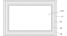
- FIG. 5 is a schematic plan view illustrating an example of the pattern shape of the adhesive layer 13.
- FIG. 6 is a schematic plan view illustrating another example of the pattern shape of the adhesive layer 13.
- FIG. 7 is a schematic plan view showing an example in which eight slits SL1 to SL8 are provided in the adhesive layer 13. As shown in FIG. FIG. FIG.
- FIG. 8 is a schematic plan view showing the pattern shape of the conductor layer M2.
- FIG. 9 is a schematic plan view showing the pattern shape of the conductor layer M3.
- FIG. 10 is a schematic plan view showing the pattern shape of the conductor layers M4 and M5.
- FIG. 11 is a schematic cross-sectional view taken along line AA of FIG.
- FIG. 1 is a simplified perspective view showing the appearance of an electronic component 100 according to one embodiment of the technology disclosed herein.
- FIG. 2 is a simplified cross-sectional view of the electronic component 100.
- the electronic component 100 is a surface-mounted high-pass filter, and as shown in FIG. 1, includes a substrate 10, an interlayer insulating film 20 formed on the surface of the substrate 10, and signal terminals S1, S2 and ground terminals G1, G2 formed on the surface of the interlayer insulating film 20.
- the surface of the substrate 10 is covered with an insulating layer 11 provided for planarization and the like, and a plurality of conductor layers M1 to M4, MM covered with an interlayer insulating film 20 are provided on the insulating layer 11.
- the conductor layers M1 to M4, MM are made of good conductors such as copper (Cu).
- the signal terminals S1, S2 and the ground terminals G1, G2 are formed on the conductor layer M5 located on the top layer.
- the interlayer insulating film 20 includes four interlayer insulating films 21 to 24.
- an organic insulating material such as polyimide resin, epoxy resin, or benzocyclobutene resin may be used as the material for the interlayer insulating film 20.
- the material of the substrate 10 may be any material that is chemically and thermally stable, generates little stress, and can maintain a smooth surface. However, it is not particularly limited, and examples of the material that can be used include silicon single crystal, alumina, sapphire, aluminum nitride, MgO single crystal, SrTiO3 single crystal, surface silicon oxide, glass, quartz, and ferrite.
- the material of the insulating layer 11 may be an inorganic insulating material such as alumina ( Al2O3 ), silicon nitride ( Si3N4 ), and silicon oxide ( SiO2 ). When the insulating layer 11 is made of an inorganic insulating material, the adhesion with the interlayer insulating film 21 made of an organic insulating material may be insufficient, and in this case, peeling is likely to occur at the interface between the two.
- FIG. 3 is an equivalent circuit diagram of the electronic component 100 according to this embodiment.
- the electronic component 100 has capacitors C1, C2, C4, and C5 connected in series between signal terminals S1 and S2, a capacitor C3 connected in parallel to capacitors C1 and C2, a capacitor C6 connected in parallel to capacitors C4 and C5, an inductor L1 connected between the connection point of capacitors C1 and C2 and ground terminals G1 and G2, and an inductor L2 connected between the connection point of capacitors C4 and C5 and ground terminals G1 and G2.
- the electronic component 100 according to this embodiment functions as a high-pass filter.
- the frequency characteristics of the high-pass filter are basically determined by the capacitance of capacitors C1 to C6 and the inductance of inductors L1 and L2.
- the conductor layer M1 is the bottommost conductor layer, and includes conductor patterns 31-34, winding patterns 35, 36, lower electrode patterns 37, 38, and dummy pattern 39, as shown in FIG. 4.
- the conductor patterns 31-34 are provided at positions overlapping with the signal terminals S1, S2 and the ground terminals G1, G2, respectively, in a plan view.
- the winding patterns 35, 36 are patterns that rotate for about one turn, and each constitute a part of the inductors L1, L2.
- the lower electrode patterns 37, 38 are provided between the conductor patterns 31 and 32. Of these, the lower electrode pattern 37 is connected to the conductor pattern 31, and the lower electrode pattern 38 is connected to the conductor pattern 32.
- the dummy pattern 39 is provided between the conductor patterns 33 and 34, and is not connected to any conductor pattern.
- the conductor patterns 31-34 and the winding patterns 35, 36 are connected to the upper conductor layer M2 via via holes 31a-36a provided in the interlayer insulating film 21, respectively.
- the surface of the conductor layer M1 is covered with an insulating layer 12 which is a capacitive insulating film of the capacitor, and the conductor layer MM is provided on the insulating layer 12.
- the insulating layer 12 may be made of an inorganic insulating material such as silicon nitride (Si 3 N 4 ) or silicon oxide (SiO 2 ).
- Si 3 N 4 silicon nitride
- SiO 2 silicon oxide
- the conductor layer MM includes upper electrode patterns 41 to 46.
- the upper electrode patterns 41 and 42 are provided at a position overlapping a portion of the winding pattern 35, and the upper electrode patterns 44 and 45 are provided at a position overlapping a portion of the winding pattern 36.
- the upper electrode pattern 41 is provided at a position overlapping one end of the winding pattern 35, and the upper electrode pattern 45 is provided at a position overlapping one end of the winding pattern 36.
- the upper electrode pattern 42 is provided at a position close to the other end of the winding pattern 35, and the upper electrode pattern 44 is provided at a position close to the other end of the winding pattern 36.
- the portions of the winding patterns 35 and 36 that overlap the upper electrode patterns 41, 42, 44, and 45 function as lower electrodes.
- the winding pattern 35, the upper electrode pattern 41, and the insulating layer 12 form a capacitor C1
- the winding pattern 35, the upper electrode pattern 42, and the insulating layer 12 form a capacitor C2.
- the winding pattern 36, the upper electrode pattern 44, and the insulating layer 12 form a capacitor C4
- the winding pattern 36, the upper electrode pattern 45, and the insulating layer 12 form a capacitor C5.
- the upper electrode patterns 43 and 46 are also provided at positions overlapping the lower electrode patterns 37 and 38, respectively.
- the lower electrode pattern 37, the upper electrode pattern 43, and the insulating layer 12 form a capacitor C3
- the lower electrode pattern 38, the upper electrode pattern 46, and the insulating layer 12 form a capacitor C6.
- the upper electrode patterns 41 to 46 are connected to the upper conductor layer M2 through via holes 41a to 46a provided in the interlayer insulating film 21, respectively.
- an adhesion layer 13 is provided between insulating layer 11 and insulating layer 12.
- Adhesion layer 13 is made of a highly adhesive metal material such as chromium (Cr), titanium (Ti), tantalum (Ta), aluminum (Al), nickel (Ni), or an alloy containing any of these, or an oxide or nitride of any of these, and serves to prevent peeling at the interface between insulating layer 11 and insulating layer 12 by being interposed therebetween. These materials are characterized by high adhesion to inorganic insulating materials and organic insulating materials compared to copper (Cu) constituting conductor layers M1 to M5 and MM.
- Cu copper
- the adhesive layer 13 is provided on the surface of the insulating layer 11 and extends to surround at least a portion of the insulating layer 11 (hereinafter, sometimes referred to as the first region).
- the adhesive layer 13 extends in a ring shape along the outer periphery of the insulating layer 11, and a central region 11A (first region) surrounded by the adhesive layer 13 is formed.
- Each conductor pattern included in the conductor layers M1 to M5, MM is disposed on the central region 11A of the insulating layer 11 in a plan view.
- the insulating layer 12 is formed so that its edge overlaps the adhesive layer 13.
- the edge portion of the insulating layer 12 is not in direct contact with the insulating layer 11, and the adhesive layer 13 is interposed between them.
- the position of the edge of the insulating layer 12 may be closer to the inner edge of the adhesive layer 13 than to the outer edge of the adhesive layer 13, as shown in FIG. 5.
- the adhesion layer 13 may have a continuous ring-shaped structure as shown in FIG. 5, or an intermittent ring-shaped structure as shown in FIG. 6. In other words, it is sufficient that the adhesion layer 13 extends along the outer periphery of the insulating layer 11 so as to surround the central region 11A of the insulating layer 11.
- the number of slits formed in the adhesion layer 13 is not particularly limited, and may be, for example, 2, 4, 8, 16, or more.
- FIG. 7 is a schematic plan view showing an example in which eight slits SL1 to SL8 are provided in the adhesive layer 13.
- the adhesion layer 13 is divided into eight segments 131 to 138 by slits SL1 to SL8.
- the outer periphery of the insulating layer 11 has sides 111 and 112 extending in the X direction, sides 113 and 114 extending in the Y direction, a corner 115 where the sides 111 and 113 terminate, a corner 116 where the sides 111 and 114 terminate, a corner 117 where the sides 112 and 113 terminate, and a corner 118 where the sides 112 and 114 terminate.
- Segment 131 extends in the X direction along side 111 of the insulating layer 11
- segment 132 extends in the X direction along side 112 of the insulating layer 11
- segment 133 extends in the Y direction along side 113 of the insulating layer 11
- segment 134 extends in the Y direction along side 114 of the insulating layer 11.
- Segment 135 extends in an L-shape along side 111, corner 115, and side 113 of insulating layer 11.
- Segment 136 extends in an L-shape along side 111, corner 116, and side 114 of insulating layer 11.
- Segment 137 extends in an L-shape along side 112, corner 117, and side 113 of insulating layer 11.
- Segment 138 extends in an L-shape along side 112, corner 118, and side 114 of insulating layer 11.
- Slit SL1 separates segments 131 and 135.
- Slit SL2 separates segments 131 and 136.
- Slit SL3 separates segments 132 and 137.
- Slit SL4 separates segments 132 and 138.
- Slit SL5 separates segments 133 and 135.
- Slit SL6 separates segments 133 and 137.
- Slit SL7 separates segments 134 and 136.
- Slit SL8 separates segments 134 and 138.
- Slits SL1 and SL2 are provided at positions along side 111 of insulating layer 11.
- Slits SL3 and SL4 are provided at positions along side 112 of insulating layer 11.
- Slits SL3 and SL4 are provided at positions along side 113 of insulating layer 11.
- Slits SL7 and SL8 are provided at positions along side 114 of insulating layer 11.
- the conductor pattern 31 connected to the signal terminal S1 overlaps with the segment 135 from the X and Y directions.
- the conductor pattern 32 connected to the signal terminal S2 overlaps with the segment 136 from the X and Y directions.
- the conductor pattern 33 connected to the ground terminal G1 overlaps with the segment 137 from the X and Y directions.
- the conductor pattern 34 connected to the ground terminal G2 overlaps with the segment 138 from the X and Y directions.
- the positions of slits SL1 to SL4 in the X direction overlap with conductor patterns 31 to 34, respectively.
- the positions of slits SL5 and SL6 in the Y direction overlap with winding pattern 35.
- the positions of slits SL7 and SL8 in the Y direction overlap with winding pattern 36.
- the slits SL1 to SL8 By providing such slits SL1 to SL8 in the adhesive layer 13, unintended propagation paths of high frequency signals through stray capacitances occurring between each of the segments 131 to 138 and the conductor patterns 31 to 34, the winding patterns 35, 36, the lower electrode patterns 37, 38, and the dummy pattern 39 located on the conductor layer M1 are cut off.
- the slits SL1 and SL2 cut off the propagation path through the adhesive layer 13 formed between the conductor pattern 31 connected to the signal terminal S1 and the conductor pattern 32 connected to the signal terminal S2.
- the slit SL3 cuts off the propagation path through the adhesive layer 13 formed between the conductor pattern 33 connected to the ground terminal G1 and the dummy pattern 39.
- the slit SL4 cuts off the propagation path through the adhesive layer 13 formed between the conductor pattern 34 connected to the ground terminal G2 and the dummy pattern 39.
- the slit SL5 separates the propagation path through the adhesive layer 13 formed between the conductor pattern 31 connected to the signal terminal S1 and the winding pattern 35.
- the slit SL6 separates the propagation path through the adhesive layer 13 formed between the conductor pattern 33 connected to the ground terminal G1 and the winding pattern 35.
- the slit SL7 separates the propagation path through the adhesive layer 13 formed between the conductor pattern 32 connected to the signal terminal S2 and the winding pattern 36.
- the slit SL8 separates the propagation path through the adhesive layer 13 formed between the conductor pattern 34 connected to the ground terminal G2 and the winding pattern 36.
- the adhesive layer 13 is divided into eight segments 131-138 by the slits SL1-SL8, so that bonding between adjacent patterns in the conductor layer M1 via the adhesive layer 13 is suppressed.
- conductor patterns 31-34 are present at positions adjacent to the slits SL1-SL4 in the Y direction
- a winding pattern 35 is present at a position adjacent to the slits SL5 and SL6 in the X direction
- a winding pattern 36 is present at a position adjacent to the slits SL7 and SL8 in the X direction.
- the width of the slits SL1-SL8 may be equal to or less than the width of the adhesive layer 13.
- the structure of the adhesion layer 13 shown in FIG. 7 is merely one example, and various modifications are possible.
- two slits are provided along each of the sides 111-114 of the insulating layer 11, but the number of slits provided along each of the sides 111-114 may be one, or may be three or more.
- the number of slits provided along the long sides 111 and 112 may be greater than the number of slits provided along the short sides 113 and 114.
- the adhesion layer 13 may be provided on the surface of the conductor layer M1 as shown in FIG. 2, rather than only on the portion extending in an annular shape along the outer periphery of the insulating layer 11. This makes it less likely that peeling will occur between the lower electrode pattern formed by the conductor layer M1 and the insulating layer 12.
- the adhesion layer 13 is made of a conductive material, the adhesion layer 13 is not formed over the entire surface of the central region 11A of the insulating layer 11, but is divided for each pattern that constitutes the conductor layer M1.
- the adhesion layer 13 is made of a conductive material, the portion extending along the outer periphery of the insulating layer 11 may be in a floating state without being connected to any conductor pattern.
- the adhesion layer 13 may be formed at any time after the insulating layer 11 is formed and before the insulating layer 12 is formed, but if the adhesion layer 13 is also provided on the surface of the conductor layer M1, the adhesion layer 13 is formed after the conductor layer M1 is formed and before the insulating layer 12 is formed.
- the insulating layer 11, conductor layer M1, adhesion layer 13, insulating layer 12, and conductor layer MM are embedded in the interlayer insulating film 21.
- the conductor layer M2 is located above the conductor layer M1 via the interlayer insulating film 21, and includes conductor patterns 50-54, 57, connection patterns 58, 59, and winding patterns 55, 56, as shown in FIG. 8.
- the conductor patterns 51-54 are connected to the conductor patterns 31-34 of the conductor layer M1 via via holes 31a-34a provided in the interlayer insulating film 21, respectively.
- the winding patterns 55, 56 are patterns that rotate for about one turn, and each constitutes a part of the inductors L1, L2.
- One end of the winding patterns 55, 56 is connected to the other end of the winding patterns 35, 36 of the conductor layer M1 via via holes 35a, 36a provided in the interlayer insulating film 21, respectively.
- the conductor pattern 57 is commonly connected to the upper electrode patterns 42, 43, 44, 46 of the conductor layer M1 via via holes 42a, 43a, 44a, 46a provided in the interlayer insulating film 21.
- the connection pattern 58 is a pattern that protrudes from the conductor pattern 51 toward the winding pattern 55, is connected to the conductor pattern 51 in the plane, and is connected to the upper electrode pattern 41 of the conductor layer M1 through a via hole 41a provided in the interlayer insulating film 21.
- connection pattern 59 is a pattern that protrudes from the conductor pattern 52 toward the winding pattern 56, is connected to the conductor pattern 52 in the plane, and is connected to the upper electrode pattern 45 of the conductor layer M1 through a via hole 45a provided in the interlayer insulating film 21.
- the conductor pattern 50 is a pattern that connects the conductor pattern 53 and the conductor pattern 54, and plays a role in shorting the ground terminals G1 and G2.
- a dummy pattern 39 is present at a position that overlaps with the conductor pattern 50, thereby ensuring flatness.
- the conductor patterns 51 to 54 and the winding patterns 55 and 56 are connected to the upper conductor layer M3 through via holes 51a to 56a provided in the interlayer insulating film 22, respectively.
- the conductor layer M3 is located above the conductor layer M2 via the interlayer insulating film 22, and includes conductor patterns 61-64 and winding patterns 65, 66 as shown in FIG. 9.
- the conductor patterns 61-64 are connected to the conductor patterns 51-54 of the conductor layer M2 via via holes 51a-54a provided in the interlayer insulating film 22, respectively.
- the winding patterns 65, 66 are patterns that rotate for about 0.5 turns, and each constitutes a part of the inductors L1, L2.
- One end of the winding patterns 65, 66 is connected to the other end of the winding patterns 55, 56 of the conductor layer M2 via via holes 55a, 56a provided in the interlayer insulating film 22, respectively.
- winding patterns 65, 66 are connected to the conductor patterns 63, 64, respectively.
- the conductor patterns 61-64 are connected to the upper conductor layer M4 via via holes 61a-64a provided in the interlayer insulating film 23, respectively.
- the conductor layer M4 is located above the conductor layer M3 via the interlayer insulating film 23, and includes conductor patterns 71 to 74 as shown in FIG. 10.
- the conductor patterns 71 to 74 are connected to the conductor patterns 61 to 64 of the conductor layer M3 via via holes 61a to 64a provided in the interlayer insulating film 23, respectively, and are connected to the upper conductor layer M5 via via holes 71a to 74a provided in the interlayer insulating film 24, respectively.
- the conductor layer M5 includes signal terminals S1, S2 and ground terminals G1, G2.
- the signal terminals S1, S2 and the ground terminals G1, G2 are connected to the conductor patterns 71 to 74 of the conductor layer M4 via via holes 71a to 74a provided in the interlayer insulating film 24, respectively.
- the above-mentioned conductor layers M1 to M5, MM are all made of a good conductor such as Cu (copper).
- the surfaces of the signal terminals S1, S2 and the ground terminals G1, G2 may be subjected to a surface treatment to enhance wettability with solder.
- inductor L1 is formed by winding patterns 35, 55, 65, and 75
- inductor L2 is formed by winding patterns 36, 56, 66, and 76.
- the winding directions of inductors L1 and L2 starting from ground terminals G1 and G2 are opposite to each other, so that current flows in the same direction in adjacent sections of inductors L1 and L2 on the same conductor layer.
- FIG. 11 is a schematic cross-sectional view taken along line A-A in FIG. 4.
- the adhesive layer 13 extends in a ring shape along the outer periphery of the insulating layer 11 so as to surround the central region 11A of the insulating layer 11.
- the insulating layer 12, which functions as a capacitive insulating film, is formed so that its edge overlaps with the adhesive layer 13, so that peeling is less likely to occur at the edge of the insulating layer 12.
- the insulating layer 11 and the interlayer insulating film 21 have low adhesion, and peeling B may occur from the outer periphery at the interface between the two.
- the position of the edge of the insulating layer 12 is not particularly limited as long as it overlaps with the adhesive layer 13, but if it is closer to the inner edge of the adhesive layer 13 than to the outer edge of the adhesive layer 13, that is, if it is set inside the center position in the width direction of the adhesive layer 13, the effect of stopping the progression of peeling is enhanced. Furthermore, in this embodiment, since the adhesive layer 13 is also provided on the surface of the conductor layer M1, it is also possible to prevent peeling between the lower electrode pattern formed by the conductor layer M1 and the insulating layer 12.
- the adhesion layer 13 may be formed to surround a generally central region on the surface of the insulating layer 11, as in the embodiment described above, or may be formed to surround another region (e.g., a specific region offset in any direction when viewed from above).
- the shape of the adhesion layer 13 may be formed in a generally straight line along the outer edge of the insulating layer 11, as in the embodiment described above, or may have bent portions, inflected portions, meandering portions, etc. formed in some parts.
- An electronic component includes a substrate, a first insulating layer covering the surface of the substrate, an adhesive layer provided on the surface of the first insulating layer and extending to surround at least a portion of the first insulating layer, a lower electrode pattern provided in the first region of the first insulating layer, which is the region surrounded by the adhesive layer, a second insulating layer provided in the first region to cover the lower electrode pattern, an upper electrode pattern covering the lower electrode pattern via the second insulating layer, and an interlayer insulating film provided on the first insulating layer and embedding the adhesive layer, the lower electrode pattern, the second insulating layer, and the upper electrode pattern, and the edge of the second insulating layer is located on the adhesive layer.
- the peeling of the interlayer insulating film stops at the edge portion of the second insulating layer, so that cracks and the like are less likely to occur in the second insulating layer that functions as a capacitive insulating film. This improves the reliability of the components of the capacitor, thereby realizing an electronic component having a highly reliable capacitor.
- the adhesion layer may be formed at the outer edge of the first insulating layer so as to extend along the periphery of the first insulating layer and surround the first region. This can effectively prevent the first insulating layer from peeling away from the outer edge.
- the edge of the second insulating layer may be located closer to the inner edge of the adhesive layer than to the outer edge of the adhesive layer. This makes it possible to more effectively stop the progression of peeling.
- the first insulating layer and the second insulating layer may be made of different inorganic insulating materials
- the adhesion layer may be made of a conductive material different from the lower electrode pattern and the upper electrode pattern
- the interlayer insulating film may be made of an organic insulating material. This makes it possible to suppress peeling between the different materials by the adhesion layer.
- the adhesion layer may contain Cr, Ti, Ta, Al, or Ni. This makes it possible to ensure high adhesion to inorganic insulating materials and organic insulating materials.
- the first insulating layer may contain Al 2 O 3 , Si 3 N 4 or SiO 2. This makes it possible to ensure sufficient surface smoothness.
- the second insulating layer may contain Si 3 N 4 or SiO 2. This makes it possible to obtain a sufficient capacitance.
- the interlayer insulating film may contain polyimide resin, epoxy resin, or benzocyclobutene resin. This makes it possible to obtain high embedding characteristics.
- one or more slits may be provided in the adhesive layer. This makes it possible to suppress unintended signal propagation through the adhesive layer.
- the electronic component further includes a plurality of terminal electrodes arranged at positions overlapping the first region in a plan view, the periphery of the first insulating layer has a first side, the plurality of terminal electrodes include first and second terminal electrodes arranged along the first side in a plan view, the adhesion layer includes a first segment provided along the first side and adjacent to the first terminal electrode, and a second segment provided along the first side and adjacent to the second terminal electrode, and the slit may separate the first segment and the second segment. This makes it possible to suppress unintended bonding of the first terminal electrode and the second terminal electrode via the adhesion layer.
- the adhesion layer may include a plurality of segments adjacent to the plurality of terminal electrodes, and the slits may separate the plurality of segments from one another. This makes it possible to suppress unintended bonding between the plurality of terminal electrodes via the adhesion layer.
- the lower electrode pattern is formed on a first conductor layer, and a plurality of conductor patterns including the lower electrode pattern are formed on the first conductor layer, and the slit may be disposed in a position adjacent to the plurality of conductor patterns. This makes it possible to suppress the occurrence of peeling caused by the slit.
- the interlayer insulating film includes a first interlayer insulating film that embeds the adhesion layer, the lower electrode pattern, the second insulating layer, and the upper electrode pattern, and one or more second interlayer insulating layers laminated on the first interlayer insulating film, and the multiple terminal electrodes may be provided on the outermost layer of the second interlayer insulating film. This makes it possible to provide a surface-mount electronic component that includes multiple conductor layers.
Landscapes
- Engineering & Computer Science (AREA)
- Power Engineering (AREA)
- Microelectronics & Electronic Packaging (AREA)
- Manufacturing & Machinery (AREA)
- Coils Or Transformers For Communication (AREA)
Priority Applications (1)
| Application Number | Priority Date | Filing Date | Title |
|---|---|---|---|
| JP2024560117A JPWO2024111510A1 (https=) | 2022-11-25 | 2023-11-17 |
Applications Claiming Priority (2)
| Application Number | Priority Date | Filing Date | Title |
|---|---|---|---|
| JP2022-187845 | 2022-11-25 | ||
| JP2022187845 | 2022-11-25 |
Publications (1)
| Publication Number | Publication Date |
|---|---|
| WO2024111510A1 true WO2024111510A1 (ja) | 2024-05-30 |
Family
ID=91195667
Family Applications (1)
| Application Number | Title | Priority Date | Filing Date |
|---|---|---|---|
| PCT/JP2023/041407 Ceased WO2024111510A1 (ja) | 2022-11-25 | 2023-11-17 | 電子部品 |
Country Status (2)
| Country | Link |
|---|---|
| JP (1) | JPWO2024111510A1 (https=) |
| WO (1) | WO2024111510A1 (https=) |
Citations (2)
| Publication number | Priority date | Publication date | Assignee | Title |
|---|---|---|---|---|
| WO2020121801A1 (ja) * | 2018-12-11 | 2020-06-18 | 株式会社村田製作所 | 樹脂多層基板、および樹脂多層基板の製造方法 |
| WO2020230414A1 (ja) * | 2019-05-13 | 2020-11-19 | 株式会社村田製作所 | キャパシタ |
-
2023
- 2023-11-17 WO PCT/JP2023/041407 patent/WO2024111510A1/ja not_active Ceased
- 2023-11-17 JP JP2024560117A patent/JPWO2024111510A1/ja active Pending
Patent Citations (2)
| Publication number | Priority date | Publication date | Assignee | Title |
|---|---|---|---|---|
| WO2020121801A1 (ja) * | 2018-12-11 | 2020-06-18 | 株式会社村田製作所 | 樹脂多層基板、および樹脂多層基板の製造方法 |
| WO2020230414A1 (ja) * | 2019-05-13 | 2020-11-19 | 株式会社村田製作所 | キャパシタ |
Also Published As
| Publication number | Publication date |
|---|---|
| JPWO2024111510A1 (https=) | 2024-05-30 |
Similar Documents
| Publication | Publication Date | Title |
|---|---|---|
| US11170930B2 (en) | Inductor component | |
| JP5206775B2 (ja) | 電子部品 | |
| JP5195876B2 (ja) | コイル部品及びその製造方法 | |
| JP5488566B2 (ja) | コモンモードフィルタ | |
| JP7473437B2 (ja) | 電子部品 | |
| CN204045316U (zh) | 共模扼流圈及高频电子器件 | |
| JP2013038392A (ja) | 電子部品及びその製造方法 | |
| US12513993B2 (en) | Chip-type electronic component | |
| JP6520801B2 (ja) | 電子部品 | |
| JP6819499B2 (ja) | コイル部品およびその製造方法 | |
| WO2015178136A1 (ja) | コイル部品およびこのコイル部品を備えるモジュール | |
| JP2005317725A (ja) | 電子部品 | |
| WO2024111510A1 (ja) | 電子部品 | |
| JP4684856B2 (ja) | 電子部品 | |
| JP2022139098A (ja) | インダクタ部品および電子部品 | |
| JP6841370B2 (ja) | コイル部品 | |
| JP2005116647A (ja) | コモンモードチョークコイル及びその製造方法並びにコモンモードチョークコイルアレイ | |
| WO2024111251A1 (ja) | 電子部品 | |
| US20250149218A1 (en) | Inductor component | |
| JP2024024991A (ja) | 電子部品 | |
| JP2022131768A (ja) | 電子部品 | |
| JP7776023B2 (ja) | 集積化受動部品 | |
| JP7435528B2 (ja) | インダクタ部品 | |
| JP4501077B2 (ja) | 薄膜デバイス | |
| WO2024034205A1 (ja) | 電子部品 |
Legal Events
| Date | Code | Title | Description |
|---|---|---|---|
| 121 | Ep: the epo has been informed by wipo that ep was designated in this application |
Ref document number: 23894519 Country of ref document: EP Kind code of ref document: A1 |
|
| WWE | Wipo information: entry into national phase |
Ref document number: 2024560117 Country of ref document: JP |
|
| NENP | Non-entry into the national phase |
Ref country code: DE |
|
| 122 | Ep: pct application non-entry in european phase |
Ref document number: 23894519 Country of ref document: EP Kind code of ref document: A1 |