WO2024106370A1 - Rfidモジュール - Google Patents
Rfidモジュール Download PDFInfo
- Publication number
- WO2024106370A1 WO2024106370A1 PCT/JP2023/040716 JP2023040716W WO2024106370A1 WO 2024106370 A1 WO2024106370 A1 WO 2024106370A1 JP 2023040716 W JP2023040716 W JP 2023040716W WO 2024106370 A1 WO2024106370 A1 WO 2024106370A1
- Authority
- WO
- WIPO (PCT)
- Prior art keywords
- electrode
- substrate
- coil element
- rfid module
- main surface
- Prior art date
- Legal status (The legal status is an assumption and is not a legal conclusion. Google has not performed a legal analysis and makes no representation as to the accuracy of the status listed.)
- Ceased
Links
Images


Classifications
-
- G—PHYSICS
- G06—COMPUTING OR CALCULATING; COUNTING
- G06K—GRAPHICAL DATA READING; PRESENTATION OF DATA; RECORD CARRIERS; HANDLING RECORD CARRIERS
- G06K19/00—Record carriers for use with machines and with at least a part designed to carry digital markings
- G06K19/06—Record carriers for use with machines and with at least a part designed to carry digital markings characterised by the kind of the digital marking, e.g. shape, nature, code
- G06K19/067—Record carriers with conductive marks, printed circuits or semiconductor circuit elements, e.g. credit or identity cards also with resonating or responding marks without active components
- G06K19/07—Record carriers with conductive marks, printed circuits or semiconductor circuit elements, e.g. credit or identity cards also with resonating or responding marks without active components with integrated circuit chips
- G06K19/077—Constructional details, e.g. mounting of circuits in the carrier
-
- H—ELECTRICITY
- H01—ELECTRIC ELEMENTS
- H01Q—ANTENNAS, i.e. RADIO AERIALS
- H01Q7/00—Loop antennas with a substantially uniform current distribution around the loop and having a directional radiation pattern in a plane perpendicular to the plane of the loop
Definitions
- the present invention relates to an RFID module having a substrate on which a coil conductor is mounted.
- RFID Radio-Frequency Identification
- RFIC Radio-Frequency Integrated Circuit
- Patent Document 1 proposes an RFID module that includes a coil conductor in which coil elements with legs for mounting are arranged in a line.
- the coil conductor in the RFID module disclosed in Patent Document 1 is placed inside a mold, so the opening of the coil conductor is narrow, reducing the communication characteristics as an antenna.
- the present invention aims to provide an RFID module with improved communication characteristics.
- An RFID module includes a substrate, a first electrode and a second electrode arranged on the substrate, a coil element having one end connected to the first electrode and the other end connected to the second electrode, an RFIC chip having one end electrically connected to the first electrode and the other end electrically connected to the second electrode, and a first insulating layer covering the RFIC chip.
- the coil element is wound around the substrate, and at least a portion of it is exposed to the outside of the first insulating layer.
- the present invention provides an RFID module with improved communication characteristics.
- FIG. 1 is a perspective view showing an outline of an RFID module according to a first embodiment; Transparent side view of an RFID module A longitudinal cross-sectional view of an RFID module with the coil element omitted.
- FIG. 1 is a plan view showing electrodes disposed on a substrate; An explanatory diagram explaining the opening area
- FIG. 1 is an explanatory diagram illustrating a method for forming a resist layer.
- FIG. 11 is a plan view showing an outline of an RFID module according to a second embodiment; 8 is a cross-sectional view taken along line AA of FIG.
- FIG. 11 is a vertical cross-sectional view of an RFID module according to a third embodiment.
- FIG. 11 is a plan view showing electrodes arranged on a substrate according to a third embodiment;
- FIG. 13 is a side view of an RFID module according to a fourth embodiment.
- FIG. 13 is a vertical cross-sectional view of an RFID module according to a fourth embodiment.
- Fig. 1 is a perspective view of the RFID module 1 according to the first embodiment.
- Fig. 2 is a perspective side view of the RFID module 1.
- Fig. 3 is a longitudinal sectional view of the RFID module 1 with the coil element 6 omitted.
- the X-Y-Z coordinate system is used to facilitate understanding of the invention and does not limit the invention.
- the X-axis direction indicates the longitudinal direction of the RFID module 1
- the Y-axis direction indicates the depth (width) direction
- the Z-axis direction indicates the thickness direction.
- the X, Y, and Z directions are mutually orthogonal.
- the positive direction of the Z axis is the upward direction
- the negative direction of the Z axis is the downward direction.
- the RFID module 1 of the embodiment includes a substrate 3, a coil element 6 and an RFIC chip 7 arranged on a first main surface 4, which is the upper surface of the substrate 3, and a resin layer 10 that seals the coil element 6 and the RFIC chip 7.
- the RFID module 1 is, for example, a cube or a rectangular parallelepiped.
- the RFIC chip 7 has a first terminal 8 and a second terminal 9 which are input/output terminals.
- the substrate 3 in the first embodiment is a double-sided substrate, and the second main surface 5, which is the lower surface of the substrate 3, and the first main surface 4 face each other.
- the substrate 3 is insulating, and is, for example, a glass epoxy substrate or a ceramic substrate.
- a resist layer 17 is laminated on the second principal surface 5 of the substrate 3.
- the resist layer 17 covers and protects the first electrode 29 and the second electrode 31 arranged on the second principal surface 5, which will be described later.
- the resist layer 17 is, for example, an insulating resin layer.
- the coil element 6 is configured by winding a conductor 41 multiple times along a winding axis Wa, and the coil element 6 functions as an antenna.
- the communication frequency band in the RFID module 1 of the embodiment is, for example, the UHF band of 860 MHz to 960 MHz.
- the number of turns and dimensions of the coil element 6 may be changed according to the communication characteristics.
- the coil element 6 has a first end 44 connected to the first electrode 29 and a second end 45 connected to the second electrode 31.
- the coil element 6 is an air-core coil with an internal cavity.
- the winding pitch of the conductor 41 is larger than the wire diameter of the conductor 41.
- the coil element 6 has gaps between adjacent wound conductors 41, so that the magnetic field generated by the coil element 6 is easily released to the outside and magnetic field coupling is easily achieved, thereby improving communication characteristics.
- the conductor 41 may have a conductive core and an insulating film covering the outer circumference of the core, or may be composed of only the core.
- the conductor 41 has an insulating film, the insulating film is removed from the joints between the coil element 6 and the first electrode 29 and the second electrode 31, respectively, and the core is joined to each electrode.
- the conductor 41 and the first electrode 29 and the second electrode 31 are fixed by heating or laser irradiation. After connecting the conductor 41 to either the first electrode 29 or the second electrode 31, the coil element 6 is wound around the substrate 3 and the resin layer 10 and then connected to the other of the first electrode 29 and the second electrode 31.
- an insulating film is formed to coat the coil element 6 exposed from the substrate 3 and the resin layer 10.
- the resin layer 10 as the first insulating layer seals the RFIC chip 7 and is laminated on the first main surface 4 of the substrate 3.
- the resin layer 10 is made of a general sealing resin such as an epoxy resin.
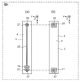
- Figure 4 is a plan view showing the wiring electrodes on the substrate 3.
- Figure 4(a) is a plan view showing the wiring electrodes on the first main surface 4 of the substrate 3.
- Figure 4(b) is a perspective plan view seen through the substrate 3, showing the wiring electrodes on the second main surface 5.
- the dashed and dotted lines in Figure 4 indicate through-hole connections.
- a first land 19 connected to a first terminal 8 of the RFIC chip 7 via solder 23, and a second land 21 connected to a second terminal 9 of the RFIC chip 7 via solder 23 are arranged on the first main surface 4 of the substrate 3.
- an electrode 27 that faces the first land 19 in the longitudinal direction of the substrate 3, and a conductor pattern 25 that connects the first land 19 and the electrode 27.
- the conductor pattern 25 is, for example, a straight line extending in the longitudinal direction of the substrate 3.
- a second interlayer connection conductor 57 and a first interlayer connection conductor 55 are formed to penetrate the inside of the substrate 3.
- the first interlayer connection conductor 55 is a conductive via that connects the electrode 27 and the first electrode 29.
- the second interlayer connection conductor 57 is a conductive via that connects the second land 21 and the second electrode 31.
- the first and second interlayer connection conductors 55, 57 are, for example, conductors formed by filling holes in the insulating substrate 3 with a conductive paste that has been solidified (metallized), but they may also be plated through holes.
- the first and second interlayer connection conductors 55, 57 are disposed opposite each other in the longitudinal direction of the third substrate.
- a first electrode 29 and a second electrode 31 are arranged on the second main surface 5 of the substrate 3, and are connected to the first end 44 and the second end 45 of the coil element 6, respectively.
- the first electrode 29 and the second electrode 31 face each other in the longitudinal direction of the substrate 3.
- the first terminal 8 of the RFIC chip 7 is connected to the first end 44 of the coil element 6 via the solder 23, the first land 19, the conductor pattern 25, the electrode 27, the first interlayer connection conductor 55, and the first electrode 29.
- the second terminal 9 of the RFIC chip 7 is connected to the second end 45 of the coil element 6 via the solder 23, the second land 21, the second interlayer connection conductor 57, and the second electrode 31.
- An LC parallel resonant circuit is configured within the RFID module 1 and is matched to radio waves of the communication frequency, so when the coil element 6 receives radio waves of the communication frequency, a current flows through the RFIC chip 7.
- the portion of the conductor 41 of the coil element 6 that contacts the second main surface 5 of the substrate 3 and the first electrode 29 and second electrode 31 on the second main surface are covered and protected by the resist layer 17. This makes it possible to prevent a short circuit between the metal outside the RFID module 1 and the coil element 6, the first electrode 29, and the second electrode 31, and to prevent an effect on the resonant frequency of the RFIC chip 7.
- the conductor 41 of the coil element 6 protrudes from inside one side of the resist layer 17 of the RFID module 1 to the outside, then winds around one side of the substrate 3 and the resin layer 10, the top surface of the resin layer 10, and the surface facing the one side of the substrate 3 and the resin layer 10, before again entering the inside from the surface facing the one side of the resist layer 17. In this way, the coil element 6 is wound around the outer circumference of the resin layer 10.
- the longitudinal section of the RFID module 1 perpendicular to the winding axis Wa of the coil element 6 is rectangular, so the opening P of the coil element 6 formed by the conductor 41 wound around a portion of the outer circumference of the RFID module 1 is also rectangular when viewed from the winding axis Wa, as shown in FIG. 5(a). Therefore, compared to the circular coil-shaped coil element 91 shown in FIG. 5(b), assuming that the diameter R of the circle and the length L of the side of the rectangle are the same, the opening area of the rectangular opening is larger, so the antenna characteristics of the RFID module 1 of embodiment 1 are better.
- the manufacturing procedure for the RFID module 1 will now be described.
- the first land 19, second land 21, conductor pattern 25, electrode 27, first electrode 29, and second electrode 31, which are conductors, are patterned on a large double-sided board, for example, by photolithography using copper foil.
- the wiring for multiple RFID modules 1 is patterned.
- an RFIC chip 7 is mounted on each of the first lands 19 and second lands 21, and the RFIC chip 7 on the substrate is molded with a resin layer 10.
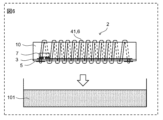
- the molded large double-sided substrate is singulated into modules one by one by dicing. At this time, barrel processing may be performed to remove the corners of the singulated modules.
- the second main surface 5 side of the substrate 3 of the singulated module 2 is immersed in, for example, a UV curable resin liquid 101, and the UV curable resin liquid 101 is attached to the second main surface 5 side and irradiated with UV light, thereby forming a resist layer 17 and manufacturing the RFID module 1.
- the RFID module 1 of the first embodiment includes the substrate 3, the first electrode 29 and the second electrode 31 arranged on the substrate 3, the coil element 6 connected at one end to the first electrode 29 and at the other end to the second electrode 31, the RFIC chip 7 electrically connected at one end to the first electrode 29 and at the other end to the second electrode 31, and the resin layer 10 covering the RFIC chip 7.
- the coil element 6 is wound around the substrate 3, and at least a portion of it is exposed to the outside of the resin layer 10.
- the coil spring By placing the RFID module 1 inside a metal coil spring, for example, the coil spring can be excited, thereby increasing the communication distance.
- the substrate 3 also has a first principal surface 4 and a second principal surface 5 facing each other, with the RFIC chip 7 disposed on the first principal surface 4 and the first electrode 29 and the second electrode 31 disposed on the second principal surface 5.
- the RFID module 1 has a resin layer 10 disposed on the first principal surface 4 that covers the RFIC chip 7, and a resist layer 17 disposed on the second principal surface 5 that covers the first electrode 29 and the second electrode 31.
- the coil element 6 is wound around the substrate 3 and the resin layer 10.
- Fig. 7 is a plan view showing an outline of an RFID module 1A according to a second embodiment.
- Fig. 8 is a cross-sectional view taken along line AA in Fig. 7.
- the substrate 3A in the second embodiment is a single-sided substrate.
- the configuration of the RFID module 1A in the second embodiment is the same as that of the RFID module 1 in the first embodiment, and a description of the common configuration will be omitted.
- the thickness of the substrate 3A in embodiment 2 is greater than the thickness of the substrate 3 in embodiment 1, for example, about 1 mm.
- the first land 19A extends from the center of the substrate 3A to one end in the longitudinal direction
- the second land 21A extends from the center of the substrate 3A to the other end in the longitudinal direction.
- the first end 44A of the coil element 6A is connected to one end of the first land 19A
- the second end 45A of the coil element 6A is connected to the other end of the second land 21A.
- the first land 19A on the center side of the substrate 3A is connected to the first terminal 8 of the RFIC chip 7 via solder 23.
- the second land 21A on the center side of the substrate 3A is connected to the second terminal 9 of the RFIC chip 7 via solder 23.
- an insulating resist layer 18 is laminated on the side opposite the substrate 3A, except for the connection portion with the first end 44A of the coil element 6A and the connection portion with the solder 23.
- an insulating resist layer 18 is laminated on the side opposite the substrate 3A, except for the connection portion with the second end 45A of the coil element 6A and the connection portion with the solder 23.
- the conductor 41 of the coil element 6A in embodiment 2 has a conductive core wire and an insulating film that covers the outer periphery of the core wire. In this case, it is also possible to communicate by placing the second main surface 5A of the RFID module 1A on a metal surface so that it faces the metal surface. In this case, the RFID module 1A can communicate by exciting the metal surface. If the conductor 41 is composed of only a core wire, a resin layer may be formed to cover the coil element 6A on the second main surface 5A side of the substrate 3A.
- an insulating resin layer 10A is laminated, covering the RFID module 1A, the first land 19A, the second land 21A, and the coil element 6A.
- the resin layer 10A does not need to be formed by resin molding, and may be formed, for example, from a UV-curable resin. In this case, the RFID module 1 can be manufactured inexpensively, as the resin layer is not formed by resin molding.
- the RFIC chip 7 is disposed at the center of the coil element 6A in the longitudinal direction in a plan view. Since the coil element 6A is disposed symmetrically around the RFIC chip 7, it is possible to obtain symmetric communication characteristics.
- the coil element 6A and the RFIC chip 7 do not overlap in a planar view. This reduces the effect of the magnetic field induced by the current flowing through the coil element 6A on the RFIC chip 7. It also reduces the load on the RFIC chip caused by the tension of the winding of the coil element.
- the substrate 3A has a first main surface 4A and a second main surface 5A that face each other, and the RFIC chip 7, a first land 19A as a first electrode, and a second land 21A as a second electrode are arranged on the first main surface 4A side.
- the coil element 6A is wound around the substrate 3A, and at least a portion of it is exposed to the outside of the resin layer 10A.
- the RFID module 1A of embodiment 2 like the RFID module 1 of embodiment 1, at least a portion of the coil element 6A is exposed to the outside of the resin layer 10A, improving the communication characteristics of the coil element 6 as an antenna.
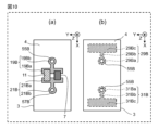
- Fig. 9 is a plan view showing an outline of an RFID module 1B according to the third embodiment, from which a coil element is omitted.
- Fig. 10 is a plan view showing electrodes arranged on a substrate 3.
- connection point between the interlayer connection conductor and the electrode disposed on the second main surface 5 of the substrate 3 is offset from the connection point between this electrode and the coil element 6.
- the configuration of the RFID module 1B of the third embodiment is the same as that of the RFID module 1 of the first embodiment, and a description of the common configuration will be omitted.
- a first land 19B connected to the first terminal 8 of the RFIC chip 7 via solder 23, and a second land 21B connected to the second terminal 9 of the RFIC chip 7 via solder 23 are arranged on the first main surface 4, which is the upper surface of the substrate 3.
- the first land 19B has an electrode 19Ba connected to the first terminal 8 of the RFIC chip 7, and an electrode 19Bb extending outward from the electrode 19Ba in the longitudinal direction of the substrate 3.
- the tip of the electrode 19Bb is connected to the upper end of the first interlayer connection conductor 55B that penetrates the substrate 3, and the lower end of the first interlayer connection conductor 55B is connected to the first electrode 29B arranged on the second main surface 5, which is the lower surface of the substrate 3.
- the second land 21B has an electrode 21Ba connected to the second terminal 9 of the RFIC chip 7, and an electrode 21Bb extending outward from the electrode 21Ba in the longitudinal direction of the substrate 3.
- the tip of the electrode 21Bb is connected to the upper end of the second interlayer connection conductor 57B that penetrates the substrate 3, and the lower end of the second interlayer connection conductor 57B is connected to the second electrode 31B arranged on the second main surface 5, which is the lower surface of the substrate 3.
- the first electrode 29B arranged on the second main surface 5 of the substrate 3 has an electrode 29Ba connected to the first interlayer connection conductor 55B, a wiring 29Bb extending from the electrode 29Ba toward the outside in the longitudinal direction of the substrate 3, and an electrode 29Bc connected to the outer end of the wiring 29Bb.
- the electrode 29Bc is connected to the first end 44 of the coil element 6.
- the second electrode 31B arranged on the second main surface 5 of the substrate 3 has an electrode 31Ba connected to the second interlayer connection conductor 57B, a wiring 31Bb extending from the electrode 31Ba toward the outside in the longitudinal direction of the substrate 3, and an electrode 31Bc connected to the outer end of the wiring 31Bb.
- the electrode 31Bc is connected to the second end 45 of the coil element 6.
- the electrode 29Ba and wiring 29Bb of the first electrode 29B are covered and protected by a resist layer 61.
- the electrode 31Ba and wiring 31Bb of the second electrode 31B are covered and protected by a resist layer 61.
- the connection portions between the coil element 6 and the respective electrodes 29Bc, 31Bc arranged on the second main surface 5 of the substrate 3 are exposed and are not covered by the resist layer 61.
- the first terminal 8 of the RFIC chip 7 is connected to the first end 44 of the coil element 6 via the solder 23, the first land 19B, the first interlayer connection conductor 55B, and the first electrode 29B.
- the second terminal 9 of the RFIC chip 7 is connected to the second end 45 of the coil element 6 via the solder 23, the second land 21B, the second interlayer connection conductor 57B, and the second electrode 31B.
- the step in the interlayer connection conductor may affect the connection with the coil element.
- the RFID module 1B of embodiment 3 includes a first interlayer connection conductor 55B that connects the RFIC chip 7 and the first electrode 29B by penetrating the substrate 3, and a second interlayer connection conductor 57B that connects the RFIC chip 7 and the second electrode 31B by penetrating the substrate 3.
- Electrode 29Bc which is the connection point between the first electrode 29B and the coil element 6, is located further outward in the longitudinal direction of the substrate 3 than electrode 29Ba, which is the connection point between the first electrode 29B and the first interlayer connection conductor 55B.
- Electrode 31Bc which is the connection point between the second electrode 31B and the coil element 6, is located further outward in the longitudinal direction of the substrate 3 than electrode 31Ba, which is the connection point between the second electrode 31B and the second interlayer connection conductor 57B.
- the electrode 29Ba connected to the first interlayer connection conductor 55B and the electrode 29Bc connected to the first end 44 of the coil element 6 are located apart from each other, so that the step at the connection portion between the first interlayer connection conductor 55B and the electrode 29Ba can be prevented from affecting the connection between the first end 44 of the coil element 6 and the electrode 29Bc.
- the step at the connection portion between the second interlayer connection conductor 57B and the electrode 31Ba can be prevented from affecting the connection between the second end 45 of the coil element 6 and the electrode 31Bc.
- a matching capacitor 11 is connected in parallel to the RFIC chip 7 to the electrode 19Ba of the first land 19B and the electrode 21Ba of the second land 21B.
- the resonant frequency of the RFID module 1B can be reduced by the capacitance component of the capacitor 11. Note that the RFID module 1B may be configured without the capacitor 11.
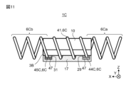
- Fig. 11 is a side view showing an outline of an RFID module 1C according to a third embodiment.
- Fig. 12 is a vertical cross-sectional view of the RFID module 1C.
- Fig. 13 is an equivalent circuit diagram of the RFID module 1C.
- the coil element 6C in the fourth embodiment extends in the longitudinal direction of the substrate 3 while winding outward beyond the substrate 3 and the resin layer 10.
- the configuration of the RFID module 1C in the fourth embodiment is the same as that of the RFID module 1 in the first embodiment or the RFID module 1B in the third embodiment, and a description of the common configuration will be omitted.
- a first land 19C connected to the first terminal 8 of the RFIC chip 7 via solder 23, and a second land 21C connected to the second terminal 9 of the RFIC chip 7 via solder 23 are arranged on the first main surface 4, which is the upper surface of the substrate 3.
- the outer end of the first land 19C in the longitudinal direction of the substrate 3 is connected to the upper end of the first interlayer connection conductor 55 that penetrates the substrate 3, and the lower end of the first interlayer connection conductor 55 is connected to the first electrode 29 arranged on the second main surface 5 of the substrate 3.
- the first electrode 29 is joined to the first connection portion 44C of the coil element 6C, for example, by solder 47.
- the first electrode 29 and the first connection portion 44C of the coil element 6C may be joined electrically by welding or ultrasonic waves, other than by solder 47.
- the outer end of the second land 21C in the longitudinal direction of the substrate 3 is connected to the upper end of the second interlayer connection conductor 57 that penetrates the substrate 3, and the lower end of the second interlayer connection conductor 57 is connected to the second electrode 31 arranged on the second main surface 5 of the substrate 3.
- the second electrode 31 is joined to the second connection portion 45C of the coil element 6C, for example, by solder 47.
- the second electrode 31 and the second connection portion 45C of the coil element 6C may be joined electrically by welding or ultrasonic waves, other than by solder 47.
- the RFIC chip 7 has a power supply point 7a and a capacitance C1 inside.
- a first terminal 8 electrically connected to one of the power supply point 7a and the capacitance C1 is connected to the first connection portion 44C of the coil element 6C via the solder 23, the first land 19C, the first interlayer connection conductor 55, and the first electrode 29.
- a second terminal 9 electrically connected to the other of the power supply point 7a and the capacitance C1 is connected to the second connection portion 45C of the coil element 6C via the solder 23, the second land 21C, the second interlayer connection conductor 57, and the second electrode 31.
- the coil element 6C has a first coil extension 6Ca and a second coil extension 6Cb that protrude further in the longitudinal direction of the substrate 3 than the substrate 3 and the resin layer 10, respectively. This allows the coil element 6C to function as a dipole antenna, thereby further improving communication performance.
- the coil element 6C has a first coil extension 6Ca on one side that extends from the connection with the first electrode 29 further outward from the substrate 3, and a second coil extension 6Cb on the other side that extends from the connection with the second electrode 31 further outward from the substrate 3 in the opposite direction to the extension of the first coil extension 6Ca. This can further improve the communication performance of the RFID module 1C.
- the RFIC chip 7 is arranged at the end of the substrate 3, but this is not limited to this.
- the RFIC chip 7 may be arranged in the center of the substrate 3 together with the first land 19 and the second land 21. This places the RFIC chip 7 in the longitudinal center of the coil element 6 in a planar view.
- the coil element 6 is arranged symmetrically around the RFIC chip 7, symmetrical communication characteristics can be obtained.
- the load transmitted to the RFIC chip 7 when connecting the coil element 6 to the first electrode 29 and the second electrode 31 can be reduced.
- the RFID module of the first aspect of the present invention comprises a substrate, a first electrode and a second electrode arranged on the substrate, a coil element having one end connected to the first electrode and the other end connected to the second electrode, an RFIC chip having one end electrically connected to the first electrode and the other end electrically connected to the second electrode, and a first insulating layer covering the RFIC chip.
- the coil element is wound around the substrate, and at least a portion of it is exposed to the outside of the first insulating layer.
- the coil element is exposed to the outside of the first insulating layer, so that a portion of the coil element reaches the outer periphery of the RFID module, allowing the opening of the coil element to be made wider. This allows a magnetic field to be radiated widely from the coil element, improving the communication characteristics of the coil element as an antenna.
- the coil element has a conductor wound multiple times, and the winding pitch of the conductor is larger than the wire diameter of the conductor.
- the coil element has gaps between adjacent wound conductors, so that the magnetic field generated by the coil element is easily released to the outside and magnetic field coupling is easily achieved, thereby improving communication characteristics.
- the substrate has a first main surface and a second main surface facing each other, an RFIC chip is disposed on the first main surface side, a first electrode and a second electrode are disposed on the second main surface side, a first insulating layer covering the RFIC chip is disposed on the first main surface, and a second insulating layer is provided on the second main surface covering at least a portion of the first electrode and the second electrode, and the coil element is wound around the substrate and the first insulating layer.
- the cross section of the first insulating layer perpendicular to the winding axis of the coil element is rectangular. Since the opening of the coil element can be made rectangular, the communication characteristics can be improved compared to a coil element with a circular opening.
- the substrate of the first or second aspect has a first main surface and a second main surface that face each other, and the RFIC chip, the first electrode, and the second electrode are arranged on the first main surface side.
- the RFIC chip is disposed in the longitudinal center of the coil element in a plan view. This allows the coil elements to be disposed symmetrically around the RFIC chip, thereby making it possible to obtain symmetrical communication characteristics.
- the coil element and the RFIC chip do not overlap in a plan view on the first main surface side of the substrate. This makes it possible to reduce the influence of the magnetic field induced by the current flowing through the coil element on the RFIC chip.
- the RFID module of the third aspect includes a first interlayer connection conductor that connects the RFIC chip and the first electrode through the substrate, and a second interlayer connection conductor that connects the RFIC chip and the second electrode through the substrate.
- the connection point between the first electrode and the coil element is located outside the connection point between the first electrode and the first interlayer connection conductor in the longitudinal direction of the substrate, and the connection point between the second electrode and the coil element is located outside the connection point between the second electrode and the second interlayer connection conductor in the longitudinal direction of the substrate.
- the coil element has a first coil extension on one side that extends from the connection with the first electrode further outward from the substrate 3, and a second coil extension on the other side that extends from the connection with the second electrode further outward from the substrate 3 in the opposite direction to the extension of the first coil extension. This can improve communication characteristics.
Landscapes
- Engineering & Computer Science (AREA)
- Computer Hardware Design (AREA)
- Microelectronics & Electronic Packaging (AREA)
- Physics & Mathematics (AREA)
- General Physics & Mathematics (AREA)
- Theoretical Computer Science (AREA)
- Coils Or Transformers For Communication (AREA)
Priority Applications (2)
| Application Number | Priority Date | Filing Date | Title |
|---|---|---|---|
| CN202380064579.5A CN119856340A (zh) | 2022-11-14 | 2023-11-13 | Rfid模块 |
| JP2024558849A JP7733359B2 (ja) | 2022-11-14 | 2023-11-13 | Rfidモジュール |
Applications Claiming Priority (2)
| Application Number | Priority Date | Filing Date | Title |
|---|---|---|---|
| JP2022181845 | 2022-11-14 | ||
| JP2022-181845 | 2022-11-14 |
Publications (1)
| Publication Number | Publication Date |
|---|---|
| WO2024106370A1 true WO2024106370A1 (ja) | 2024-05-23 |
Family
ID=91084355
Family Applications (1)
| Application Number | Title | Priority Date | Filing Date |
|---|---|---|---|
| PCT/JP2023/040716 Ceased WO2024106370A1 (ja) | 2022-11-14 | 2023-11-13 | Rfidモジュール |
Country Status (3)
| Country | Link |
|---|---|
| JP (1) | JP7733359B2 (https=) |
| CN (1) | CN119856340A (https=) |
| WO (1) | WO2024106370A1 (https=) |
Citations (2)
| Publication number | Priority date | Publication date | Assignee | Title |
|---|---|---|---|---|
| JP2011004427A (ja) * | 2003-04-15 | 2011-01-06 | Sensors For Medicine & Science Inc | 一体化されたアンテナを備えたプリント回路装置及びプリント集積回路基板アンテナを備えた埋め込み可能なセンサー処理装置 |
| WO2017141663A1 (ja) * | 2016-02-17 | 2017-08-24 | 株式会社村田製作所 | 無線通信デバイス、及びその製造方法 |
Family Cites Families (4)
| Publication number | Priority date | Publication date | Assignee | Title |
|---|---|---|---|---|
| JP2005149189A (ja) | 2003-11-17 | 2005-06-09 | Matsushita Electric Ind Co Ltd | データキャリアおよびその製造方法 |
| CN207124291U (zh) | 2015-02-03 | 2018-03-20 | 株式会社村田制作所 | 天线装置以及电子设备 |
| JP6648830B2 (ja) | 2016-07-01 | 2020-02-14 | 株式会社村田製作所 | コイルモジュール |
| DE112017006123T5 (de) | 2016-12-02 | 2019-09-26 | Murata Manufacturing Co., Ltd. | RFID-Etikett |
-
2023
- 2023-11-13 WO PCT/JP2023/040716 patent/WO2024106370A1/ja not_active Ceased
- 2023-11-13 JP JP2024558849A patent/JP7733359B2/ja active Active
- 2023-11-13 CN CN202380064579.5A patent/CN119856340A/zh active Pending
Patent Citations (2)
| Publication number | Priority date | Publication date | Assignee | Title |
|---|---|---|---|---|
| JP2011004427A (ja) * | 2003-04-15 | 2011-01-06 | Sensors For Medicine & Science Inc | 一体化されたアンテナを備えたプリント回路装置及びプリント集積回路基板アンテナを備えた埋め込み可能なセンサー処理装置 |
| WO2017141663A1 (ja) * | 2016-02-17 | 2017-08-24 | 株式会社村田製作所 | 無線通信デバイス、及びその製造方法 |
Also Published As
| Publication number | Publication date |
|---|---|
| JPWO2024106370A1 (https=) | 2024-05-23 |
| CN119856340A (zh) | 2025-04-18 |
| JP7733359B2 (ja) | 2025-09-03 |
Similar Documents
| Publication | Publication Date | Title |
|---|---|---|
| JP6119845B2 (ja) | 高周波部品およびこれを備える高周波モジュール | |
| CN101657938B (zh) | 磁场耦合型天线、磁场耦合型天线模块及磁场耦合型天线装置、及这些的制造方法 | |
| US8602310B2 (en) | Radio communication device and radio communication terminal | |
| US10374305B2 (en) | Multilayer substrate and electronic device | |
| US10672554B2 (en) | Inductor component and method for manufacturing the same | |
| JP6380648B2 (ja) | コイルデバイスおよび電子デバイス | |
| CN109300643B (zh) | 线圈部件及其制造方法 | |
| US7081804B2 (en) | Chip coil | |
| JP6648830B2 (ja) | コイルモジュール | |
| JP7733359B2 (ja) | Rfidモジュール | |
| WO2017159436A1 (ja) | コイルモジュール | |
| WO2025100050A1 (ja) | Rfidモジュール | |
| JPWO2014069107A1 (ja) | 部品内蔵基板および通信端末装置 | |
| WO2017131011A1 (ja) | インダクタ部品およびその製造方法 | |
| US10506717B2 (en) | Inductor component and method of manufacturing inductor component | |
| JP6015813B2 (ja) | 多層回路モジュール | |
| US20250117621A1 (en) | Rfid module | |
| US12232269B2 (en) | Electronic component module | |
| CN116864494B (zh) | 扇出型封装结构和扇出型封装结构制作方法 | |
| CN217405707U (zh) | 无线通信模块 | |
| JP6662497B1 (ja) | Rfidタグ及びその製造方法 | |
| WO2011118072A1 (ja) | 回路基板 | |
| JP2009049325A (ja) | 電子部品モジュール及びその製造方法 | |
| WO2026053597A1 (ja) | Rfidモジュール及び無線通信デバイス | |
| HK1206146B (en) | Circuit module |
Legal Events
| Date | Code | Title | Description |
|---|---|---|---|
| 121 | Ep: the epo has been informed by wipo that ep was designated in this application |
Ref document number: 23891517 Country of ref document: EP Kind code of ref document: A1 |
|
| WWE | Wipo information: entry into national phase |
Ref document number: 2024558849 Country of ref document: JP |
|
| WWE | Wipo information: entry into national phase |
Ref document number: 202380064579.5 Country of ref document: CN |
|
| WWP | Wipo information: published in national office |
Ref document number: 202380064579.5 Country of ref document: CN |
|
| NENP | Non-entry into the national phase |
Ref country code: DE |
|
| 122 | Ep: pct application non-entry in european phase |
Ref document number: 23891517 Country of ref document: EP Kind code of ref document: A1 |