WO2024100726A1 - 高周波回路および半導体装置 - Google Patents
高周波回路および半導体装置 Download PDFInfo
- Publication number
- WO2024100726A1 WO2024100726A1 PCT/JP2022/041422 JP2022041422W WO2024100726A1 WO 2024100726 A1 WO2024100726 A1 WO 2024100726A1 JP 2022041422 W JP2022041422 W JP 2022041422W WO 2024100726 A1 WO2024100726 A1 WO 2024100726A1
- Authority
- WO
- WIPO (PCT)
- Prior art keywords
- substrate
- frequency circuit
- circuit according
- convex portion
- protrusion
- Prior art date
- Legal status (The legal status is an assumption and is not a legal conclusion. Google has not performed a legal analysis and makes no representation as to the accuracy of the status listed.)
- Ceased
Links
Images







Classifications
-
- H—ELECTRICITY
- H01—ELECTRIC ELEMENTS
- H01P—WAVEGUIDES; RESONATORS, LINES, OR OTHER DEVICES OF THE WAVEGUIDE TYPE
- H01P1/00—Auxiliary devices
-
- H—ELECTRICITY
- H01—ELECTRIC ELEMENTS
- H01P—WAVEGUIDES; RESONATORS, LINES, OR OTHER DEVICES OF THE WAVEGUIDE TYPE
- H01P1/00—Auxiliary devices
- H01P1/04—Fixed joints
-
- H—ELECTRICITY
- H10—SEMICONDUCTOR DEVICES; ELECTRIC SOLID-STATE DEVICES NOT OTHERWISE PROVIDED FOR
- H10W—GENERIC PACKAGES, INTERCONNECTIONS, CONNECTORS OR OTHER CONSTRUCTIONAL DETAILS OF DEVICES COVERED BY CLASS H10
- H10W70/00—Package substrates; Interposers; Redistribution layers [RDL]
- H10W70/60—Insulating or insulated package substrates; Interposers; Redistribution layers
-
- H—ELECTRICITY
- H10—SEMICONDUCTOR DEVICES; ELECTRIC SOLID-STATE DEVICES NOT OTHERWISE PROVIDED FOR
- H10W—GENERIC PACKAGES, INTERCONNECTIONS, CONNECTORS OR OTHER CONSTRUCTIONAL DETAILS OF DEVICES COVERED BY CLASS H10
- H10W72/00—Interconnections or connectors in packages
Definitions
- This disclosure relates to high-frequency circuits and semiconductor devices.
- Patent Document 1 discloses a filter in which a microstrip line is formed.
- This filter comprises a dielectric substrate, a microstrip conductive metal film formed on the front surface of the dielectric substrate, and a back surface metal film formed over the entire back surface of the dielectric substrate. Directly below the microstrip conductive metal film inside the dielectric substrate, multiple internal spaces are formed at predetermined intervals along the extension direction of the microstrip conductive metal film.
- One method of miniaturizing microwave and millimeter wave circuits is to make the substrate thinner.
- the substrate is thinned from 100 ⁇ m to 50 ⁇ m, for example, the width of the microstrip lines on the top surface of the chip can be reduced for the same characteristic impedance. This allows the area occupied by the matching circuit to be reduced.
- the conductive resin may creep up onto the top surface of the chip. This may make it difficult to mount with a high yield. Furthermore, conductive resin that creeps up onto the top surface of the chip may unintentionally short out the pattern, preventing the chip from functioning. Furthermore, conductive resin adhering to the pads may cause problems such as insufficient wire bond strength being obtained.
- the objective of this disclosure is to obtain a high-frequency circuit and semiconductor device that can prevent bonding material from creeping up onto the top surface of the substrate.
- the high-frequency circuit according to the present disclosure comprises a substrate and a signal line provided on an upper surface of the substrate, and a first protrusion is formed on the outer periphery of the back surface of the substrate opposite the upper surface along at least two opposing sides of the substrate.
- the first convex portion when the high-frequency circuit is mounted using a bonding material, can increase the distance from the application surface of the bonding material to the top surface of the substrate. This can therefore prevent the bonding material from creeping up onto the top surface of the substrate.
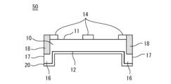
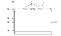
- FIG. 1 is a cross-sectional view of a high-frequency circuit according to a first embodiment. 4 is a diagram illustrating the configuration of the back side of the high-frequency circuit according to the first embodiment.
- FIG. 1 is a cross-sectional view of a high-frequency circuit according to a first comparative example.
- FIG. 11 is a cross-sectional view of a high-frequency circuit according to a second comparative example.
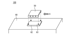
- 1 is a perspective view illustrating a configuration of a semiconductor device according to a first embodiment
- 1 is a side view of a semiconductor device according to a first embodiment
- FIG. 2 is a perspective view illustrating a configuration of a wafer according to the first embodiment.
- FIG. 11 is a cross-sectional view of a high-frequency circuit according to a second embodiment. 11 is a diagram illustrating the configuration of the back side of a high-frequency circuit according to a second embodiment.
- FIG. 11 is a perspective view illustrating a configuration of a semiconductor device according to a second embodiment.
- FIG. 11 is a side view of a semiconductor device according to a second embodiment.
- FIG. 11 is a cross-sectional view of a high-frequency circuit according to a third embodiment.
- 13 is a diagram illustrating the configuration of the back side of the high-frequency circuit according to the third embodiment.
- FIG. 13 is an enlarged view of a high-frequency circuit according to a fourth embodiment.
- FIG. 13 is an enlarged view of a high-frequency circuit according to a fifth embodiment.
- 13 is a diagram illustrating the configuration of the back side of a high-frequency circuit according to a sixth embodiment.
- FIG. 13 is a diagram illustrating the configuration of the back side of a high-frequency circuit according to a modified example of the sixth embodiment.
- FIG. FIG. 13 is a cross-sectional view of a high-frequency circuit according to a seventh embodiment. 13 is a diagram illustrating the configuration of the back side of the high-frequency circuit according to the seventh embodiment.
- Fig. 1 is a cross-sectional view of a high-frequency circuit 50 according to a first embodiment.
- Fig. 2 is a diagram for explaining the configuration of the back side of the high-frequency circuit 50 according to the first embodiment.
- the high-frequency circuit 50 is, for example, a micro/millimeter wave band MMIC (Monolithic Microwave Integrated Circuit) chip.
- the high-frequency circuit 50 includes a substrate 10 and a signal line 14 provided on an upper surface 11 of the substrate 10.
- the substrate 10 is, for example, a SiC substrate.
- the signal line constitutes, for example, a microstrip line.
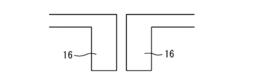
- protrusions 16 are formed along each of the two opposing sides of the substrate 10.
- the substrate 10 is thinned, leaving only the portions along the two opposing sides that are the periphery of the circuit.
- no protrusions are formed along the other two sides of the outer periphery of the back surface 12 of the substrate 10 other than the two sides on which the protrusions 16 are formed.
- the length of one side of the high-frequency circuit 50 is, for example, 5 mm or less.
- the thickness of the thick portion of the substrate 10 is, for example, 100 ⁇ m to 200 ⁇ m.
- the thickness of the thinned portion of the substrate 10 is, for example, 50 ⁇ m or less, specifically 10 ⁇ m to 50 ⁇ m.
- the width of the protrusion 16 is, for example, about 50 to 200 ⁇ m.
- Pads 18 are provided on the side surfaces 17 of the substrate 10 corresponding to the two sides on which the protrusions 16 are formed.
- the pads 18 are DC or RF pads.
- the rear surface 12 of the substrate 10 is covered with a conductor layer 20 that serves as GND.
- FIG. 3 is a cross-sectional view of a high-frequency circuit 50a according to a first comparative example.
- FIG. 4 is a cross-sectional view of a high-frequency circuit 50b according to a second comparative example.
- the substrate 10a of the high-frequency circuit 50a has a thickness of 100 ⁇ m.
- a signal line 14 is provided on the upper surface of the substrate 10a.
- a conductor layer 20 serving as GND is provided on the rear surface of the substrate 10a.
- the substrate 10b of the high-frequency circuit 50b has a thickness of 50 ⁇ m.
- a signal line 14 is provided on the upper surface of the substrate 10b.
- a conductor layer 20 serving as GND is provided on the rear surface of the substrate 10b.
- the width of the signal line 14 will be smaller in the high-frequency circuit 50b, which has a thinner substrate 10b, and W1>W2.
- low-impedance lines are generally used for the output combining circuit in the final stage of a power amplifier. If the line width of the matching circuit can be reduced while maintaining the same characteristic impedance, the area of the output combining circuit can be reduced. This makes it possible to achieve a smaller overall MMIC.
- the convex portion 16 can increase the distance from the application surface of the bonding material, such as conductive resin, to the top surface 11 of the substrate 10.
- the substrate 10 is gripped by the two thick sides, ensuring the distance from the tip of the tweezers, collet, etc. to the application surface of the conductive resin. This can prevent the bonding material from creeping up onto the top surface 11 of the substrate 10 via the tweezers, collet, etc.
- the substrate 10 can be made thinner to reduce the size of the high-frequency circuit 50, and the high-frequency circuit 50 can be mounted with a high yield.
- the spread of the conductive resin can be confirmed from the two sides of the substrate 10 where the protrusions 16 are not formed. Therefore, it is possible to visually confirm that the die bonding has been performed reliably. Furthermore, by providing the pads 18 for DC or RF extraction on the side surface 17 of the substrate 10 instead of the top surface 11, the MMIC chip can be further miniaturized.
- the signal line will branch into multiple lines, such as a T-branch structure or a cross-branch structure, at the area where the characteristic impedance changes, specifically at the boundary between the locally thinned area and the thick part of the substrate. In such a case, parasitic components are added, and it may be difficult to achieve the performance in a terahertz wave band circuit.
- the central portion of the substrate 10 where the circuit is formed is uniformly thinned, as in this embodiment.
- a part of the signal line 14 is disposed directly above the convex portion 16.
- the signal line 14 directly above the convex portion 16 is a line or pad for applying a DC bias
- the effect of the change in the characteristic impedance of the signal line 14 on the circuit characteristics is generally small. This is because the RF signal component of interest is appropriately processed in the circuit or in a peripheral circuit outside the MMIC.
- the change in the characteristic impedance that is, the change in the distance between the signal line 14 and the GND conductor, may affect the characteristics. For this reason, it may be necessary to grasp the effect in advance by electromagnetic field simulation or the like and to carry out an appropriate design such as changing the signal line width.
- the convex portion 16 may be provided to avoid the portion where the circuit is formed, particularly the main line through which an RF signal passes or the RF probe pad.
- the signal line 14 directly above the protrusion 16 may be a line or pad for applying a DC bias.
- the heat dissipation of the transistors can be improved.
- the VH (via hole) diameter can be reduced, making it easier to further miniaturize the circuit.
- VHs are usually excavated by dry etching. For this reason, if the amount of excavation, i.e. the substrate thickness, is small, the VH diameter can be made smaller.
- FIG. 5 is a perspective view for explaining the configuration of the semiconductor device 100 according to the first embodiment.
- FIG. 6 is a side view of the semiconductor device 100 according to the first embodiment.
- FIG. 6 is a view of FIG. 5 as viewed from the A direction.
- the semiconductor device 100 includes a high-frequency circuit 50, a mounting substrate 60, and a protrusion 62 provided on the mounting substrate 60.
- the protrusion 62 is fitted between the convex portions 16 of the high-frequency circuit 50.
- the protrusion 62 has a shape corresponding to the recess in the rear surface 12 of the substrate 10.
- the upper surface 63 of the protrusion 62 is the bonding surface with the rear surface 12 of the high-frequency circuit 50, that is, the portion coated with the conductive resin.
- the mounting substrate 60 is also called a die-bond substrate.
- the semiconductor device 100 can ensure a large distance between the top surface 63 of the protrusion 62 and the top surface 11 of the substrate 10 of the high frequency circuit 50. This can prevent the conductive resin from being sucked up by tweezers or the like, allowing for high mounting yields.
- the height of the protrusion 62 is preferably about 50 ⁇ m longer than the recess dimension on the back surface 12 of the high frequency circuit 50. This allows most of the conductive resin that protrudes outside the chip to creep up on the mounting substrate 60 around the protrusion 62, rather than toward the tip of the tweezers or the like. This can sufficiently reduce the risk of the conductive resin creeping up onto the top surface of the chip.
- FIG. 7 is a perspective view explaining the configuration of a wafer 80 according to the first embodiment.
- FIG. 7 shows the state before the substrate 10 of this embodiment is separated into chips.
- the wafer 80 has protrusions 81 and 82, which are thick portions of the wafer 80.
- the protrusion 81 corresponds to the protrusion 16 of the high-frequency circuit 50.
- the width of the protrusion 81 is, for example, 100 to 400 ⁇ m.
- the protrusion 82 is a dummy portion provided for the purpose of reinforcing the strength and warping of the wafer 80.
- the width of the protrusion 82 is, for example, 100 to 400 ⁇ m.
- the wafer may warp, making it impossible to fix the wafer to the stage when inspecting its characteristics in the wafer state. In addition, it may become difficult to attach the wafer to tape and perform wafer dicing. Furthermore, if the wafer is fixed to a flat stage or the like in a warped state, the wafer may break or crack, resulting in a decrease in yield.
- the substrate thickness may be set to 30 ⁇ m or less. Achieving this substrate thickness with a wafer of 4 inches or more in diameter is even more difficult because, in addition to the problems of conductive resin creeping up and wafer warping, the wafer may crack when handled due to reduced strength.
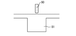
- FIG. 8 is a diagram illustrating the state of the convex portion 81 of the wafer 80 according to the first embodiment before dicing.
- FIG. 9 is a diagram illustrating the state of the convex portion 81 of the wafer according to the first embodiment after dicing. In dicing, a dimension equivalent to the width of the dicing blade 90 used to cut the wafer 80 is removed. The width of the convex portion 81 in the wafer state is approximately the sum of the width of two convex portions 16 after dicing and the width of the dicing blade 90.
- the substrate 10 may be formed from a material other than SiC.
- the high frequency circuit 50 is not limited to an MMIC, but may be a matching circuit, a filter, etc.
- the bonding material for bonding the high frequency circuit 50 and the protrusion 62 is not limited to conductive resin, but may be solder, etc.
- the convex portions 16 are not limited to being formed on the two opposing sides of the substrate 10, but may also be formed on other sides. In other words, it is sufficient that the convex portions 16 are formed at least along each of the two opposing sides of the substrate 10.
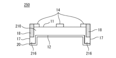
- Fig. 10 is a cross-sectional view of a high-frequency circuit 250 according to the second embodiment.
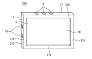
- Fig. 11 is a diagram for explaining the configuration of the back surface side of a high-frequency circuit 250 according to the second embodiment.
- the location where the convex portion 216 is formed is different from that of the first embodiment.
- the other configurations are similar to those of the first embodiment.
- the convex portion 216 is formed along the four sides of the substrate 210 on the outer periphery of the back surface 12 of the substrate 210.
- the annular convex portion 216 is formed on the outer periphery of the substrate 210.
- the protrusions 216 can increase the distance from the surface on which the conductive resin is applied to the top surface of the substrate. This can prevent the bonding material from creeping up onto the top surface of the substrate 210. This allows the substrate 210 to be made thinner, the high frequency circuit 50 to be made smaller, and the high frequency circuit 250 to be mounted with a high yield. Note that in this embodiment, the outer periphery of the substrate 210 is made thick on all four sides, so the spread of the conductive resin can be confirmed by the conductive resin spilling out of the substrate 210. The conductive resin spilling out appears on the mounting substrate 60.
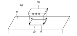
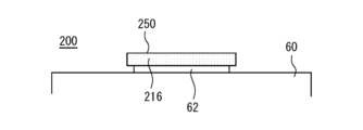
- FIG. 12 is a perspective view for explaining the configuration of a semiconductor device 200 according to the second embodiment.
- FIG. 13 is a side view of the semiconductor device 200 according to the second embodiment.
- the convex portion 216 provided along the four sides of the substrate 210 surrounds the protrusion 62 on the mounting substrate 60. This allows the high-frequency circuit 250 to be positioned, improving the positional accuracy of mounting.
- the direction in which the chip is gripped can be selected from two directions. Therefore, the effect of this embodiment can be obtained even when the direction in which the chip is gripped is restricted, such as when the mounting space is narrow.
- convex portions 216 are formed along the four sides of the substrate 210. Therefore, both convex portions 81 and 82 in the wafer 80 shown in FIG. 7 form convex portions 216.
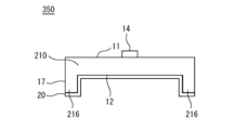
- Fig. 14 is a cross-sectional view of a high-frequency circuit 350 according to the third embodiment.
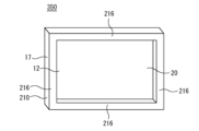
- Fig. 15 is a diagram for explaining the configuration of the back side of the high-frequency circuit 350 according to the third embodiment.
- This embodiment differs from the second embodiment in that the pads 18 are not provided on the side surfaces of the substrate 210.
- the other configurations are the same as those of the second embodiment. In such a case, the pads 18 are disposed on the upper surface 11 of the substrate 210. Even if the pads 18 are not provided on the side surfaces 17, the effect of suppressing the creeping up of the resin is maintained.
- pads 18 are not provided on the side surface 17 of the substrate 210 in embodiment 2, but pads 18 do not have to be provided on the side surface 17 of the substrate 10 in embodiment 1.
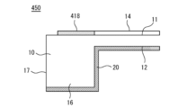
- Embodiment 4. 16 is an enlarged view of a radio frequency circuit 450 according to the fourth embodiment.
- an RF pad 418 is provided directly on the protrusion 16, not on the side surface 17 of the substrate 10.
- the other configurations are the same as those of the first embodiment. This makes it possible to reduce the capacitance between the RF pad 418 and the conductor layer 20, thereby improving the accuracy of on-wafer measurement.
- the RF pad 418 becomes the electrode pad of the transistor.
- the performance of the transistor can be improved by reducing the pad capacitance.
- pads may be provided both on the side surface 17 of the substrate 10 and directly above the protrusion 16.
- Fig. 17 is an enlarged view of a high-frequency circuit 550 according to the fifth embodiment.
- the convex portion 16 is formed inside the outermost periphery of the rear surface 12 of the substrate 510.
- the substrate 510 has a thinned inner recess 522 outside the convex portion 16.
- the inner recess 522 is a portion indicated by a length L1 in Fig. 17.
- the other configurations are the same as those of the fourth embodiment.
- the substrate 510 can be made thinner at the cut portion by dicing. Therefore, dicing can be easily performed.
- the distance from the tip of the tweezers, collet, etc. to the surface to which the conductive resin is applied can be further increased. Therefore, creeping up of the conductive resin can be further suppressed.
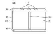
- Embodiment 6. 18 is a diagram illustrating the configuration of the back side of a high-frequency circuit 650 according to embodiment 6.
- a convex portion 624 is further formed in the center of the back surface 12 of the substrate 610.
- the other configurations are similar to those of embodiment 1.
- the convex portion 624 extends from one convex portion 16 to the other convex portion 16, for example, in the center of the substrate 610 in the longitudinal direction.
- the effect of suppressing warping of the wafer can be improved. According to this embodiment, it is possible to suppress a decrease in the strength of the chip, particularly when the thinned region is large. Furthermore, when the aspect ratio of the length and width of the chip is large, it is possible to suppress a decrease in the strength of the chip by forming a protrusion 624 midway along the long side of the chip.
- FIG. 19 is a diagram illustrating the configuration of the back side of a high-frequency circuit 750 according to a modified example of embodiment 6.
- a convex portion 624 is formed in the center of the back side 12 of the substrate 710.
- the convex portion 624 of this embodiment is not limited to the convex portion 16 of embodiment 1, and may be combined with the convex portion 216 of embodiment 2.
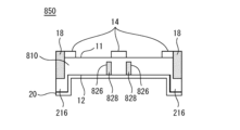
- Fig. 20 is a cross-sectional view of a high-frequency circuit 850 according to the seventh embodiment.
- Fig. 21 is a diagram for explaining the configuration of the back side of the high-frequency circuit 850 according to the seventh embodiment.
- a hole 826 is formed on the back surface 12 of the substrate 810 directly below the edge of the signal line 14.
- the hole 826 is filled with a metal 828.
- the other configuration is the same as that of the second embodiment.
- the hole 826 has a diameter of, for example, 15 ⁇ m.
- the multiple holes 826 are formed at intervals of approximately 35 ⁇ m.
- the substrates according to the first to sixth embodiments are sufficiently thin except for the peripheral portions.
- holes 826 are further formed directly under the edge of the signal line 14 where the electric field concentrates in the microstrip line, and the substrate 810 is engraved. This further increases the capacitance between the substrate 810 and the signal line 14, allowing the low characteristic impedance line to be used as a matching circuit.
- the 1/4 wavelength is approximately 250 ⁇ m. In this case, by arranging five pairs, or 10 or less holes 826, a matching circuit using a 1/4 wavelength ultra-low impedance microstrip line can be realized.
- holes 826 filled with metal 828 are arranged, but it is also possible to adjust the characteristic impedance by using holes 826 that are not filled with metal 828. Note that holes 826 may be formed in the substrate 10 of embodiment 1, not limited to embodiment 2.
Landscapes
- Internal Circuitry In Semiconductor Integrated Circuit Devices (AREA)
- Waveguide Connection Structure (AREA)
Abstract
Description
図1は、実施の形態1に係る高周波回路50の断面図である。図2は、実施の形態1に係る高周波回路50の裏面側の構成を説明する図である。高周波回路50は、例えばマイクロ・ミリ波帯MMIC(Monolithic Microwave Integrated Circuit)チップである。高周波回路50は、基板10と、基板10の上面11に設けられた信号線路14を備える。基板10は例えばSiC基板である。信号線路は例えばマイクロストリップ線路を構成する。
図10は、実施の形態2に係る高周波回路250の断面図である。図11は、実施の形態2に係る高周波回路250の裏面側の構成を説明する図である。本実施の形態では、凸部216が形成される箇所が実施の形態1と異なる。他の構成は実施の形態1の構成と同様である。本実施の形態において、基板210の裏面12の外周部には、基板210の4辺に沿って凸部216が形成されている。つまり、基板210の外周部には環状の凸部216が形成されている。
図14は、実施の形態3に係る高周波回路350の断面図である。図15は、実施の形態3に係る高周波回路350の裏面側の構成を説明する図である。本実施の形態では、基板210の側面にパッド18が設けられない点が、実施の形態2と異なる。他の構成は実施の形態2の構成と同様である。このような場合、パッド18は基板210の上面11に配置されることになる。パッド18が側面17に無い場合であっても、樹脂の這い上がりの抑制効果は維持される。
図16は、実施の形態4に係る高周波回路450の拡大図である。高周波回路450では、基板10の側面17では無く、凸部16の直上にRFパッド418が設けられる。他の構成は実施の形態1の構成と同様である。これにより、RFパッド418と導体層20との間の容量を小さくすることができ、オンウエハ測定の精度向上を図ることができる。
図17は、実施の形態5に係る高周波回路550の拡大図である。高周波回路550において、凸部16は基板510の裏面12の最外周部よりも内側に形成される。つまり、基板510は凸部16よりも外側に、薄板化された内控え522を有する。内控え522は図17において長さL1で示される部分である。他の構成は実施の形態4の構成と同様である。
図18は、実施の形態6に係る高周波回路650の裏面側の構成を説明する図である。高周波回路650において、基板610の裏面12の中央部には、凸部624がさらに形成されている。他の構成は実施の形態1の構成と同様である。凸部624は、例えば基板610の長手方向の中央部において、一方の凸部16から他方の凸部16まで延びる。
図20は、実施の形態7に係る高周波回路850の断面図である。図21は、実施の形態7に係る高周波回路850の裏面側の構成を説明する図である。高周波回路850において、基板810の裏面12のうち、信号線路14のエッジ部の直下にホール826が形成されている。ホール826にはメタル828が充填されている。他の構成は、実施の形態2の構成と同様である。ホール826は例えば15μm径である。複数のホール826は約35μm間隔で形成される。
Claims (10)
- 基板と、
前記基板の上面に設けられた信号線路と、
を備え、
前記基板の前記上面と反対側の裏面の外周部には、少なくとも前記基板の対向する2辺に沿ってそれぞれ第1凸部が形成されていることを特徴とする高周波回路。 - 前記2辺に対応する前記基板の側面に設けられたパッドを備えることを特徴とする請求項1に記載の高周波回路。
- 前記基板の前記裏面の外周部には、前記基板の前記2辺以外の他の2辺に沿って凸部が形成されていないことを特徴とする請求項1または2に記載の高周波回路。
- 前記基板の前記裏面の外周部には、前記基板の4辺に沿って凸部が形成されていることを特徴とする請求項1または2に記載の高周波回路。
- 前記第1凸部の直上に設けられたRFパッドを備えることを特徴とする請求項1から4の何れか1項に記載の高周波回路。
- 前記第1凸部は、前記基板の前記裏面の最外周部よりも内側に形成されることを特徴とする請求項1から5の何れか1項に記載の高周波回路。
- 前記基板の前記裏面の中央部には、第2凸部が形成されていることを特徴とする請求項1から6の何れか1項に記載の高周波回路。
- 前記基板の前記裏面のうち、前記信号線路のエッジ部の直下には、ホールが形成されていることを特徴とする請求項1から7の何れか1項に記載の高周波回路。
- 前記ホールにはメタルが充填されていることを特徴とする請求項8に記載の高周波回路。
- 請求項1から9の何れか1項に記載の高周波回路と、
実装基板と、
前記実装基板の上に設けられ、前記高周波回路の前記第1凸部の間にはめ込まれる突起と、
を備えることを特徴とする半導体装置。
Priority Applications (3)
| Application Number | Priority Date | Filing Date | Title |
|---|---|---|---|
| PCT/JP2022/041422 WO2024100726A1 (ja) | 2022-11-07 | 2022-11-07 | 高周波回路および半導体装置 |
| CN202280100175.2A CN120077521A (zh) | 2022-11-07 | 2022-11-07 | 高频电路以及半导体装置 |
| JP2023517405A JP7283649B1 (ja) | 2022-11-07 | 2022-11-07 | 高周波回路および半導体装置 |
Applications Claiming Priority (1)
| Application Number | Priority Date | Filing Date | Title |
|---|---|---|---|
| PCT/JP2022/041422 WO2024100726A1 (ja) | 2022-11-07 | 2022-11-07 | 高周波回路および半導体装置 |
Publications (1)
| Publication Number | Publication Date |
|---|---|
| WO2024100726A1 true WO2024100726A1 (ja) | 2024-05-16 |
Family
ID=86538213
Family Applications (1)
| Application Number | Title | Priority Date | Filing Date |
|---|---|---|---|
| PCT/JP2022/041422 Ceased WO2024100726A1 (ja) | 2022-11-07 | 2022-11-07 | 高周波回路および半導体装置 |
Country Status (3)
| Country | Link |
|---|---|
| JP (1) | JP7283649B1 (ja) |
| CN (1) | CN120077521A (ja) |
| WO (1) | WO2024100726A1 (ja) |
Citations (4)
| Publication number | Priority date | Publication date | Assignee | Title |
|---|---|---|---|---|
| JPH0548306A (ja) * | 1991-08-09 | 1993-02-26 | Nippon Telegr & Teleph Corp <Ntt> | 超高速実装回路 |
| JP2001274530A (ja) * | 2000-01-17 | 2001-10-05 | Hitachi Aic Inc | プリント配線板 |
| JP2003101186A (ja) * | 2001-09-27 | 2003-04-04 | Murata Mfg Co Ltd | 電子部品及び電子部品カバー |
| JP2010529698A (ja) * | 2007-06-14 | 2010-08-26 | レイセオン カンパニー | マイクロ波集積回路パッケージ及びそのようなパッケージを形成するための方法 |
-
2022
- 2022-11-07 JP JP2023517405A patent/JP7283649B1/ja active Active
- 2022-11-07 WO PCT/JP2022/041422 patent/WO2024100726A1/ja not_active Ceased
- 2022-11-07 CN CN202280100175.2A patent/CN120077521A/zh active Pending
Patent Citations (4)
| Publication number | Priority date | Publication date | Assignee | Title |
|---|---|---|---|---|
| JPH0548306A (ja) * | 1991-08-09 | 1993-02-26 | Nippon Telegr & Teleph Corp <Ntt> | 超高速実装回路 |
| JP2001274530A (ja) * | 2000-01-17 | 2001-10-05 | Hitachi Aic Inc | プリント配線板 |
| JP2003101186A (ja) * | 2001-09-27 | 2003-04-04 | Murata Mfg Co Ltd | 電子部品及び電子部品カバー |
| JP2010529698A (ja) * | 2007-06-14 | 2010-08-26 | レイセオン カンパニー | マイクロ波集積回路パッケージ及びそのようなパッケージを形成するための方法 |
Also Published As
| Publication number | Publication date |
|---|---|
| CN120077521A (zh) | 2025-05-30 |
| JPWO2024100726A1 (ja) | 2024-05-16 |
| JP7283649B1 (ja) | 2023-05-30 |
Similar Documents
| Publication | Publication Date | Title |
|---|---|---|
| CN102347243B (zh) | 半导体装置及其制造方法 | |
| US7453147B2 (en) | Semiconductor device, its manufacturing method, and radio communication device | |
| US20010005043A1 (en) | Semiconductor device and a method of manufacturing the same | |
| JP2790033B2 (ja) | 半導体装置 | |
| CN110556365B (zh) | 用于集成电路晶片的匹配电路 | |
| JP2000236032A (ja) | マイクロ波およびミリメートル波周波数のワイヤレスmmicチップ・パッケージング | |
| US20100060373A1 (en) | High frequency package and manufacturing method thereof | |
| JP2996641B2 (ja) | 高周波半導体装置及びその製造方法 | |
| US7555835B2 (en) | Fabricating a monolithic microwave integrated circuit | |
| WO2024100726A1 (ja) | 高周波回路および半導体装置 | |
| JP7281061B2 (ja) | 半導体装置 | |
| US8426290B1 (en) | Suspended-membrane/suspended-substrate monolithic microwave integrated circuit modules | |
| US20230005800A1 (en) | Semiconductor device and package | |
| TW202345315A (zh) | 半導體裝置及其之製造方法 | |
| JPH1174416A (ja) | 半導体チップ用キャリア,半導体モジュール,半導体チップ用キャリアの製造方法,および半導体モジュールの製造方法 | |
| US7057271B2 (en) | Apparatus for connecting an IC terminal to a reference potential | |
| JP3441974B2 (ja) | 半導体装置の構造及び製造方法 | |
| US20010032739A1 (en) | Lead-less semiconductor device with improved electrode pattern structure | |
| JP7782714B2 (ja) | 半導体装置 | |
| JP2848488B2 (ja) | 半導体装置とその製造方法 | |
| JPWO2020115830A1 (ja) | 半導体装置及びアンテナ装置 | |
| JP2520584B2 (ja) | 半導体装置 | |
| US20110074012A1 (en) | Substrate with built-in semiconductor element, and method of fabricating substrate with built-in semiconductor element | |
| JP2006245370A (ja) | 半導体装置及びその製造方法 | |
| JP2010186965A (ja) | 半導体パッケージおよびその作製方法 |
Legal Events
| Date | Code | Title | Description |
|---|---|---|---|
| WWE | Wipo information: entry into national phase |
Ref document number: 2023517405 Country of ref document: JP |
|
| 121 | Ep: the epo has been informed by wipo that ep was designated in this application |
Ref document number: 22965053 Country of ref document: EP Kind code of ref document: A1 |
|
| WWE | Wipo information: entry into national phase |
Ref document number: 202280100175.2 Country of ref document: CN |
|
| WWP | Wipo information: published in national office |
Ref document number: 202280100175.2 Country of ref document: CN |
|
| NENP | Non-entry into the national phase |
Ref country code: DE |
|
| 122 | Ep: pct application non-entry in european phase |
Ref document number: 22965053 Country of ref document: EP Kind code of ref document: A1 |