WO2024095840A1 - 基板処理装置、基板処理システム、およびクリーニング方法 - Google Patents
基板処理装置、基板処理システム、およびクリーニング方法 Download PDFInfo
- Publication number
- WO2024095840A1 WO2024095840A1 PCT/JP2023/038415 JP2023038415W WO2024095840A1 WO 2024095840 A1 WO2024095840 A1 WO 2024095840A1 JP 2023038415 W JP2023038415 W JP 2023038415W WO 2024095840 A1 WO2024095840 A1 WO 2024095840A1
- Authority
- WO
- WIPO (PCT)
- Prior art keywords
- cleaning
- ring
- substrate
- gas
- mounting surface
- Prior art date
- Legal status (The legal status is an assumption and is not a legal conclusion. Google has not performed a legal analysis and makes no representation as to the accuracy of the status listed.)
- Ceased
Links
Images




Classifications
-
- H—ELECTRICITY
- H01—ELECTRIC ELEMENTS
- H01J—ELECTRIC DISCHARGE TUBES OR DISCHARGE LAMPS
- H01J37/00—Discharge tubes with provision for introducing objects or material to be exposed to the discharge, e.g. for the purpose of examination or processing thereof
- H01J37/32—Gas-filled discharge tubes
- H01J37/32431—Constructional details of the reactor
- H01J37/32623—Mechanical discharge control means
- H01J37/32642—Focus rings
-
- H—ELECTRICITY
- H01—ELECTRIC ELEMENTS
- H01J—ELECTRIC DISCHARGE TUBES OR DISCHARGE LAMPS
- H01J37/00—Discharge tubes with provision for introducing objects or material to be exposed to the discharge, e.g. for the purpose of examination or processing thereof
- H01J37/32—Gas-filled discharge tubes
- H01J37/32009—Arrangements for generation of plasma specially adapted for examination or treatment of objects, e.g. plasma sources
- H01J37/32082—Radio frequency generated discharge
- H01J37/32091—Radio frequency generated discharge the radio frequency energy being capacitively coupled to the plasma
-
- H—ELECTRICITY
- H01—ELECTRIC ELEMENTS
- H01J—ELECTRIC DISCHARGE TUBES OR DISCHARGE LAMPS
- H01J37/00—Discharge tubes with provision for introducing objects or material to be exposed to the discharge, e.g. for the purpose of examination or processing thereof
- H01J37/32—Gas-filled discharge tubes
- H01J37/32431—Constructional details of the reactor
- H01J37/32532—Electrodes
- H01J37/32568—Relative arrangement or disposition of electrodes; moving means
-
- H—ELECTRICITY
- H01—ELECTRIC ELEMENTS
- H01J—ELECTRIC DISCHARGE TUBES OR DISCHARGE LAMPS
- H01J37/00—Discharge tubes with provision for introducing objects or material to be exposed to the discharge, e.g. for the purpose of examination or processing thereof
- H01J37/32—Gas-filled discharge tubes
- H01J37/32431—Constructional details of the reactor
- H01J37/32715—Workpiece holder
-
- H—ELECTRICITY
- H01—ELECTRIC ELEMENTS
- H01J—ELECTRIC DISCHARGE TUBES OR DISCHARGE LAMPS
- H01J37/00—Discharge tubes with provision for introducing objects or material to be exposed to the discharge, e.g. for the purpose of examination or processing thereof
- H01J37/32—Gas-filled discharge tubes
- H01J37/32431—Constructional details of the reactor
- H01J37/32715—Workpiece holder
- H01J37/32724—Temperature
-
- H—ELECTRICITY
- H01—ELECTRIC ELEMENTS
- H01J—ELECTRIC DISCHARGE TUBES OR DISCHARGE LAMPS
- H01J37/00—Discharge tubes with provision for introducing objects or material to be exposed to the discharge, e.g. for the purpose of examination or processing thereof
- H01J37/32—Gas-filled discharge tubes
- H01J37/32431—Constructional details of the reactor
- H01J37/32798—Further details of plasma apparatus not provided for in groups H01J37/3244 - H01J37/32788; special provisions for cleaning or maintenance of the apparatus
- H01J37/32853—Hygiene
- H01J37/32862—In situ cleaning of vessels and/or internal parts
-
- H—ELECTRICITY
- H10—SEMICONDUCTOR DEVICES; ELECTRIC SOLID-STATE DEVICES NOT OTHERWISE PROVIDED FOR
- H10P—GENERIC PROCESSES OR APPARATUS FOR THE MANUFACTURE OR TREATMENT OF DEVICES COVERED BY CLASS H10
- H10P50/00—Etching of wafers, substrates or parts of devices
- H10P50/20—Dry etching; Plasma etching; Reactive-ion etching
- H10P50/24—Dry etching; Plasma etching; Reactive-ion etching of semiconductor materials
- H10P50/242—Dry etching; Plasma etching; Reactive-ion etching of semiconductor materials of Group IV materials
-
- H—ELECTRICITY
- H10—SEMICONDUCTOR DEVICES; ELECTRIC SOLID-STATE DEVICES NOT OTHERWISE PROVIDED FOR
- H10P—GENERIC PROCESSES OR APPARATUS FOR THE MANUFACTURE OR TREATMENT OF DEVICES COVERED BY CLASS H10
- H10P72/00—Handling or holding of wafers, substrates or devices during manufacture or treatment thereof
- H10P72/04—Apparatus for manufacture or treatment
- H10P72/0431—Apparatus for thermal treatment
- H10P72/0432—Apparatus for thermal treatment mainly by conduction
-
- H—ELECTRICITY
- H10—SEMICONDUCTOR DEVICES; ELECTRIC SOLID-STATE DEVICES NOT OTHERWISE PROVIDED FOR
- H10P—GENERIC PROCESSES OR APPARATUS FOR THE MANUFACTURE OR TREATMENT OF DEVICES COVERED BY CLASS H10
- H10P72/00—Handling or holding of wafers, substrates or devices during manufacture or treatment thereof
- H10P72/04—Apparatus for manufacture or treatment
- H10P72/0451—Apparatus for manufacturing or treating in a plurality of work-stations
- H10P72/0452—Apparatus for manufacturing or treating in a plurality of work-stations characterised by the layout of the process chambers
- H10P72/0454—Apparatus for manufacturing or treating in a plurality of work-stations characterised by the layout of the process chambers surrounding a central transfer chamber
-
- H—ELECTRICITY
- H10—SEMICONDUCTOR DEVICES; ELECTRIC SOLID-STATE DEVICES NOT OTHERWISE PROVIDED FOR
- H10P—GENERIC PROCESSES OR APPARATUS FOR THE MANUFACTURE OR TREATMENT OF DEVICES COVERED BY CLASS H10
- H10P72/00—Handling or holding of wafers, substrates or devices during manufacture or treatment thereof
- H10P72/30—Handling or holding of wafers, substrates or devices during manufacture or treatment thereof for conveying, e.g. between different workstations
- H10P72/33—Handling or holding of wafers, substrates or devices during manufacture or treatment thereof for conveying, e.g. between different workstations into and out of processing chamber
- H10P72/3302—Mechanical parts of transfer devices
-
- H—ELECTRICITY
- H10—SEMICONDUCTOR DEVICES; ELECTRIC SOLID-STATE DEVICES NOT OTHERWISE PROVIDED FOR
- H10P—GENERIC PROCESSES OR APPARATUS FOR THE MANUFACTURE OR TREATMENT OF DEVICES COVERED BY CLASS H10
- H10P72/00—Handling or holding of wafers, substrates or devices during manufacture or treatment thereof
- H10P72/70—Handling or holding of wafers, substrates or devices during manufacture or treatment thereof for supporting or gripping
- H10P72/76—Handling or holding of wafers, substrates or devices during manufacture or treatment thereof for supporting or gripping using mechanical means, e.g. clamps or pinches
- H10P72/7604—Handling or holding of wafers, substrates or devices during manufacture or treatment thereof for supporting or gripping using mechanical means, e.g. clamps or pinches the wafers being placed on a susceptor, stage or support
- H10P72/7611—Handling or holding of wafers, substrates or devices during manufacture or treatment thereof for supporting or gripping using mechanical means, e.g. clamps or pinches the wafers being placed on a susceptor, stage or support characterised by edge profile or support profile
-
- H—ELECTRICITY
- H10—SEMICONDUCTOR DEVICES; ELECTRIC SOLID-STATE DEVICES NOT OTHERWISE PROVIDED FOR
- H10P—GENERIC PROCESSES OR APPARATUS FOR THE MANUFACTURE OR TREATMENT OF DEVICES COVERED BY CLASS H10
- H10P72/00—Handling or holding of wafers, substrates or devices during manufacture or treatment thereof
- H10P72/70—Handling or holding of wafers, substrates or devices during manufacture or treatment thereof for supporting or gripping
- H10P72/76—Handling or holding of wafers, substrates or devices during manufacture or treatment thereof for supporting or gripping using mechanical means, e.g. clamps or pinches
- H10P72/7604—Handling or holding of wafers, substrates or devices during manufacture or treatment thereof for supporting or gripping using mechanical means, e.g. clamps or pinches the wafers being placed on a susceptor, stage or support
- H10P72/7612—Handling or holding of wafers, substrates or devices during manufacture or treatment thereof for supporting or gripping using mechanical means, e.g. clamps or pinches the wafers being placed on a susceptor, stage or support characterised by lifting arrangements, e.g. lift pins
-
- H—ELECTRICITY
- H01—ELECTRIC ELEMENTS
- H01J—ELECTRIC DISCHARGE TUBES OR DISCHARGE LAMPS
- H01J2237/00—Discharge tubes exposing object to beam, e.g. for analysis treatment, etching, imaging
- H01J2237/02—Details
- H01J2237/022—Avoiding or removing foreign or contaminating particles, debris or deposits on sample or tube
Definitions
- Various aspects and embodiments of the present disclosure relate to substrate processing apparatus, substrate processing systems, and cleaning methods.
- Patent Document 1 discloses a focus ring replacement method for use in a plasma processing apparatus capable of performing plasma processing on a substrate placed on a mounting stage provided inside a processing chamber, and for replacing a focus ring placed on the mounting stage so as to surround the periphery of the substrate, the focus ring replacement method comprising: a carrying step of carrying the focus ring out of the processing chamber by a transport device that transports the focus ring without opening the processing chamber to the atmosphere; a cleaning step of cleaning the surface of the mounting stage on which the focus ring is placed after the carrying step; and a carrying step of carrying the focus ring into the processing chamber by the transport device and placing it on the mounting stage after the cleaning step, without opening the processing chamber to the atmosphere.
- the present disclosure provides a substrate processing apparatus, a substrate processing system, and a cleaning method that can more efficiently remove deposits adhering to an edge ring.
- One aspect of the present disclosure is a substrate processing apparatus comprising a processing vessel, a stage, an edge ring, a lifter, and a control unit.
- the stage is provided in the processing vessel and has a first mounting surface on which a substrate is placed, and a second mounting surface surrounding the outer periphery of the first mounting surface.
- the edge ring is configured to be placed on the second mounting surface.
- the lifter raises and lowers the edge ring relative to the second mounting surface.
- the control unit executes steps a), b), and c). In step a), the control unit performs plasma processing on the substrate placed on the first mounting surface.
- step b) the control unit controls the lifter to separate the edge ring from the second mounting surface and executes a first cleaning in the processing vessel every time step a) is executed on a predetermined first number of substrates.
- step c) the control unit controls the lifter to separate the edge ring from the second mounting surface before replacing the edge ring, and executes a second cleaning in the processing vessel.
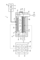
- FIG. 1 is a system configuration diagram illustrating an example of a substrate processing system according to an embodiment of the present disclosure.
- FIG. 2 is a schematic cross-sectional view showing an example of a structure of a PM according to an embodiment of the present disclosure.
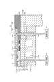
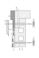
- FIG. 3 is an enlarged cross-sectional view showing an example of a structure in the vicinity of an edge of an electrostatic chuck.
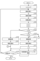
- FIG. 4 is a flow chart showing an example of a substrate processing method.
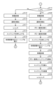
- FIG. 5 is a flow chart showing an example of a substrate processing method.
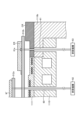
- FIG. 6 is a diagram showing an example of the position of the edge ring during cleaning.
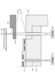
- FIG. 7 is a diagram showing an example of a process of carrying in a dummy substrate.
- FIG. 1 is a system configuration diagram illustrating an example of a substrate processing system according to an embodiment of the present disclosure.
- FIG. 2 is a schematic cross-sectional view showing an example of a structure of a PM according to an embodiment of the present disclosure.
- FIG. 3
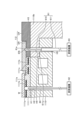
- FIG. 8 is a diagram showing an example of the position of the edge ring during cleaning.
- 9A to 9C are diagrams showing another example of the process of unloading the dummy substrate and the edge ring.
- FIG. 10 is a plan view showing an example of the positional relationship between the dummy substrate and the edge ring and the first and second forks.
- FIG. 11 is an enlarged cross-sectional view showing another example of a structure in the vicinity of the edge of an electrostatic chuck.
- FIG. 12 is a diagram showing an example of the positions of the edge ring and the covering ring during cleaning.
- the present disclosure therefore provides a technique that can more efficiently remove deposits that adhere to the edge ring.
- FIG. 1 is a system configuration diagram showing an example of a substrate processing system 50 according to an embodiment of the present disclosure.
- the substrate processing system 50 includes a VTM (Vacuum Transfer Module) 51, a storage device 52, a plurality of LLMs (Load Lock Modules) 53, an EFEM (Equipment Front End Module) 54, a plurality of PMs (Process Modules) 1, and a control unit 2.
- a plurality of PMs 1 are connected to a side wall of the VTM 51 via a gate valve G1. In the example of FIG. 1, six PMs 1 are connected to the VTM 51, but the number of PMs 1 connected to the VTM 51 may be more than six or less than six.
- the VTM 51 is an example of a vacuum transfer device.
- the storage device 52 is an example of a ring stocker.
- the PM 1 is an example of a plasma processing device. That is, the substrate processing system 50 includes the VTM 51, a plurality of PMs 1 connected to the VTM 51, the storage device 52 connected to the VTM 51, and a control unit 2.
- Each PM1 performs processes such as plasma etching and film formation on the substrate W to be processed.
- a plurality of LLMs 53 are connected to the other side wall of the VTM 51 via gate valves G2. In the example of FIG. 1, two LLMs 53 are connected to the VTM 51, but the number of LLMs 53 connected to the VTM 51 may be more than two, or may be just one.
- a transport robot 510 is disposed within the VTM 51.
- the transport robot 510 is an example of a transport device.
- the transport robot 510 has an arm 511 and a fork 512.
- the fork 512 is provided at the tip of the arm 511.
- a substrate W, an edge ring, and a dummy substrate are placed on the fork 512.
- the dummy substrate is an example of a cleaning substrate.
- the transport robot 510 transports the substrate W between the PM1 and another PM1, and between the PM1 and the LLM 53.
- the transport robot 510 also transports the edge ring and the dummy substrate between the PM1 and the storage device 52.
- a predetermined pressure atmosphere lower than atmospheric pressure is maintained within the VTM 51.
- each LLM 53 is connected to the VTM 51 via gate valve G2, and the other side wall is connected to the EFEM 54 via gate valve G3.
- the gate valve G3 is closed and the pressure inside the LLM 53 is reduced to a pressure equivalent to that inside the VTM 51.
- the gate valve G2 is opened and the substrate W in the LLM 53 is loaded into the VTM 51 by the transport robot 510.
- the transfer robot 510 transfers the substrate W from the VTM 51 into the LLM 53 via the gate valve G2, which is then closed.
- the pressure inside the LLM 53 is then raised to approximately the same as the pressure inside the EFEM 54.
- the gate valve G3 is then opened, and the substrate W inside the LLM 53 is transferred into the EFEM 54.
- Each load port 55 is connected to a container such as a FOUP (Front Opening Unified Pod) capable of accommodating multiple substrates W.
- the EFEM 54 may also be provided with an aligner module or the like that changes the orientation of the substrates W.
- the inside of the EFEM 54 is, for example, atmospheric pressure.
- a transport robot 540 is provided in the EFEM 54.
- the transport robot 540 moves inside the EFEM 54 along a guide rail 541 provided in the EFEM 54, and transports the substrate W between the LLM 53 and a container connected to the load port 55.
- An FFU (Fan Filter Unit) or the like is provided at the top of the EFEM 54, and dry air from which particles and the like have been removed is supplied from the top into the EFEM 54, forming a downflow in the EFEM 54.
- the inside of the EFEM 54 is atmospheric pressure, but in another embodiment, the pressure in the EFEM 54 may be controlled to be positive pressure. This makes it possible to suppress the intrusion of particles and the like into the EFEM 54 from the outside.
- the other side wall of the VTM 51 is connected to a storage device 52 via a gate valve G4.
- the storage device 52 stores an edge ring and a dummy substrate.
- the storage device 52 stores a replacement edge ring, a used edge ring, and a dummy substrate.
- the storage device 52 has a function of switching the pressure inside the storage device 52 between atmospheric pressure and a pressure approximately equal to that inside the VTM 51.
- the replacement edge ring may be a new edge ring, or it may be a used edge ring with a small amount of wear.
- the gate valve G4 is opened, and the transport robot 510 transports the used edge ring from the storage device 52 into the storage device 52 via the VTM 51. Then, the transport robot 510 transports a replacement edge ring from the storage device 52 into the PM1 via the VTM 51. Then, the gate valve G4 is closed, and the pressure inside the storage device 52 is switched from approximately the same as inside the VTM 51 to atmospheric pressure, after which the gate valve G5 is opened, and the used edge ring is transported outside the storage device 52 via the gate valve G5. Then, the replacement edge ring is transported into the storage device 52 via the gate valve G5.
- the gate valve G4 is opened, and the dummy substrate is carried into PM1 via the VTM 51 by the transport robot 510. Then, after cleaning inside PM1 is completed, the dummy substrate is returned to the accommodation device 52 by the transport robot 510.
- the dummy substrate is replaced, for example, the pressure inside the accommodation device 52 is switched from approximately the same as inside the VTM 51 to atmospheric pressure, and then the gate valve G5 is opened, and the dummy substrate is carried out to the outside of the accommodation device 52 via the gate valve G5. Then, a replacement dummy substrate is carried into the accommodation device 52 via the gate valve G5.
- the replacement dummy substrate may be a new dummy substrate, or may be a used dummy substrate with a small amount of wear.
- the control unit 2 processes computer-executable instructions that cause the substrate processing system 50 to perform the various steps described in this disclosure.
- the control unit 2 may be configured to control each element of the substrate processing system 50 to perform the various steps described herein. In one embodiment, a part or all of the control unit 2 may be included in the substrate processing system 50.
- the control unit 2 may include a processing unit 2a1, a storage unit 2a2, and a communication interface 2a3.
- the control unit 2 is realized, for example, by a computer 2a.
- the processing unit 2a1 may be configured to perform various control operations by reading a program from the storage unit 2a2 and executing the read program. This program may be stored in the storage unit 2a2 in advance, or may be acquired via a medium when necessary.
- the acquired program is stored in the storage unit 2a2 and is read from the storage unit 2a2 by the processing unit 2a1 and executed.
- the medium may be various storage media readable by the computer 2a, or may be a communication line connected to the communication interface 2a3.
- the processing unit 2a1 may be a CPU (Central Processing Unit).
- the memory unit 2a2 may include a RAM (Random Access Memory), a ROM (Read Only Memory), a HDD (Hard Disk Drive), an SSD (Solid State Drive), or a combination of these.
- the communication interface 2a3 may communicate with the substrate processing system 50 via a communication line such as a LAN (Local Area Network).
- FIG. 2 is a schematic cross-sectional view showing an example of the structure of PM1 in one embodiment of the present disclosure.
- PM1 is an example of a substrate processing apparatus.
- PM1 is a capacitively coupled plasma processing apparatus.
- PM1 includes a plasma processing chamber 10, a gas supply unit 20, a power supply 30, and an exhaust system 40.
- PM1 also includes a substrate support unit 11 and a gas inlet unit.
- the plasma processing chamber 10 is an example of a processing vessel.
- the gas inlet unit is configured to introduce at least one processing gas into the plasma processing chamber 10.
- the gas inlet unit includes a shower head 13.
- the substrate support unit 11 is disposed in the plasma processing chamber 10.
- the shower head 13 is disposed above the substrate support unit 11. In one embodiment, the shower head 13 constitutes at least a part of the ceiling of the plasma processing chamber 10.
- the plasma processing chamber 10 has a plasma processing space 10s defined by the shower head 13, a sidewall 10a of the plasma processing chamber 10, and the substrate support unit 11.
- the plasma processing chamber 10 has at least one gas supply port for supplying at least one processing gas to the plasma processing space 10s and at least one gas exhaust port for exhausting gas from the plasma processing space.
- the plasma processing chamber 10 is grounded.
- the shower head 13 and the substrate support 11 are electrically insulated from the housing of the plasma processing chamber 10.
- An opening 10b is formed in the sidewall 10a of the plasma processing chamber 10 for loading and unloading a substrate W into and from the plasma processing chamber 10.
- the opening 10b is opened and closed by a gate valve G1.
- the substrate support 11 includes a main body 111 and a ring assembly 112.
- the main body 111 is an example of a stage.
- the main body 111 has a central region 111a for supporting the substrate W and an annular region 111b for supporting the ring assembly 112.
- the central region 111a is an example of a first mounting surface
- the annular region 111b is an example of a second mounting surface.
- a wafer is an example of a substrate W.
- the annular region 111b of the main body 111 surrounds the central region 111a of the main body 111 in a plan view.
- the substrate W is disposed on the central region 111a of the main body 111, and the ring assembly 112 is disposed on the annular region 111b of the main body 111 so as to surround the substrate W on the central region 111a of the main body 111. Therefore, the central region 111a is also called a substrate support surface for supporting the substrate W, and the annular region 111b is also called a ring support surface for supporting the ring assembly 112.
- the main body 111 includes a base 1110 and an electrostatic chuck 1111.
- the base 1110 includes a conductive member.
- the conductive member of the base 1110 may function as a lower electrode.
- the electrostatic chuck 1111 is disposed on the base 1110.
- the electrostatic chuck 1111 includes a ceramic member 1111a and a first electrode 1111b disposed within the ceramic member 1111a.
- the ceramic member 1111a has a central region 111a. In one embodiment, the ceramic member 1111a also has an annular region 111b. Note that other members surrounding the electrostatic chuck 1111, such as an annular electrostatic chuck or an annular insulating member, may have the annular region 111b.
- the ring assembly 112 may be disposed on the annular electrostatic chuck or the annular insulating member, or may be disposed on both the electrostatic chuck 1111 and the annular insulating member.
- at least one RF/DC electrode coupled to an RF (Radio Frequency) power source 31 and/or a DC (Direct Current) power source 32, which will be described later, may be disposed within the ceramic member 1111a.
- the at least one RF/DC electrode functions as a lower electrode.
- the RF/DC electrode is also called a bias electrode.
- the conductive member of the base 1110 and the at least one RF/DC electrode may function as multiple lower electrodes.
- the first electrode 1111b may function as a lower electrode.
- the substrate support 11 includes at least one lower electrode.
- the ring assembly 112 includes one or more annular members.
- the one or more annular members include one or more edge rings and at least one cover ring.
- the edge rings are formed of a conductive or insulating material, and the cover rings are formed of an insulating material.
- the substrate support 11 may also include a temperature adjustment module configured to adjust at least one of the electrostatic chuck 1111, the ring assembly 112, and the substrate to a target temperature.
- the temperature adjustment module may include a heater, a heat transfer medium, a flow path 1110a, or a combination thereof.
- a heat transfer fluid such as brine or gas flows through the flow path 1110a.
- the flow path 1110a is formed in the base 1110, and one or more heaters are disposed in the ceramic member 1111a of the electrostatic chuck 1111.
- the substrate support 11 may also include a heat transfer gas supply unit configured to supply a heat transfer gas to a gap between the back surface of the substrate W and the central region 111a. Although omitted in FIG. 2, the substrate support 11 is provided with a plurality of lifter pins.
- the shower head 13 is configured to introduce at least one processing gas from the gas supply unit 20 into the plasma processing space 10s.
- the shower head 13 has at least one gas supply port 13a, at least one gas diffusion chamber 13b, and multiple gas inlets 13c.
- the processing gas supplied to the gas supply port 13a passes through the gas diffusion chamber 13b and is introduced into the plasma processing space 10s from the multiple gas inlets 13c.
- the shower head 13 also includes at least one upper electrode.
- the gas introduction unit may include, in addition to the shower head 13, one or more side gas injectors (SGIs) attached to one or more openings formed in the sidewall 10a.
- SGIs side gas injectors
- the gas supply 20 may include at least one gas source 21 and at least one flow controller 22.
- the gas supply 20 is configured to supply at least one process gas from a respective gas source 21 through a respective flow controller 22 to the showerhead 13.
- Each flow controller 22 may include, for example, a mass flow controller or a pressure-controlled flow controller.
- the gas supply 20 may include one or more flow modulation devices to modulate or pulse the flow rate of the at least one process gas.
- the power supply 30 includes an RF power supply 31 coupled to the plasma processing chamber 10 via at least one impedance matching circuit.
- the RF power supply 31 is configured to supply at least one RF signal (RF power) to at least one lower electrode and/or at least one upper electrode. This causes a plasma to be formed from at least one processing gas supplied to the plasma processing space 10s.
- the RF power supply 31 can function as at least a part of a plasma generating unit configured to generate plasma from one or more processing gases in the plasma processing chamber 10.
- a bias RF signal to the at least one lower electrode, a bias potential is generated on the substrate W, and ion components in the formed plasma can be attracted to the substrate W.
- the RF power supply 31 includes a first RF generating unit 31a and a second RF generating unit 31b.
- the first RF generating unit 31a is coupled to at least one lower electrode and/or at least one upper electrode via at least one impedance matching circuit and configured to generate a source RF signal (source RF power) for plasma generation.
- the source RF signal has a frequency in the range of 10 MHz to 150 MHz.
- the first RF generating unit 31a may be configured to generate multiple source RF signals having different frequencies. The generated one or more source RF signals are supplied to at least one lower electrode and/or at least one upper electrode.
- the second RF generator 31b is coupled to at least one lower electrode via at least one impedance matching circuit and configured to generate a bias RF signal (bias RF power).
- the frequency of the bias RF signal may be the same as or different from the frequency of the source RF signal.
- the bias RF signal has a frequency lower than the frequency of the source RF signal.
- the bias RF signal has a frequency in the range of 100 kHz to 60 MHz.
- the second RF generator 31b may be configured to generate multiple bias RF signals having different frequencies.
- the generated one or more bias RF signals are provided to at least one lower electrode. Also, in various embodiments, at least one of the source RF signal and the bias RF signal may be pulsed.
- the power supply 30 may also include a DC power supply 32 coupled to the plasma processing chamber 10.
- the DC power supply 32 includes a first DC generator 32a and a second DC generator 32b.
- the first DC generator 32a is connected to at least one lower electrode and configured to generate a first DC signal.
- the generated first bias DC signal is applied to the at least one lower electrode.
- the second DC generator 32b is connected to at least one upper electrode and configured to generate a second DC signal.
- the generated second DC signal is applied to the at least one upper electrode.
- At least one of the first and second DC signals may be pulsed.
- a sequence of voltage pulses is applied to at least one lower electrode and/or at least one upper electrode.
- the voltage pulses may have a rectangular, trapezoidal, triangular or combination thereof pulse waveform.
- a waveform generator for generating a sequence of voltage pulses from the DC signal is connected between the first DC generator 32a and at least one lower electrode.
- the first DC generator 32a and the waveform generator constitute a voltage pulse generator.
- the second DC generator 32b and the waveform generator constitute a voltage pulse generator
- the voltage pulse generator is connected to at least one upper electrode.
- the voltage pulses may have a positive polarity or a negative polarity.
- the sequence of voltage pulses may also include one or more positive polarity voltage pulses and one or more negative polarity voltage pulses within one period.
- the first and second DC generating units 32a and 32b may be provided in addition to the RF power source 31, or the first DC generating unit 32a may be provided in place of the second RF generating unit 31b.
- the exhaust system 40 may be connected to, for example, a gas exhaust port 10e provided at the bottom of the plasma processing chamber 10.
- the exhaust system 40 may include a pressure regulating valve and a vacuum pump. The pressure in the plasma processing space 10s is adjusted by the pressure regulating valve.
- the vacuum pump may include a turbomolecular pump, a dry pump, or a combination thereof.
- Figure 3 is an enlarged cross-sectional view showing an example of a structure near the edge of the electrostatic chuck 1111.
- the base 1110 is supported by an insulating member 1110b formed in a ring shape.
- the insulating member 1110b is included in the main body 111. That is, the main body 111 as a stage includes the base 1110, the electrostatic chuck 1111, and the insulating member 1110b.
- the ring assembly 112 has an edge ring ER and a cover ring CR. A portion of the edge ring ER is disposed on the annular region 111b.
- the outer periphery of the edge ring ER and the inner periphery of the cover ring CR overlap in a top view.
- the edge ring ER is formed of a conductive material such as silicon or silicon carbide.
- the cover ring CR is disposed on the insulating member 1110b.
- the cover ring CR is formed of an insulating material such as quartz, and protects the upper surface of the insulating member 1110b from plasma.
- the upper surface of the insulating member 1110b is an example of a third mounting surface.
- the edge ring ER may be made of an insulating material such as quartz.
- the cover ring CR may be made of a conductive material such as silicon or silicon carbide.
- a first electrode 1111b is embedded below the central region 111a, and a second electrode 1111c is embedded below the annular region 111b.
- the first electrode 1111b attracts the substrate W or a dummy substrate to the central region 111a by electrostatic force generated in response to an applied voltage.
- the second electrode 1111c attracts the edge ring ER to the annular region 111b by electrostatic force generated in response to an applied voltage.
- the first electrode 1111b is a monopolar electrode, but as another example, the first electrode 1111b may be a bipolar electrode.
- the second electrode 1111c is a bipolar electrode, but as another example, the second electrode 1111c may be a monopolar electrode.
- a through hole H1 is formed in the electrostatic chuck 1111, and a through hole H2 is formed in the base 1110.
- Lifter pins 60 are inserted into the through holes H1 and H2.
- the lifter pins 60 are raised and lowered by a lifting mechanism 62.
- the substrate W or dummy substrate placed on the central region 111a can be raised and lowered.
- three lifter pins 60 are provided in the central region 111a.
- a through hole H3 is formed in the cover ring CR, a through hole H4 is formed in the insulating member 1110b, and a through hole H5 is formed in the base 1110.
- Lifter pins 61 are inserted into the through holes H3 to H5.
- the lifter pins 61 are raised and lowered by the lifting mechanism 63.
- the edge ring ER on the cover ring CR can be raised and lowered by the lifter pins 61 being raised and lowered.
- three lifter pins 61 are provided in the annular region 111b.
- a recess ERr is formed on the lower surface of the edge ring ER corresponding to the position of the through hole H3, and when the lifter pins 61 are raised, the tip 61a of the lifter pins 61 abuts against the recess ERr. As a result, the lifter pins 61 can stably support the edge ring ER with their tips 61a.
- the lifting mechanism 63 is an example of a lifter.
- FIGS 4 and 5 are flow charts showing an example of a substrate processing method. Each step illustrated in Figures 4 and 5 is realized by the control unit 2 controlling each part of the substrate processing system 50.
- the substrate processing method illustrated in Figures 4 and 5 is an example of a cleaning method.
- n a is a variable for counting the number of times that the substrate W is processed before cleaning is performed without lifting the edge ring ER.
- n b is a variable for counting the number of times that the substrate W is processed before cleaning is performed with the edge ring ER lifted.
- n c is a variable for counting the number of times that the substrate W is processed before the edge ring ER is replaced.
- step S101 the gate valve G1 is opened, and the substrate W is loaded into PM1 by the transport robot 510.
- the lifter pins 60 are raised from the central region 111a of the electrostatic chuck 1111, and the substrate W is transferred to the lifter pins 60.
- the lifting mechanism 62 is then driven to lower the lifter pins 60, and the substrate W is placed on the central region 111a of the electrostatic chuck 1111.
- step S102 the substrate W is attracted to the central region 111a (S102).
- step S102 the substrate W is attracted and held in the central region 111a by electrostatic force generated in response to the voltage applied to the first electrode 1111b.
- a process such as plasma etching is performed on the substrate W (S103).
- Step S103 is an example of process a).
- the variables n a , n b , and n c are each incremented by 1 (S104). Then, it is determined whether the value of the variable n a is equal to or greater than a predetermined value N a (S105).
- the value of N a is, for example, 10.
- the value of N a is an example of the second number.
- step S106 the charge removal process of the substrate W is performed (S106).
- a predetermined gas e.g., nitrogen gas
- the inside of the plasma processing chamber 10 is controlled to a predetermined pressure.
- a voltage of a different polarity from the voltage applied to the first electrode 1111b is applied to the first electrode 1111b for a predetermined time, and then the application of the voltage to the first electrode 1111b is stopped. This allows the charge accumulated on the substrate W to escape via the gas in the plasma processing chamber 10.
- a predetermined gas e.g., nitrogen gas
- the inside of the plasma processing chamber 10 is controlled to a predetermined pressure
- RF power for plasma generation is supplied to the lower electrode or the upper electrode to generate plasma.
- a voltage of a polarity different from that applied to the first electrode 1111b is applied for a predetermined time, and then the application of the voltage to the first electrode 1111b is stopped, and the supply of RF power for generating plasma is also stopped. This allows the charge accumulated on the substrate W to be released via the plasma in the plasma processing chamber 10.
- step S107 the lifting mechanism 62 is driven to raise the lifter pins 60, thereby lifting the substrate W. Then, the gate valve G1 is opened, and the substrate W is removed from the PM1 by the transport robot 510.
- step S101 is executed again. If the processing of the substrate W is to be ended (S108: Yes), the substrate processing method shown in this flowchart ends.
- N b is, for example, 100.
- the value of N b is an example of a first number.
- step S110 charge elimination is performed on the substrate W by the same procedure as in step S106. Then, the substrate W after the process is unloaded (S111). Then, the value of the variable n a is initialized to 0 (S112).
- Step S113 is an example of process e), and the cleaning performed in step S113 is an example of the third cleaning.
- step S113 cleaning is performed inside the plasma processing chamber 10 with the edge ring ER placed on the annular region 111b.
- step S113 a cleaning gas is supplied into the plasma processing chamber 10, and cleaning is performed inside the plasma processing chamber 10 by plasma generated from the cleaning gas. Then, the process shown in step S108 is performed.
- the cleaning gas supplied into the plasma processing chamber 10 in step S113 includes at least one gas selected from the group consisting of O2 gas, CO gas, CO2 gas, COS gas, N2 gas, and H2 gas.
- the cleaning gas may further include a halogen-containing gas such as CF4 gas, NF3 gas, Cl2 gas, or HBr gas.
- step S115 the application of the voltage to the first electrode 1111b and the second electrode 1111c is stopped, and, for example, a predetermined gas (for example, nitrogen gas) is supplied at a predetermined flow rate into the plasma processing chamber 10, and the inside of the plasma processing chamber 10 is controlled to a predetermined pressure.
- a predetermined gas for example, nitrogen gas
- step S115 the discharge processing of the substrate W and the discharge processing of the edge ring ER are performed simultaneously.
- the discharge processing of the edge ring ER may be performed after the discharge processing of the substrate W is performed and the substrate W is unloaded.
- the processed substrate W is unloaded (S116), and the values of variables n a and n b are initialized to 0 (S117).
- the edge ring ER is lifted (S118).
- step S118 for example, as shown in FIG. 6, the lifter pins 61 are raised by driving the lifting mechanism 63, thereby lifting the edge ring ER and separating it from the annular region 111b.
- step S118 the height from the annular region 111b to the bottom surface of the edge ring ER is defined as h1.
- step S119 cleaning of the inside of the plasma processing chamber 10 is performed with the edge ring ER separated from the annular region 111b.
- step S119 a cleaning gas is supplied into the plasma processing chamber 10, and the inside of the plasma processing chamber 10 is cleaned by plasma generated from the cleaning gas. This makes it possible to efficiently remove deposits attached to the lower surface of the edge ring ER, the inner periphery of the edge ring ER, the annular region 111b, and the outer periphery of the central region 111a (the sidewall between the central region 111a and the annular region 111b). Then, the process shown in step S108 is performed.
- the cleaning gas supplied into the plasma processing chamber 10 in step S119 may be the same as or different from the cleaning gas supplied into the plasma processing chamber 10 in step S113.
- Step S119 is an example of process b), and the cleaning performed in step S119 is an example of the first cleaning.
- the processing conditions for the cleaning in step S119 include parameters consisting of gas type, gas flow ratio, gas flow rate, pressure, bias power, plasma generation power, and temperature of the mounting table.
- cleaning of the plasma processing chamber 10 is performed with the edge ring ER lifted up, not only immediately before replacing the edge ring ER, but also each time processing of a predetermined number of substrates W is completed. This makes it possible to remove deposits adhering to the edge ring ER before they build up to an amount that cannot be removed by cleaning. This makes it possible to more efficiently remove deposits adhering to the edge ring ER.
- n c is equal to or greater than the value of N c (S114: Yes)
- a charge removal process is performed on the substrate W and the edge ring ER (S120).
- charge is removed from the substrate W and the edge ring ER by a procedure similar to that of step S115. Then, the processed substrate W is unloaded (S121).
- step S122 the gate valve G4 is opened, and the dummy substrate is removed from the accommodation device 52 by the transport robot 510. Then, the gate valve G1 is opened, and the dummy substrate W' is loaded into the PM1 and transferred to the lifter pins 60, for example, as shown in FIG. 7. The lifting mechanism 62 is driven to lower the lifter pins 60, and the dummy substrate W' is placed on the central region 111a of the electrostatic chuck 1111.
- the diameter R1 of the dummy substrate W' is shorter than the inner diameter R2 of the edge ring ER, as shown in FIG. 7, for example. Therefore, even when the dummy substrate W' is placed on the central region 111a, the edge ring ER can be lifted without interference between the dummy substrate W' and the edge ring ER.
- the dummy substrate W' is attracted to the central region 111a (S123). Then, the edge ring ER is lifted (S124). In step S124, the lifter pins 61 are raised by driving the lifting mechanism 63, and the edge ring ER is lifted and separated from the annular region 111b, for example, as shown in FIG. 8.
- the height h2 from the annular region 111b to the bottom surface of the edge ring ER in step S124 is different from the height h1 from the annular region 111b to the bottom surface of the edge ring ER in step S118. For example, the height h2 is lower than the height h1.
- the height h2 and the height h1 may be the same height, or the height h2 may be greater than the height h1.
- Step S125 is an example of process c), and the cleaning performed in step S125 is an example of the second cleaning.
- the dummy substrate W' is placed in the central region 111a, and the edge ring ER is separated from the annular region 111b, and cleaning is performed in the plasma processing chamber 10.
- step S124 a cleaning gas is supplied into the plasma processing chamber 10, and cleaning is performed in the plasma processing chamber 10 by plasma generated from the cleaning gas.
- the cleaning gas supplied into the plasma processing chamber 10 in step S124 may be the same as or different from the cleaning gas supplied into the plasma processing chamber 10 in step S113 or S119.
- the processing conditions for cleaning in step S125 include parameters consisting of gas type, gas flow ratio, gas flow rate, pressure, bias power, plasma generation power, and temperature of the mounting table.
- the process conditions for cleaning in step S125 may be the process conditions for cleaning in step S119 with at least one parameter changed.
- the process conditions for cleaning in steps S125 and S119 include at least one parameter selected from the group of parameters consisting of gas type, gas flow ratio, gas flow rate, pressure, bias power, plasma generation power, temperature of electrostatic chuck 1111, and cleaning time.
- step S125 it is preferable that cleaning is performed under conditions with higher cleaning performance than the cleaning performed in step S119. This allows the deposits attached to the edge ring ER after use to be sufficiently removed, and prevents the deposits from falling during the transportation process of the edge ring ER after use.
- the plasma generation power supplied to the upper electrode and/or the lower electrode in the cleaning in step S125 may be greater than the plasma generation power supplied in the first cleaning. Therefore, PM1 further includes at least one first RF generating unit 31a. The first plasma is generated by a first source RF power from the at least one first RF generating unit 31a, and the second plasma is generated by a second source RF power from the at least one first RF generating unit 31a.
- the second source RF power is greater than the first source RF power.
- the cleaning in step S125 may be performed with a bias power greater than that in the cleaning in step S119.
- no bias power may be provided in the cleaning in step S119, and bias power may be provided in the cleaning in step S125.
- PM1 includes at least one bias electrode disposed in the substrate support 11 and at least one second RF generator 31b.
- the at least one second RF generator 31b is configured to provide a first bias RF power to the at least one bias electrode in the first cleaning and a second bias RF power to the at least one bias electrode in the second cleaning.
- the second bias RF power is greater than the first bias RF power.
- the first bias RF power has a zero power level.
- PM1 may include at least one voltage pulse generator.
- the at least one voltage pulse generator is configured to provide a sequence of a plurality of first voltage pulses to the at least one bias electrode in the first cleaning and a sequence of a plurality of second voltage pulses to the at least one bias electrode in the second cleaning.
- the first voltage pulse has a first voltage level
- the second voltage pulse has a second voltage level.
- the second voltage pulse is greater than the first voltage level.
- the first voltage level has a zero voltage level.
- the cleaning in step S125 may be performed at a higher pressure than the cleaning in step S119.
- the first cleaning is performed at a first pressure
- the second cleaning is performed at a second pressure greater than the first pressure.
- the cleaning in step S125 may be performed at a higher pressure and with a higher bias power than the cleaning in step S119.
- the temperature of the electrostatic chuck 1111 in the cleaning in step S125 may be higher than the temperature of the electrostatic chuck 1111 in the cleaning in step S119.
- the PM1 further includes a temperature adjustment module.
- the temperature control module is configured to maintain the substrate support 11 at a first temperature in the first cleaning, and to maintain the substrate support 11 at a second temperature higher than the first temperature in the second cleaning.
- the cleaning in step S125 may be performed for a longer time than the cleaning in step S119.
- the cleaning in step S125 may be performed using a gas (e.g., a halogen-containing gas) that is more corrosive than the gas used in the cleaning performed in step S119.
- the cleaning in step S119 may also use a gas (e.g., a halogen-containing gas), and the flow rate of the corrosive gas in the cleaning in step S125 may be higher than the flow rate of the corrosive gas in the cleaning in step S119.
- the step S125 is performed with a dummy substrate W' placed on the central region 111a. This can reduce damage to the central region 111a even when the inside of the plasma processing chamber 10 is cleaned under conditions with high cleaning performance. Alternatively, the cleaning performed in step S125 may be performed without the dummy substrate W' being placed in the central region 111a.
- step S126 discharge is performed on the dummy substrate W' (S126).
- step S126 discharge is performed on the substrate W using the same procedure as in step 106.
- the dummy substrate W' and the edge ring ER are removed (S127).
- step S127 the lifting mechanism 62 is driven to raise the lifter pins 60, thereby lifting the dummy substrate W'.
- the gate valve G1 is opened, and the dummy substrate W' is removed from PM1 by the transport robot 510 and returned to the accommodation device 52.
- the edge ring ER is removed from PM1 by the transport robot 510 and transported into the accommodation device 52.
- Step S127 is an example of process d).
- a replacement edge ring ER is carried into PM1 (S128).
- the transfer robot 510 carries the replacement edge ring ER out of the storage device 52, and the replacement edge ring ER is carried into PM1.
- an edge ring ER that has been used but has a small amount of wear may be carried into PM1.
- step S129 the replacement edge ring ER is attracted to the annular region 111b (S129).
- step S129 the edge ring ER is attracted and held to the annular region 111b by electrostatic force generated in response to the voltage applied to the second electrode 1111c.
- the values of variables n a , n b , and n c are initialized to 0 (S130), and the process shown in step S108 is executed. Note that after step S129, a process for adjusting the condition inside the plasma processing chamber 10, such as seasoning, may be executed.
- the substrate processing apparatus (PM1) in this embodiment includes a processing container (plasma processing chamber 10), a stage (main body 111), an edge ring ER, a lifter (lifting mechanism 63), and a controller 2.
- the stage is provided in the processing container and has a first placement surface (central region 111a) on which a substrate W is placed, and a second placement surface (111b) surrounding the outer periphery of the first placement surface.
- the edge ring ER is configured to be placed on the second placement surface.
- the lifter raises and lowers the edge ring ER relative to the second placement surface.
- the controller 2 is configured to execute steps a), b), and c).
- step a) the controller 2 performs plasma processing on the substrate W placed on the first placement surface. Furthermore, in step b), the control unit 2 controls the lifter to separate the edge ring ER from the second mounting surface and performs a first cleaning inside the processing vessel every time step a) is performed on a predetermined first number (N b ) of substrates W. Furthermore, in step c), the control unit 2 controls the lifter to separate the edge ring ER from the second mounting surface and performs a second cleaning inside the processing vessel before replacing the edge ring ER. That is, the control unit 2 is configured to control each element of the substrate processing system 50 to perform the following steps.
- step f) controlling each element of PM1 to perform plasma processing on substrates W on the substrate mounting surface; b) performing step a) on a first number of substrates W; c) after step b), controlling at least one lifting mechanism 63 to lift the edge ring ER with a plurality of lifter pins 61 relative to the ring mounting surface; d) in the state of step c), controlling each element of PM1 to perform a first cleaning with a first plasma generated from a first cleaning gas in the plasma processing chamber 10; e) performing step a) on a second number of substrates W greater than the first number; f) after step e), controlling each element of the substrate processing system 50 to lift the edge ring ER with a plurality of lifter pins 61 relative to the ring mounting surface; and g) in the state of step f), controlling each element of PM1 to perform a second cleaning with a second plasma generated from a second cleaning gas in the plasma processing chamber 10.
- the processing conditions in the second cleaning may be modified by changing at least one parameter from the processing conditions in the first cleaning.
- the processing conditions in the first cleaning and the second cleaning may include at least one parameter selected from the group of parameters consisting of gas type, gas flow ratio, gas flow rate, pressure, bias power, plasma generation power, stage temperature, and cleaning time.
- the second cleaning may be performed with a plasma generation power higher than that of the first cleaning.
- bias power may not be supplied in the first cleaning, and bias power may be supplied in the second cleaning.
- the second cleaning may be performed with a pressure higher than that of the first cleaning.
- the second cleaning may be performed with a bias power higher than that of the first cleaning.
- the stage temperature in the second cleaning may be higher than the stage temperature in the first cleaning.
- the cleaning time in the second cleaning may be longer than the cleaning time in the first cleaning. This allows for efficient removal of deposits attached to the bottom surface of the edge ring ER, the inner periphery of the edge ring ER, the annular region 111b, and the outer periphery of the central region 111a (the sidewall between the central region 111a and the annular region 111b). Therefore, when replacing the edge ring ER, generation of particles due to deposits from the edge ring ER after use can be suppressed.
- the second cleaning is performed with the dummy substrate W' placed on the first placement surface. This makes it possible to reduce damage to the central region 111a caused by cleaning.
- the height h1 from the second mounting surface to the edge ring ER when the first cleaning is performed and the height h2 from the second mounting surface to the edge ring ER when the second cleaning is performed may be different.
- the height h2 may be lower than the height h1. This can increase the density of the plasma around the edge ring ER, improving the cleaning ability in the second cleaning.
- control unit 2 is further configured to perform step e).
- step e) a third cleaning is performed in the processing vessel with the edge ring ER placed on the second placement surface.
- Step e) is performed every time step a) is performed on a second number (N a ) of substrates W that is smaller than the first number. This makes it possible to reduce deposits in the processing vessel.
- a first electrode 1111b is embedded inside the stage corresponding to the first placement surface
- a second electrode 1111c is embedded inside the stage corresponding to the second placement surface.
- the substrate W is attracted to the first placement surface by electrostatic force generated by a voltage applied to the first electrode 1111b.
- the edge ring ER is attracted to the second placement surface by electrostatic force generated by a voltage applied to the second electrode 1111c.
- the control unit 2 is configured to perform a discharge process on the edge ring ER at the same timing as the discharge process performed on the substrate W for which the process of step a) has been completed, before steps b) and c) are performed. This allows the processing time to be reduced compared to when the discharge process on the substrate W and the discharge process on the edge ring ER are performed at different times.
- the inside of the processing vessel is cleaned using plasma generated from a cleaning gas containing at least one gas selected from the group consisting of O2 gas, CO gas, CO2 gas, COS gas, N2 gas, and H2 gas.
- a cleaning gas containing at least one gas selected from the group consisting of O2 gas, CO gas, CO2 gas, COS gas, N2 gas, and H2 gas.
- a halogen-containing gas such as CF4 gas, NF3 gas, Cl2 gas, or HBr gas may be further supplied into the processing vessel.
- a halogen-containing gas may be further supplied into the processing vessel, and the flow rate of the halogen-containing gas supplied into the processing vessel in the second cleaning may be greater than the flow rate of the halogen-containing gas supplied into the processing vessel in the first cleaning. This allows the deposits adhering to the edge ring ER to be removed more efficiently.
- the substrate processing system 50 in this embodiment includes a vacuum transport device (VTM 51) configured to transport the substrate W in a vacuum environment, a substrate processing device (PM1) configured to process the substrate W, and a storage device 52 configured to store a dummy substrate W'.
- the substrate processing device includes a processing vessel, a stage, an edge ring ER, a lifting mechanism 63, and a control unit 2.
- the stage is provided in the processing vessel and has a first mounting surface on which the substrate W is placed and a second mounting surface surrounding the outer periphery of the first mounting surface.
- the edge ring ER is formed in an annular shape and is configured to be placed on the second mounting surface.
- the lifting mechanism 63 raises and lowers the edge ring ER relative to the second mounting surface.
- the control unit 2 is configured to execute steps a), b), and c).
- step a) the control unit 2 performs plasma processing on the substrate W placed on the first mounting surface.
- step b) the control unit 2 performs a first cleaning in the processing vessel in a state in which the edge ring ER is separated from the second mounting surface by controlling the lifting mechanism 63 each time step a) is performed on a predetermined first number of substrates W.
- step c) the control unit 2 performs a second cleaning in the processing vessel in a state in which the edge ring ER is separated from the second mounting surface by controlling the lifting mechanism 63 before replacing the edge ring ER.
- a dummy substrate is transported from the accommodation device into the processing vessel, and the second cleaning is performed in a state in which the dummy substrate W' is placed on the first mounting surface. This allows the deposits attached to the edge ring ER to be removed more efficiently.
- the storage device 52 also stores a replacement edge ring ER. This makes it possible to reduce the storage space for the dummy substrate W' and the edge ring ER.
- the cleaning method in this embodiment also includes steps a), c), and d).
- step a) plasma processing is performed on a substrate placed on a first placement surface of a stage provided in a processing vessel.
- step b) a first cleaning is performed in the processing vessel in a state in which an edge ring, which is placed on a second placement surface of the stage surrounding the outer periphery of the first placement surface and is arranged to surround the substrate W placed on the first placement surface, is separated from the second placement surface by a lifting mechanism.
- step c) a second cleaning is performed in the processing vessel in a state in which the edge ring ER is separated from the second placement surface before replacing the edge ring ER.
- Step b) is performed every time step a) is performed on a predetermined first number of substrates W. This makes it possible to more efficiently remove deposits attached to the edge ring ER.
- steps S113 and S119 cleaning is performed without placing a dummy substrate W' in the central region 111a, but the disclosed technology is not limited to this.
- steps S113 and S119 cleaning may be performed with a dummy substrate W' placed in the central region 111a. This can reduce damage to the central region 111a of the electrostatic chuck 1111 during cleaning.
- step S127 the edge ring ER is removed after the dummy substrate W' is removed, but the disclosed technology is not limited to this.
- the dummy substrate W' may be removed after the edge ring ER is removed. This makes it possible to prevent deposits from falling from the edge ring ER onto the central region 111a when the edge ring ER is removed.
- the replacement edge ring ER is brought in in step S128, but the disclosed technology is not limited to this.
- the replacement edge ring ER may be brought in and then the dummy substrate W' may be removed. This makes it possible to prevent particles and the like adhering to the replacement edge ring ER from falling onto the central region 111a.
- step S127 in the above embodiment the used edge ring ER is unloaded after the dummy substrate W' is unloaded, but the disclosed technology is not limited to this.
- a transport robot 510 having a first fork 512a and a second fork 512b on an arm 511 may be used to unload the dummy substrate W' and the edge ring ER at the same time.
- the dummy substrate W' is supported by the first fork 512a provided above
- the edge ring ER is supported by the second fork 512b provided below. This can reduce the time required to unload the dummy substrate W' and the edge ring ER.
- the edge ring ER may be supported by the first fork 512a provided above, and the dummy substrate W' may be supported by the second fork 512b provided below.
- FIG. 11 is an enlarged cross-sectional view showing another example of the structure near the edge of the electrostatic chuck 1111.
- the lifter pin 61 includes an upper portion 610 and a lower portion 611 that is thicker than the upper portion 610.
- the upper portion 610 is thinner than the inner diameter of the through holes H3 to H5.
- the lower portion 611 is thinner than the inner diameter of the through holes H4 and H5, but thicker than the inner diameter of the through hole H3.
- the edge ring ER is an example of a first ring.
- the cover ring CR is an example of a second ring.
- the lifting mechanism 63 is an example of at least one actuator.
- the PM1 includes a plasma processing chamber 10, a substrate support 11, a first ring ER, a second ring CR, a plurality of lifter pins 61, and at least one lifting mechanism 63.
- the substrate support 11 is disposed in the plasma processing chamber 10 and has a substrate mounting surface, a first ring mounting surface, and a second ring mounting surface.
- the first ring ER is disposed to surround the substrate W on the substrate mounting surface and has an inner annular portion and an outer annular portion.
- the inner annular portion of the first ring ER is mounted on the first ring mounting surface.
- the second ring CR has an inner annular portion and an outer annular portion.
- the inner annular portion of the second ring CR is configured to support the outer annular portion of the first ring ER, and the outer annular portion of the second ring CR is mounted on the second ring mounting surface.
- the inner annular portion of the second ring CR has a plurality of through holes H3.
- the plurality of lifter pins 61 are aligned with the plurality of through holes H3, respectively.
- Each lifter pin 61 has an upper portion 610 and a lower portion 611. The upper portion 610 of the lifter pin 61 is configured to support the first ring ER through the corresponding through hole H3.
- the horizontal dimension of the upper portion 610 of the lifter pin 61 is smaller than the horizontal dimension of the corresponding through hole H3, and the horizontal dimension of the lower portion 611 of the lifter pin 61 is larger than the horizontal dimension of the corresponding through hole H3.
- At least one lifting mechanism 63 moves the plurality of lifter pins 61 vertically.
- the upper portion 610 is longer than h1. Therefore, when the lifter pins 61 rise, the lifter pins 61 can lift only the edge ring ER to a height h1. When the lifter pins 61 further rise, the upper end surface 611a of the lower portion 611 can further lift the covering ring CR, as shown in FIG. 12, for example. In step S125, the edge ring ER and the covering ring CR are lifted to the state shown in FIG. 12 and cleaning is performed, so that the deposits attached to the lower surface of the covering ring CR and the upper surface of the insulating member 1110b can also be efficiently removed.
- control unit 2 is configured to control each element of the substrate processing system 50 to execute the following steps.
- step a) controlling each element of PM1 to perform plasma processing on substrates W on the substrate mounting surface; b) performing step a) on a first number of substrates W; c) after step b), controlling at least one lifting mechanism 63 to lift the first ring ER with the multiple lifter pins 61 relative to the first ring mounting surface; d) in the state of step c), controlling each element of PM1 to perform a first cleaning with a first plasma generated from a first cleaning gas in the plasma processing chamber 10; e) performing step a) on a second number of substrates W greater than the first number; f) after step e), controlling each element of the substrate processing system 50 to place a cleaning substrate W' on the substrate mounting surface and control at least one lifting mechanism 63 to lift the first ring ER with the multiple lifter pins 61 relative to the first ring mounting surface.
- step f controlling each element of PM1 to perform a second cleaning using a second plasma generated from a second cleaning gas in the plasma processing chamber 10; and h) controlling each element of the substrate processing system 50 to transport the first ring ER from the plasma processing chamber 10 to the accommodation device 52 in order to replace the first ring ER.
- the first cleaning is performed with the substrate mounting surface exposed (i.e., waferless), and the first cleaning gas includes at least one selected from the group consisting of O2 gas, CO gas, CO2 gas, COS gas, N2 gas, and H2 gas.
- the second cleaning gas includes a halogen-containing gas.
- the halogen-containing gas includes a CF-containing gas, NF3 gas, Cl2 gas, or HBr gas.
- the CF-containing gas includes CF4 gas.
- the cleaning substrate W' has an outer diameter smaller than an inner diameter of the first ring ER.
- the first ring ER is lifted to a first height in step c) and is lifted to a second height different from the first height in step f).
- the controller 2 is configured to control each element of the substrate processing system 50 to further perform the following steps.
- step i) performing step a) on a third number of substrates W greater than the second number; j) after step i), controlling each element of the substrate processing system 50 to place a cleaning substrate W' on the substrate mounting surface and controlling at least one lifting mechanism 63 to lift the second ring CR with the lifter pins 61 relative to the second ring mounting surface; k) in the state of step j), controlling each element of PM1 to perform a third cleaning using a third plasma generated from a third cleaning gas in the plasma processing chamber 10; l) controlling each element of the substrate processing system 50 to transport the second ring CR from the plasma processing chamber 10 to the accommodation device 52 in order to replace the second ring CR.
- control unit 2 may be configured to control each element of the substrate processing system 50 to perform the following steps. i) performing step a) on a third number of substrates W greater than the second number; j) after step i), controlling each element of the substrate processing system 50 to place a cleaning substrate W' on the substrate mounting surface and controlling at least one lifting mechanism 63 to lift the first ring ER with the upper part 610 of the lifter pins 61 relative to the first ring mounting surface and lift the second ring CR with the lower part 611 of the lifter pins 61 relative to the second ring mounting surface; k) in the state of step j), controlling each element of PM1 to perform a third cleaning using a third plasma generated from a third cleaning gas in the plasma processing chamber; l) transporting the first ring ER and the second ring CR from the plasma processing chamber 10 to the accommodation device 52 in order to exchange the first ring ER and the second ring CR.
- the third cleaning gas is the same as
- the dummy substrate W' is accommodated in a storage device 52 separate from the VTM 51, but the disclosed technology is not limited to this.
- the dummy substrate W' may be accommodated in a space provided in the VTM 51.
- a replacement edge ring ER may also be accommodated in this space.
- the dummy substrate W' may be accommodated in a container such as a FOUP connected to the load port 55.
- the PM1 is used as an example to perform processing on the substrate W using plasma, but the disclosed technology is not limited to this.
- the disclosed technology can also be applied to devices that do not use plasma, so long as the device performs processing on the substrate W, such as film formation or heat treatment.
- a capacitively coupled plasma has been described as an example of a plasma source used for PM1, but the plasma source is not limited to this.
- plasma sources other than capacitively coupled plasma include inductively coupled plasma (ICP), microwave excited surface wave plasma (SWP), electron cyclotron resonance plasma (ECP), and helicon wave excited plasma (HWP).
- ICP inductively coupled plasma
- SWP microwave excited surface wave plasma
- ECP electron cyclotron resonance plasma
- HWP helicon wave excited plasma
- the microwaves used in microwave excited surface wave plasma (SWP) are an example of electromagnetic waves.
- a processing vessel A processing vessel; a stage provided in the processing chamber and having a first mounting surface on which a substrate is placed and a second mounting surface surrounding an outer periphery of the first mounting surface; an edge ring configured to be placed on the second mounting surface; a lifter configured to raise and lower the edge ring relative to the second mounting surface; and A control unit.
- the control unit is a) performing a plasma treatment on the substrate placed on the first placement surface; b) every time step a) is performed on a predetermined first number of the substrates, controlling the lifter to separate the edge ring from the second mounting surface and perform a first cleaning inside the processing vessel; c) before replacing the edge ring, controlling the lifter to move the edge ring away from the second mounting surface and performing a second cleaning inside the processing vessel.
- Appendix 2 2.
- processing conditions in the first cleaning and the second cleaning include at least one parameter selected from the group of parameters consisting of a gas type, a gas flow ratio, a gas flow rate, a pressure, a bias power, a plasma generating power, a temperature of the stage, and a cleaning time.
- processing conditions in the first cleaning and the second cleaning include at least one parameter selected from the group of parameters consisting of a gas type, a gas flow ratio, a gas flow rate, a pressure, a bias power, a plasma generating power, a temperature of the stage, and a cleaning time.
- a plasma generating power supplied in the second cleaning is greater than a plasma generating power supplied in the first cleaning.
- the second cleaning is performed with a bias power larger than that of the first cleaning.
- Appendix 6 6.
- the substrate processing apparatus wherein a bias power is not supplied in the first cleaning and a bias power is supplied in the second cleaning.
- Appendix 7 The substrate processing apparatus according to claim 1, wherein the second cleaning is performed at a pressure higher than that of the first cleaning.
- Appendix 8 8. The substrate processing apparatus according to claim 1, wherein a temperature of the stage in the second cleaning is higher than a temperature of the stage in the first cleaning.
- Appendix 9 9. The substrate processing apparatus according to claim 1, wherein the cleaning time in the second cleaning is longer than the cleaning time in the first cleaning. (Appendix 10) 10. The substrate processing apparatus according to claim 1, wherein the second cleaning is performed in a state where a dummy substrate is placed on the first placement surface.
- control unit is e) performing a third cleaning of the inside of the processing vessel while the edge ring is placed on the second placement surface; 14.
- a first electrode is embedded inside the stage corresponding to the first mounting surface, a second electrode is embedded inside the stage corresponding to the second mounting surface, the substrate is attracted to the first placement surface by electrostatic force generated by a voltage applied to the first electrode; the edge ring is attracted to the second mounting surface by an electrostatic force generated by a voltage applied to the second electrode;
- the control unit is A substrate processing apparatus as described in any one of appendices 1 to 14, which is configured to perform a discharge process on the edge ring at the same timing as the discharge process performed on the substrate after the processing of step a) is completed before the processing of steps b) and c) is performed.
- the substrate processing apparatus according to claim 1, wherein in the first cleaning and the second cleaning, cleaning inside the processing vessel is performed using plasma generated from a cleaning gas including at least one selected from the group consisting of O gas, CO gas, CO gas, COS gas, N gas, and H gas.
- a cleaning gas including at least one selected from the group consisting of O gas, CO gas, CO gas, COS gas, N gas, and H gas.
- Appendix 18 18.
- a halogen-containing gas is further supplied into the processing vessel; 19.
- the substrate processing apparatus of claim 18, wherein a flow rate of the halogen-containing gas supplied into the processing vessel in the second cleaning is greater than a flow rate of the halogen-containing gas supplied into the processing vessel in the first cleaning.
- the substrate processing apparatus includes: A processing vessel; a stage provided within the processing chamber, the stage having a first mounting surface on which the substrate is mounted and a second mounting surface surrounding an outer periphery of the first mounting surface and on which an edge ring is mounted; an edge ring configured to be placed on the second mounting surface; a lifter configured to raise and lower the edge ring relative to the second mounting surface; and and a control unit.
- the control unit is a) performing a plasma treatment on the substrate placed on the first placement surface; b) every time step a) is performed on a predetermined first number of the substrates, controlling the lifter to separate the edge ring from the second mounting surface and perform a first cleaning inside the processing vessel; c) before replacing the edge ring, controlling the lifter to separate the edge ring from the second mounting surface and performing a second cleaning of the inside of the processing vessel; In the second cleaning, the dummy substrate is transferred from the accommodation device into the processing vessel, and the second cleaning is performed in a state in which the dummy substrate is placed on the first placement surface. (Appendix 22) 22. The substrate processing system of claim 21, wherein the edge ring is also accommodated in the accommodation device.
- a transfer device configured to transfer the edge ring and the dummy substrate is provided within the vacuum transfer device; 23.
- (Appendix 24) a) performing a plasma processing on a substrate placed on a first mounting surface of a stage provided in a processing chamber; b) moving an edge ring, which is placed on a second mounting surface of the stage surrounding an outer periphery of the first mounting surface and is arranged to surround the substrate placed on the first mounting surface, away from the second mounting surface by a lifter, and performing a first cleaning inside the processing vessel; c) before replacing the edge ring, moving the edge ring away from the second mounting surface and performing a second cleaning inside the processing vessel; The cleaning method, wherein the step b) is performed every time the step a) is performed on a predetermined first number of the substrates.
- Plasma processing chamber 11 Substrate support unit 111 Main body unit 1110 Base 1111 Electrostatic chuck 1111a Ceramic member 1111b First electrode 1111c Second electrode 112 Ring assembly 13 Shower head 20 Gas supply unit 21 Gas source 22 Flow rate controller 30 Power supply 31 RF power supply 32 DC power supply 40 Exhaust system 50 Substrate processing system 51 VTM 510 Transport robot 511 Arm 512 Fork 512a First fork 512b Second fork 52 Storage device 53 LLM 54 EFEM 540: Transport robot 541: Guide rail 55: Load port 60: Lifter pin 61: Lifter pin 610: Upper portion 611: Lower portion 61a: Tip 62: Lifting mechanism 63: Lifting mechanism
Landscapes
- Engineering & Computer Science (AREA)
- Physics & Mathematics (AREA)
- Plasma & Fusion (AREA)
- Chemical & Material Sciences (AREA)
- Analytical Chemistry (AREA)
- Health & Medical Sciences (AREA)
- Epidemiology (AREA)
- Public Health (AREA)
- Drying Of Semiconductors (AREA)
- Container, Conveyance, Adherence, Positioning, Of Wafer (AREA)
- Robotics (AREA)
- Cleaning Or Drying Semiconductors (AREA)
Priority Applications (4)
| Application Number | Priority Date | Filing Date | Title |
|---|---|---|---|
| CN202380043422.4A CN119301743A (zh) | 2022-10-31 | 2023-10-25 | 基板处理装置、基板处理系统以及清洁方法 |
| JP2024554424A JPWO2024095840A1 (cg-RX-API-DMAC7.html) | 2022-10-31 | 2023-10-25 | |
| KR1020247039829A KR20250100582A (ko) | 2022-10-31 | 2023-10-25 | 기판 처리 장치, 기판 처리 시스템 및 클리닝 방법 |
| US18/980,363 US20250112031A1 (en) | 2022-10-31 | 2024-12-13 | Substrate processing apparatus, substrate processing system, and cleaning method |
Applications Claiming Priority (2)
| Application Number | Priority Date | Filing Date | Title |
|---|---|---|---|
| JP2022174530 | 2022-10-31 | ||
| JP2022-174530 | 2022-10-31 |
Related Child Applications (1)
| Application Number | Title | Priority Date | Filing Date |
|---|---|---|---|
| US18/980,363 Continuation US20250112031A1 (en) | 2022-10-31 | 2024-12-13 | Substrate processing apparatus, substrate processing system, and cleaning method |
Publications (1)
| Publication Number | Publication Date |
|---|---|
| WO2024095840A1 true WO2024095840A1 (ja) | 2024-05-10 |
Family
ID=90930291
Family Applications (1)
| Application Number | Title | Priority Date | Filing Date |
|---|---|---|---|
| PCT/JP2023/038415 Ceased WO2024095840A1 (ja) | 2022-10-31 | 2023-10-25 | 基板処理装置、基板処理システム、およびクリーニング方法 |
Country Status (6)
| Country | Link |
|---|---|
| US (1) | US20250112031A1 (cg-RX-API-DMAC7.html) |
| JP (1) | JPWO2024095840A1 (cg-RX-API-DMAC7.html) |
| KR (1) | KR20250100582A (cg-RX-API-DMAC7.html) |
| CN (1) | CN119301743A (cg-RX-API-DMAC7.html) |
| TW (1) | TW202437382A (cg-RX-API-DMAC7.html) |
| WO (1) | WO2024095840A1 (cg-RX-API-DMAC7.html) |
Cited By (1)
| Publication number | Priority date | Publication date | Assignee | Title |
|---|---|---|---|---|
| WO2026042625A1 (ja) * | 2024-08-22 | 2026-02-26 | 東京エレクトロン株式会社 | 処理装置、クリーニング方法、および静電チャック |
Families Citing this family (1)
| Publication number | Priority date | Publication date | Assignee | Title |
|---|---|---|---|---|
| JPWO2023042804A1 (cg-RX-API-DMAC7.html) * | 2021-09-14 | 2023-03-23 |
Citations (2)
| Publication number | Priority date | Publication date | Assignee | Title |
|---|---|---|---|---|
| JP2014127627A (ja) * | 2012-12-27 | 2014-07-07 | Tokyo Electron Ltd | 薄膜形成装置の洗浄方法、薄膜形成方法、薄膜形成装置、及び、プログラム |
| JP2021141308A (ja) * | 2020-03-02 | 2021-09-16 | 東京エレクトロン株式会社 | クリーニング方法およびプラズマ処理装置 |
Family Cites Families (3)
| Publication number | Priority date | Publication date | Assignee | Title |
|---|---|---|---|---|
| JP6635888B2 (ja) | 2016-07-14 | 2020-01-29 | 東京エレクトロン株式会社 | プラズマ処理システム |
| TW202605992A (zh) * | 2019-09-26 | 2026-02-01 | 日商東京威力科創股份有限公司 | 基板支持器及電漿處理裝置 |
| US11804368B2 (en) * | 2020-03-02 | 2023-10-31 | Tokyo Electron Limited | Cleaning method and plasma processing apparatus |
-
2023
- 2023-10-25 JP JP2024554424A patent/JPWO2024095840A1/ja active Pending
- 2023-10-25 KR KR1020247039829A patent/KR20250100582A/ko active Pending
- 2023-10-25 WO PCT/JP2023/038415 patent/WO2024095840A1/ja not_active Ceased
- 2023-10-25 CN CN202380043422.4A patent/CN119301743A/zh active Pending
- 2023-10-30 TW TW112141484A patent/TW202437382A/zh unknown
-
2024
- 2024-12-13 US US18/980,363 patent/US20250112031A1/en active Pending
Patent Citations (2)
| Publication number | Priority date | Publication date | Assignee | Title |
|---|---|---|---|---|
| JP2014127627A (ja) * | 2012-12-27 | 2014-07-07 | Tokyo Electron Ltd | 薄膜形成装置の洗浄方法、薄膜形成方法、薄膜形成装置、及び、プログラム |
| JP2021141308A (ja) * | 2020-03-02 | 2021-09-16 | 東京エレクトロン株式会社 | クリーニング方法およびプラズマ処理装置 |
Cited By (1)
| Publication number | Priority date | Publication date | Assignee | Title |
|---|---|---|---|---|
| WO2026042625A1 (ja) * | 2024-08-22 | 2026-02-26 | 東京エレクトロン株式会社 | 処理装置、クリーニング方法、および静電チャック |
Also Published As
| Publication number | Publication date |
|---|---|
| US20250112031A1 (en) | 2025-04-03 |
| KR20250100582A (ko) | 2025-07-03 |
| JPWO2024095840A1 (cg-RX-API-DMAC7.html) | 2024-05-10 |
| CN119301743A (zh) | 2025-01-10 |
| TW202437382A (zh) | 2024-09-16 |
Similar Documents
| Publication | Publication Date | Title |
|---|---|---|
| JP7515383B2 (ja) | クリーニング方法およびプラズマ処理装置 | |
| JP2020115541A (ja) | ウェハエッジプラズマシース調整機能を備える半導体プラズマ処理装置 | |
| US20250112031A1 (en) | Substrate processing apparatus, substrate processing system, and cleaning method | |
| CN115398603B (zh) | 等离子处理装置以及等离子处理方法 | |
| US11887824B2 (en) | Method of cleaning plasma processing apparatus and plasma processing apparatus | |
| US12444583B2 (en) | Electrostatic attraction method and plasma processing apparatus | |
| JP2024014768A (ja) | 基板搬送システムおよび搬送モジュール | |
| JP2025108733A (ja) | 基板処理装置、基板処理方法、および半導体装置の製造方法 | |
| TW202141620A (zh) | 清洗方法及半導體裝置之製造方法 | |
| US20240222095A1 (en) | Plasma processing apparatus and plasma processing method | |
| TW202503955A (zh) | 叢集工具 | |
| JP7715467B2 (ja) | 基板処理装置及びリング部材の位置合わせ方法 | |
| JP2023038801A (ja) | 基板処理方法 | |
| US20240347325A1 (en) | Plasma processing apparatus | |
| US12531213B2 (en) | Plasma processing apparatus | |
| JP2025034857A (ja) | 基板処理装置およびクリーニング方法 | |
| JP3225695U (ja) | ウェハエッジプラズマシース調整機能を備える半導体プラズマ処理装置 | |
| JP2025024972A (ja) | 基板処理方法及び基板処理装置 | |
| TW202603947A (zh) | 搬運系統 | |
| JP2024092751A (ja) | 基板保持方法および基板処理システム | |
| JP2025090149A (ja) | プラズマ処理方法及びプラズマ処理装置 | |
| JP2024098708A (ja) | プラズマ処理装置 | |
| JP2023140638A (ja) | 裏面加工装置、プラズマ処理システム及び基板処理方法 | |
| WO2023148861A1 (ja) | プラズマ処理装置のクリーニング方法 | |
| WO2025004821A1 (ja) | 運搬装置、基板の搬送方法、および処理システム |
Legal Events
| Date | Code | Title | Description |
|---|---|---|---|
| 121 | Ep: the epo has been informed by wipo that ep was designated in this application |
Ref document number: 23885598 Country of ref document: EP Kind code of ref document: A1 |
|
| ENP | Entry into the national phase |
Ref document number: 2024554424 Country of ref document: JP Kind code of ref document: A |
|
| WWE | Wipo information: entry into national phase |
Ref document number: 202380043422.4 Country of ref document: CN |
|
| WWP | Wipo information: published in national office |
Ref document number: 202380043422.4 Country of ref document: CN |
|
| NENP | Non-entry into the national phase |
Ref country code: DE |
|
| WWP | Wipo information: published in national office |
Ref document number: 1020247039829 Country of ref document: KR |
|
| 122 | Ep: pct application non-entry in european phase |
Ref document number: 23885598 Country of ref document: EP Kind code of ref document: A1 |