WO2024084905A1 - 窒化物半導体装置 - Google Patents
窒化物半導体装置 Download PDFInfo
- Publication number
- WO2024084905A1 WO2024084905A1 PCT/JP2023/034856 JP2023034856W WO2024084905A1 WO 2024084905 A1 WO2024084905 A1 WO 2024084905A1 JP 2023034856 W JP2023034856 W JP 2023034856W WO 2024084905 A1 WO2024084905 A1 WO 2024084905A1
- Authority
- WO
- WIPO (PCT)
- Prior art keywords
- layer
- nitride semiconductor
- gan
- algan
- semiconductor layer
- Prior art date
- Legal status (The legal status is an assumption and is not a legal conclusion. Google has not performed a legal analysis and makes no representation as to the accuracy of the status listed.)
- Ceased
Links
Images




Classifications
-
- H—ELECTRICITY
- H10—SEMICONDUCTOR DEVICES; ELECTRIC SOLID-STATE DEVICES NOT OTHERWISE PROVIDED FOR
- H10D—INORGANIC ELECTRIC SEMICONDUCTOR DEVICES
- H10D30/00—Field-effect transistors [FET]
- H10D30/01—Manufacture or treatment
- H10D30/061—Manufacture or treatment of FETs having Schottky gates
-
- H—ELECTRICITY
- H10—SEMICONDUCTOR DEVICES; ELECTRIC SOLID-STATE DEVICES NOT OTHERWISE PROVIDED FOR
- H10D—INORGANIC ELECTRIC SEMICONDUCTOR DEVICES
- H10D30/00—Field-effect transistors [FET]
- H10D30/40—FETs having zero-dimensional [0D], one-dimensional [1D] or two-dimensional [2D] charge carrier gas channels
- H10D30/47—FETs having zero-dimensional [0D], one-dimensional [1D] or two-dimensional [2D] charge carrier gas channels having two-dimensional [2D] charge carrier gas channels, e.g. nanoribbon FETs or high electron mobility transistors [HEMT]
- H10D30/471—High electron mobility transistors [HEMT] or high hole mobility transistors [HHMT]
- H10D30/475—High electron mobility transistors [HEMT] or high hole mobility transistors [HHMT] having wider bandgap layer formed on top of lower bandgap active layer, e.g. undoped barrier HEMTs such as i-AlGaN/GaN HEMTs
-
- H—ELECTRICITY
- H10—SEMICONDUCTOR DEVICES; ELECTRIC SOLID-STATE DEVICES NOT OTHERWISE PROVIDED FOR
- H10D—INORGANIC ELECTRIC SEMICONDUCTOR DEVICES
- H10D30/00—Field-effect transistors [FET]
- H10D30/01—Manufacture or treatment
- H10D30/051—Manufacture or treatment of FETs having PN junction gates
-
- H—ELECTRICITY
- H10—SEMICONDUCTOR DEVICES; ELECTRIC SOLID-STATE DEVICES NOT OTHERWISE PROVIDED FOR
- H10D—INORGANIC ELECTRIC SEMICONDUCTOR DEVICES
- H10D30/00—Field-effect transistors [FET]
- H10D30/40—FETs having zero-dimensional [0D], one-dimensional [1D] or two-dimensional [2D] charge carrier gas channels
- H10D30/47—FETs having zero-dimensional [0D], one-dimensional [1D] or two-dimensional [2D] charge carrier gas channels having two-dimensional [2D] charge carrier gas channels, e.g. nanoribbon FETs or high electron mobility transistors [HEMT]
- H10D30/471—High electron mobility transistors [HEMT] or high hole mobility transistors [HHMT]
-
- H—ELECTRICITY
- H10—SEMICONDUCTOR DEVICES; ELECTRIC SOLID-STATE DEVICES NOT OTHERWISE PROVIDED FOR
- H10D—INORGANIC ELECTRIC SEMICONDUCTOR DEVICES
- H10D30/00—Field-effect transistors [FET]
- H10D30/80—FETs having rectifying junction gate electrodes
- H10D30/83—FETs having PN junction gate electrodes
-
- H—ELECTRICITY
- H10—SEMICONDUCTOR DEVICES; ELECTRIC SOLID-STATE DEVICES NOT OTHERWISE PROVIDED FOR
- H10D—INORGANIC ELECTRIC SEMICONDUCTOR DEVICES
- H10D30/00—Field-effect transistors [FET]
- H10D30/80—FETs having rectifying junction gate electrodes
- H10D30/87—FETs having Schottky gate electrodes, e.g. metal-semiconductor FETs [MESFET]
-
- H—ELECTRICITY
- H10—SEMICONDUCTOR DEVICES; ELECTRIC SOLID-STATE DEVICES NOT OTHERWISE PROVIDED FOR
- H10D—INORGANIC ELECTRIC SEMICONDUCTOR DEVICES
- H10D62/00—Semiconductor bodies, or regions thereof, of devices having potential barriers
- H10D62/10—Shapes, relative sizes or dispositions of the regions of the semiconductor bodies; Shapes of the semiconductor bodies
- H10D62/102—Constructional design considerations for preventing surface leakage or controlling electric field concentration
- H10D62/103—Constructional design considerations for preventing surface leakage or controlling electric field concentration for increasing or controlling the breakdown voltage of reverse-biased devices
-
- H—ELECTRICITY
- H10—SEMICONDUCTOR DEVICES; ELECTRIC SOLID-STATE DEVICES NOT OTHERWISE PROVIDED FOR
- H10D—INORGANIC ELECTRIC SEMICONDUCTOR DEVICES
- H10D62/00—Semiconductor bodies, or regions thereof, of devices having potential barriers
- H10D62/80—Semiconductor bodies, or regions thereof, of devices having potential barriers characterised by the materials
- H10D62/81—Semiconductor bodies, or regions thereof, of devices having potential barriers characterised by the materials of structures exhibiting quantum-confinement effects, e.g. single quantum wells; of structures having periodic or quasi-periodic potential variation
- H10D62/815—Semiconductor bodies, or regions thereof, of devices having potential barriers characterised by the materials of structures exhibiting quantum-confinement effects, e.g. single quantum wells; of structures having periodic or quasi-periodic potential variation of structures having periodic or quasi-periodic potential variation, e.g. superlattices or multiple quantum wells [MQW]
- H10D62/8171—Doping structures, e.g. doping superlattices or nipi superlattices
-
- H—ELECTRICITY
- H10—SEMICONDUCTOR DEVICES; ELECTRIC SOLID-STATE DEVICES NOT OTHERWISE PROVIDED FOR
- H10D—INORGANIC ELECTRIC SEMICONDUCTOR DEVICES
- H10D64/00—Electrodes of devices having potential barriers
- H10D64/111—Field plates
-
- H—ELECTRICITY
- H10—SEMICONDUCTOR DEVICES; ELECTRIC SOLID-STATE DEVICES NOT OTHERWISE PROVIDED FOR
- H10D—INORGANIC ELECTRIC SEMICONDUCTOR DEVICES
- H10D62/00—Semiconductor bodies, or regions thereof, of devices having potential barriers
- H10D62/80—Semiconductor bodies, or regions thereof, of devices having potential barriers characterised by the materials
- H10D62/83—Semiconductor bodies, or regions thereof, of devices having potential barriers characterised by the materials being Group IV materials, e.g. B-doped Si or undoped Ge
Definitions
- This disclosure relates to nitride semiconductor devices.
- Patent Document 1 describes an example of a normally-off type HEMT using a nitride semiconductor.
- a nitride semiconductor device includes a first nitride semiconductor layer, a second nitride semiconductor layer formed on the first nitride semiconductor layer and having a band gap larger than that of the first nitride semiconductor layer, and a gate electrode, a source electrode, and a drain electrode formed above the second nitride semiconductor layer.
- the first nitride semiconductor layer is a layer containing GaN.
- the half-width of an X-ray rocking curve for the (102) plane of the first nitride semiconductor layer is 1100 arcsec or more and 1400 arcsec or less.
- the nitride semiconductor device according to one embodiment can suppress an increase in on-resistance.
- FIG. 1 is a schematic cross-sectional view of an exemplary nitride semiconductor device according to one embodiment.
- FIG. 2 is a schematic cross-sectional view showing an exemplary structure of various nitride semiconductor layers formed on a semiconductor substrate in the nitride semiconductor device of FIG.
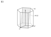
- FIG. 3 is a diagram showing a schematic view of the (102) plane of the first nitride semiconductor layer.
- FIG. 4 is a schematic diagram showing a screw dislocation.
- FIG. 5 is a diagram showing a schematic diagram of an edge dislocation.
- FIG. 6 is a graph showing the relationship between the XRC half-width and the on-resistance variation rate for the (102) plane of the first nitride semiconductor layer, measured for various nitride semiconductor devices including first nitride semiconductor layers having different crystal defect densities.
- nitride semiconductor device 10 is, for example, a HEMT using GaN.
- the nitride semiconductor device 10 includes a semiconductor substrate 12, a buffer layer 14 formed on the semiconductor substrate 12, a first nitride semiconductor layer 16 formed on the buffer layer 14, and a second nitride semiconductor layer 18 formed on the first nitride semiconductor layer 16.
- the semiconductor substrate 12 may be formed of silicon (Si), silicon carbide (SiC), GaN, sapphire, or other substrate materials.
- the semiconductor substrate 12 is a Si substrate.
- the thickness of the semiconductor substrate 12 may be, for example, 200 ⁇ m or more and 1500 ⁇ m or less.
- the Z-axis direction of the mutually orthogonal XYZ axes shown in FIG. 1 is a direction perpendicular to the main surface (top surface in FIG. 1) of the semiconductor substrate 12.
- the term "planar view" used in this specification refers to viewing the nitride semiconductor device 10 from above along the Z-axis direction, unless otherwise explicitly stated.
- the buffer layer 14 includes one or more nitride semiconductor layers.
- the buffer layer 14 may be made of any material that can suppress warping of the semiconductor substrate 12 and the occurrence of cracks in the nitride semiconductor device 10 due to a mismatch in the thermal expansion coefficient between the semiconductor substrate 12 and the first nitride semiconductor layer 16.
- the buffer layer 14 includes at least one of an aluminum nitride (AlN) layer, an aluminum gallium nitride (AlGaN) layer, and a graded AlGaN layer having different aluminum (Al) compositions.
- AlN aluminum nitride
- AlGaN aluminum gallium nitride
- AlGaN aluminum gallium nitride
- the buffer layer 14 may be composed of a single AlN layer, a single AlGaN layer, a layer having an AlGaN/GaN superlattice structure, a layer having an AlN/AlGaN superlattice structure, or a layer having an AlN/GaN superlattice structure. Exemplary structures of the buffer layer 14 are described below with reference to FIG. 2.
- the first nitride semiconductor layer 16 is a layer containing GaN.
- the first nitride semiconductor layer 16 includes a GaN composite layer in which a plurality of GaN layers are stacked.
- the thickness of the first nitride semiconductor layer 16 can be, for example, 0.5 ⁇ m or more and 2 ⁇ m or less. An exemplary structure of the first nitride semiconductor layer 16 will be described below with reference to FIG. 2.
- the second nitride semiconductor layer 18 is made of a nitride semiconductor having a larger band gap than the first nitride semiconductor layer 16.
- the second nitride semiconductor layer 18 may be, for example, an AlGaN layer. Since the band gap increases as the Al composition increases, the second nitride semiconductor layer 18, which is an AlGaN layer, has a larger band gap than the first nitride semiconductor layer 16 including a GaN composite layer.
- the second nitride semiconductor layer 18 is made of Al x Ga 1-x N, where x is 0.1 ⁇ x ⁇ 0.4, and more preferably 0.1 ⁇ x ⁇ 0.3.
- the thickness of the second nitride semiconductor layer 18 can be, for example, 5 nm or more and 20 nm or less.
- the first nitride semiconductor layer 16 and the second nitride semiconductor layer 18 are composed of nitride semiconductors having different lattice constants. Therefore, the nitride semiconductor (e.g., GaN) constituting the first nitride semiconductor layer 16 and the nitride semiconductor (e.g., AlGaN) constituting the second nitride semiconductor layer 18 form a lattice-mismatched heterojunction.
- the nitride semiconductor e.g., GaN
- the nitride semiconductor e.g., AlGaN
- the energy level of the conduction band of the first nitride semiconductor layer 16 near the heterojunction interface is lower than the Fermi level.
- a two-dimensional electron gas (2DEG) 20 spreads in the first nitride semiconductor layer 16 at a position close to the heterojunction interface between the first nitride semiconductor layer 16 and the second nitride semiconductor layer 18 (for example, within a range of about several nm from the interface).
- the nitride semiconductor device 10 includes a gate structure 22, a source electrode 24, and a drain electrode 26 formed on the second nitride semiconductor layer 18, and a passivation layer 28 formed on the second nitride semiconductor layer 18 and covering the gate structure 22.
- the passivation layer 28 includes a source side opening 28A and a drain side opening 28B that each expose a part of the upper surface of the second nitride semiconductor layer 18.
- the passivation layer 28 can be made of at least one of silicon nitride (SiN), silicon dioxide (SiO 2 ), silicon oxynitride (SiON), aluminum oxide (Al 2 O 3 ), AlN, and aluminum oxynitride (AlON), for example.
- the thickness of the passivation layer 28 can be, for example, 80 nm or more and 150 nm or less.
- the gate structure 22 includes a gate layer 30 and a gate electrode 32 formed on the gate layer 30.
- the gate layer 30 may be, for example, a GaN layer doped with acceptor-type impurities, i.e., a p-type GaN layer.
- the acceptor-type impurities may be, for example, at least one of zinc (Zn), magnesium (Mg), and carbon (C).
- the maximum concentration of the acceptor-type impurities in the gate layer 30 may be 7 ⁇ 10 18 cm ⁇ 3 or more and 1 ⁇ 10 20 cm ⁇ 3 or less.
- the gate layer 30 is located between the source side opening 28A and the drain side opening 28B of the passivation layer 28 in the X-axis direction shown in FIG. 1.
- the gate layer 30 is spaced apart from the source side opening 28A and the drain side opening 28B, and is located closer to the source side opening 28A than the drain side opening 28B.
- the gate electrode 32 includes one or more metal layers.
- the gate electrode 32 is formed, for example, by a titanium nitride (TiN) layer.
- the gate electrode 32 is formed by a first metal layer composed of Ti (titanium) and a second metal layer formed on the first metal layer and composed of TiN.
- the gate electrode 32 forms a Schottky junction with the gate layer 30.
- the thickness of the gate electrode 32 can be, for example, 50 nm or more and 200 nm or less.
- the source electrode 24 and the drain electrode 26 include one or more metal layers.
- the source electrode 24 and the drain electrode 26 may be formed by one or any combination of a Ti layer, a TiN layer, an Al layer, an AlSiCu layer, and an AlCu layer.
- At least a portion of the source electrode 24 is filled in the source side opening 28A and is in ohmic contact with the 2DEG 20 directly below the second nitride semiconductor layer 18 through the source side opening 28A.
- at least a portion of the drain electrode 26 is filled in the drain side opening 28B and is in ohmic contact with the 2DEG 20 directly below the second nitride semiconductor layer 18 through the drain side opening 28B.
- the semiconductor substrate 12 is connected to the source electrode 24, and a voltage having the same potential as the source electrode 24 is applied to the semiconductor substrate 12.
- the gate structure 22 includes a gate layer 30 and a gate electrode 32.
- the gate layer 30 includes a top surface on which the gate electrode 32 is located, and a bottom surface in contact with the second nitride semiconductor layer 18.
- the gate layer 30 includes a gate layer body 34 including the top surface of the gate layer 30, and a source side extension 36 and a drain side extension 38 each of which is thinner than the gate layer body 34.
- the gate layer body 34, the source side extension 36, and the drain side extension 38 are all in contact with the second nitride semiconductor layer 18.
- the source side extension 36 extends from the gate layer main body 34 toward the source side opening 28A.
- a passivation layer 28 exists between the source electrode 24 embedded in the source side opening 28A and the source side extension 36.
- the drain side extension 38 extends from the gate layer main body 34 toward the drain side opening 28B.
- a passivation layer 28 exists between the drain electrode 26 embedded in the drain side opening 28B and the drain side extension 38.
- the gate layer main body 34 is located between the source side extension 36 and the drain side extension 38, and is formed integrally with the source side extension 36 and the drain side extension 38.
- the gate layer main body 34 is formed to have a ridge-like (rectangular) cross section.
- the cross-sectional shape of the gate layer main body 34 is not particularly limited, and may be, for example, a trapezoidal cross section or another cross-sectional shape. Due to the presence of the source side extension 36 and the drain side extension 38, the bottom surface of the gate layer 30 has a larger area than the top surface of the gate layer 30.
- the drain side extension portion 38 extends further toward the outside of the gate layer main body portion 34 in a plan view than the source side extension portion 36. That is, the drain side extension portion 38 may have a dimension in the X-axis direction that is larger than that of the source side extension portion 36.
- the dimension (length) in the X-axis direction of the source side extension portion 36 may be, for example, 0.2 ⁇ m or more and 0.3 ⁇ m or less.
- the dimension (length) in the X-axis direction of the drain side extension portion 38 may be, for example, 0.2 ⁇ m or more and 0.6 ⁇ m or less.
- the gate layer body 34 corresponds to a relatively thick portion of the gate layer 30.
- the thickness of the gate layer body 34 can be, for example, 80 nm or more and 150 nm or less.
- the thickness of the gate layer body 34 can be determined taking into consideration various parameters including the gate threshold voltage.
- the source side extension 36 and the drain side extension 38 each have a thickness smaller than that of the gate layer body 34.
- the source side extension 36 and the drain side extension 38 each can have a thickness less than half that of the gate layer body 34.
- the source side extension 36 and the drain side extension 38 may each include a flat portion of approximately constant thickness.
- the thickness of the flat portion of the source side extension 36 and the flat portion of the drain side extension 38 may be, for example, 5 nm or more and 25 nm or less.
- approximately constant thickness refers to a thickness that is within the range of manufacturing variation (e.g., 20%).
- the source side extension 36 and the drain side extension 38 may each include an intermediate portion between the flat portion and the gate layer main body 34 that is thicker than the flat portion. In one example, the intermediate portion may have a thickness that gradually decreases the farther it is from the gate layer main body 34.
- a gate layer 30 containing acceptor-type impurities is provided directly under a gate electrode 32.
- a channel (current path) of the 2DEG 20 is formed in the region of the first nitride semiconductor layer 16 directly under the gate layer main body 34, thereby providing electrical continuity between the source and drain.
- the 2DEG 20 disappears in at least a part of the region of the first nitride semiconductor layer 16 directly under the gate layer main body 34 (see FIG. 1).
- the gate layer main body 34 contains acceptor-type impurities, which raises the energy levels of the first nitride semiconductor layer 16 and the second nitride semiconductor layer 18, thereby depleting the 2DEG 20.
- the nitride semiconductor device 10 is realized as a normally-off type HEMT.
- the nitride semiconductor device 10 includes a field plate electrode 40 formed on the passivation layer 28.
- the field plate electrode 40 is formed integrally with the source electrode 24, and covers the entire gate structure 22 in a plan view.
- the field plate electrode 40 can be considered as a part of the source electrode 24, and a voltage having the same potential as the source electrode 24 is applied to the field plate electrode 40.
- the field plate electrode 40 may be provided separately from the source electrode 24, and a control voltage other than the source voltage may be applied to the field plate electrode 40.
- the field plate electrode 40 is spaced apart from the drain electrode 26.
- the field plate electrode 40 includes an end 40A located between the gate layer 30 (drain side extension 38) and the drain electrode 26 (drain side opening 28B) in a planar view.
- the field plate electrode 40 serves to reduce electric field concentration near the end of the gate electrode 32 and near the end of the gate layer 30 when a drain voltage is applied to the drain electrode 26 in a zero bias state in which no gate input voltage is applied to the gate electrode 32.
- Exemplary Structures of Various Nitride Semiconductor Layers on a Semiconductor Substrate 2 is a schematic cross-sectional view showing an exemplary structure of various nitride semiconductor layers formed on the semiconductor substrate 12. As described above, the buffer layer 14, the first nitride semiconductor layer 16, the second nitride semiconductor layer 18, and the gate layer 30 (third nitride semiconductor layer) are formed in this order on the semiconductor substrate 12. Below, an exemplary structure of each layer will be described in order.
- the buffer layer 14 may include a first buffer layer 52 formed on the semiconductor substrate 12 and a second buffer layer 54 formed on the first buffer layer 52.
- the first buffer layer 52 may be, for example, an AlN layer.
- the thickness of the first buffer layer 52 may be, for example, not less than 100 nm and not more than 300 nm.
- the second buffer layer 54 may be, for example, an AlGaN composite layer in which multiple AlGaN layers are stacked.
- the second buffer layer 54 may be a graded AlGaN layer in which multiple AlGaN layers having different aluminum (Al) compositions are stacked.
- Al aluminum
- the second buffer layer 54 is formed as a graded AlGaN layer in which three AlGaN layers, namely, a first AlGaN layer 54A, a second AlGaN layer 54B, and a third AlGaN layer 54C, are stacked in that order.
- the thickness of each of the first to third AlGaN layers 54A, 54B, and 54C may be, for example, 100 nm or more and 300 nm or less.
- the third AlGaN layer 54C is located at the top of the second buffer layer 54 (buffer layer 14).
- the third AlGaN layer 54C may have a lower Al composition and a greater thickness than the second AlGaN layer 54B.
- the second AlGaN layer 54B may have a lower Al composition than the first AlGaN layer 54A and the same thickness as the first AlGaN layer 54A.
- the thicknesses of the first and second AlGaN layers 54A and 54B may each be about 100 nm
- the thickness of the third AlGaN layer 54C may be twice or more the thickness of the second AlGaN layer 54B, for example, 200 nm or more.
- the Al composition ratios in the first to third AlGaN layers 54A, 54B, and 54C may be approximately 80% ( ⁇ 5%), approximately 50% ( ⁇ 5%), and approximately 20% ( ⁇ 5%), respectively.
- the third AlGaN layer 54C has a different Al composition from the second AlGaN layer 54B (lower Al composition than the second AlGaN layer 54B in the example of FIG. 2), and is therefore grown in a distorted state with respect to the lattice constant of the second AlGaN layer 54B.
- the thickness of the third AlGaN layer 54C is greater than the thickness of the second AlGaN layer 54B. For this reason, the occurrence of lattice relaxation (dislocations) is promoted in the third AlGaN layer 54C so as to relieve the internal stress (distortion due to lattice mismatch) accumulated as distortion in the third AlGaN layer 54C.
- the third AlGaN layer 54C is configured to have a lower Al composition and a greater thickness than the second AlGaN layer 54B.
- the number of AlGaN layers forming the second buffer layer 54 and the thickness of each layer are adjusted to increase the crystal defect density of the buffer layer 14.
- the buffer layer 14 may contain an impurity that forms an acceptor level.
- the impurity in the buffer layer 14 may be, for example, at least one of carbon (C) and iron (Fe).
- the concentration of the impurity may be, for example, 4 ⁇ 10 16 cm ⁇ 3 or more.
- such an impurity may be introduced into a part of the buffer layer 14 to make the buffer layer 14 semi-insulating, thereby suppressing leakage current in the buffer layer 14 and improving the breakdown voltage.
- the impurity may be introduced only into the third AlGaN layer 54C, or only into the second and third AlGaN layers 54B and 54C.
- the impurity may be introduced into all of the first to third AlGaN layers 54A, 54B, and 54C of the second buffer layer 54.
- the layers doped with the impurity that forms the acceptor level among the first to third AlGaN layers 54A to 54C correspond to impurity-doped AlGaN layers.
- the first nitride semiconductor layer 16 may include a GaN composite layer in which a plurality of GaN layers are stacked.
- the GaN composite layer may be formed by stacking one or more impurity-doped GaN layers doped with impurities that form an acceptor level and non-doped GaN layers alternately.
- the uppermost layer of the GaN composite layer is a non-doped GaN layer.
- non-doped GaN layer used in this disclosure is defined as a GaN layer to which no impurities are intentionally introduced.
- the impurity in the impurity-doped GaN layer may be, for example, carbon (C).
- the concentration of the impurity in the impurity-doped GaN layer may be 5 ⁇ 10 17 cm ⁇ 3 or more and 5 ⁇ 10 19 cm ⁇ 3 or less.
- such an impurity is introduced into a part of the first nitride semiconductor layer 16 to make at least a part of the first nitride semiconductor layer 16 other than the surface region semi-insulating, thereby suppressing leakage current in the first nitride semiconductor layer 16 and improving the breakdown voltage.
- the first nitride semiconductor layer 16 is formed as a three-layer GaN composite layer in which three GaN layers, namely a first GaN layer 62, a second GaN layer 64, and a third GaN layer 66, are stacked in this order.
- the first GaN layer 62 is an undoped GaN layer
- the second GaN layer 64 is an impurity-doped GaN layer
- the third GaN layer 66 is an undoped GaN layer.
- the 2DEG 20 (see FIG. 1), which serves as the channel of the HEMT, is formed in the third GaN layer 66 located at the top of the GaN composite layer (first nitride semiconductor layer 16).
- the third GaN layer 66 in which the 2DEG 20 is generated is also functionally called an electron transport layer.
- the first to third GaN layers 62, 64, 66 may have the same thickness or different thicknesses.
- the thickness of the first GaN layer 62 may be, for example, 50 nm to 300 nm
- the thickness of the second GaN layer 64 may be, for example, 300 nm to 600 nm.
- the thickness of the third GaN layer 66 may be, for example, 200 nm to 500 nm.
- the thickness of the GaN composite layer, i.e., the entire first nitride semiconductor layer 16, may be, for example, 0.5 ⁇ m to 2 ⁇ m, as described above.
- the number and thickness of one or more impurity-doped GaN layers (the second GaN layer 64 in the example of FIG. 2) and/or the number and thickness of one or more non-doped GaN layers (the first GaN layer 62 and the third GaN layer 66 in the example of FIG. 2) are adjusted.
- the crystal defects are formed as a plurality of dislocations (threading dislocations) that extend linearly in the stacking direction across both the impurity-doped GaN layer and the non-doped GaN layer.
- the second nitride semiconductor layer 18 is an AlGaN layer, and the gate layer 30 is a p-type GaN layer.
- the second nitride semiconductor layer 18 is also functionally called an electron supply layer for the electron transit layer (third GaN layer 66) of the first nitride semiconductor layer 16.
- the nitride semiconductor device 10 is configured as a normally-off type HEMT as described above.
- the carrier (electron) concentration of the 2DEG 20 generated in the first nitride semiconductor layer 16 decreases. This increases the channel potential and therefore the on-resistance.
- electrons trapped in the deep acceptor level in the crystal are not easily released, so the on-resistance can remain high.
- Such deep acceptor levels can be formed, for example, by implanting impurities into the first nitride semiconductor layer 16 and/or the buffer layer 14.
- the first nitride semiconductor layer 16 is configured to maintain its crystal defect density within a predetermined range. Crystal defects caused by crystal distortion contribute to the formation of donor levels. From this perspective, the crystal defect density in the crystal of the first nitride semiconductor layer 16 and/or in the crystal of the buffer layer 14 is controlled to form a donor level that compensates for the acceptors.
- X-ray rocking curve (XRC) measurements are generally used to evaluate crystal defect density.
- the half-width of the XRC is used as an index value that quantifies the distortion of the crystal, and therefore correlates with the crystal defect density. More accurately, the half-width is the full width at half maximum (FWHM), but below it will simply be referred to as the half-width.
- the crystal defect density of the first nitride semiconductor layer 16 is controlled so that the XRC half-width for the (102) plane of the first nitride semiconductor layer 16 is 1100 arcsec or more and 1400 arcsec or less.
- the "XRC half-width for the (102) plane" of the first nitride semiconductor layer 16 may be simply referred to as the "(102) half-width.”
- FIG. 3 is a diagram showing a schematic diagram of the (102) plane of the first nitride semiconductor layer 16.
- the (102) plane of the first nitride semiconductor layer 16 is a crystal plane with Miller indices (102) in a hexagonal crystal that is a unit lattice of GaN forming the first nitride semiconductor layer 16, and corresponds to the crystal plane M102 of the hexagonal HC shown in FIG. 3.
- the X-ray rocking curve for the (102) plane refers to a rocking curve obtained by X-ray diffraction for the (102) plane.
- the types of crystal defects include screw dislocations and edge dislocations, which are lattice misalignments formed in the stacking direction of the crystal stacking structure.
- a screw dislocation is a dislocation that is formed at an angle to the direction perpendicular to the stacking plane of the crystal stacking structure, and is formed specifically by a tilt of the crystal axis of the crystal growth direction.
- An edge dislocation is a dislocation that is formed in the direction perpendicular to the stacking plane of the crystal stacking structure, and is formed specifically by a twist of the crystal axis within the plane.
- Fig. 4 is a schematic diagram of a screw dislocation
- Fig. 5 is a schematic diagram of an edge dislocation. Note that Figs. 4 and 5 show only one layer in a hexagonal crystal system having a crystal stacking structure in the X-axis direction, with Fig. 4 being a front view of a portion of the crystal structure, and Fig. 5 being a plan view of the crystal structure in Fig. 4.
- the screw dislocation is formed by the tilt of the c-axis C2 of the hexagonal crystal HC2 relative to the c-axis C1 of the hexagonal crystal HC1 (and the c-axis C4 of the hexagonal crystal HC4 in FIG. 5).
- a lattice misalignment D1 is formed between the hexagonal crystal HC2 and the hexagonal crystals HC1 and HC4, which is inclined with respect to the direction perpendicular to the stacking plane of the crystal stacking structure (Z-axis direction).
- This lattice misalignment D1 is carried over in the thickness direction (X-axis direction) of the first nitride semiconductor layer 16, resulting in the formation of a crystal defect (threading dislocation) due to the screw dislocation.
- edge dislocations are formed by twisting around the c-axis C3 of the hexagonal crystal HC3.
- This twisting around the c-axis C3 creates a lattice misalignment D2 between the hexagonal crystal HC3 and the hexagonal crystals HC1 and HC4 along the direction perpendicular to the stacking plane of the crystal stacking structure (Z-axis direction).
- This lattice misalignment D2 is carried over into the thickness direction (X-axis direction) of the first nitride semiconductor layer 16, resulting in the formation of a crystal defect (threading dislocation) caused by the edge dislocation.
- the XRC half-width for the (102) plane of the first nitride semiconductor layer 16 is an index value that reflects both of these lattice misalignments D1 and D2, i.e., both crystal defects caused by screw dislocations and crystal defects caused by edge dislocations.
- Figure 6 is a graph showing the relationship between the XRC half-width for the (102) plane of the first nitride semiconductor layer 16 and the on-resistance variation ⁇ Ron, measured for various nitride semiconductor devices 10 including first nitride semiconductor layers 16 with different crystal defect densities.
- the on-resistance variation ⁇ Ron is derived by measuring the on-resistance before and after a High Temperature Reverse Bias (HTRB) test is performed on the nitride semiconductor device 10 being measured.
- HTRB High Temperature Reverse Bias
- the HTRB test is performed by applying a stress voltage (e.g., 80% of the rated voltage (e.g., 150V)) to the drain electrode 26 of the HEMT in the off state in a high-temperature (e.g., about 150°C) environment for a predetermined time (e.g., 60 hours or more).
- a stress voltage e.g., 80% of the rated voltage (e.g., 150V)
- a high-temperature e.g., about 150°C environment for a predetermined time (e.g., 60 hours or more).
- the on-resistance variation rate ⁇ Ron varies depending on the XRC half-width for the (102) plane of the first nitride semiconductor layer 16. As the (102) half-width increases, that is, as the crystal defect density of the first nitride semiconductor layer 16 increases, the on-resistance variation rate ⁇ Ron decreases. In some embodiments, the allowable range of this on-resistance variation rate ⁇ Ron is set to 40% or less. In FIG. 6, the (102) half-width that satisfies this allowable range is 1100 arcsec or more and 1250 arcsec or less.
- the on-resistance variation rate ⁇ Ron decreases as the (102) half-width increases.
- the breakdown voltage of the first nitride semiconductor layer 16 may decrease due to leakage current that uses the crystal defects (threading dislocations) as a route.
- the (102) half-width is set to 1100 arcsec or more and 1400 arcsec or less.
- the first nitride semiconductor layer 16 is configured to have a crystal defect density sufficient to provide a donor level that compensates for the acceptors.
- the crystal defect density of the first nitride semiconductor layer 16 is controlled so that the (102) half-width of the first nitride semiconductor layer 16, which is an index representing the crystal defect density, is 1100 arcsec or more and 1400 arcsec or less.
- the first nitride semiconductor layer 16 may include a GaN composite layer in which one or more non-doped GaN layers and one or more impurity-doped GaN layers are alternately stacked.
- the crystal defect density of the first nitride semiconductor layer 16 can be controlled by adjusting the number of non-doped GaN layers and the thickness of each layer, and/or the number of impurity-doped GaN layers and the thickness of each layer.
- the first nitride semiconductor layer 16 includes a GaN composite layer in which a first GaN layer 62 (non-doped GaN layer), a second GaN layer 64 (impurity-doped GaN layer), and a third GaN layer 66 (non-doped GaN layer) are stacked.
- the thickness of the first GaN layer 62 is, for example, 50 nm to 300 nm
- the thickness of the second GaN layer 64 is, for example, 300 nm to 600 nm
- the thickness of the third GaN layer 66 is, for example, 200 nm to 500 nm.
- the buffer layer 14 may include an AlGaN composite layer in which multiple AlGaN layers are stacked.
- the crystal defect density of the buffer layer 14 can be controlled by adjusting the number of AlGaN layers and the thickness of each layer, and/or the ratio of the Al composition in each AlGaN layer. This allows the crystal defect density of the first nitride semiconductor layer 16 formed on the buffer layer 14 to be controlled.
- the buffer layer 14 includes a first buffer layer 52 formed of an AlN layer, and a second buffer layer 54 formed of an AlGaN composite layer in which first to third AlGaN layers 54A, 54B, and 54C are stacked.
- the thickness of each of the first to third AlGaN layers 54A, 54B, and 54C is, for example, 100 nm or more and 300 nm or less.
- the thickness of the third AlGaN layer 54C may be, for example, twice the thickness of the second AlGaN layer 54B or more, for example, 200 nm or more.
- the Al composition ratios of the first to third AlGaN layers 54A, 54B, and 54C are approximately 80% ( ⁇ 5%), approximately 50% ( ⁇ 5%), and approximately 20% ( ⁇ 5%), respectively.
- the third AlGaN layer 54C of the second buffer layer 54 has a lower Al composition and a greater thickness than the second AlGaN layer 54B. This promotes the occurrence of lattice relaxation (dislocations) in the third AlGaN layer 54C, thereby increasing the density of crystal defects caused by lattice relaxation. As a result, the crystal defect density of the first nitride semiconductor layer 16 formed on the buffer layer 14 can be increased. In this way, by controlling the crystal defect density of the buffer layer 14, the crystal defect density of the first nitride semiconductor layer 16 can be controlled.
- the nitride semiconductor device 10 of the embodiment has the following advantages.
- (1) The nitride semiconductor device 10 is configured so that the half-width of XRC for the (102) plane of the first nitride semiconductor layer 16 is 1100 arcsec or more and 1400 arcsec or less.
- the crystal defect density of the first nitride semiconductor layer 16 can be maintained at a crystal defect density sufficient to provide a donor level that compensates for the acceptor that causes electron traps. This makes it possible to suppress a decrease in the carrier (electron) concentration of the 2DEG 20 generated in the first nitride semiconductor layer 16 and suppress an increase in the on-resistance.
- the half-width of the XRC for the (102) plane of the first nitride semiconductor layer 16 represents an index of the crystal defect density that reflects both crystal defects caused by edge dislocations and crystal defects caused by screw dislocations. This makes it possible to precisely control the crystal defect density of the first nitride semiconductor layer 16.
- the first nitride semiconductor layer 16 includes a GaN composite layer in which the first to third GaN layers 62, 64, and 66 are stacked.
- the first and third GaN layers 62, 66 are each a non-doped GaN layer
- the second GaN layer 64 is an impurity-doped GaN layer doped with carbon (C) as an impurity.
- the crystal defect density of the first nitride semiconductor layer 16 can be controlled by adjusting the thickness of each of the first to third GaN layers 62, 64, and 66.
- the first nitride semiconductor layer 16 includes an impurity-doped GaN layer (the second GaN layer 64), the leakage current in the first nitride semiconductor layer 16 can be suppressed and the breakdown voltage can be improved.
- the buffer layer 14 includes an AlGaN composite layer (second buffer layer 14) in which the first to third AlGaN layers 54A, 54B, and 54C are stacked.
- the third AlGaN layer 54C is located at the top of the AlGaN composite layer, and has a lower Al composition and a greater thickness than the second AlGaN layer 54B located immediately below it.
- the crystal defect density of the buffer layer 14 can be controlled by adjusting the thickness and/or Al composition ratio of each of the first to third AlGaN layers 54A, 54B, and 54C. This makes it possible to control the crystal defect density of the first nitride semiconductor layer 16 formed on the buffer layer 14.
- the buffer layer 14 includes an impurity-doped AlGaN layer, which can suppress leakage current in the buffer layer 14 and improve the breakdown voltage.
- the gate structure 22 includes a gate layer 30 formed on the second nitride semiconductor layer 18 and a gate electrode 32 formed on the gate layer 30.
- the gate layer 30 is formed of a GaN layer containing acceptor-type impurities, i.e., a p-type GaN layer.
- the nitride semiconductor device 10 is not limited to the structure of the above embodiment described with reference to FIG. 1.
- the nitride semiconductor device 10 of the above embodiment is configured as a normally-off type HEMT, but the configuration of the present disclosure is not limited to normally-off type HEMTs and can also be applied to normally-on type HEMTs.
- the nitride semiconductor device 10 can be configured as a normally-on type HEMT.
- the first nitride semiconductor layer 16 is not limited to the structure of the embodiment described above with reference to FIG. 2.
- the first nitride semiconductor layer 16 may be any layer containing GaN, and is not necessarily limited to a structure containing a GaN composite layer.
- the number of layers and the structure of the GaN composite layer are not particularly limited.
- the first nitride semiconductor layer 16 may contain other nitride semiconductor layers (e.g., AlN layers) in addition to the GaN layer, and the crystal defect density of the first nitride semiconductor layer 16 may be adjusted by other layer structures.
- the buffer layer 14 is not limited to the structure of the embodiment described above with reference to FIG. 2, and may include other nitride semiconductor layers. Of course, the number of layers and structure of the AlGaN composite layer are not particularly limited.
- the gate layer 30 is not limited to a structure including the source side extension portion 36 and the drain side extension portion 38, but may be a structure including only the gate layer main body portion 34. Furthermore, the structure and shape of the source electrode 24 and the drain electrode 26 are not limited to those shown in FIG. 1.
- the term “on” as used in this disclosure includes the meanings “on” and “above” unless the context clearly indicates otherwise.
- the expression “a first element is mounted on a second element” is intended to mean that in some embodiments the first element may be placed directly on the second element in contact with the second element, while in other embodiments the first element may be placed above the second element without contacting the second element.
- the term “on” does not exclude a structure in which another element is formed between the first element and the second element.
- the Z-axis direction used in this disclosure does not necessarily have to be the vertical direction, nor does it have to be perfectly aligned with the vertical direction. Therefore, the various structures according to this disclosure are not limited to the "up” and “down” in the Z-axis direction described in this specification being “up” and “down” in the vertical direction.
- the X-axis direction may be the vertical direction
- the Y-axis direction may be the vertical direction.
- the first nitride semiconductor layer (16) is a layer containing GaN, A nitride semiconductor device (10), wherein the half width of an X-ray rocking curve for a (102) plane of the first nitride semiconductor layer (16) is 1100 arcsec or more and 1400 arcsec or less.
- the first nitride semiconductor layer (16) includes a GaN composite layer in which a plurality of GaN layers (62, 64, 66) are stacked, The GaN composite layer is formed by alternately stacking impurity-doped GaN layers (64) doped with impurities that form an acceptor level and non-doped GaN layers (62; 66), The uppermost layer of the GaN composite layer is formed by the non-doped GaN layer (66); The nitride semiconductor device (10) according to Appendix A1, wherein the second nitride semiconductor layer (18) is formed on the non-doped GaN layer (66) located at the uppermost layer of the GaN composite layer.
- the semiconductor device further comprises a semiconductor substrate (12) and a buffer layer (14) formed on the semiconductor substrate (12);
- the GaN composite layer has a three-layer structure including a first GaN layer (62) located on the buffer layer (14), a second GaN layer (64) located on the first GaN layer (62), and a third GaN layer (66) located on the second GaN layer (64); the first GaN layer (62) and the third GaN layer (66) are each formed of the non-doped GaN layer; the second GaN layer (64) is formed by the impurity-doped GaN layer;
- the nitride semiconductor device (10) according to Appendix A2, wherein the second nitride semiconductor layer (18) is formed on the third GaN layer (66).
- Appendix A4 The nitride semiconductor device (10) according to Appendix A3, wherein the first GaN layer (62) has a thickness of 50 nm or more and 300 nm or less.
- Appendix A5 The nitride semiconductor device (10) according to any one of Appendices A2 to A4, wherein the impurity in the impurity-doped GaN layer (64) is carbon (C).
- the semiconductor device further comprises a semiconductor substrate (12) and a buffer layer (14) formed on the semiconductor substrate (12);
- the first nitride semiconductor layer (16) is formed on the buffer layer (14),
- the buffer layer (14) includes an AlGaN composite layer (54) in which a plurality of AlGaN layers (54A, 54B, 54C) are stacked,
- Appendix A7 The nitride semiconductor device (10) according to Appendix A6, wherein at least one of the plurality of AlGaN layers (54A, 54B, 54C) is an impurity-doped AlGaN layer (54A; 54B; 54C) doped with an impurity that forms an acceptor level.
- the first nitride semiconductor layer (16) includes a GaN composite layer in which a plurality of GaN layers (62, 64, 66) are stacked, The plurality of GaN layers (62, 64, 66) are a first GaN layer (62) located on the AlGaN composite layer (54) and formed of a non-doped GaN layer; a second GaN layer (64) located on the first GaN layer (62) and formed by an impurity-doped GaN layer doped with an impurity that forms an acceptor level; a third GaN layer (66) located on the second GaN layer (64) and formed of a non-doped GaN layer;
- the nitride semiconductor device (10) according to any one of Appendices A6 to A8, wherein the second nitride semiconductor layer (18) is formed on the third GaN layer (66).
- the semiconductor device further comprises a third nitride semiconductor layer (30) formed on the second nitride semiconductor layer (18) and containing an acceptor-type impurity;
- the nitride semiconductor device (10) according to any one of Appendices A1 to A9, wherein the gate electrode (32) is formed on the third nitride semiconductor layer (30).
- the buffer layer (14) includes an AlGaN composite layer (54) in which a plurality of AlGaN layers (54A, 54B, 54C) are stacked,
- the first nitride semiconductor layer (16) includes a GaN composite layer in which a plurality of GaN layers (62, 64, 66) are stacked,
- the GaN composite layer is formed by alternately stacking impurity-doped GaN layers (64) doped with impurities that form an acceptor level and non-doped GaN layers (62; 66
- the GaN composite layer has a three-layer structure including a first GaN layer (62) located on the buffer layer (14), a second GaN layer (64) located on the first GaN layer (62), and a third GaN layer (66) located on the second GaN layer (64); the first GaN layer (62) and the third GaN layer (66) are each formed of the non-doped GaN layer; the second GaN layer (64) is formed by the impurity-doped GaN layer;
- Appendix B3 The nitride semiconductor device (10) according to appendix B1 or B2, wherein at least one of the plurality of AlGaN layers (54A, 54B, 54C) is an impurity-doped AlGaN layer (54A; 54B; 54C) doped with an impurity that forms an acceptor level.
- first buffer layer 54 second buffer layer (AlGaN composite layer) 54A: first AlGaN layer 54B: second AlGaN layer 54C: third AlGaN layer 62: first GaN layer 64: second GaN layer 66: third GaN layer
Landscapes
- Junction Field-Effect Transistors (AREA)
Priority Applications (3)
| Application Number | Priority Date | Filing Date | Title |
|---|---|---|---|
| JP2024551384A JPWO2024084905A1 (https=) | 2022-10-17 | 2023-09-26 | |
| CN202380072722.5A CN120052069A (zh) | 2022-10-17 | 2023-09-26 | 氮化物半导体装置 |
| US19/178,913 US20260107493A1 (en) | 2022-10-17 | 2025-04-15 | Nitride semiconductor device |
Applications Claiming Priority (2)
| Application Number | Priority Date | Filing Date | Title |
|---|---|---|---|
| JP2022166304 | 2022-10-17 | ||
| JP2022-166304 | 2022-10-17 |
Related Child Applications (1)
| Application Number | Title | Priority Date | Filing Date |
|---|---|---|---|
| US19/178,913 Continuation US20260107493A1 (en) | 2022-10-17 | 2025-04-15 | Nitride semiconductor device |
Publications (1)
| Publication Number | Publication Date |
|---|---|
| WO2024084905A1 true WO2024084905A1 (ja) | 2024-04-25 |
Family
ID=90737636
Family Applications (1)
| Application Number | Title | Priority Date | Filing Date |
|---|---|---|---|
| PCT/JP2023/034856 Ceased WO2024084905A1 (ja) | 2022-10-17 | 2023-09-26 | 窒化物半導体装置 |
Country Status (4)
| Country | Link |
|---|---|
| US (1) | US20260107493A1 (https=) |
| JP (1) | JPWO2024084905A1 (https=) |
| CN (1) | CN120052069A (https=) |
| WO (1) | WO2024084905A1 (https=) |
Citations (6)
| Publication number | Priority date | Publication date | Assignee | Title |
|---|---|---|---|---|
| JP2007096261A (ja) * | 2005-09-01 | 2007-04-12 | Furukawa Electric Co Ltd:The | 半導体素子 |
| JP2013004681A (ja) * | 2011-06-15 | 2013-01-07 | Mitsubishi Electric Corp | 窒化物半導体装置の製造方法 |
| JP2013145782A (ja) * | 2012-01-13 | 2013-07-25 | Sharp Corp | ヘテロ接合型電界効果トランジスタ用のエピタキシャルウエハ |
| US20170170283A1 (en) * | 2015-12-10 | 2017-06-15 | IQE, plc | Iii-nitride structures grown on silicon substrates with increased compressive stress |
| WO2018180312A1 (ja) * | 2017-03-31 | 2018-10-04 | エア・ウォーター株式会社 | 化合物半導体基板 |
| WO2022113536A1 (ja) * | 2020-11-26 | 2022-06-02 | ローム株式会社 | 窒化物半導体装置およびその製造方法 |
-
2023
- 2023-09-26 JP JP2024551384A patent/JPWO2024084905A1/ja active Pending
- 2023-09-26 WO PCT/JP2023/034856 patent/WO2024084905A1/ja not_active Ceased
- 2023-09-26 CN CN202380072722.5A patent/CN120052069A/zh active Pending
-
2025
- 2025-04-15 US US19/178,913 patent/US20260107493A1/en active Pending
Patent Citations (6)
| Publication number | Priority date | Publication date | Assignee | Title |
|---|---|---|---|---|
| JP2007096261A (ja) * | 2005-09-01 | 2007-04-12 | Furukawa Electric Co Ltd:The | 半導体素子 |
| JP2013004681A (ja) * | 2011-06-15 | 2013-01-07 | Mitsubishi Electric Corp | 窒化物半導体装置の製造方法 |
| JP2013145782A (ja) * | 2012-01-13 | 2013-07-25 | Sharp Corp | ヘテロ接合型電界効果トランジスタ用のエピタキシャルウエハ |
| US20170170283A1 (en) * | 2015-12-10 | 2017-06-15 | IQE, plc | Iii-nitride structures grown on silicon substrates with increased compressive stress |
| WO2018180312A1 (ja) * | 2017-03-31 | 2018-10-04 | エア・ウォーター株式会社 | 化合物半導体基板 |
| WO2022113536A1 (ja) * | 2020-11-26 | 2022-06-02 | ローム株式会社 | 窒化物半導体装置およびその製造方法 |
Also Published As
| Publication number | Publication date |
|---|---|
| JPWO2024084905A1 (https=) | 2024-04-25 |
| US20260107493A1 (en) | 2026-04-16 |
| CN120052069A (zh) | 2025-05-27 |
Similar Documents
| Publication | Publication Date | Title |
|---|---|---|
| US7569870B2 (en) | Gallium-nitride-based compound semiconductor device | |
| US7030428B2 (en) | Strain balanced nitride heterojunction transistors | |
| US7518154B2 (en) | Nitride semiconductor substrate and semiconductor element built thereon | |
| US8264001B2 (en) | Semiconductor wafer having multi-layered buffer region formed from compound semiconductor materials | |
| CN102484076B (zh) | Iii族氮化物半导体设备 | |
| JP2003059948A (ja) | 半導体装置及びその製造方法 | |
| US20090001384A1 (en) | Group III Nitride semiconductor HFET and method for producing the same | |
| US20070045639A1 (en) | Semiconductor electronic device | |
| JP6870304B2 (ja) | 半導体装置の製造方法 | |
| WO2010064706A1 (ja) | 半導体装置 | |
| JP2012109344A (ja) | 窒化物半導体素子および窒化物半導体パッケージ | |
| US20080315210A1 (en) | High electron mobility transistor | |
| JP2026509946A (ja) | 二重連続勾配バックバリアiii族窒化物の高電子移動度ヘテロ構造 | |
| WO2010058561A1 (ja) | 電界効果トランジスタ | |
| US10910489B2 (en) | Semiconductor device | |
| US20250040212A1 (en) | Nitride semiconductor device | |
| WO2024084905A1 (ja) | 窒化物半導体装置 | |
| US20240105828A1 (en) | Nitride semiconductor device and method for manufacturing nitride semiconductor device | |
| JP2008171842A (ja) | 半導体電子デバイス | |
| US20240128366A1 (en) | Nitride semiconductor device | |
| US20240290825A1 (en) | Semiconductor device | |
| US20250072034A1 (en) | Nitride semiconductor device and manufacturing method thereof | |
| JP2024047542A (ja) | 窒化物半導体装置および窒化物半導体装置の製造方法 | |
| JP2024070020A (ja) | 窒化物半導体装置 | |
| WO2024203114A1 (ja) | 窒化物半導体装置、および窒化物半導体装置の製造方法 |
Legal Events
| Date | Code | Title | Description |
|---|---|---|---|
| 121 | Ep: the epo has been informed by wipo that ep was designated in this application |
Ref document number: 23879553 Country of ref document: EP Kind code of ref document: A1 |
|
| WWE | Wipo information: entry into national phase |
Ref document number: 2024551384 Country of ref document: JP |
|
| WWE | Wipo information: entry into national phase |
Ref document number: 202380072722.5 Country of ref document: CN |
|
| NENP | Non-entry into the national phase |
Ref country code: DE |
|
| WWP | Wipo information: published in national office |
Ref document number: 202380072722.5 Country of ref document: CN |
|
| 122 | Ep: pct application non-entry in european phase |
Ref document number: 23879553 Country of ref document: EP Kind code of ref document: A1 |