WO2024075591A1 - 発光素子駆動装置、および発光システム - Google Patents
発光素子駆動装置、および発光システム Download PDFInfo
- Publication number
- WO2024075591A1 WO2024075591A1 PCT/JP2023/034912 JP2023034912W WO2024075591A1 WO 2024075591 A1 WO2024075591 A1 WO 2024075591A1 JP 2023034912 W JP2023034912 W JP 2023034912W WO 2024075591 A1 WO2024075591 A1 WO 2024075591A1
- Authority
- WO
- WIPO (PCT)
- Prior art keywords
- light
- emitting element
- current
- terminal
- driving device
- Prior art date
- Legal status (The legal status is an assumption and is not a legal conclusion. Google has not performed a legal analysis and makes no representation as to the accuracy of the status listed.)
- Ceased
Links
Images


Classifications
-
- H—ELECTRICITY
- H05—ELECTRIC TECHNIQUES NOT OTHERWISE PROVIDED FOR
- H05B—ELECTRIC HEATING; ELECTRIC LIGHT SOURCES NOT OTHERWISE PROVIDED FOR; CIRCUIT ARRANGEMENTS FOR ELECTRIC LIGHT SOURCES, IN GENERAL
- H05B45/00—Circuit arrangements for operating light-emitting diodes [LED]
- H05B45/30—Driver circuits
- H05B45/345—Current stabilisation; Maintaining constant current
-
- H—ELECTRICITY
- H05—ELECTRIC TECHNIQUES NOT OTHERWISE PROVIDED FOR
- H05B—ELECTRIC HEATING; ELECTRIC LIGHT SOURCES NOT OTHERWISE PROVIDED FOR; CIRCUIT ARRANGEMENTS FOR ELECTRIC LIGHT SOURCES, IN GENERAL
- H05B45/00—Circuit arrangements for operating light-emitting diodes [LED]
- H05B45/30—Driver circuits
- H05B45/37—Converter circuits
- H05B45/3725—Switched mode power supply [SMPS]
- H05B45/38—Switched mode power supply [SMPS] using boost topology
-
- H—ELECTRICITY
- H05—ELECTRIC TECHNIQUES NOT OTHERWISE PROVIDED FOR
- H05B—ELECTRIC HEATING; ELECTRIC LIGHT SOURCES NOT OTHERWISE PROVIDED FOR; CIRCUIT ARRANGEMENTS FOR ELECTRIC LIGHT SOURCES, IN GENERAL
- H05B45/00—Circuit arrangements for operating light-emitting diodes [LED]
- H05B45/50—Circuit arrangements for operating light-emitting diodes [LED] responsive to malfunctions or undesirable behaviour of LEDs; responsive to LED life; Protective circuits
-
- H—ELECTRICITY
- H05—ELECTRIC TECHNIQUES NOT OTHERWISE PROVIDED FOR
- H05B—ELECTRIC HEATING; ELECTRIC LIGHT SOURCES NOT OTHERWISE PROVIDED FOR; CIRCUIT ARRANGEMENTS FOR ELECTRIC LIGHT SOURCES, IN GENERAL
- H05B47/00—Circuit arrangements for operating light sources in general, i.e. where the type of light source is not relevant
- H05B47/10—Controlling the light source
- H05B47/105—Controlling the light source in response to determined parameters
- H05B47/14—Controlling the light source in response to determined parameters by determining electrical parameters of the light source
-
- H—ELECTRICITY
- H05—ELECTRIC TECHNIQUES NOT OTHERWISE PROVIDED FOR
- H05B—ELECTRIC HEATING; ELECTRIC LIGHT SOURCES NOT OTHERWISE PROVIDED FOR; CIRCUIT ARRANGEMENTS FOR ELECTRIC LIGHT SOURCES, IN GENERAL
- H05B47/00—Circuit arrangements for operating light sources in general, i.e. where the type of light source is not relevant
- H05B47/20—Responsive to malfunctions or to light source life; for protection
- H05B47/25—Circuit arrangements for protecting against overcurrent
Definitions
- This disclosure relates to a light-emitting element driving device.
- LEDs which consume little power and have a long lifespan, have been used for a variety of purposes.
- LEDs are an example of a light-emitting element.
- a conventional example of an LED driver that drives an LED is disclosed in Patent Document 1.
- the voltage at the LED terminal may not drop low enough to detect an abnormality, meaning that the abnormality cannot be detected and the LED may continue to emit abnormal light.
- the present disclosure aims to provide a light-emitting element driving device that can effectively detect abnormal light emission from a light-emitting element.
- the exemplary light-emitting element driving device of the present disclosure includes an overcurrent detection unit that is configured to be connectable to at least one current detection resistor provided between an application terminal of a power supply voltage for driving at least one channel of a light-emitting element unit and the positive electrode of the light-emitting element unit, and that is configured to detect an overcurrent in the current flowing through the light-emitting element unit.
- the exemplary light-emitting element driving device disclosed herein can effectively detect abnormal light emission from a light-emitting element.
- FIG. 1 is a diagram showing a configuration of a light-emitting system according to a comparative example.
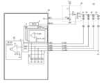
- FIG. 2 is a diagram showing a configuration of a light-emitting system according to the first embodiment of the present disclosure.
- FIG. 3 is a diagram showing a configuration of a light-emitting system according to the second embodiment of the present disclosure.
- FIG. 4 is a diagram showing a configuration of a light-emitting system according to a third embodiment of the present disclosure.
- FIG. 5 is a diagram showing a configuration of a light-emitting system according to a fourth embodiment of the present disclosure.
- FIG. 6 is a diagram showing a configuration of a light-emitting system according to a fifth embodiment of the present disclosure.
- FIG. 1 is a diagram showing a configuration of a light-emitting system according to a comparative example.
- FIG. 2 is a diagram showing a configuration of a light-emitting system according to the first embodiment of the present disclosure.
- FIG. 7 is a diagram showing a configuration of a light-emitting system according to a sixth embodiment of the present disclosure.
- FIG. 8 is a diagram showing a configuration of a light-emitting system according to an eighth embodiment of the present disclosure.
- FIG. 9 is a diagram showing an example of the configuration of a backlight device.
- FIG. 10 is a diagram showing an example of an in-vehicle display.
- Comparative Example Here, a comparative example will be described first for comparison with the embodiment of the present disclosure. By describing the comparative example, the problem will become more clear.
- FIG. 1 is a diagram showing the configuration of a light-emitting system 50 according to a comparative example.
- the light-emitting system 50 shown in FIG. 1 includes an LED driving device (light-emitting element driving device) 20, an output stage 30, and LED arrays 41 to 44.
- the LED driver 20 drives multiple channels (four channels in this embodiment) of LED arrays (light-emitting element units) 41 to 44.
- the LED driver 20 is a semiconductor device that integrates a minimum voltage selection unit 1, a DC/DC control unit 2, a constant current driver 3, an output discharge unit 4, and an output short circuit protection circuit 5 (SCP (short circuit protection)).
- SCP short circuit protection
- the LED driver 20 also has an OUTL terminal, a VDISC terminal, and LED1 to LED4 terminals as external terminals for establishing electrical connection with the outside. Note that for convenience, only a portion of the configuration of the LED driver 20 shown in FIG. 1 is shown, and in reality, the device has other external terminals such as a VCC terminal, and is also provided with an internal voltage generator (VREG) and various protection circuits such as UVLO (Under Voltage Lock Out).
- VREG internal voltage generator
- UVLO Under Voltage Lock Out
- an output stage 30 is arranged to generate an output voltage Vout from an input voltage Vin by DC/DC conversion and supply it to the anodes (positive poles) of the LED arrays 41 to 44.
- the output stage 30 has a switching element N1, a diode D1, an inductor L1, and an output capacitor Co.
- the output stage 30 is controlled by the LED driver 20 as the switching element N1 is driven and controlled by the LED driver 20.
- the output stage 30 and the LED driver 20 form a DC/DC converter.
- a step-up DC/DC converter is particularly configured as the DC/DC converter.
- the application terminal of the input voltage Vin is connected to one terminal of the inductor L1.
- the other terminal of the inductor L1 is connected to the anode of the diode D1 and the drain of a switching element N1 composed of an n-channel metal-oxide-semiconductor field-effect transistor (MOSFET).
- MOSFET metal-oxide-semiconductor field-effect transistor
- the source of the switching element N1 is connected to the ground terminal.
- the gate of the switching element N1 is connected to the OUTL terminal.
- the cathode of the diode D1 is connected to one terminal of the output capacitor Co.
- the other terminal of the output capacitor Co is connected to the ground terminal.
- An output voltage Vout is generated at one terminal of the output capacitor Co.
- the switching element N1 may be included in the LED driving device 20.
- the anodes of the LED arrays 41 to 44 are connected to one end of the output capacitor Co, which generates the output voltage Vout.
- the LED arrays 41 to 44 are each composed of multiple LEDs connected in series.
- the cathodes of the LED arrays 41 to 44 are connected to the LED1 terminal to the LED4 terminal, respectively.
- the LED arrays 41 to 44 are not limited to being connected in series, and may be composed of LEDs connected in series and parallel, or may be composed of only one LED.
- the number of drivable LED arrays (number of channels) is also not limited to four, and may be, for example, six.
- LED terminal voltages Vled1 to Vled4 are applied to the LED1 to LED4 terminals as the cathode voltages of the LED arrays 41 to 44, respectively.
- Minimum voltage selection unit 1 selects the lowest voltage among the LED terminal voltages Vled1 to Vled4.
- the DC/DC control unit 2 has an error amplifier 21.
- the output terminal of the minimum voltage selection unit 1 is connected to the non-inverting input terminal (+) of the error amplifier 21.
- the application terminal of the reference voltage Vref is connected to the inverting input terminal (-) of the error amplifier 21.
- the DC/DC control unit 2 has, for example, a slope generation unit, a PWM comparator, a driver, etc. (not shown) other than the error amplifier 21, and generates a gate signal GS by PWM control based on the error signal between the output of the minimum voltage selection unit 1 and the reference voltage Vref output from the error amplifier 21.
- the generated gate signal GS is applied to the gate of the switching element N1 via the OUTL terminal, thereby controlling the on/off of the switching element N1.
- the output voltage Vout is controlled so that the minimum voltage among the LED terminal voltages Vled1 to Vled4 matches the reference voltage Vref.
- the constant current driver 3 has four channels of constant current circuits 31 arranged between each of the LED1 to LED4 terminals and the ground terminal.
- the constant current value of the current flowing through the constant current circuit 31 can be set by an LED current setting unit (not shown).
- the VDISC terminal is connected to the output discharge unit 4.
- the VDISC terminal is connected to one end of the output capacitor Co where the output voltage Vout is generated. If the output capacitor Co still has charge when started up, the LED may flicker. For this reason, it is desirable for no charge to remain in the output capacitor Co at startup. Therefore, the output discharge unit 4 discharges the residual charge in the output capacitor Co. This discharge is performed when the DC/DC converter is off (when the signal applied to the enable terminal, not shown, falls, or during protection).
- the output short circuit protection circuit (SCP) 5 which is provided as one of the protection functions, has ground fault detection comparators 5A to 5D provided corresponding to each channel of the LED arrays 41 to 44.
- the ground fault detection comparators 5A to 5D have a non-inverting input terminal to which each of the LED terminal voltages Vled1 to Vled4 is applied, and an inverting input terminal to which a reference voltage Vref_sht for ground fault detection is applied.
- the output short circuit protection circuit 5 starts counter operation, and after about 13 ms, for example, the output is latched and all circuits other than the internal voltage generation unit (not shown) are shut down.
- the LED terminal voltage Vled4 will be the lowest compared to the other LED terminal voltages, and the DC/DC converter will perform a boost operation. However, because the LED terminal voltage Vled4 does not rise, the output short-circuit protection circuit 5 stops the operation of the DC/DC converter, and no current flows through the LED arrays 41 to 44. As a result, the LED arrays 41 to 44 are turned off.
- the LED terminal voltage of the channel where the ground fault occurred may not be low enough to be detected by the ground fault detection comparators 5A to 5D.
- ground fault protection is not activated, the DC/DC converter continues to operate, and a larger current than normal flows through the LED array of the channel where the ground fault occurred due to the current path from the cathode to the ground end formed by the ground fault.
- the display device may shine brighter than the set brightness, which may cause problems such as blocking the driver's view.
- excessive current flowing through the LED increases the load on the components in the DC/DC converter, requiring the components to have excess resistance.
- the inventors of the present application have conducted extensive research into a technology that can more reliably detect abnormal light emission from the LED arrays 41-44 (light-emitting element portions), as described below.
- a light-emitting system 501 The configuration of a light-emitting system 501 according to the first embodiment of the present disclosure is shown in Fig. 2.
- the configuration shown in Fig. 2 differs from the comparative example (Fig. 1) in that a current detection resistor R1 is provided outside the LED driving device 201, and further in the configuration of the LED driving device 201 and an MCU (microcomputer) 25. That is, the light-emitting system 501 has a current detection resistor R1 and an MCU 25.
- the first end of the current detection resistor R1 is connected to the application terminal of the output voltage Vout.
- the second end of the current detection resistor R1 is connected to the anodes of the LED arrays 41 to 44. In other words, the current detection resistor R1 is provided after the output stage 30.
- the LED driver 201 has an overcurrent detection unit 6 and an OCD terminal (overcurrent detection terminal) as an external terminal for connecting the current detection resistor R1.
- the overcurrent detection unit 6 has an amplifier 61 and a comparator 62.
- the inverting input terminal of the amplifier 61 is connected to the first terminal of the current detection resistor R1 via the VDISC terminal.
- the non-inverting input terminal of the amplifier 61 is connected to the second terminal of the current detection resistor R1 via the OCD terminal.
- the inverting input terminal of the comparator 62 is connected to the output terminal of the amplifier 61.
- the non-inverting input terminal of the comparator 62 is connected to the application terminal of the reference voltage Va for overcurrent detection.
- the total current Ia which is the sum of the currents flowing through each channel of the LED arrays 41 to 44, is converted to a current/voltage by the current detection resistor R1.
- the converted voltage appears across the current detection resistor R1 and is amplified by an amplifier 61 at a predetermined gain.
- the amplified voltage is compared with a reference voltage Va by the comparator 62, and the comparison result is output as a flag signal Flg.
- the comparator 62 can detect the overcurrent.
- the overcurrent detection unit 6 can detect an overcurrent in the current flowing through the LED arrays 41 to 44 (light-emitting element unit).
- the LED driver 201 has an FG terminal (flag terminal) and an EN terminal (enable terminal) as external terminals.
- the MCU 25 is externally connected to the FG terminal and the EN terminal.
- the flag signal Flg output from the comparator 62 is input to the MCU 25 via the FG terminal.
- the MCU 25 can output the enable signal Eb via the EN terminal to an internal voltage generator 7 provided in the LED driver 201.
- the internal voltage generator 7 generates an internal power supply voltage Vreg based on a power supply voltage applied to a VCC terminal (not shown) provided in the LED driver 201.
- the internal power supply voltage Vreg is generated when the enable signal Eb is in an enabled state, and is used as a power supply voltage for the internal circuit of the LED driver 201.
- the MCU 25 disables the enable signal Eb. This stops the operation of the internal voltage generation unit 7, and the internal power supply voltage Vreg drops.
- the UVLO unit 8 provided in the LED drive device 201 detects the drop in the internal power supply voltage Vreg and commands the DC/DC control unit 2 to stop the operation of the DC/DC converter. This stops the switching of the switching element N1, stops current flowing to the LED arrays 41 to 44, and releases the abnormal light emission state.
- Second Embodiment 3 is a diagram showing the configuration of a light-emitting system 502 according to a second embodiment of the present disclosure.
- the difference in configuration from the first embodiment (FIG. 2) of the configuration shown in FIG. 3 is the configurations of the LED driver 202 and the MCU 25.
- the LED driver 202 has an LED current setting unit 9 and a communication unit 10. Note that the LED current setting unit 9 is also provided in the first embodiment.
- the communication unit 10 is configured to communicate with the MCU 25, for example, by SPI (Serial Peripheral Interface).
- the communication unit 10 has a register 10A. Various types of information are stored in the register 10A.
- the LED driver 202 has an ADIM terminal (dimming terminal) as an external terminal.
- the MCU 25 can dim the LED arrays 41 to 44 by outputting a dimming signal Dm to the LED current setting unit 9 via the ADIM terminal. This type of dimming is called DC dimming.
- the LED current setting unit 9 has an error amplifier 91 and an output transistor 92.
- the non-inverting input terminal of the error amplifier 91 is connected to the application terminal of the reference voltage Vref_led for setting the LED current.
- the output terminal of the error amplifier 91 is connected to the gate of the output transistor 92 composed of an n-channel MOSFET.
- the source of the output transistor 92 is connected to the inverting input terminal of the error amplifier 91.
- the LED driver 202 has an ISET terminal (current setting terminal) as an external terminal.
- the first terminal of the setting resistor Reset is externally connected to the ISET terminal.
- the ISET terminal is connected to the source of the output transistor 92.
- the voltage at the ISET terminal is controlled to match the reference voltage Vref_led, and a current flows through the ISET terminal at a current value determined by the voltage at the ISET terminal and the setting resistor Reset.
- a current proportional to the current flowing through the ISET terminal flows through each constant current circuit 31.
- the reference voltage Vref_led is variable according to the dimming signal Dm, and the LED current can be set by the dimming signal Dm.
- the operation of the DC/DC converter may be stopped by disabling the enable signal Eb, as in the first embodiment.
- the communication unit 10 may not be provided, and when the MCU 25 receives a flag signal Flg indicating an abnormality from the FG terminal, as in the first embodiment, the dimming signal Dm may be used to dim the LEDs to reduce their brightness.
- Third Embodiment 4 is a diagram showing the configuration of a light-emitting system 503 according to a third embodiment of the present disclosure.
- the difference in configuration from the second embodiment (FIG. 3) of the configuration shown in FIG. 4 is the configuration of the LED driving device 203.
- the LED driver 203 has a flag output unit 11.
- the flag output unit 11 In addition to the output Cp1 of the comparator 62 in the overcurrent detection unit 6, the flag output unit 11 also receives outputs from various protection circuits 12 (SCP, TSD (thermal shutdown), UVLO, etc.) not shown.
- the flag output unit 11 outputs a flag signal Flg from the FLG terminal to the MCU 25 based on Cp1 and the outputs from the various protection circuits 12. Specifically, if any one of the outputs including Cp1 indicates an abnormality, the flag signal Flg reaches a level indicating an abnormality.
- the MCU 25 When the MCU 25 receives a flag signal Flg with a level indicating an abnormality, it communicates with the communication unit 10 to read the register 10A in order to determine the specific type of abnormality.
- the register 10A stores information indicating which abnormality has been detected by the overcurrent detection unit 6 and the various protection circuits 12.
- the MCU 25 When the MCU 25 reads the register 10A and determines that an overcurrent abnormality has been detected by the overcurrent detection unit 6, the MCU 25 performs dimming to reduce the brightness of the LED using the dimming signal Dm, as in the second embodiment.
- the MCU 25 may stop the operation of the DC/DC converter using the enable signal Eb, for example, when an overcurrent abnormality has been detected by the overcurrent detection unit 6 and a ground fault has been detected at the cathode of the LED by the output short circuit protection circuit (SCP).
- SCP output short circuit protection circuit
- FIG. 5 is a diagram showing the configuration of a light-emitting system 504 according to a fourth embodiment of the present disclosure.
- the difference in configuration from the first embodiment (Fig. 2) of the configuration shown in Fig. 5 is that current detection resistors Ra to Rd are provided. That is, the light-emitting system 504 has current detection resistors Ra to Rd.
- Current detection resistors Ra to Rd are provided corresponding to each channel of the LED arrays 41 to 44. Specifically, the first terminals of the current detection resistors Ra to Rd are commonly connected to the application terminal of the output voltage Vout. The second terminals of the current detection resistors Ra to Rd are connected to the anodes of the LED arrays 41 to 44, respectively.
- the LED driver 204 has overcurrent detection units 6A to 6D and terminals OCD1 to OCD4.
- the overcurrent detection units 6A to 6D are provided corresponding to each channel of the LED arrays 41 to 44.
- Each of the overcurrent detection units 6A to 6D has an amplifier 61 and a comparator 62. More specifically, a first end of the current detection resistor Ra is connected to the inverting input end of the amplifier 61 of the overcurrent detection unit 6A, and a second end of the current detection resistor Ra is connected to the non-inverting input end of the amplifier 61 of the overcurrent detection unit 6A via the OCD1 terminal. Similarly, both ends of resistors Rb, Rc, and Rd are connected to the input ends of the amplifier 61 of the overcurrent detection units 6B to 6D.
- the LED driver 204 has terminals FG1 to FG4 corresponding to the overcurrent detectors 6A to 6D.
- the flag signals Flg1 to Flg4 output from the comparators 62 of the overcurrent detectors 6A to 6D are sent to the MCU 25 via the terminals FG1 to FG4, respectively.
- the overcurrent detection units 6A to 6D can detect overcurrent for each channel of the LED arrays 41 to 44. Therefore, the MCU 25 can determine in which channel an overcurrent abnormality is occurring, based on the flag signals Flg1 to Flg4.
- the LED driver 204 has LED current setting units 9A to 9D.
- the LED current setting units 9A to 9D are provided corresponding to each channel of the LED arrays 41 to 44.
- Each of the LED current setting units 9A to 9D has an error amplifier 91 and an output transistor 92.
- the setting resistor Reset may be shared by the LED current setting units 9A to 9D, or may be provided for each of the LED current setting units 9A to 9D.
- the LED driver 204 has ADIM1 terminals to ADIM4 terminals corresponding to the LED current setting units 9A to 9D.
- the MCU 25 outputs dimming signals Dm1 to Dm4 to the LED current setting units 9A to 9D via the ADIM1 to ADIM4 terminals, respectively.
- the dimming signal Dm1 varies the reference voltage Vref_led1 in the LED current setting unit 9A, and the dimming signal Dm1 enables dimming of the LED array 41 (first channel).
- the dimming signals Dm2 to Dm4 vary the reference voltages Vref_led2 to Vref_led4 in the LED current setting units 9B to 9D, respectively, and the dimming signals Dm2 to Dm4 enable dimming of the LED arrays 42 to 44 (second to fourth channels).
- the MCU 25 determines which channel an overcurrent abnormality is occurring in based on the flag signals Flg1 to Flg4, and performs dimming to reduce the LED brightness using the dimming signals Dm1 to Dm4 corresponding to the determined channel. For example, if an overcurrent abnormality is occurring in the LED array 44 of the fourth channel, the overcurrent abnormality is detected by the flag signal Flg4, and the reference voltage Vref_led4 in the LED current setting unit 9D is changed by the dimming signal Dm4 so that it is lower than normal. This suppresses abnormal light emission in the fourth channel.
- overcurrent abnormalities can be detected for each channel and only the abnormal channel can be dimmed, so protection can be achieved without reducing the brightness of the entire LED array 41 to 44 as much as possible.
- the FG1 to FG4 terminals may not be provided, but a communication unit 10 may be provided, the output states of the overcurrent detection units 6A to 6D may be stored in a register 10A of the communication unit 10, and the MCU 25 may read the register 10A via communication. This also allows the MCU 25 to determine in which channel an overcurrent abnormality is occurring.
- Fifth Embodiment 6 is a diagram showing a configuration of a light-emitting system 505 according to a fifth embodiment of the present disclosure.
- a current detection resistor Ra is provided corresponding to the pair of LED arrays 41 and 42 (first and second channels), and a resistor Rb is provided corresponding to the pair of LED arrays 43 and 44 (third and fourth channels). More specifically, the first terminals of the current detection resistors Ra and Rb are commonly connected to the application terminal of the output voltage Vout, the second terminals of the current detection resistor Ra are connected to the anodes of the LED arrays 41 and 42, and the second terminals of the resistor Rb are connected to the anodes of the LED arrays 43 and 44.
- LED driving device 205 of this embodiment overcurrent detection units 6A, 6B and OCD1, OCD2 terminals are provided corresponding to the current detection resistors Ra, Rb.
- FG1, FG2 terminals are provided as flag terminals
- ADIM1, ADIM2 terminals are provided as dimming terminals
- LED current setting units 9A, 9B are provided.
- LED current setting units 9A, 9B correspond to the set of LED arrays 41, 42 and the set of LED arrays 43, 44, respectively.
- This configuration makes it possible to detect overcurrent abnormalities and adjust the brightness for each pair of LED arrays 41 and 42 and for each pair of LED arrays 43 and 44. This makes it possible to reduce the number of external terminals in the LED driving device while achieving the same effect as the fourth embodiment.
- Sixth Embodiment 7 is a diagram showing a configuration of a light-emitting system 506 according to a sixth embodiment of the present disclosure.
- an MCU as in the first to fifth embodiments is not used.
- the LED driving device 206 of this embodiment has a dimming control unit 13.
- the dimming control unit 13 variably controls the reference voltage Vref_led in the LED current setting unit 9.
- the dimming control unit 13 changes Vref_led in the LED current setting unit 9 to be lower than normal. This reduces the currents flowing through the LED arrays 41 to 44, providing protection. According to this embodiment, protection can be achieved by feedback to the LED current setting unit 9 within the LED driver 206, without using an MCU.
- the dimming control unit 13 may control the LED current setting unit 9 corresponding to the channel in which an overcurrent abnormality is detected. This makes it possible to obtain the same effect as the fourth or fifth embodiment without using an MCU.
- the reference voltage Va for detecting an overcurrent may be variable.
- the reference voltage Va may be variable based on a setting resistor Reset externally connected to an ISET terminal (current setting terminal).
- the overcurrent threshold value can be set according to the LED current setting.
- FIG. 8 is a diagram showing a configuration of a light-emitting system 507 according to an eighth embodiment of the present disclosure.
- a p-channel MOSFET 35 is provided in addition to a current detection resistor R1.
- a first end of the current detection resistor R1 is connected to the application end of the output voltage Vout.
- a second end of the current detection resistor R1 is connected to the source of the p-channel MOSFET 35 at node N1.
- the drain of the p-channel MOSFET 35 is connected to each anode of the LED arrays 41 to 44.
- the LED driving device 207 of this embodiment has an overcurrent detection unit 14.
- the LED driving device 207 also has a PGT terminal (gate connection terminal) as an external terminal.
- the overcurrent detection unit 14 has a current limiting unit 141 and a comparator 142.
- the current limiting unit 141 has an amplifier 141A.
- the inverting input terminal of the amplifier 141A is connected to the node N1 via the OCD terminal.
- a voltage that is lower than the output voltage Vout by the reference voltage Vb1 is applied to the non-inverting input terminal of the amplifier 141A.
- the output terminal of the amplifier 141A is connected to the gate (control terminal) of the p-channel MOSFET 35 via the PGT terminal.
- the amplifier 141A controls the gate voltage of the p-channel MOSFET 35 to be higher. This increases the impedance between the drain and source of the p-channel MOSFET 35. This reduces the total current Ia, and the current flowing through the LED arrays 41 to 44 is suppressed.
- the reference voltage Vb1 in the current limiting unit 141 is set to a voltage value corresponding to a current setting value greater than the maximum value of the total current Ia due to current value variation in the constant current driver 3.
- the non-inverting input terminal of the comparator 142 is connected to the PGT terminal.
- the inverting input terminal of the comparator 142 is connected to the application terminal of the reference voltage Vb2. This causes the comparator 142 to output the comparison result between the gate voltage of the p-channel MOSFET 35 and the reference voltage Vb2.
- a backlight device will be described as an example of an application of the LED driving device according to the embodiment described above.
- a configuration example of a backlight device to which the LED driving device can be applied is shown in Fig. 9. Note that the configuration shown in Fig. 9 is a so-called edge light type, but is not limited to this and may be a direct type configuration.
- the backlight device 70 shown in FIG. 9 is an illumination device that illuminates the liquid crystal panel 81 from the back.
- the backlight device 70 includes an LED light source device 71, a light guide plate 72, a reflector plate 73, and optical sheets 74.
- the LED light source device 71 includes an LED and a substrate on which the LED is mounted. Light emitted from the LED light source device 71 enters the interior from the side of the light guide plate 72.
- the light guide plate 72 which is made of an acrylic plate, for example, totally reflects the light that enters the interior and guides it throughout the interior, and emits it as planar light from the side on which the optical sheets 74 are arranged.
- the reflector plate 73 reflects the light leaking from the light guide plate 72 back into the light guide plate 72.
- the optical sheets 74 are made of a diffusion sheet, a lens sheet, etc., and are intended to uniformize and improve the brightness of the light illuminating the liquid crystal panel 81.
- the light emitting system of the various embodiments described above can be used as the LED light source device 71.
- a backlight device to which the LED driving device according to the embodiment described above is applied is particularly suitable for mounting on an in-vehicle display.
- the in-vehicle display is mounted on the dashboard in front of the driver's seat of the vehicle, for example, as in the in-vehicle display 85 shown in FIG. 10.
- the in-vehicle display 85 can display various images, such as car navigation information, captured images of the rear of the vehicle, a speedometer, a fuel gauge, a fuel consumption meter, and a shift position, and can convey various information to the user.
- Such an in-vehicle display is also called a cluster panel or a center information display (CID).
- the in-vehicle display may be a rear entertainment device disposed, for example, behind the driver's seat or passenger seat.
- the light-emitting element driving device (201) is configured to be connectable to at least one current detection resistor (R1) provided between the application terminal of a power supply voltage (Vout) for driving at least one channel of a light-emitting element unit (41 to 44) and the positive electrode of the light-emitting element unit, and is configured to detect an overcurrent of a current flowing in the light-emitting element unit (first configuration).
- R1 current detection resistor
- the overcurrent detection unit (6) may be configured to have an amplifier (61) having an input terminal configured to be connected to the current detection resistor (R1), and a first comparator (62) configured to compare the output of the amplifier with a first reference voltage (Va) (second configuration).
- a constant current driver (3) configured to be connectable to a negative electrode of the light-emitting element unit; a current setting terminal (ISET terminal) which is an external terminal connectable to a setting resistor (Reset); a current setting unit (9) configured to set a current value of the constant current driver based on the setting resistor; Equipped with The first reference voltage (Va) may be variably set based on the setting resistor (third configuration).
- an external terminal may be provided for outputting the detection result of the overcurrent detection unit (6) to the outside (fourth configuration).
- the external terminal may be configured to be connectable to an external MCU (25) (fifth configuration).
- the sixth configuration may include a flag output unit (11) configured to generate a flag signal (Flg) based on the detection result by the protection circuit in addition to the detection result and output the flag signal via the external terminal.
- a configuration may be provided that includes a register (10A) capable of storing the detection result of the overcurrent detection unit as information, and a communication unit (10) configured to be capable of communicating with an external MCU (25) (seventh configuration).
- a constant current driver (3) configured to be connectable to a negative electrode of the light-emitting element unit;
- a current setting unit (9) configured to set a current value of the constant current driver;
- the eighth configuration may further include a dimming control unit (13) configured to cause the current setting unit to set the current value lower than normal when an overcurrent abnormality is detected by the overcurrent detection unit (6).
- the current detection resistors (Ra to Rd) may be provided for each of the multiple channels, and the overcurrent detection units (6A to 6D) may be provided for each of the multiple current detection resistors (ninth configuration, FIG. 5).
- the current detection resistors (Ra, Rb) may be provided for each of a plurality of groups consisting of a plurality of the channels, and the overcurrent detection units (6A, 6B) may be provided for each of the plurality of current detection resistors (tenth configuration, FIG. 6).
- a light-emitting system (501) includes a light-emitting element driving device (201) having any one of the first to tenth configurations described above, the current detection resistor (R1), an MCU (25), and a DC/DC converter configured to generate the power supply voltage (Vout), and when an overcurrent abnormality is detected by the overcurrent detection unit (6), the MCU is configured to instruct the light-emitting element driving device to stop the operation of the DC/DC converter (eleventh configuration).
- a light-emitting system (502) includes a light-emitting element driving device (202) having any one of the first to tenth configurations, the current detection resistor (R1), and an MCU (25),
- the light-emitting element driving device (202) includes a constant current driver (3) configured to be connectable to a negative electrode of the light-emitting element unit, and a current setting unit (9) configured to set a current value of the constant current driver,
- the MCU is configured to send a dimming signal (Dm) to the light-emitting element driving device so as to cause the current setting unit to set the current value lower than normal (12th configuration).
- a light-emitting system (507) includes a light-emitting element driving device (207) having any one of the first to tenth configurations described above, the current detection resistor (R1), and a transistor (35) connected between the current detection resistor and the positive electrode of the light-emitting element portion, and the overcurrent detection unit (14) has a current limiting unit (141) configured to limit the current flowing through the current detection resistor by controlling the control terminal of the transistor, and is configured to detect the overcurrent based on the voltage of the control terminal (13th configuration).
- the current limiting unit (141) may be configured to have an amplifier (141A) including a first input terminal configured to be connectable to a node (N1) to which the current detection resistor (R1) and the transistor (35) are connected, a second input terminal configured to be connected to an application terminal of a voltage lower than a predetermined voltage (Vout) by a second reference voltage (Vb1), and an output terminal configured to be connectable to the control terminal (14th configuration).
- an amplifier (141A) including a first input terminal configured to be connectable to a node (N1) to which the current detection resistor (R1) and the transistor (35) are connected, a second input terminal configured to be connected to an application terminal of a voltage lower than a predetermined voltage (Vout) by a second reference voltage (Vb1), and an output terminal configured to be connectable to the control terminal (14th configuration).
- the overcurrent detection unit (14) may be configured to have a third comparator (142) including a first input terminal configured to be connected to the control terminal and a second input terminal configured to be connected to an application terminal of a third reference voltage (Vb2) (15th configuration).
- a third comparator 142
- Vb2 third reference voltage
- the transistor (35) may be a p-channel MOSFET (configuration 16).
- a lighting device (70) includes a light-emitting element driving device having any one of the first to tenth configurations described above, or a light-emitting system having any one of the eleventh to sixteenth configurations described above (seventeenth configuration).
- an in-vehicle display device (85) includes an illumination device having the 17th configuration described above (18th configuration).
- This disclosure can be used, for example, as a driving means for in-vehicle LEDs.
Landscapes
- Circuit Arrangement For Electric Light Sources In General (AREA)
Priority Applications (1)
| Application Number | Priority Date | Filing Date | Title |
|---|---|---|---|
| JP2024555739A JPWO2024075591A1 (https=) | 2022-10-06 | 2023-09-26 |
Applications Claiming Priority (2)
| Application Number | Priority Date | Filing Date | Title |
|---|---|---|---|
| JP2022-161712 | 2022-10-06 | ||
| JP2022161712 | 2022-10-06 |
Publications (1)
| Publication Number | Publication Date |
|---|---|
| WO2024075591A1 true WO2024075591A1 (ja) | 2024-04-11 |
Family
ID=90608263
Family Applications (1)
| Application Number | Title | Priority Date | Filing Date |
|---|---|---|---|
| PCT/JP2023/034912 Ceased WO2024075591A1 (ja) | 2022-10-06 | 2023-09-26 | 発光素子駆動装置、および発光システム |
Country Status (2)
| Country | Link |
|---|---|
| JP (1) | JPWO2024075591A1 (https=) |
| WO (1) | WO2024075591A1 (https=) |
Citations (6)
| Publication number | Priority date | Publication date | Assignee | Title |
|---|---|---|---|---|
| JP2014003770A (ja) * | 2012-06-15 | 2014-01-09 | Rohm Co Ltd | 電源装置、並びに、これを用いた車載機器及び車両 |
| JP2016122643A (ja) * | 2014-09-16 | 2016-07-07 | 株式会社小糸製作所 | 点灯回路およびそれを用いた車両用灯具 |
| JP2017195150A (ja) * | 2016-04-22 | 2017-10-26 | ローム株式会社 | 発光素子駆動用半導体集積回路、発光素子駆動装置、発光装置、車両 |
| JP2018014310A (ja) * | 2016-07-12 | 2018-01-25 | パナソニックIpマネジメント株式会社 | 点灯装置及びそれを備える照明器具 |
| JP2018019498A (ja) * | 2016-07-27 | 2018-02-01 | ローム株式会社 | 半導体装置 |
| WO2021106360A1 (ja) * | 2019-11-27 | 2021-06-03 | ローム株式会社 | Led駆動装置、照明装置、および車載用表示装置 |
-
2023
- 2023-09-26 JP JP2024555739A patent/JPWO2024075591A1/ja active Pending
- 2023-09-26 WO PCT/JP2023/034912 patent/WO2024075591A1/ja not_active Ceased
Patent Citations (6)
| Publication number | Priority date | Publication date | Assignee | Title |
|---|---|---|---|---|
| JP2014003770A (ja) * | 2012-06-15 | 2014-01-09 | Rohm Co Ltd | 電源装置、並びに、これを用いた車載機器及び車両 |
| JP2016122643A (ja) * | 2014-09-16 | 2016-07-07 | 株式会社小糸製作所 | 点灯回路およびそれを用いた車両用灯具 |
| JP2017195150A (ja) * | 2016-04-22 | 2017-10-26 | ローム株式会社 | 発光素子駆動用半導体集積回路、発光素子駆動装置、発光装置、車両 |
| JP2018014310A (ja) * | 2016-07-12 | 2018-01-25 | パナソニックIpマネジメント株式会社 | 点灯装置及びそれを備える照明器具 |
| JP2018019498A (ja) * | 2016-07-27 | 2018-02-01 | ローム株式会社 | 半導体装置 |
| WO2021106360A1 (ja) * | 2019-11-27 | 2021-06-03 | ローム株式会社 | Led駆動装置、照明装置、および車載用表示装置 |
Also Published As
| Publication number | Publication date |
|---|---|
| JPWO2024075591A1 (https=) | 2024-04-11 |
Similar Documents
| Publication | Publication Date | Title |
|---|---|---|
| JP5341067B2 (ja) | Led故障検出回路 | |
| US8283870B2 (en) | Bypass protection circuit and light emitting diode driving device using the same | |
| US8878445B2 (en) | Light-emitting element driving device | |
| US8581512B2 (en) | Light source module, lighting apparatus, and illumination device using the same | |
| KR101712676B1 (ko) | Pwm 제어 회로 및 이를 이용한 led 구동회로 | |
| US20110080117A1 (en) | Distributed architecture voltage controlled backlight driver | |
| JP7518856B2 (ja) | Led駆動装置、照明装置、および車載用表示装置 | |
| US9125268B2 (en) | Power supply for LED illumination | |
| KR20170045218A (ko) | Led 주행등 제어 및 상태를 위한 장치 및 방법 | |
| JP2008258428A (ja) | 照明用白色led駆動回路並びにこれを備えた照明装置及び電子機器 | |
| JP6783790B2 (ja) | 点灯回路、車両用灯具 | |
| US8786129B2 (en) | Control device for lighting LED and detecting breakage thereof | |
| US11906123B2 (en) | Light source module | |
| CN103260323B (zh) | 电源控制电路、短路侦测电路以及控制方法 | |
| US12446132B2 (en) | LED driving device, LED light source device, and vehicle onboard display device | |
| JP2018019497A (ja) | 半導体装置 | |
| CN111986625A (zh) | 背光驱动电路及显示装置 | |
| EP1774834A1 (en) | Power supply system and method for automative led lighting systems | |
| JP2009016459A (ja) | 駆動装置及び照明装置 | |
| JP5203320B2 (ja) | 発光素子駆動装置およびそれを備えた面状照明装置または表示装置 | |
| JP2023101804A (ja) | ランプ制御装置 | |
| WO2024075591A1 (ja) | 発光素子駆動装置、および発光システム | |
| CN115299181B (zh) | 光源模块以及点亮电路 | |
| CN214757027U (zh) | 背光电路及显示面板 | |
| CN220254717U (zh) | 可调光的led驱动电路 |
Legal Events
| Date | Code | Title | Description |
|---|---|---|---|
| 121 | Ep: the epo has been informed by wipo that ep was designated in this application |
Ref document number: 23874719 Country of ref document: EP Kind code of ref document: A1 |
|
| WWE | Wipo information: entry into national phase |
Ref document number: 2024555739 Country of ref document: JP |
|
| NENP | Non-entry into the national phase |
Ref country code: DE |
|
| 122 | Ep: pct application non-entry in european phase |
Ref document number: 23874719 Country of ref document: EP Kind code of ref document: A1 |