WO2024062829A1 - 半導体装置及び高周波電力増幅器 - Google Patents
半導体装置及び高周波電力増幅器 Download PDFInfo
- Publication number
- WO2024062829A1 WO2024062829A1 PCT/JP2023/030322 JP2023030322W WO2024062829A1 WO 2024062829 A1 WO2024062829 A1 WO 2024062829A1 JP 2023030322 W JP2023030322 W JP 2023030322W WO 2024062829 A1 WO2024062829 A1 WO 2024062829A1
- Authority
- WO
- WIPO (PCT)
- Prior art keywords
- base
- emitter
- layer
- collector
- electrode
- Prior art date
- Legal status (The legal status is an assumption and is not a legal conclusion. Google has not performed a legal analysis and makes no representation as to the accuracy of the status listed.)
- Ceased
Links
Images











Classifications
-
- H—ELECTRICITY
- H10—SEMICONDUCTOR DEVICES; ELECTRIC SOLID-STATE DEVICES NOT OTHERWISE PROVIDED FOR
- H10D—INORGANIC ELECTRIC SEMICONDUCTOR DEVICES
- H10D10/00—Bipolar junction transistors [BJT]
- H10D10/80—Heterojunction BJTs
- H10D10/821—Vertical heterojunction BJTs
- H10D10/841—Vertical heterojunction BJTs having a two-dimensional base, e.g. modulation-doped base, inversion layer base or delta-doped base
-
- H—ELECTRICITY
- H03—ELECTRONIC CIRCUITRY
- H03F—AMPLIFIERS
- H03F3/00—Amplifiers with only discharge tubes or only semiconductor devices as amplifying elements
- H03F3/189—High-frequency amplifiers, e.g. radio frequency amplifiers
- H03F3/19—High-frequency amplifiers, e.g. radio frequency amplifiers with semiconductor devices only
- H03F3/195—High-frequency amplifiers, e.g. radio frequency amplifiers with semiconductor devices only in integrated circuits
-
- H—ELECTRICITY
- H03—ELECTRONIC CIRCUITRY
- H03F—AMPLIFIERS
- H03F3/00—Amplifiers with only discharge tubes or only semiconductor devices as amplifying elements
- H03F3/20—Power amplifiers, e.g. Class B amplifiers, Class C amplifiers
- H03F3/21—Power amplifiers, e.g. Class B amplifiers, Class C amplifiers with semiconductor devices only
- H03F3/213—Power amplifiers, e.g. Class B amplifiers, Class C amplifiers with semiconductor devices only in integrated circuits
-
- H—ELECTRICITY
- H03—ELECTRONIC CIRCUITRY
- H03F—AMPLIFIERS
- H03F3/00—Amplifiers with only discharge tubes or only semiconductor devices as amplifying elements
- H03F3/20—Power amplifiers, e.g. Class B amplifiers, Class C amplifiers
- H03F3/24—Power amplifiers, e.g. Class B amplifiers, Class C amplifiers of transmitter output stages
- H03F3/245—Power amplifiers, e.g. Class B amplifiers, Class C amplifiers of transmitter output stages with semiconductor devices only
-
- H—ELECTRICITY
- H10—SEMICONDUCTOR DEVICES; ELECTRIC SOLID-STATE DEVICES NOT OTHERWISE PROVIDED FOR
- H10D—INORGANIC ELECTRIC SEMICONDUCTOR DEVICES
- H10D10/00—Bipolar junction transistors [BJT]
- H10D10/01—Manufacture or treatment
- H10D10/021—Manufacture or treatment of heterojunction BJTs [HBT]
-
- H—ELECTRICITY
- H10—SEMICONDUCTOR DEVICES; ELECTRIC SOLID-STATE DEVICES NOT OTHERWISE PROVIDED FOR
- H10D—INORGANIC ELECTRIC SEMICONDUCTOR DEVICES
- H10D10/00—Bipolar junction transistors [BJT]
- H10D10/01—Manufacture or treatment
- H10D10/051—Manufacture or treatment of vertical BJTs
- H10D10/056—Manufacture or treatment of vertical BJTs of vertical BJTs having the main current going through the whole substrate, e.g. power BJTs
- H10D10/058—Manufacture or treatment of vertical BJTs of vertical BJTs having the main current going through the whole substrate, e.g. power BJTs having multi-emitter structures, e.g. interdigitated, multi-cellular or distributed emitters
-
- H—ELECTRICITY
- H10—SEMICONDUCTOR DEVICES; ELECTRIC SOLID-STATE DEVICES NOT OTHERWISE PROVIDED FOR
- H10D—INORGANIC ELECTRIC SEMICONDUCTOR DEVICES
- H10D10/00—Bipolar junction transistors [BJT]
- H10D10/80—Heterojunction BJTs
- H10D10/821—Vertical heterojunction BJTs
-
- H—ELECTRICITY
- H10—SEMICONDUCTOR DEVICES; ELECTRIC SOLID-STATE DEVICES NOT OTHERWISE PROVIDED FOR
- H10D—INORGANIC ELECTRIC SEMICONDUCTOR DEVICES
- H10D62/00—Semiconductor bodies, or regions thereof, of devices having potential barriers
- H10D62/10—Shapes, relative sizes or dispositions of the regions of the semiconductor bodies; Shapes of the semiconductor bodies
- H10D62/124—Shapes, relative sizes or dispositions of the regions of semiconductor bodies or of junctions between the regions
- H10D62/126—Top-view geometrical layouts of the regions or the junctions
-
- H—ELECTRICITY
- H10—SEMICONDUCTOR DEVICES; ELECTRIC SOLID-STATE DEVICES NOT OTHERWISE PROVIDED FOR
- H10D—INORGANIC ELECTRIC SEMICONDUCTOR DEVICES
- H10D62/00—Semiconductor bodies, or regions thereof, of devices having potential barriers
- H10D62/10—Shapes, relative sizes or dispositions of the regions of the semiconductor bodies; Shapes of the semiconductor bodies
- H10D62/13—Semiconductor regions connected to electrodes carrying current to be rectified, amplified or switched, e.g. source or drain regions
- H10D62/133—Emitter regions of BJTs
- H10D62/136—Emitter regions of BJTs of heterojunction BJTs
-
- H—ELECTRICITY
- H10—SEMICONDUCTOR DEVICES; ELECTRIC SOLID-STATE DEVICES NOT OTHERWISE PROVIDED FOR
- H10D—INORGANIC ELECTRIC SEMICONDUCTOR DEVICES
- H10D62/00—Semiconductor bodies, or regions thereof, of devices having potential barriers
- H10D62/80—Semiconductor bodies, or regions thereof, of devices having potential barriers characterised by the materials
- H10D62/85—Semiconductor bodies, or regions thereof, of devices having potential barriers characterised by the materials being Group III-V materials, e.g. GaAs
- H10D62/852—Semiconductor bodies, or regions thereof, of devices having potential barriers characterised by the materials being Group III-V materials, e.g. GaAs being Group III-V materials comprising three or more elements, e.g. AlGaN or InAsSbP
-
- H—ELECTRICITY
- H10—SEMICONDUCTOR DEVICES; ELECTRIC SOLID-STATE DEVICES NOT OTHERWISE PROVIDED FOR
- H10D—INORGANIC ELECTRIC SEMICONDUCTOR DEVICES
- H10D64/00—Electrodes of devices having potential barriers
- H10D64/20—Electrodes characterised by their shapes, relative sizes or dispositions
- H10D64/23—Electrodes carrying the current to be rectified, amplified, oscillated or switched, e.g. sources, drains, anodes or cathodes
- H10D64/231—Emitter or collector electrodes for bipolar transistors
-
- H—ELECTRICITY
- H10—SEMICONDUCTOR DEVICES; ELECTRIC SOLID-STATE DEVICES NOT OTHERWISE PROVIDED FOR
- H10D—INORGANIC ELECTRIC SEMICONDUCTOR DEVICES
- H10D64/00—Electrodes of devices having potential barriers
- H10D64/20—Electrodes characterised by their shapes, relative sizes or dispositions
- H10D64/27—Electrodes not carrying the current to be rectified, amplified, oscillated or switched, e.g. gates
- H10D64/281—Base electrodes for bipolar transistors
-
- H—ELECTRICITY
- H10—SEMICONDUCTOR DEVICES; ELECTRIC SOLID-STATE DEVICES NOT OTHERWISE PROVIDED FOR
- H10D—INORGANIC ELECTRIC SEMICONDUCTOR DEVICES
- H10D84/00—Integrated devices formed in or on semiconductor substrates that comprise only semiconducting layers, e.g. on Si wafers or on GaAs-on-Si wafers
-
- H—ELECTRICITY
- H10—SEMICONDUCTOR DEVICES; ELECTRIC SOLID-STATE DEVICES NOT OTHERWISE PROVIDED FOR
- H10D—INORGANIC ELECTRIC SEMICONDUCTOR DEVICES
- H10D84/00—Integrated devices formed in or on semiconductor substrates that comprise only semiconducting layers, e.g. on Si wafers or on GaAs-on-Si wafers
- H10D84/01—Manufacture or treatment
- H10D84/0112—Integrating together multiple components covered by H10D8/00, H10D10/00 or H10D18/00, e.g. integrating multiple BJTs
-
- H—ELECTRICITY
- H10—SEMICONDUCTOR DEVICES; ELECTRIC SOLID-STATE DEVICES NOT OTHERWISE PROVIDED FOR
- H10D—INORGANIC ELECTRIC SEMICONDUCTOR DEVICES
- H10D84/00—Integrated devices formed in or on semiconductor substrates that comprise only semiconducting layers, e.g. on Si wafers or on GaAs-on-Si wafers
- H10D84/01—Manufacture or treatment
- H10D84/02—Manufacture or treatment characterised by using material-based technologies
- H10D84/03—Manufacture or treatment characterised by using material-based technologies using Group IV technology, e.g. silicon technology or silicon-carbide [SiC] technology
- H10D84/038—Manufacture or treatment characterised by using material-based technologies using Group IV technology, e.g. silicon technology or silicon-carbide [SiC] technology using silicon technology, e.g. SiGe
-
- H—ELECTRICITY
- H10—SEMICONDUCTOR DEVICES; ELECTRIC SOLID-STATE DEVICES NOT OTHERWISE PROVIDED FOR
- H10D—INORGANIC ELECTRIC SEMICONDUCTOR DEVICES
- H10D84/00—Integrated devices formed in or on semiconductor substrates that comprise only semiconducting layers, e.g. on Si wafers or on GaAs-on-Si wafers
- H10D84/60—Integrated devices formed in or on semiconductor substrates that comprise only semiconducting layers, e.g. on Si wafers or on GaAs-on-Si wafers characterised by the integration of at least one component covered by groups H10D10/00 or H10D18/00, e.g. integration of BJTs
- H10D84/611—Combinations of BJTs and one or more of diodes, resistors or capacitors
- H10D84/613—Combinations of vertical BJTs and one or more of diodes, resistors or capacitors
- H10D84/615—Combinations of vertical BJTs and one or more of resistors or capacitors
-
- H—ELECTRICITY
- H10—SEMICONDUCTOR DEVICES; ELECTRIC SOLID-STATE DEVICES NOT OTHERWISE PROVIDED FOR
- H10W—GENERIC PACKAGES, INTERCONNECTIONS, CONNECTORS OR OTHER CONSTRUCTIONAL DETAILS OF DEVICES COVERED BY CLASS H10
- H10W20/00—Interconnections in chips, wafers or substrates
- H10W20/20—Interconnections within wafers or substrates, e.g. through-silicon vias [TSV]
-
- H—ELECTRICITY
- H03—ELECTRONIC CIRCUITRY
- H03F—AMPLIFIERS
- H03F2200/00—Indexing scheme relating to amplifiers
- H03F2200/318—A matching circuit being used as coupling element between two amplifying stages
-
- H—ELECTRICITY
- H03—ELECTRONIC CIRCUITRY
- H03F—AMPLIFIERS
- H03F2200/00—Indexing scheme relating to amplifiers
- H03F2200/411—Indexing scheme relating to amplifiers the output amplifying stage of an amplifier comprising two power stages
-
- H—ELECTRICITY
- H03—ELECTRONIC CIRCUITRY
- H03F—AMPLIFIERS
- H03F2200/00—Indexing scheme relating to amplifiers
- H03F2200/451—Indexing scheme relating to amplifiers the amplifier being a radio frequency amplifier
-
- H—ELECTRICITY
- H10—SEMICONDUCTOR DEVICES; ELECTRIC SOLID-STATE DEVICES NOT OTHERWISE PROVIDED FOR
- H10W—GENERIC PACKAGES, INTERCONNECTIONS, CONNECTORS OR OTHER CONSTRUCTIONAL DETAILS OF DEVICES COVERED BY CLASS H10
- H10W72/00—Interconnections or connectors in packages
- H10W72/071—Connecting or disconnecting
- H10W72/072—Connecting or disconnecting of bump connectors
- H10W72/07251—Connecting or disconnecting of bump connectors characterised by changes in properties of the bump connectors during connecting
- H10W72/07253—Connecting or disconnecting of bump connectors characterised by changes in properties of the bump connectors during connecting changes in shapes
-
- H—ELECTRICITY
- H10—SEMICONDUCTOR DEVICES; ELECTRIC SOLID-STATE DEVICES NOT OTHERWISE PROVIDED FOR
- H10W—GENERIC PACKAGES, INTERCONNECTIONS, CONNECTORS OR OTHER CONSTRUCTIONAL DETAILS OF DEVICES COVERED BY CLASS H10
- H10W72/00—Interconnections or connectors in packages
- H10W72/20—Bump connectors, e.g. solder bumps or copper pillars; Dummy bumps; Thermal bumps
- H10W72/231—Shapes
- H10W72/234—Cross-sectional shape, i.e. in side view
-
- H—ELECTRICITY
- H10—SEMICONDUCTOR DEVICES; ELECTRIC SOLID-STATE DEVICES NOT OTHERWISE PROVIDED FOR
- H10W—GENERIC PACKAGES, INTERCONNECTIONS, CONNECTORS OR OTHER CONSTRUCTIONAL DETAILS OF DEVICES COVERED BY CLASS H10
- H10W90/00—Package configurations
-
- H—ELECTRICITY
- H10—SEMICONDUCTOR DEVICES; ELECTRIC SOLID-STATE DEVICES NOT OTHERWISE PROVIDED FOR
- H10W—GENERIC PACKAGES, INTERCONNECTIONS, CONNECTORS OR OTHER CONSTRUCTIONAL DETAILS OF DEVICES COVERED BY CLASS H10
- H10W90/00—Package configurations
- H10W90/701—Package configurations characterised by the relative positions of pads or connectors relative to package parts
- H10W90/721—Package configurations characterised by the relative positions of pads or connectors relative to package parts of bump connectors
- H10W90/724—Package configurations characterised by the relative positions of pads or connectors relative to package parts of bump connectors between a chip and a stacked insulating package substrate, interposer or RDL
Definitions
- the present invention relates to a semiconductor device and a high frequency power amplifier.
- a heterojunction bipolar transistor in which the emitter layer is composed of a plurality of strip-shaped emitter fingers is known (Patent Document 1). Finger portions (base fingers) of the base electrode are arranged on both sides of each emitter finger in the width direction. The emitter finger and the base finger are arranged so as to be included in the bonding interface between the collector layer and the base layer when viewed in plan.
- the collector-base junction capacitance Cbc increases, the gain of the transistor will decrease. In order to suppress a decrease in gain, it is preferable to reduce the ratio of the area of the collector-base junction interface to the area of the emitter-base junction interface.
- the emitter fingers are arranged only on one side with respect to the outermost base finger. Since no emitter finger faces the outer edge of the outermost base finger, no base current flows from this edge toward the emitter finger.
- the edge of the base finger which does not function as a starting point for flowing the base current, is included in the bonding interface between the collector layer and the base layer in plan view. must be expanded. This configuration is not preferable from the viewpoint of reducing the collector-base junction capacitance Cbc.
- An object of the present invention is to provide a semiconductor device that can reduce collector-base junction capacitance and improve breakdown voltage. Another object of the present invention is to provide a high frequency power amplifier using this semiconductor device.
- a substrate and a transistor including a collector layer, a base layer, and an emitter layer stacked in order on an upper surface that is one surface of the substrate; four or more emitter electrodes electrically connected to the emitter layer; a base electrode including two or more base fingers electrically connected to the base layer; a collector electrode electrically connected to the collector layer;
- Each of the emitter electrodes and each of the base fingers has an elongated shape in a first direction within the upper surface of the substrate, The emitter electrode and the base finger are arranged in a second direction perpendicular to the first direction within the upper surface of the substrate, In a row of four or more emitter electrodes and two or more base fingers arranged in the second direction, the emitter electrodes are arranged at both ends in the second direction, respectively, The two emitter electrodes arranged in the second direction are disposed in at least one of the inter-base finger regions between the two base fingers adjacent in the second direction, The ratio of the area of the emitter electrode in plan view to the length of the substrate
- a transistor including a collector layer, a base layer, and an emitter layer stacked in order on an upper surface that is one surface of a substrate; three emitter electrodes electrically connected to the emitter layer; a base electrode including two base fingers electrically connected to the base layer; and a collector electrode electrically connected to the collector layer;
- Each of the emitter electrodes and each of the base fingers has an elongated shape in a first direction within the upper surface of the substrate, The three emitter electrodes and the two base fingers are arranged in a second direction perpendicular to the first direction within the upper surface of the substrate.
- the electrodes are arranged in order,
- the ratio of the area of the emitter electrode in plan view to the length of the edge of the emitter electrode facing one or two base fingers arranged next to each of the plurality of emitter electrodes is defined as the opposing long area ratio.
- a semiconductor device is provided in which a ratio of a dimension in the second direction to a dimension in the first direction of a minimum enclosing rectangle that includes the three emitter electrodes is 0.5 or more and 2 or less.
- a plurality of the semiconductor devices arranged side by side in the second direction on the upper surface of the substrate; an emitter wiring that connects the emitter electrodes of the plurality of semiconductor devices; A high frequency signal input wiring; an input capacitor connecting the base electrode of each of the plurality of semiconductor devices to the high-frequency signal input wiring, There is provided a high frequency power amplifier in which the collector electrodes of the plurality of semiconductor devices are continuous with each other.
- emitter electrodes are arranged at both ends in the second direction, so compared to a configuration in which base fingers are arranged at both ends, the emitter-base junction capacitance is Therefore, the collector-base junction capacitance can be relatively reduced.
- the difference between the maximum value and the minimum value of the opposing long area ratio of each of the plurality of emitter electrodes is 20% or less of the average value of the opposing long area ratio, collapse of the uniformity of the emitter current density is suppressed, As a result, breakdown voltage can be improved.
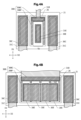
- FIG. 1A is a diagram showing the arrangement of each component of the semiconductor device according to the first embodiment in a plan view
- FIG. 1B is a cross-sectional view taken along the dashed-dotted line 1B-1B in FIG. 1A
- 2A and 2B are plan views showing the arrangement of a base electrode, an emitter electrode, and a collector electrode of two samples to be evaluated.
- FIG. 3 is a graph showing the measurement results of the fracture boundaries of the samples shown in FIGS. 2A and 2B.
- 4A and 4B are diagrams showing the arrangement of components of a semiconductor device according to a comparative example in a plan view.
- FIG. 5 is a diagram showing the arrangement of each component of a semiconductor device according to a comparative example in a plan view.
- FIG. 6A and 6B are schematic diagrams showing the positional relationship between one emitter electrode and one base finger adjacent thereto in plan view.
- 7A and 7B are plan views showing the arrangement and shape of four emitter electrodes.
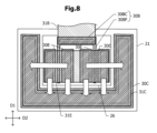
- FIG. 8 is a diagram showing the arrangement of each component of the semiconductor device according to the second embodiment in a plan view.
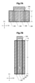
- FIG. 9A is a diagram showing the arrangement of each component of the semiconductor device according to the third embodiment in a plan view, and FIG. 9B is a cross-sectional view taken along the dashed-dotted line 9B-9B in FIG. 9A.
- FIG. 10A is a diagram showing the arrangement of each component of the semiconductor device according to the fourth embodiment in a plan view, and FIG.
- FIG. 10B is a cross-sectional view taken along the dashed-dotted line 10B-10B in FIG. 10A.
- FIG. 11 is a schematic diagram showing the positional relationship in plan view of the emitter electrode and base finger of the semiconductor device according to the fourth example.
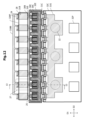
- FIG. 12 is a diagram showing the arrangement of the components of the high frequency power amplifier according to the fifth embodiment in a plan view.
- FIG. 13 is a sectional view taken along the dashed line 13--13 in FIG.
- FIG. 14 is an equivalent circuit diagram of one cell of the high frequency power amplifier according to the fifth embodiment.
- FIG. 15 is a diagram showing the arrangement of each component of the high frequency power amplifier according to the sixth embodiment in a plan view.
- FIG. 16 is a diagram showing the arrangement of each component of the high frequency power amplifier according to the seventh embodiment in a plan view.
- FIG. 17 is a sectional view taken along the dashed line 17--17 in FIG.
- FIG. 18 is a block diagram of a high frequency amplification circuit according to the eighth embodiment.
- FIG. 19 is a diagram showing the arrangement of each component within the substrate of the high frequency amplifier circuit according to the eighth embodiment.
- FIG. 20 is a schematic cross-sectional view of a high frequency front end module according to the eighth embodiment.
- FIG. 1A A semiconductor device according to a first embodiment will be described with reference to FIGS. 1A to 5.
- FIG. 1A A semiconductor device according to a first embodiment will be described with reference to FIGS. 1A to 5.
- FIG. 1A A semiconductor device according to a first embodiment will be described with reference to FIGS. 1A to 5.
- FIG. 1A is a diagram showing the arrangement of each component of the semiconductor device according to the first example in a plan view
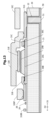
- FIG. 1B is a cross-sectional view taken along the dashed-dotted line 1B-1B in FIG. 1A
- a sub-collector layer 21 having n-type conductivity is disposed in a part of the upper surface, which is one surface, of a substrate 20 made of a semi-insulating semiconductor.
- viewing the top surface of the substrate 20 from a direction perpendicular to the top surface is referred to as a plan view.
- the electrodes in contact with the semiconductor region are hatched relatively thickly upward to the right, and the first layer wiring above them is hatched relatively lightly downwardly to the right.
- a transistor 25 is arranged on a part of the sub-collector layer 21.
- the transistor 25 includes a collector layer 25C, a base layer 25B, and four emitter layers 25E, which are stacked in order from the subcollector layer 21.
- the sub-collector layer 21 and collector layer 25C are formed of n-type GaAs
- the base layer 25B is formed of p-type GaAs
- the emitter layer 25E is formed of n-type InGaP. That is, transistor 25 is a heterojunction bipolar transistor.
- the laminated structure of the collector layer 25C and the base layer 25B is referred to as a collector mesa 26.
- Each of the four emitter layers 25E has a long shape in one direction in plan view. Within the upper surface of the substrate 20, the longitudinal direction of the emitter layer 25E is referred to as a first direction D1, and the direction orthogonal to the first direction D1 is referred to as a second direction D2.
- the four emitter layers 25E are arranged in parallel in the second direction D2 at intervals from each other.
- Emitter electrodes 30E are arranged on each of the emitter layers 25E.
- the emitter electrode 30E has substantially the same shape and the same size as the emitter layer 25E, and substantially overlaps with the emitter layer 25E. That is, the area of the emitter electrode 30E in plan view can be considered to be approximately equal to the area of the emitter-base junction interface.
- Emitter electrode 30E is electrically connected to emitter layer 25E.
- “electrically connected” means connected approximately in accordance with Ohm's law. In the example shown in FIG. 1B, the crystal plane of the base layer 25B in the region where the emitter layer 25E is not arranged is exposed, but a ledge structure that does not expose this crystal plane may be adopted.
- Two collector electrodes 30C are arranged on the upper surface of the sub-collector layer 21 so as to sandwich the collector mesa 26 in the second direction D2 in plan view.
- the collector electrode 30C is electrically connected to the collector layer 25C via the sub-collector layer 21.
- the base electrode 30B includes two base fingers 30BF and a base contact portion 30BC that interconnects the two base fingers 30BF.
- Base electrode 30B is electrically connected to base layer 25B.
- each of the base fingers 30BF has a long shape in the first direction D1, and is arranged side by side in the second direction D2. That is, four emitter electrodes 30E and two base fingers 30BF are arranged side by side in the second direction D2.
- the area between the two base fingers 30BF will be referred to as the inter-base finger area 40.
- emitter electrodes 30E are arranged at both ends in the second direction D2, and are arranged in one inter-base finger region 40 in the second direction D2. Two emitter electrodes 30E are arranged.
- the base contact portion 30BC connects both ends of the two base fingers 30BF.
- the four emitter electrodes 30E and the base electrode 30B are included in the collector mesa 26 in plan view.
- a collector wiring 31C, an emitter wiring 31E, and a base wiring 31B are arranged in the first wiring layer. A portion of the collector wiring 31C overlaps with the collector electrode 30C in plan view.
- the collector wiring 31C is connected to the collector electrode 30C through an opening H2 arranged in an overlapping region with the collector electrode 30C.
- the collector wiring 31C extends from the overlapping region with the collector electrode 30C to one side (lower side in FIG. 1A) in the second direction D2.
- a portion of the base wiring 31B overlaps with the base contact portion 30BC of the base electrode 30B in plan view.
- the base wiring 31B is connected to the base contact portion 30BC through an opening H3 arranged in an overlapping region with the base contact portion 30BC.
- the base wiring 31B extends from the overlapping region with the base contact portion 30BC to one side (upper side in FIG. 1A) in the second direction D2.
- the collector wiring 31C and the base wiring 31B extend in opposite directions.
- the emitter wiring 31E is arranged so as to overlap the four emitter electrodes 30E in plan view.
- the emitter wiring 31E is connected to the four emitter electrodes 30E through openings H1 arranged in respective overlapping regions with the four emitter electrodes 30E.
- An emitter wiring 32E is arranged in the second wiring layer.
- the second-layer emitter wiring 32E overlaps the first-layer emitter wiring 31E in plan view and is connected to the first-layer emitter wiring 31E.
- An emitter external connection terminal 33E is arranged on the second layer emitter wiring 32E, and a solder 34 is placed on top of the emitter external connection terminal 33E.
- a Cu pillar bump is used as the external connection terminal 33E. Note that instead of the Cu pillar bumps, Au bumps, solder ball bumps, etc. may be used.
- FIGS. 2A and 2B are plan views showing the arrangement of the base electrode 30B, emitter electrode 30E, and collector electrode 30C of the two samples. In FIGS. 2A and 2B, these electrodes are hatched. In any sample, the base finger 30BF of the base electrode 30B and the emitter electrode 30E have a long shape in the first direction D1, and the two emitter electrodes 30E are arranged side by side in the second direction D2.
- a base finger 30BF is disposed between two emitter electrodes 30E, and no base finger 30BF is disposed outside the two emitter electrodes 30E.
- three base fingers 30BF are disposed, and an emitter electrode 30E is disposed between each two base fingers 30BF adjacent to each other in the second direction D2.
- a base contact portion 30BC is connected to one end of the base finger 30BF.
- the base finger 30BF is arranged only on one side of each emitter electrode 30E in the width direction (second direction D2).
- base fingers 30BF are arranged on both sides of each emitter electrode 30E in the width direction.
- FIG. 3 is a graph showing the measurement results of the breakdown voltage of the samples shown in FIGS. 2A and 2B.
- the horizontal axis represents collector voltage, and the vertical axis represents collector current.
- the solid line indicates the fracture boundary of the sample shown in FIG. 2A
- the dashed line indicates the fracture boundary of the sample shown in FIG. 2B.
- the breakdown boundary on the high voltage side of the sample in FIG. 2B was about 2V to 3V lower than the breakdown boundary on the high voltage side of the sample in FIG. 2A.
- FIGS. 4A, 4B, and 5 are diagrams showing the arrangement of each component of a semiconductor device according to a comparative example in a plan view.
- the electrodes in contact with the semiconductor region are hatched with relatively dark upward-sloping hatching, and the first layer wiring above them is hatched with relatively light downward-sloping hatching. is marked with hatching.
- each component of the semiconductor device according to the comparative example shown in FIGS. 4A, 4B, and 5 has the same reference numeral as the corresponding component of the semiconductor device according to the first embodiment shown in FIG. 1A. The reference sign is attached.
- two base fingers 30BF are arranged in the collector mesa 26 in plan view, and one emitter electrode 30E is arranged in the region 40 between the base fingers.
- the collector base junction area is denoted as Scb
- the emitter base junction area is denoted as Seb.
- the ratio of the collector base junction area Scb to the emitter base junction area Seb (Scb/Seb) is 1, but since it is necessary to secure an area for arranging the base finger 30BF, Scb/Seb is 1. It becomes bigger. In order to bring Scb/Seb close to 1, it is preferable to make the area of the region occupied by the base finger 30BF smaller than the emitter-base junction area Seb.
- five base fingers 30BF are arranged for four emitter electrodes 30E. Therefore, Scb/Seb of the comparative example shown in FIG.
- the comparative example shown in FIG. 4B is preferable to the comparative example shown in FIG. 4A from the viewpoint of reducing the ratio of the area of the collector-base junction interface to the area of the emitter electrode 30E in plan view.
- the comparative example shown in FIG. 4B since the base fingers 30BF are arranged on both sides of each emitter electrode 30E in the width direction, the evaluation experiment described with reference to the drawings from FIG. 2A to FIG. As a result, the breakdown voltage decreases.
- the two outermost base fingers 30BF of the comparative example shown in FIG. 4B are removed.
- three base fingers 30BF are arranged for four emitter electrodes 30E, and the number of base fingers 30BF for one emitter electrode 30E is smaller than in the case of FIG. 4B.
- the ratio of the area of the collector-base bonding interface to the area of the electrode 30E in plan view is smaller than that of the comparative example shown in FIG. 4B.
- the base finger 30BF is disposed only on one side in the width direction with respect to the outermost emitter electrode 30E, and the base finger 30BF is disposed on only one side in the width direction with respect to the outermost emitter electrode 30E.
- Base fingers 30BF are arranged on both sides. Therefore, variations in operating conditions occur between the emitter electrodes 30E, and variations in emitter current density increase.
- the base finger 30BF when focusing on each emitter electrode 30E, the base finger 30BF is arranged adjacent to only one side of the emitter electrode 30E in the width direction. Therefore, variations in operating conditions among the emitter electrodes 30E are reduced, and variations in emitter current density are also reduced. As a result, thermal uniformity is maintained and thermal runaway is less likely to occur.
- each of the emitter electrodes 30E is different from the comparative example shown in FIG. 2A.
- the emitter electrode 30E of the semiconductor device operates under almost the same operating conditions as the emitter electrode 30E of the semiconductor device. Therefore, the breakdown voltage can be increased as shown in FIG. 3, compared to a configuration in which base fingers 30BF are arranged on both sides of each emitter electrode 30E in the width direction.
- the first embodiment (FIG. 1A) two base fingers 30BF are arranged for four emitter electrodes 30E. That is, the number of base fingers 30BF for one emitter electrode 30E is 1/2, which is fewer than in the comparative examples shown in FIGS. 4B and 5. This makes it possible to reduce the ratio of the area of the collector-base junction interface to the area of the emitter electrode 30E in a plan view.
- the first embodiment is also superior to the comparative examples shown in FIGS. 4B and 5 in terms of reducing the collector-base junction capacitance Cbc relative to the area of the emitter electrode 30E in a plan view. This makes it possible to suppress the decrease in gain caused by the collector-base junction capacitance Cbc.
- FIGS. 6A and 6B are schematic diagrams showing the positional relationship in plan view of one emitter electrode 30E and one base finger 30BF adjacent thereto.
- the emitter electrode 30E is included within the range in which the base finger 30BF is arranged with respect to the first direction D1.
- one edge (the edge indicated by a thick solid line) of the emitter electrode 30E parallel to the first direction D1 faces the base finger 30BF over its entire length.
- the length of the edge of the emitter electrode 30E facing the base finger 30BF is referred to as an opposing length LEB .
- the area of the emitter electrode 30E in plan view is denoted as SE .
- the edge of the emitter electrode 30E parallel to the second direction D2 faces the base contact portion 30BC, but the distance between the emitter electrode 30E and the base contact portion 30BC is smaller than the distance between the emitter electrode 30E and the base finger 30BF. Since it is sufficiently wide, the length of the edge facing the base contact portion 30BC is not included in the facing length LBE here.
- the ratio of the area S E to the opposing length L EB is referred to as the opposing length area ratio R.
- the opposing long area ratio R is preferably 20% or less of the average value of the opposing long area ratio R, and more preferably 10% or less.
- the opposing long area ratio R is the same for all emitter electrodes 30E.
- all the emitter electrodes 30E have the same opposing length L EB and the same area S E . Note that it can be said that they are "the same” even if dimensional variations occur within the tolerance range due to the manufacturing process.
- a part of the emitter electrode 30E extends to the outside of the range where the base finger 30BF is arranged in the first direction D1. That is, only a portion (the portion indicated by the thick solid line) of one edge of the emitter electrode 30E parallel to the first direction D1 faces the base finger 30BF. Of one edge of the emitter electrode 30E parallel to the first direction D1, the length of the portion within the range where the base finger 30BF is arranged with respect to the first direction D1 corresponds to the opposing length LEB .
- Figures 7A and 7B are plan views showing the arrangement and shape of the four emitter electrodes 30E.
- the smallest rectangle that can contain the four emitter electrodes 30E in a plan view is called the minimum inclusive rectangle 41.
- the minimum inclusive rectangle 41 typically, one pair of sides of the minimum inclusive rectangle 41 are parallel to the first direction D1, and the other pair of sides are parallel to the second direction D2.
- the dimension of the minimum inclusive rectangle 41 in the first direction D1 is labeled L1
- the dimension in the second direction D2 is labeled L2.
- the aspect ratio of the minimum containing rectangle 41 is closer to 1 than in the example shown in FIG. 7B.
- the aspect ratio of the minimum enclosing rectangle 41 deviates from 1, that is, when it becomes elongated, variations in temperature tend to occur in the longitudinal direction.
- the transistor 25 tends to undergo thermal runaway.
- the minimum enclosing rectangle 41 be close to a square.
- the ratio of the dimension L2 in the second direction D2 to the dimension L1 in the first direction D1 of the minimum inclusion rectangle 41 is 0.5 or more and 2 or less.
- the number of emitter electrodes 30E and two base fingers 30BF are arranged side by side in the second direction D2, but the number of emitter electrodes 30E is reduced to four.
- the number of base fingers 30BF may be two or more.
- the two emitter electrodes 30E and one base finger 30BF disposed therebetween serve as a repeating unit, and a plurality of repeating units are arranged in line in the second direction D2. That is, the number of emitter electrodes 30E is an even number, and the number of base fingers 30BF is 1/2 of the number of emitter electrodes 30E.
- FIG. 8 is a diagram showing the layout of each component of a semiconductor device according to the second embodiment in a plan view.
- the electrodes in contact with the semiconductor region are hatched with relatively darker lines slanting upward to the right, and the first layer of wiring above them is hatched with relatively lighter lines slanting downward to the right.
- a pair of collector electrodes 30C sandwich the collector mesa 26 in the second direction D2.
- the collector electrode 30C in a plan view, has a row of emitter electrodes 30E and base fingers 30BF lined up in the second direction D2 on both sides of the second direction D2 and on one side of the first direction D1. It is surrounded in a U-shape from the bottom (in FIG. 8).
- the first layer collector wiring 31C also has a U-shape like the collector electrode 30C.
- the excellent effects of the second embodiment will be explained.
- the second embodiment as in the first embodiment, it is possible to suppress a decrease in gain caused by the collector-base junction capacitance Cbc.
- the collector current flows from the emitter electrode 30E to the collector electrode 30C, as shown by the horizontal arrow in FIG.
- the collector current flows not only in the direction of the horizontal arrow shown in FIG. 8 but also in the direction of the vertical arrow. Therefore, the uniformity of the current increases between the plurality of emitter electrodes 30E. As a result, the thermal uniformity is improved, and the effect of suppressing thermal runaway and improving the breakdown voltage is higher than in the case of the first embodiment.
- FIG. 9A is a diagram showing the arrangement of each component of the semiconductor device according to the third example in plan view
- FIG. 9B is a cross-sectional view taken along the dashed-dotted line 9B-9B in FIG. 9A.
- the electrodes in contact with the semiconductor region are hatched relatively darkly upward to the right, and the first layer wiring above them is hatched relatively lightly downwardly to the right. There is.
- the entire base electrode 30B is included in the collector mesa 26 in plan view. That is, the base contact portion 30BC is arranged inside the collector mesa 26 in plan view.
- the base contact portion 30BC is arranged outside the collector mesa 26 in plan view, that is, outside the bonding interface between the base layer 25B and the collector layer 25C.
- an insulating film is disposed between the base electrode 30B and the sub-collector layer 21 in order to prevent the base contact portion 30BC from being electrically connected to the sub-collector layer 21.
- This insulating film is also arranged between base layer 25B and base finger 30BF shown in FIG. 9B. Note that this insulating film is formed after forming the emitter electrode 30E and collector electrode 30C.
- an opening H4 (FIG. 9A) is provided in the insulating film (not shown) disposed between the two.
- the base finger 30BF is electrically connected to the base layer 25B through this opening H4.
- the shape of the base finger 30BF is T-shaped in the cross section shown in FIG. 9B.
- the base finger 30BF crosses the step on the outer periphery of the collector mesa 26 in a plan view, extends to the outside of the collector mesa 26, and is connected to the base contact portion 30BC.
- the advantageous effects of the third embodiment will be described.
- the breakdown voltage is improved and the decrease in gain caused by the collector-base junction capacitance Cbc can be suppressed.
- the area of the collector mesa 26 in a plan view is smaller than that of the first embodiment (FIG. 1A). Therefore, under the condition that the area of the emitter electrode 30E is the same, the collector-base junction capacitance Cbc is smaller. As a result, the effect of suppressing the decrease in gain caused by the collector-base junction capacitance Cbc is further enhanced.
- FIG. 10A is a diagram showing the arrangement of each component of the semiconductor device according to the fourth example in a plan view
- FIG. 10B is a cross-sectional view taken along the dashed-dotted line 10B-10B in FIG. 10A.
- the electrodes in contact with the semiconductor region are hatched relatively darkly upward to the right, and the first layer wiring above them is hatched relatively lightly downwardly to the right. There is.
- the first embodiment two emitter electrodes 30E are arranged in the base inter-finger region 40.
- one emitter electrode 30E and one emitter layer 25E are arranged in the base-finger region 40.
- the dimension in the second direction D2 of the emitter electrode 30E disposed in the inter-base finger region 40 is larger than the dimension in the second direction D2 of each emitter electrode 30E disposed at both ends of the second direction D2.
- the base contact portion 30BC is arranged outside the collector mesa 26 in plan view, similarly to the semiconductor device according to the third embodiment (FIG. 9A).
- the dimensions of the three emitter electrodes 30E in the first direction are the same.
- FIG. 11 is a schematic diagram showing the positional relationship between the emitter electrode 30E and the base finger 30BF in plan view.
- each edge of the emitter electrode 30E the portion facing the base finger 30BF is shown by a thick solid line.
- one edge of a pair of edges parallel to the first direction D1 faces the base finger 30BF.
- both of a pair of edges parallel to the first direction D1 face the base finger 30BF.
- the length of each of the pair of edges parallel to the first direction D1 is equal to the length of each of the pair of edges parallel to the first direction of the emitter electrode 30E at both ends.
- the opposing length of the emitter electrodes 30E at both ends is marked as LEB1 , and the area in plan view is marked as SE1 .
- the opposing lengths L EB1 of the two emitter electrodes 30E at both ends are equal, and the areas S E1 are also equal.
- the opposing length of the emitter electrodes 30E in the base finger inter-region 40 is denoted as LEB2 , and the area in plan view is denoted as SE2 .
- LEB2 The opposing length of the emitter electrodes 30E disposed in the inter-base finger region 40
- SE2 the area in plan view
- both of the two edges parallel to the first direction D1 face the base finger 30BF, so the following equation holds true.
- L EB2 2 x L EB1 ...(2)
- the opposing long area ratio R2 of the emitter electrodes 30E arranged in the base finger inter-region 40 is calculated by the following formula.
- the difference between the maximum value and the minimum value of the opposing long area ratios R 1 and R 2 is preferably 20% or less, and preferably 10% or less, of the average value of the opposing long area ratios R 1 and R 2 . is more preferable.
- the opposing long area ratio R 2 of the emitter electrodes 30E in the base finger inter-region 40 be equal to the opposing long area ratio R 1 of the emitter electrodes 30E at both ends.
- the area S E2 of the emitter electrode 30E in the base-to-finger region 40 is equal to twice the area S E1 of the emitter electrodes 30E at both ends.
- the fourth embodiment As in the first embodiment, it is possible to improve the breakdown voltage and suppress a decrease in gain caused by the collector-base junction capacitance Cbc.
- the first embodiment (FIG. 1B)
- a gap is ensured between the two emitter electrodes 30E in the base-to-finger region 40, but in the fourth embodiment, it is not necessary to ensure this gap. Therefore, compared to the first embodiment, the area of the collector mesa 26 (FIG. 10A) can be made smaller. As a result, it becomes possible to further reduce the collector-base junction capacitance Cbc.
- the fourth embodiment three emitter electrodes 30E are arranged, but four or more emitter electrodes 30E may be arranged.
- the number of base fingers 30BF is one less than the number of emitter electrodes 30E.
- One emitter electrode 30E is arranged in each of the plurality of inter-base finger regions 40.
- two emitter electrodes 30E are arranged in the base finger inter-region 40 as in the first embodiment, and a base as in the fourth embodiment.
- a portion where one emitter electrode 30E is arranged may be mixed in the inter-finger region 40.
- the high frequency power amplifier according to the fifth embodiment includes the semiconductor device according to any one of the first to fourth embodiments.
- FIG. 12 is a diagram showing the arrangement of each component of the high-frequency power amplifier according to the fifth embodiment in a plan view.
- FIG. 13 is a sectional view taken along the dashed line 13--13 in FIG.
- the electrodes in contact with the semiconductor region are hatched relatively thickly upward to the right
- the first layer interconnects are hatched relatively lightly downwardly to the right
- the outlines of the second layer interconnects are indicated relative to each other. It is represented by a thick solid line.
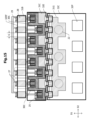
- a plurality of cells 27 are arranged on the upper surface of the substrate 20 in a line in the second direction D2.
- Each of the plurality of cells 27 includes the transistor 25 of the semiconductor device according to the third embodiment (FIGS. 9A and 9B), a collector electrode 30C, an emitter electrode 30E, and a base electrode 30B.
- Each of the plurality of cells 27 further includes an input capacitor 28 and a ballast resistance element 29.
- the structure of the semiconductor device according to the first embodiment, the second embodiment, or the fourth embodiment may be adopted for each of the cells 27.
- the collector electrodes 30C of two cells 27 adjacent in the second direction D2 are continuous with each other.
- a first layer base wiring 31B extends in a first direction (upward in FIG. 12) from the base contact portion 30BC (FIG. 9A) of each of the plurality of cells 27.
- the high frequency signal input wiring 32RF arranged in the second wiring layer intersects with the plurality of base wirings 31B.
- a portion of the base wiring 31B overlapping with the high frequency signal input wiring 32RF is widened compared to other portions, and an input capacitor 28 is formed in the overlapping portion.
- ballast resistance elements 29 overlaps with the tip of the plurality of base wirings 31B, respectively.
- the other end of the ballast resistance element 29 overlaps a part of the common base bias wiring 31BB arranged in the first wiring layer.
- the ballast resistance element 29 is arranged with respect to the base wiring 31B and the base bias wiring 31BB without interposing an interlayer insulating film.
- the second layer emitter wiring 32E includes a plurality of transistors 25 in a plan view.
- the emitter wiring 32E in the second layer is connected to the plurality of emitter wirings 31E in the first layer through via holes provided in the interlayer insulating film.
- the first layer ground wiring 31G is arranged to run parallel to the cell rows of the plurality of cells 27. A portion of the ground wiring 31G overlaps a portion of the second layer emitter wiring 32E, and the two are connected to each other at the overlapped portion.
- a plurality of through via holes 22 passing through the substrate 20 are provided at positions included in the ground wiring 31G in plan view.
- a back electrode 50 is arranged on the back surface of the substrate 20 opposite to the top surface. The back electrode 50 is connected to the ground wiring 31G through the side surface of the through via hole 22. The remaining portion of the through-via hole 22 is filled with a conductive filling member 51 .
- the second layer collector wiring 32C is arranged so as to run parallel to the cell rows of the plurality of cells 27 in plan view. A portion of the second-layer collector wiring 32C overlaps a portion of the first-layer collector wiring 31C, and the two are connected at the overlapped portion. A part of the second layer collector wiring 32C is used as a wire bonding pad 32P.
- FIG. 14 is an equivalent circuit diagram of one cell 27.
- Each cell 27 includes a transistor 25, an input capacitor 28, and a ballast resistance element 29.
- the emitter of the transistor 25 is connected to the ground wiring 31G, and the collector is connected to the collector wiring 32C. Power is supplied to the transistor 25 from the collector wiring 32C.
- the base of the transistor 25 is connected to the high frequency signal input wiring 32RF via the input capacitor 28.
- a high frequency signal is input from the high frequency signal input wiring 32RF to the base of the transistor 25 via the input capacitor 28.
- the base of the transistor 25 is further connected to a base bias wiring 31BB via a ballast resistance element 29.
- a base bias is supplied to the base of the transistor 25 from the base bias wiring 31BB via the ballast resistance element 29.
- each of the plurality of cells 27 includes a transistor 25 having the same configuration as any of the semiconductor devices from the first embodiment to the fourth embodiment. Similar to the semiconductor devices up to the fourth embodiment, it is possible to improve the breakdown voltage and suppress the decrease in gain caused by the collector-base junction capacitance Cbc.
- FIG. 15 is a diagram showing the arrangement of each component of the high-frequency power amplifier according to the sixth embodiment in a plan view.
- the electrodes in contact with the semiconductor region are hatched relatively thickly upward to the right
- the wiring in the first layer is hatched relatively lightly downwardly to the right
- the wiring in the second layer The outline of the wiring is shown by a relatively thick solid line.
- the transistors 25 of each of the plurality of cells 27 are arranged on one straight line parallel to the second direction D2.
- the transistors 25 of each of the plurality of cells 27 are arranged in a staggered manner.
- each of the odd-numbered cells 27 and the even-numbered cells 27 are sequentially numbered starting from 1 from the cell 27 at one end to the cell 27 at the other end in the second direction D2.
- each of the odd-numbered cells 27 and the even-numbered cells 27 The transistors 25 are arranged on one straight line parallel to the second direction D2.
- the transistors 25 of the even-numbered cells 27 are arranged at positions shifted in the first direction D1 with respect to the transistors 25 of the odd-numbered cells 27.
- the transistors 25 of the even-numbered cells 27 are arranged farther than the transistors 25 of the odd-numbered cells 27.
- the amount of deviation in the first direction D1 of the transistor 25 of the even-numbered cell 27 with respect to the transistor 25 of the odd-numbered cell 27 is the dimension of the collector mesa 26 of each transistor 25 (FIG. 1A, FIG. 9A, etc.) in the first direction D1. That's all.
- the dimension in the second direction D2 (hereinafter sometimes referred to as the width) of the collector electrode 30C of the transistor 25 that is farthest from the second layer collector wiring 32C is the size of two adjacent collector electrodes diagonally with respect to the second direction D2. This is slightly smaller than the distance G between the two transistors 25 in the second direction D2, and is sufficiently larger than 1/2 of the distance G.
- the width of the first layer collector wiring 31C that substantially overlaps the collector electrode 30C in plan view is also approximately the same as the width of the collector electrode 30C.
- the first-layer collector wiring 31C is arranged in almost the entire area between the transistors 25 adjacent to each other in the second direction D2 among the transistors 25 that are closer to the second-layer collector wiring 32C when viewed from the second-layer collector wiring 32C.
- the excellent effects of the sixth embodiment will be explained.
- the sixth embodiment as in the fifth embodiment, it is possible to improve the breakdown voltage and suppress a decrease in gain caused by the collector-base junction capacitance Cbc.
- the distribution density of the transistors 25 is lower than that in the fifth embodiment. Therefore, heat dissipation from the transistor 25 can be improved.
- the collector wiring 31C arranged between two transistors 25 adjacent to each other in the second direction D2 is shared by the two transistors 25. Therefore, it can be considered that the area through which the collector current of one transistor 25 flows is substantially limited to a region that is half the width of the collector wiring 31C arranged between the two transistors 25. .
- the collector current of one transistor 25 is connected to the collector wiring 31C, which is disposed at a position sandwiching the transistor 25 that is farthest from the second layer collector wiring 32C in the second direction D2. only flows. Therefore, the width of the collector wiring 31C arranged for the transistor 25 that is farthest from the second layer collector wiring 32C is substantially increased.
- the first layer collector wire 31C is arranged in almost the entire area between the two transistors 25 adjacent to each other in the second direction D2. ing. Therefore, it can be considered that the width of the collector wiring 31C arranged for the transistor 25 that is closer to the second layer collector wiring 32C when viewed from the second layer collector wiring 32C is sufficiently wide.
- the width of the collector wiring 31C arranged for each of the plurality of transistors 25 is wider than that in the fifth embodiment. Therefore, the parasitic resistance of the collector wiring 31C can be substantially reduced.
- the emitter of the transistor 25 is connected to a back electrode 50 arranged on the back surface of the substrate 20, as shown in FIG. 13.
- a wire bonding pad 32P is arranged on the upper surface of the substrate 20. That is, the radio frequency power amplifier according to the sixth embodiment is mounted on the mounting substrate such that the surface on which the transistor 25 is arranged faces away from the mounting substrate (face-up mounting). In contrast, the radio frequency power amplifier according to the seventh embodiment is mounted on the mounting substrate such that the surface on which the transistor 25 is arranged faces the mounting substrate (face-down mounting).
- FIG. 16 is a diagram showing the layout of each component of a radio frequency power amplifier according to the seventh embodiment in a plan view.
- FIG. 17 is a cross-sectional view taken along dashed line 17-17 in FIG. 16.
- electrodes in contact with semiconductor regions are shown with relatively darker hatching slanting upwards to the right
- the first layer wiring is shown with relatively lighter hatching slanting downwards to the right
- the outline of the second layer wiring is shown with a relatively thick solid line.
- the outline of the external connection terminals arranged on the second layer wiring is shown with an even thicker solid line.
- the second layer emitter wiring 32E is arranged so as to include the plurality of transistors 25 in a plan view.
- An emitter external connection terminal 33E is arranged on the second layer emitter wiring 32E.
- the external connection terminal 33E at least partially overlaps all the transistors 25 in plan view.
- a second-layer collector wiring 32C is arranged to run parallel to the second-layer emitter wiring 32E. A portion of the second-layer collector wiring 32C overlaps a portion of the first-layer collector wiring 31C, and the two are connected at the overlapped portion.
- a plurality of collector external connection terminals 33C are arranged on the second layer collector wiring 31C.
- Solder 34 is placed on each of the emitter external connection terminal 33E and the collector external connection terminal 33C.
- Cu pillar bumps are used for the external connection terminals 33E and 33C. Note that instead of the Cu pillar bumps, Au bumps, solder ball bumps, etc. may be used.
- the excellent effects of the seventh embodiment will be explained.
- the seventh embodiment as in the sixth embodiment, it is possible to improve the breakdown voltage and suppress the decrease in gain caused by the collector-base junction capacitance Cbc.
- the emitter external connection terminal 33E functions as a heat dissipation path from the transistor 25 to the mounting board. Therefore, the temperature rise of the transistor 25 during operation can be suppressed.
- the high frequency amplifier circuit according to the eighth embodiment includes the high frequency power amplifier (FIGS. 16 and 17) according to the seventh embodiment.
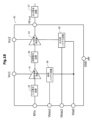
- FIG. 18 is a block diagram of a high frequency amplification circuit 60 according to the eighth embodiment.
- the high frequency amplifier circuit 60 according to the eighth embodiment includes a first stage amplifier circuit 61, an output stage amplifier circuit 62, an input matching circuit 65, an interstage matching circuit 66, a first stage bias circuit 68, and an output stage bias circuit 69.
- the high frequency amplification circuit 60 according to the eighth embodiment has external connection terminals configured with bumps: a high frequency signal input terminal RFin, a high frequency signal output terminal RFout, a first stage bias control terminal Vbias1, an output stage bias control terminal Vbias2, and a power supply terminal. It includes Vcc1, Vcc2, a bias power supply terminal Vbatt, and a ground terminal GND. Note that although the block diagram of FIG. 18 shows only one ground terminal GND, a plurality of ground terminals GND are actually arranged.
- a high frequency signal input from the high frequency signal input terminal RFin is input to the first stage amplifier circuit 61 via the input matching circuit 65.
- the high frequency signal amplified by the first stage amplifier circuit 61 is input to the output stage amplifier circuit 62 via the interstage matching circuit 66.
- the high frequency signal amplified by the output stage amplifier circuit 62 is output from the high frequency signal output terminal RFout.
- the high frequency power amplifier according to the seventh embodiment (FIGS. 16 and 17) is used in the output stage amplifier circuit 62.
- An output matching circuit 67 is connected to the high frequency signal output terminal RFout.
- a power supply voltage is applied from the power supply terminals Vcc1 and Vcc2 to the first stage amplifier circuit 61 and the output stage amplifier circuit 62, respectively.
- Bias power is supplied from the bias power supply terminal Vbatt to the first stage bias circuit 68 and the output stage bias circuit 69.
- the first stage bias circuit 68 supplies bias to the first stage amplifier circuit 61 based on the bias control signal input to the first stage bias control terminal Vbias1.
- the output stage bias circuit 69 supplies bias to the output stage amplifier circuit 62 based on the bias control signal input to the output stage bias control terminal Vbias2.
- FIG. 19 is a diagram showing the arrangement of each component within the substrate of the high frequency amplification circuit 60 according to the eighth embodiment.
- main wirings in the first and second layers are hatched.
- An output stage amplifier circuit 62 is arranged at a position overlapping with the emitter external connection terminal 33E.
- one external connection terminal 33E is arranged for eight transistors 25, but in the eighth embodiment, 14 transistors 25 are divided into two groups, External connection terminals 33E are arranged for each of the two sets.
- three external connection terminals 33C are arranged for eight transistors 25, but in the eighth embodiment, one external connection terminal 33C is arranged for fourteen transistors 25.
- a connection terminal 33C is arranged.
- the external connection terminal 33C corresponds to the power supply terminal Vcc2 (FIG. 18) and the high frequency signal output terminal RFout (FIG. 18).
- first stage amplifier circuit 61 an input matching circuit 65, an interstage matching circuit 66, a first stage bias circuit 68, an output stage bias circuit 69, a high frequency signal input terminal RFin, a power supply terminal Vcc1, and a bias power supply terminal Vbatt. , an initial stage bias control terminal Vbias1, and an output stage bias control terminal Vbias2. Further, a ground terminal GND and the like connected to the emitters of the plurality of transistors included in the first stage amplifier circuit 61 are arranged.
- FIG. 20 is a schematic cross-sectional view of a high frequency front end module according to the eighth embodiment.
- an emitter external connection terminal 33E On one side of the high frequency amplifier circuit 60, an emitter external connection terminal 33E, a collector external connection terminal 33C, etc. are arranged.
- a plurality of lands 74 are arranged on the mounting surface of the module board 70.
- External connection terminals 33E and 33C of high frequency amplification circuit 60 are connected to lands 74 of module board 70 with solder 80.
- the high frequency amplification circuit 60 is provided with a plurality of external connection terminals for power supply and signals (FIG. 19). These external connection terminals are also connected to corresponding lands on the module board 70 by solder.
- a plurality of surface mount components 75 such as inductors and capacitors are mounted on the mounting surface of the module board 70. Some of these surface mount components 75 constitute an output matching assembly 67 (FIG. 18).
- a ground plane 72 is arranged on the inner layer of the module board 70 and on the surface opposite to the mounting surface (hereinafter referred to as the back surface).
- a plurality of vias 73 are provided extending from a ground land 74 arranged on the mounting surface to a ground plane 72 on the back surface.
- the high frequency amplification circuit (FIGS. 16 and 17) according to the seventh embodiment is used in the output stage amplification circuit 62 (FIG. 18) of the high frequency amplification circuit 60. Therefore, similarly to the fifth embodiment, it is possible to improve the breakdown voltage of the transistor 25 of the output stage amplifier circuit 62 and to suppress a decrease in gain caused by the collector-base junction capacitance Cbc.
Landscapes
- Engineering & Computer Science (AREA)
- Power Engineering (AREA)
- Microelectronics & Electronic Packaging (AREA)
- Bipolar Transistors (AREA)
- Electrodes Of Semiconductors (AREA)
Abstract
Description
基板と、
前記基板の一方の面である上面の上に順番に積層されたコレクタ層、ベース層、及びエミッタ層を含むトランジスタと、
前記エミッタ層に電気的に接続された4つ以上のエミッタ電極と、
前記ベース層に電気的に接続された2つ以上のベースフィンガを含むベース電極と、
前記コレクタ層に電気的に接続されたコレクタ電極と
を備えており、
前記エミッタ電極の各々、及び前記ベースフィンガの各々は、前記基板の前記上面内の第1方向に長い形状を有し、
前記エミッタ電極及び前記ベースフィンガは、前記基板の前記上面内で前記第1方向と直交する第2方向に並んで配置されており、
前記第2方向に並ぶ4つ以上の前記エミッタ電極及び2つ以上の前記ベースフィンガの列において、前記第2方向の両端には、それぞれ前記エミッタ電極が配置されており、
前記第2方向に隣り合う2つの前記ベースフィンガの間のベースフィンガ間領域のうち、少なくとも1つの前記ベースフィンガ間領域には、前記第2方向に並ぶ2つの前記エミッタ電極が配置されており、
複数の前記エミッタ電極の各々の隣に配置された1つまたは2つの前記ベースフィンガに対向する前記エミッタ電極の縁の長さに対する前記エミッタ電極の平面視における面積の比を対向長面積比と定義したとき、複数の前記エミッタ電極のそれぞれの前記対向長面積比の最大値と最小値との差が、前記対向長面積比の平均値の20%以下である半導体装置が提供される。
基板の一方の面である上面の上に順番に積層されたコレクタ層、ベース層、及びエミッタ層を含むトランジスタと、
前記エミッタ層に電気的に接続された3つのエミッタ電極と、
前記ベース層に電気的に接続された2つのベースフィンガを含むベース電極と
前記コレクタ層に電気的に接続されたコレクタ電極と
を備えており、
前記エミッタ電極の各々、及び前記ベースフィンガの各々は、前記基板の前記上面内の第1方向に長い形状を有し、
3つの前記エミッタ電極及び2つの前記ベースフィンガは、前記基板の前記上面内で前記第1方向と直交する第2方向に、前記エミッタ電極、前記ベースフィンガ、前記エミッタ電極、前記ベースフィンガ、前記エミッタ電極の順に並んで配置されており、
複数の前記エミッタ電極の各々の隣に配置された1つまたは2つの前記ベースフィンガに対向する前記エミッタ電極の縁の長さに対する前記エミッタ電極の平面視における面積の比を対向長面積比と定義したとき、複数の前記エミッタ電極のそれぞれの前記対向長面積比の最大値と最小値との差が、前記対向長面積比の平均値の20%以下であり、
平面視において、3つの前記エミッタ電極を包含する最小包含長方形の前記第1方向の寸法に対する前記第2方向の寸法の比が0.5以上2以下である半導体装置が提供される。
前記基板の前記上面に、前記第2方向に並んで配置された複数の前記半導体装置と、
前記複数の半導体装置の前記エミッタ電極を接続するエミッタ配線と、
高周波信号入力配線と、
前記複数の半導体装置の各々の前記ベース電極と、前記高周波信号入力配線とを接続する入力キャパシタと
を備え、
前記複数の半導体装置の前記コレクタ電極は相互に連続している高周波電力増幅器が提供される。
図1Aから図5までの図面を参照して第1実施例による半導体装置について説明する。
第1実施例では、1つのトランジスタ25(図1B)において、4つのエミッタ電極30Eと2つのベースフィンガ30BFとが第2方向D2に並んで配置されているが、エミッタ電極30Eの個数を4個以上にし、ベースフィンガ30BFの本数を2本以上にしてもよい。このとき、2つのエミッタ電極30Eと、その間に配置された1本のベースフィンガ30BFとが繰り返し単位となって、複数の繰り返し単位が第2方向D2に並んで配置される。すなわち、エミッタ電極30Eの個数は偶数であり、ベースフィンガ30BFの本数はエミッタ電極30Eの個数の1/2である。
次に、図8を参照して第2実施例による半導体装置について説明する。以下、図1Aから図7Bまでの図面を参照して説明した第1実施例による半導体装置と共通の構成については説明を省略する。
第2実施例においても第1実施例と同様に、コレクタベース間接合容量Cbcに起因するゲインの低下を抑制することができる。
次に、図9A及び図9Bを参照して第3実施例による半導体装置について説明する。以下、図1Aから図7Bまでの図面を参照して説明した第1実施例による半導体装置と共通の構成については説明を省略する。
第3実施例においても第1実施例と同様に、破壊耐圧を向上させるとともに、コレクタベース間接合容量Cbcに起因するゲインの低下を抑制することができる。第3実施例では、第1実施例(図1A)と比べてコレクタメサ26の平面視における面積が小さい。このため、エミッタ電極30Eの面積が同一の条件の下で、コレクタベース間接合容量Cbcがより小さくなる。その結果、コレクタベース間接合容量Cbcに起因するゲインの低下を抑制する効果がより高まる。
次に、図10Aから図11までの図面を参照して、第4実施例による半導体装置について説明する。以下、図1Aから図7Bまでの図面を参照して説明した第1実施例による半導体装置と共通の構成については説明を省略する。
R1=SE1/LEB1・・・(1)
LEB2=2×LEB1・・・(2)
R2=SE2/LEB2=SE2/(2×LEB1)・・・(3)
第4実施例においても第1実施例と同様に、破壊耐圧を向上させるとともに、コレクタベース間接合容量Cbcに起因するゲインの低下を抑制することができる。第1実施例(図1B)では、ベースフィンガ間領域40内の2つのエミッタ電極30Eの間に間隙が確保されているが、第4実施例では、この間隙を確保する必要がない。このため、第1実施例と比べて、コレクタメサ26(図10A)の面積をより小さくすることができる。その結果、コレクタベース間接合容量Cbcをより小さくすることが可能になる。
第4実施例では、エミッタ電極30Eを3個配置しているが、4個以上配置してもよい。この場合、ベースフィンガ30BFの本数は、エミッタ電極30Eの個数より1つだけ少ない本数になる。複数のベースフィンガ間領域40にエミッタ電極30Eが1つずつ配置される。
次に、図12から図14までの図面を参照して第5実施例による高周波電力増幅器について説明する。第5実施例による高周波電力増幅器には、第1実施例から第4実施例までのいずれかの実施例による半導体装置が含まれる。
第5実施例においては、複数のセル27のそれぞれが、第1実施例から第4実施例までのいずれかの半導体装置と同一の構成のトランジスタ25を含んでいるため、第1実施例から第4実施例までの半導体装置と同様に、破壊耐圧を向上させるとともに、コレクタベース間接合容量Cbcに起因するゲインの低下を抑制することができる。
次に、図15を参照して第6実施例による高周波電力増幅器について説明する。以下、図12から図14までの図面を参照して説明した第5実施例による高周波電力増幅器と共通の構成については説明を省略する。
第6実施例においても第5実施例と同様に、破壊耐圧を向上させるとともに、コレクタベース間接合容量Cbcに起因するゲインの低下を抑制することができる。第6実施例では、第5実施例と比べてトランジスタ25の分布密度が低い。このため、トランジスタ25からの放熱性を高めることができる。
次に、図16及び図17を参照して第7実施例による高周波電力増幅器について説明する。以下、図15を参照して説明した第6実施例による高周波電力増幅器と共通の構成については説明を省略する。
第7実施例においても第6実施例と同様に、破壊耐圧を向上させるとともに、コレクタベース間接合容量Cbcに起因するゲインの低下を抑制することができる。第7実施例では、エミッタ用の外部接続端子33Eがトランジスタ25から実装基板に向かう放熱経路として機能する。このため、動作時におけるトランジスタ25の温度上昇を抑制することができる。
次に、図18、図19、及び図20を参照して、第8実施例による高周波増幅回路及び高周波フロントエンドモジュールについて説明する。第8実施例による高周波増幅回路は、第7実施例による高周波電力増幅器(図16、図17)を含む。
第8実施例では、高周波増幅回路60の出力段増幅回路62(図18)に、第7実施例による高周波増幅回路(図16、図17)が用いられている。このため、第5実施例と同様に、出力段増幅回路62のトランジスタ25の破壊耐圧を向上させるとともに、コレクタベース間接合容量Cbcに起因するゲインの低下を抑制することができる。
21 サブコレクタ層
22 貫通バイアホール
25 トランジスタ
25B ベース層
25C コレクタ層
25E エミッタ層
26 コレクタメサ
27 セル
28 入力キャパシタ
29 バラスト抵抗素子
30B ベース電極
30BC ベースコンタクト部
30BF ベースフィンガ
30C コレクタ電極
30E エミッタ電極
31B 1層目のベース配線
31BB ベースバイアス配線
31C 1層目のコレクタ配線
31E 1層目のエミッタ配線
31G 1層目のグランド配線
32C 2層目のコレクタ配線
32E 2層目のエミッタ配線
32P ワイヤボンディング用のパッド
32RF 2層目の高周波信号入力配線
33C コレクタ用の外部接続端子
33E エミッタ用の外部接続端子
34 ハンダ
40 ベースフィンガ間領域
41 最小包含長方形
50 裏面電極
51 充填部材
60 高周波増幅回路
61 初段増幅回路
62 出力段増幅回路(高周波信号電力増幅回路)
65 入力整合回路
66 段間整合回路
68 初段バイアス回路
69 出力段バイアス回路
70 モジュール基板
72 グランドプレーン
73 ビア
74 ランド
75 表面実装部品
80 ハンダ
Claims (10)
- 基板と、
前記基板の一方の面である上面の上に順番に積層されたコレクタ層、ベース層、及びエミッタ層を含むトランジスタと、
前記エミッタ層に電気的に接続された4つ以上のエミッタ電極と、
前記ベース層に電気的に接続された2つ以上のベースフィンガを含むベース電極と、
前記コレクタ層に電気的に接続されたコレクタ電極と
を備えており、
前記エミッタ電極の各々、及び前記ベースフィンガの各々は、前記基板の前記上面内の第1方向に長い形状を有し、
前記エミッタ電極及び前記ベースフィンガは、前記基板の前記上面内で前記第1方向と直交する第2方向に並んで配置されており、
前記第2方向に並ぶ4つ以上の前記エミッタ電極及び2つ以上の前記ベースフィンガの列において、前記第2方向の両端には、それぞれ前記エミッタ電極が配置されており、
前記第2方向に隣り合う2つの前記ベースフィンガの間のベースフィンガ間領域のうち、少なくとも1つの前記ベースフィンガ間領域には、前記第2方向に並ぶ2つの前記エミッタ電極が配置されており、
複数の前記エミッタ電極の各々の隣に配置された1つまたは2つの前記ベースフィンガに対向する前記エミッタ電極の縁の長さに対する前記エミッタ電極の平面視における面積の比を対向長面積比と定義したとき、複数の前記エミッタ電極のそれぞれの前記対向長面積比の最大値と最小値との差が、前記対向長面積比の平均値の20%以下である半導体装置。 - 4つ以上の前記エミッタ電極の平面視における面積が同一である請求項1に記載の半導体装置。
- 基板の一方の面である上面の上に順番に積層されたコレクタ層、ベース層、及びエミッタ層を含むトランジスタと、
前記エミッタ層に電気的に接続された3つのエミッタ電極と、
前記ベース層に電気的に接続された2つのベースフィンガを含むベース電極と
前記コレクタ層に電気的に接続されたコレクタ電極と
を備えており、
前記エミッタ電極の各々、及び前記ベースフィンガの各々は、前記基板の前記上面内の第1方向に長い形状を有し、
3つの前記エミッタ電極及び2つの前記ベースフィンガは、前記基板の前記上面内で前記第1方向と直交する第2方向に、前記エミッタ電極、前記ベースフィンガ、前記エミッタ電極、前記ベースフィンガ、前記エミッタ電極の順に並んで配置されており、
複数の前記エミッタ電極の各々の隣に配置された1つまたは2つの前記ベースフィンガに対向する前記エミッタ電極の縁の長さに対する前記エミッタ電極の平面視における面積の比を対向長面積比と定義したとき、複数の前記エミッタ電極のそれぞれの前記対向長面積比の最大値と最小値との差が、前記対向長面積比の平均値の20%以下であり、
平面視において、3つの前記エミッタ電極を包含する最小包含長方形の前記第1方向の寸法に対する前記第2方向の寸法の比が0.5以上2以下である半導体装置。 - 平面視において、前記コレクタ電極は、前記第2方向に並ぶ前記エミッタ電極及び前記ベースフィンガの列を、前記第2方向の両側、及び前記第1方向の片側からU字状に囲んでいる請求項1乃至3のいずれか1項に記載の半導体装置。
- 前記ベース電極は、平面視において、前記ベース層と前記コレクタ層との接合界面の外側で、複数の前記ベースフィンガを相互に接続している請求項1乃至4のいずれか1項に記載の半導体装置。
- 前記ベースフィンガの本数が2本であり、
平面視において、複数の前記エミッタ電極を包含する最小包含長方形の前記第1方向の寸法に対する前記第2方向の寸法の比が、0.5以上2以下である請求項1または2に記載の半導体装置。 - 前記トランジスタは、ヘテロ接合バイポーラトランジスタである請求項1乃至6のいずれか1項に記載の半導体装置。
- 前記基板の前記上面に、前記第2方向に並んで配置された請求項1乃至7のいずれか1項に記載の複数の半導体装置と、
前記複数の半導体装置の前記エミッタ電極を接続するエミッタ配線と、
高周波信号入力配線と、
前記複数の半導体装置の各々の前記ベース電極と、前記高周波信号入力配線とを接続する入力キャパシタと
を備え、
前記複数の半導体装置の前記コレクタ電極は相互に連続している高周波電力増幅器。 - 前記基板の前記上面とは反対側の下面に配置された裏面電極を、さらに備え、
前記基板に、貫通バイアホールが設けられており、
前記裏面電極は、前記貫通バイアホールを通って前記エミッタ配線に電気的に接続されている請求項8に記載の高周波電力増幅器。 - 前記基板の前記上面の上に配置され、前記エミッタ配線に電気的に接続された外部接続端子を、さらに備えた請求項8に記載の高周波電力増幅器。
Priority Applications (2)
| Application Number | Priority Date | Filing Date | Title |
|---|---|---|---|
| CN202380067019.5A CN119968933A (zh) | 2022-09-20 | 2023-08-23 | 半导体装置和高频功率放大器 |
| US19/081,659 US20250212432A1 (en) | 2022-09-20 | 2025-03-17 | Semiconductor device and radio frequency power amplifier |
Applications Claiming Priority (2)
| Application Number | Priority Date | Filing Date | Title |
|---|---|---|---|
| JP2022-149477 | 2022-09-20 | ||
| JP2022149477 | 2022-09-20 |
Related Child Applications (1)
| Application Number | Title | Priority Date | Filing Date |
|---|---|---|---|
| US19/081,659 Continuation US20250212432A1 (en) | 2022-09-20 | 2025-03-17 | Semiconductor device and radio frequency power amplifier |
Publications (1)
| Publication Number | Publication Date |
|---|---|
| WO2024062829A1 true WO2024062829A1 (ja) | 2024-03-28 |
Family
ID=90454099
Family Applications (1)
| Application Number | Title | Priority Date | Filing Date |
|---|---|---|---|
| PCT/JP2023/030322 Ceased WO2024062829A1 (ja) | 2022-09-20 | 2023-08-23 | 半導体装置及び高周波電力増幅器 |
Country Status (4)
| Country | Link |
|---|---|
| US (1) | US20250212432A1 (ja) |
| CN (1) | CN119968933A (ja) |
| TW (1) | TWI863401B (ja) |
| WO (1) | WO2024062829A1 (ja) |
Families Citing this family (1)
| Publication number | Priority date | Publication date | Assignee | Title |
|---|---|---|---|---|
| JP2025116469A (ja) * | 2024-01-29 | 2025-08-08 | 三菱電機株式会社 | 高周波用トランジスタ |
Citations (4)
| Publication number | Priority date | Publication date | Assignee | Title |
|---|---|---|---|---|
| JP2002076014A (ja) * | 2000-08-30 | 2002-03-15 | Mitsubishi Electric Corp | 高周波用半導体装置 |
| JP2007035809A (ja) * | 2005-07-26 | 2007-02-08 | Sony Corp | 半導体装置及びその製造方法 |
| JP2021132100A (ja) * | 2020-02-19 | 2021-09-09 | 株式会社村田製作所 | 高周波電力増幅素子 |
| JP2022080639A (ja) * | 2020-11-18 | 2022-05-30 | 株式会社村田製作所 | 半導体装置 |
Family Cites Families (1)
| Publication number | Priority date | Publication date | Assignee | Title |
|---|---|---|---|---|
| JP7625825B2 (ja) * | 2020-10-21 | 2025-02-04 | 株式会社村田製作所 | 半導体装置 |
-
2023
- 2023-07-03 TW TW112124755A patent/TWI863401B/zh active
- 2023-08-23 CN CN202380067019.5A patent/CN119968933A/zh active Pending
- 2023-08-23 WO PCT/JP2023/030322 patent/WO2024062829A1/ja not_active Ceased
-
2025
- 2025-03-17 US US19/081,659 patent/US20250212432A1/en active Pending
Patent Citations (4)
| Publication number | Priority date | Publication date | Assignee | Title |
|---|---|---|---|---|
| JP2002076014A (ja) * | 2000-08-30 | 2002-03-15 | Mitsubishi Electric Corp | 高周波用半導体装置 |
| JP2007035809A (ja) * | 2005-07-26 | 2007-02-08 | Sony Corp | 半導体装置及びその製造方法 |
| JP2021132100A (ja) * | 2020-02-19 | 2021-09-09 | 株式会社村田製作所 | 高周波電力増幅素子 |
| JP2022080639A (ja) * | 2020-11-18 | 2022-05-30 | 株式会社村田製作所 | 半導体装置 |
Also Published As
| Publication number | Publication date |
|---|---|
| CN119968933A (zh) | 2025-05-09 |
| TW202414601A (zh) | 2024-04-01 |
| TWI863401B (zh) | 2024-11-21 |
| US20250212432A1 (en) | 2025-06-26 |
Similar Documents
| Publication | Publication Date | Title |
|---|---|---|
| CN109994440B (zh) | 半导体装置 | |
| TWI752598B (zh) | 放大電路之單位單元及功率放大器模組 | |
| US10868155B2 (en) | Compound semiconductor device | |
| CN110912523A (zh) | 高频功率放大器以及功率放大模块 | |
| JP2019220668A (ja) | 半導体装置 | |
| JP2020048184A (ja) | 高周波電力増幅器及び電力増幅モジュール | |
| US20240321975A1 (en) | Bipolar transistor and semiconductor | |
| US20250212432A1 (en) | Semiconductor device and radio frequency power amplifier | |
| TWI747145B (zh) | 半導體裝置及放大器模組 | |
| CN111683471B (zh) | 多层布线基板 | |
| TWI754492B (zh) | 高頻功率放大元件 | |
| US20240014296A1 (en) | Semiconductor device and semiconductor module | |
| TWI757801B (zh) | 半導體裝置 | |
| CN111916494B (zh) | 半导体装置 | |
| TWI787909B (zh) | 半導體裝置 | |
| TWI825632B (zh) | 半導體裝置 | |
| JP2021052159A (ja) | 半導体装置及び増幅器モジュール | |
| CN112216676A (zh) | 半导体装置 | |
| CN112117256A (zh) | 半导体装置 |
Legal Events
| Date | Code | Title | Description |
|---|---|---|---|
| 121 | Ep: the epo has been informed by wipo that ep was designated in this application |
Ref document number: 23867953 Country of ref document: EP Kind code of ref document: A1 |
|
| WWE | Wipo information: entry into national phase |
Ref document number: 202380067019.5 Country of ref document: CN |
|
| NENP | Non-entry into the national phase |
Ref country code: DE |
|
| WWP | Wipo information: published in national office |
Ref document number: 202380067019.5 Country of ref document: CN |
|
| 122 | Ep: pct application non-entry in european phase |
Ref document number: 23867953 Country of ref document: EP Kind code of ref document: A1 |
|
| NENP | Non-entry into the national phase |
Ref country code: JP |