WO2024058146A1 - 発光材料、及び有機電界発光素子 - Google Patents
発光材料、及び有機電界発光素子 Download PDFInfo
- Publication number
- WO2024058146A1 WO2024058146A1 PCT/JP2023/033101 JP2023033101W WO2024058146A1 WO 2024058146 A1 WO2024058146 A1 WO 2024058146A1 JP 2023033101 W JP2023033101 W JP 2023033101W WO 2024058146 A1 WO2024058146 A1 WO 2024058146A1
- Authority
- WO
- WIPO (PCT)
- Prior art keywords
- carbon atoms
- group
- substituted
- unsubstituted
- luminescent material
- Prior art date
- Legal status (The legal status is an assumption and is not a legal conclusion. Google has not performed a legal analysis and makes no representation as to the accuracy of the status listed.)
- Ceased
Links
Images
Classifications
-
- C—CHEMISTRY; METALLURGY
- C09—DYES; PAINTS; POLISHES; NATURAL RESINS; ADHESIVES; COMPOSITIONS NOT OTHERWISE PROVIDED FOR; APPLICATIONS OF MATERIALS NOT OTHERWISE PROVIDED FOR
- C09K—MATERIALS FOR MISCELLANEOUS APPLICATIONS, NOT PROVIDED FOR ELSEWHERE
- C09K11/00—Luminescent materials, e.g. electroluminescent or chemiluminescent
- C09K11/06—Luminescent materials, e.g. electroluminescent or chemiluminescent containing organic luminescent materials
-
- H—ELECTRICITY
- H10—SEMICONDUCTOR DEVICES; ELECTRIC SOLID-STATE DEVICES NOT OTHERWISE PROVIDED FOR
- H10K—ORGANIC ELECTRIC SOLID-STATE DEVICES
- H10K50/00—Organic light-emitting devices
- H10K50/10—OLEDs or polymer light-emitting diodes [PLED]
- H10K50/11—OLEDs or polymer light-emitting diodes [PLED] characterised by the electroluminescent [EL] layers
-
- H—ELECTRICITY
- H10—SEMICONDUCTOR DEVICES; ELECTRIC SOLID-STATE DEVICES NOT OTHERWISE PROVIDED FOR
- H10K—ORGANIC ELECTRIC SOLID-STATE DEVICES
- H10K50/00—Organic light-emitting devices
- H10K50/10—OLEDs or polymer light-emitting diodes [PLED]
- H10K50/11—OLEDs or polymer light-emitting diodes [PLED] characterised by the electroluminescent [EL] layers
- H10K50/12—OLEDs or polymer light-emitting diodes [PLED] characterised by the electroluminescent [EL] layers comprising dopants
-
- H—ELECTRICITY
- H10—SEMICONDUCTOR DEVICES; ELECTRIC SOLID-STATE DEVICES NOT OTHERWISE PROVIDED FOR
- H10K—ORGANIC ELECTRIC SOLID-STATE DEVICES
- H10K85/00—Organic materials used in the body or electrodes of devices covered by this subclass
- H10K85/30—Coordination compounds
- H10K85/321—Metal complexes comprising a group IIIA element, e.g. Tris (8-hydroxyquinoline) gallium [Gaq3]
- H10K85/324—Metal complexes comprising a group IIIA element, e.g. Tris (8-hydroxyquinoline) gallium [Gaq3] comprising aluminium, e.g. Alq3
-
- H—ELECTRICITY
- H10—SEMICONDUCTOR DEVICES; ELECTRIC SOLID-STATE DEVICES NOT OTHERWISE PROVIDED FOR
- H10K—ORGANIC ELECTRIC SOLID-STATE DEVICES
- H10K85/00—Organic materials used in the body or electrodes of devices covered by this subclass
- H10K85/60—Organic compounds having low molecular weight
-
- H—ELECTRICITY
- H10—SEMICONDUCTOR DEVICES; ELECTRIC SOLID-STATE DEVICES NOT OTHERWISE PROVIDED FOR
- H10K—ORGANIC ELECTRIC SOLID-STATE DEVICES
- H10K85/00—Organic materials used in the body or electrodes of devices covered by this subclass
- H10K85/60—Organic compounds having low molecular weight
- H10K85/615—Polycyclic condensed aromatic hydrocarbons, e.g. anthracene
-
- H—ELECTRICITY
- H10—SEMICONDUCTOR DEVICES; ELECTRIC SOLID-STATE DEVICES NOT OTHERWISE PROVIDED FOR
- H10K—ORGANIC ELECTRIC SOLID-STATE DEVICES
- H10K85/00—Organic materials used in the body or electrodes of devices covered by this subclass
- H10K85/60—Organic compounds having low molecular weight
- H10K85/615—Polycyclic condensed aromatic hydrocarbons, e.g. anthracene
- H10K85/626—Polycyclic condensed aromatic hydrocarbons, e.g. anthracene containing more than one polycyclic condensed aromatic rings, e.g. bis-anthracene
-
- H—ELECTRICITY
- H10—SEMICONDUCTOR DEVICES; ELECTRIC SOLID-STATE DEVICES NOT OTHERWISE PROVIDED FOR
- H10K—ORGANIC ELECTRIC SOLID-STATE DEVICES
- H10K85/00—Organic materials used in the body or electrodes of devices covered by this subclass
- H10K85/60—Organic compounds having low molecular weight
- H10K85/631—Amine compounds having at least two aryl rest on at least one amine-nitrogen atom, e.g. triphenylamine
- H10K85/636—Amine compounds having at least two aryl rest on at least one amine-nitrogen atom, e.g. triphenylamine comprising heteroaromatic hydrocarbons as substituents on the nitrogen atom
-
- H—ELECTRICITY
- H10—SEMICONDUCTOR DEVICES; ELECTRIC SOLID-STATE DEVICES NOT OTHERWISE PROVIDED FOR
- H10K—ORGANIC ELECTRIC SOLID-STATE DEVICES
- H10K85/00—Organic materials used in the body or electrodes of devices covered by this subclass
- H10K85/60—Organic compounds having low molecular weight
- H10K85/649—Aromatic compounds comprising a hetero atom
- H10K85/654—Aromatic compounds comprising a hetero atom comprising only nitrogen as heteroatom
-
- H—ELECTRICITY
- H10—SEMICONDUCTOR DEVICES; ELECTRIC SOLID-STATE DEVICES NOT OTHERWISE PROVIDED FOR
- H10K—ORGANIC ELECTRIC SOLID-STATE DEVICES
- H10K85/00—Organic materials used in the body or electrodes of devices covered by this subclass
- H10K85/60—Organic compounds having low molecular weight
- H10K85/649—Aromatic compounds comprising a hetero atom
- H10K85/657—Polycyclic condensed heteroaromatic hydrocarbons
-
- H—ELECTRICITY
- H10—SEMICONDUCTOR DEVICES; ELECTRIC SOLID-STATE DEVICES NOT OTHERWISE PROVIDED FOR
- H10K—ORGANIC ELECTRIC SOLID-STATE DEVICES
- H10K85/00—Organic materials used in the body or electrodes of devices covered by this subclass
- H10K85/60—Organic compounds having low molecular weight
- H10K85/649—Aromatic compounds comprising a hetero atom
- H10K85/657—Polycyclic condensed heteroaromatic hydrocarbons
- H10K85/6572—Polycyclic condensed heteroaromatic hydrocarbons comprising only nitrogen in the heteroaromatic polycondensed ring system, e.g. phenanthroline or carbazole
-
- H—ELECTRICITY
- H10—SEMICONDUCTOR DEVICES; ELECTRIC SOLID-STATE DEVICES NOT OTHERWISE PROVIDED FOR
- H10K—ORGANIC ELECTRIC SOLID-STATE DEVICES
- H10K85/00—Organic materials used in the body or electrodes of devices covered by this subclass
- H10K85/60—Organic compounds having low molecular weight
- H10K85/649—Aromatic compounds comprising a hetero atom
- H10K85/657—Polycyclic condensed heteroaromatic hydrocarbons
- H10K85/6574—Polycyclic condensed heteroaromatic hydrocarbons comprising only oxygen in the heteroaromatic polycondensed ring system, e.g. cumarine dyes
-
- C—CHEMISTRY; METALLURGY
- C09—DYES; PAINTS; POLISHES; NATURAL RESINS; ADHESIVES; COMPOSITIONS NOT OTHERWISE PROVIDED FOR; APPLICATIONS OF MATERIALS NOT OTHERWISE PROVIDED FOR
- C09K—MATERIALS FOR MISCELLANEOUS APPLICATIONS, NOT PROVIDED FOR ELSEWHERE
- C09K2211/00—Chemical nature of organic luminescent or tenebrescent compounds
- C09K2211/10—Non-macromolecular compounds
- C09K2211/1018—Heterocyclic compounds
- C09K2211/1025—Heterocyclic compounds characterised by ligands
- C09K2211/1029—Heterocyclic compounds characterised by ligands containing one nitrogen atom as the heteroatom
-
- C—CHEMISTRY; METALLURGY
- C09—DYES; PAINTS; POLISHES; NATURAL RESINS; ADHESIVES; COMPOSITIONS NOT OTHERWISE PROVIDED FOR; APPLICATIONS OF MATERIALS NOT OTHERWISE PROVIDED FOR
- C09K—MATERIALS FOR MISCELLANEOUS APPLICATIONS, NOT PROVIDED FOR ELSEWHERE
- C09K2211/00—Chemical nature of organic luminescent or tenebrescent compounds
- C09K2211/10—Non-macromolecular compounds
- C09K2211/1018—Heterocyclic compounds
- C09K2211/1025—Heterocyclic compounds characterised by ligands
- C09K2211/1044—Heterocyclic compounds characterised by ligands containing two nitrogen atoms as heteroatoms
- C09K2211/1051—Heterocyclic compounds characterised by ligands containing two nitrogen atoms as heteroatoms with sulfur
-
- H—ELECTRICITY
- H10—SEMICONDUCTOR DEVICES; ELECTRIC SOLID-STATE DEVICES NOT OTHERWISE PROVIDED FOR
- H10K—ORGANIC ELECTRIC SOLID-STATE DEVICES
- H10K2101/00—Properties of the organic materials covered by group H10K85/00
- H10K2101/10—Triplet emission
-
- H—ELECTRICITY
- H10—SEMICONDUCTOR DEVICES; ELECTRIC SOLID-STATE DEVICES NOT OTHERWISE PROVIDED FOR
- H10K—ORGANIC ELECTRIC SOLID-STATE DEVICES
- H10K2101/00—Properties of the organic materials covered by group H10K85/00
- H10K2101/20—Delayed fluorescence emission
-
- H—ELECTRICITY
- H10—SEMICONDUCTOR DEVICES; ELECTRIC SOLID-STATE DEVICES NOT OTHERWISE PROVIDED FOR
- H10K—ORGANIC ELECTRIC SOLID-STATE DEVICES
- H10K2101/00—Properties of the organic materials covered by group H10K85/00
- H10K2101/30—Highest occupied molecular orbital [HOMO], lowest unoccupied molecular orbital [LUMO] or Fermi energy values
-
- H—ELECTRICITY
- H10—SEMICONDUCTOR DEVICES; ELECTRIC SOLID-STATE DEVICES NOT OTHERWISE PROVIDED FOR
- H10K—ORGANIC ELECTRIC SOLID-STATE DEVICES
- H10K2101/00—Properties of the organic materials covered by group H10K85/00
- H10K2101/60—Up-conversion, e.g. by triplet-triplet annihilation
-
- H—ELECTRICITY
- H10—SEMICONDUCTOR DEVICES; ELECTRIC SOLID-STATE DEVICES NOT OTHERWISE PROVIDED FOR
- H10K—ORGANIC ELECTRIC SOLID-STATE DEVICES
- H10K2101/00—Properties of the organic materials covered by group H10K85/00
- H10K2101/90—Multiple hosts in the emissive layer
Definitions
- the present invention relates to a luminescent material and an organic electroluminescent device (referred to as an organic EL device) using the luminescent material in a luminescent layer.
- Patent Document 1 discloses an organic EL element that utilizes a TTF (Triplet-Triplet Fusion) mechanism, which is one of the mechanisms of delayed fluorescence.
- TTF Triplet-Triplet Fusion
- the TTF mechanism utilizes the phenomenon in which singlet excitons are generated by the collision of two triplet excitons, and it is thought that the internal quantum efficiency can be increased to 40% in theory.
- the efficiency is lower than that of a phosphorescent organic EL element, further improvement in efficiency is required.
- Patent Document 2 discloses an organic EL element that utilizes a thermally activated delayed fluorescence (TADF) mechanism.
- the TADF mechanism utilizes the phenomenon that reverse intersystem crossing occurs from triplet excitons to singlet excitons in materials with a small energy difference between the singlet and triplet levels, and theoretically increases the internal quantum efficiency. It is believed that this can be increased to 100%.
- Patent Document 2 discloses a thermally activated delayed fluorescent material made of an indolocarbazole compound.
- Patent Document 3 Patent Document 4, and Patent Document 5 disclose a material made of a polycyclic aromatic compound containing an indolocarbazole skeleton condensed at a specific position and an organic EL device using the same.
- no organic EL device has been disclosed in which a material consisting of a polycyclic aromatic compound in which a benzothiophene skeleton is further fused to an indolocarbazole skeleton fused at a specific position is used as a light-emitting material.
- the present invention was made in view of the current situation, and provides a light-emitting material that emits light with high efficiency, has high driving stability, and can obtain a practically useful organic EL element, and also provides a light-emitting material using the same.
- the purpose of the present invention is to provide an organic EL device using the present invention.
- the present invention is a luminescent material represented by the following general formula (1).
- a 1 is each independently CR 1 , C or N. However, the number of N present in one six-membered ring containing A 1 in general formula (1) is 2 or less.
- R 1 is each independently hydrogen, a cyano group, deuterium, a substituted or unsubstituted diarylamino group having 12 to 44 carbon atoms, a substituted or unsubstituted arylheteroarylamino group having 12 to 44 carbon atoms, a substituted or Unsubstituted diheteroarylamino group having 12 to 44 carbon atoms, aliphatic hydrocarbon group having 1 to 10 carbon atoms, substituted or unsubstituted aromatic hydrocarbon group having 6 to 30 carbon atoms, substituted or unsubstituted carbon It is a substituted or unsubstituted linked aromatic group formed by linking 3 to 30 aromatic heterocyclic groups, or 2 to 5 of the aromatic hydrocarbon group and 2 to 5 of the aromatic heterocyclic groups.
- Ring E is a heterocycle represented by formula (1a), and ring E is fused with an adjacent ring at any position.
- a, b, c, and d are each 0 or 1, and a, b, c, and d are not all 0.
- Preferred embodiments of the luminescent material represented by the above general formula (1) include any of the following general formulas (2) to (21).
- a 1 has the same meaning as in general formula (1).
- the above general formulas (2) to (21) it is preferably a luminescent material represented by any one of the above general formulas (2) to (11), and any one of the above general formulas (2) to (7).
- a luminescent material represented by the following is more preferable, and a luminescent material represented by the above general formula (2) is an even more preferable embodiment.
- all A 1 are represented by CR 1 or C.
- At least one or two R 1 are deuterium, a substituted or unsubstituted diarylamino group having 12 to 44 carbon atoms, a substituted or Preferably, it is an unsubstituted arylheteroarylamino group having 12 to 44 carbon atoms, a substituted or unsubstituted diheteroarylamino group having 12 to 44 carbon atoms, or an aliphatic hydrocarbon group having 1 to 10 carbon atoms.
- At least two R 1 are substituted or unsubstituted diarylamino groups having 12 to 44 carbon atoms, substituted or unsubstituted arylheteroarylamino groups having 12 to 44 carbon atoms, substituted or unsubstituted arylheteroarylamino groups having 12 to 44 carbon atoms 44 diheteroarylamino group, an aliphatic hydrocarbon group having 1 to 10 carbon atoms.
- the luminescent material represented by any of the above general formulas (1) to (21) has a difference ( ⁇ EST) between the excited singlet energy (S1) and the excited triplet energy (T1) of 0.40 eV or less. preferable.
- the present invention also provides an organic electroluminescent device including one or more light-emitting layers between opposing anodes and cathodes, in which at least one light-emitting layer is made of a light-emitting material of any one of the above general formulas (1) to (21). It is an organic electroluminescent device characterized by containing.
- the light-emitting layer may further contain a biscarbazole compound, a tricarbazole compound, or an anthracene compound as a host material.
- the luminescent material of the present invention it is possible to obtain a practically useful organic EL element that emits light with high efficiency and has high driving stability. Furthermore, the luminescent material of the present invention exhibits a maximum wavelength in the blue, light blue, or green spectral region. This luminescent material exhibits a maximum wavelength particularly between 410 nm and 550 nm, preferably between 430 nm and 495 nm.
- the photoluminescence quantum yield of the luminescent material of the present invention can be 40% or more. Use of the luminescent materials of the present invention results in more efficient devices. Further, an organic EL element having a light emitting layer containing this has high luminous efficiency.
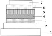
- FIG. 1 is a schematic cross-sectional view showing a structural example of an organic EL element used in the present invention.
- the luminescent material of the present invention is represented by any one of the above general formulas (1) to (21).
- it is a luminescent material represented by any one of the general formulas (2) to (11), more preferably a luminescent material represented by any one of the general formulas (2) to (7). More preferably, it is a luminescent material represented by the general formula (2).
- the organic EL device of the present invention has one or more light-emitting layers between the opposing anode and cathode, and at least one of the light-emitting layers is represented by one of the general formulas (1) to (21). It contains a compound as a luminescent material.
- This organic EL element has a plurality of layers between an anode and a cathode that face each other, and at least one of the plurality of layers is a light emitting layer, and the light emitting layer can contain a host material if necessary.
- General formula (1) will be explained below.
- the compounds represented by the general formulas (1) to (21) typically have a structure in which a benzothiophene skeleton is further fused to an indolocarbazole skeleton fused at a specific position, or a structure similar thereto.
- a 1 is CR 1 , N, or a carbon atom.
- the number of N in A 1 present in one six-membered ring containing A 1 is 2 or less.
- This six-membered ring containing A 1 may be fused with an adjacent ring E, but in that case, two of A 1 are carbon atoms, and these carbon atoms are shared with ring E.
- all A 1 are represented by CR 1 or C.
- R 1 is each independently hydrogen, a cyano group, deuterium, a substituted or unsubstituted diarylamino group having 12 to 44 carbon atoms, a substituted or unsubstituted arylheteroarylamino group having 12 to 44 carbon atoms, a substituted or Unsubstituted diheteroarylamino group having 12 to 44 carbon atoms, aliphatic hydrocarbon group having 1 to 10 carbon atoms, substituted or unsubstituted aromatic hydrocarbon group having 6 to 30 carbon atoms, substituted or unsubstituted carbon It is a substituted or unsubstituted linked aromatic group formed by linking 3 to 30 aromatic heterocyclic groups, or 2 to 5 of the aromatic hydrocarbon group and 2 to 5 of the aromatic heterocyclic groups.
- Diheteroarylamino group having 12 to 24 carbon atoms aliphatic hydrocarbon group having 1 to 8 carbon atoms, substituted or unsubstituted aromatic hydrocarbon group having 6 to 20 carbon atoms, substituted or unsubstituted aromatic hydrocarbon group having 3 to 20 carbon atoms It is an aromatic heterocyclic group, or a substituted or unsubstituted linked aromatic group formed by linking 2 to 4 of the aromatic hydrocarbon group and the aromatic heterocyclic group.
- a substituted or unsubstituted diarylamino group having 12 to 18 carbon atoms preferably, a substituted or unsubstituted diarylamino group having 12 to 18 carbon atoms, a substituted or unsubstituted arylheteroarylamino group having 12 to 18 carbon atoms, an aliphatic hydrocarbon group having 1 to 4 carbon atoms, A substituted or unsubstituted aromatic hydrocarbon group having 6 to 10 carbon atoms, a substituted or unsubstituted aromatic heterocyclic group having 3 to 12 carbon atoms, or the aromatic hydrocarbon group and the aromatic heterocyclic group having 2 , or a substituted or unsubstituted linked aromatic group consisting of three linked aromatic groups.
- At least one R 1 is deuterium, substituted or unsubstituted diarylamino group having 12 to 44 carbon atoms, substituted or unsubstituted arylheteroarylamino group having 12 to 44 carbon atoms, substituted or unsubstituted 12 to 44 carbon atoms 44 diheteroarylamino group, preferably an aliphatic hydrocarbon group having 1 to 10 carbon atoms, at least two R 1 are deuterium, a substituted or unsubstituted diarylamino group having 12 to 44 carbon atoms, a substituted or an unsubstituted arylheteroarylamino group having 12 to 44 carbon atoms, a substituted or unsubstituted diheteroarylamino group having 12 to 44 carbon atoms, and an aliphatic hydrocarbon group having 1 to 10 carbon atoms.
- R 1s are a substituted or unsubstituted diarylamino group having 12 to 44 carbon atoms, a substituted or unsubstituted arylheteroarylamino group having 12 to 44 carbon atoms, or a substituted or unsubstituted arylheteroarylamino group having 12 to 44 carbon atoms.
- R 1s are a substituted or unsubstituted diarylamino group having 12 to 44 carbon atoms, a substituted or unsubstituted arylheteroarylamino group having 12 to 44 carbon atoms, or a substituted or unsubstituted arylheteroarylamino group having 12 to 44 carbon atoms.
- ⁇ 44 diheteroarylamino group an aliphatic hydrocarbon group having 1 to 10 carbon atoms.
- R 1 represents an unsubstituted diarylamino group, an unsubstituted arylheteroarylamino group, an unsubstituted diheteroarylamino group, or an aliphatic hydrocarbon group
- diphenylamino dibiphenylamino, Phenylbiphenylamino, naphthylphenylamino, dinaphthylamino, dianthranylamino, diphenanthrenylamino, dibenzofuranylphenylamino, dibenzofuranylbiphenylamino, bisdibenzofuranylamino, methyl, ethyl, propyl, butyl, pentyl , hexyl, heptyl, octyl, nonyl, and decyl.
- R 1 is an unsubstituted aromatic hydrocarbon group, aromatic heterocyclic group, or linked aromatic group
- benzene naphthalene, acenaphthene, acenaphthylene, azulene, anthracene, chrysene, pyrene, phenanthrene, Triphenylene, fluorene, benzo[a]anthracene, pyridine, pyrimidine, triazine, thiophene, isothiazole, thiazole, pyridazine, pyrrole, pyrazole, imidazole, triazole, thiadiazole, pyrazine, furan, isoxazole, quinoline, isoquinoline, quinoxaline, quinazoline, thiadiazole , phthalazine, tetrazole, indole, benzofuran, benzothiophene, benzoxazole, benzothi
- benzene, naphthalene, azulene, pyridine, pyrimidine, triazine, thiophene, isothiazole, thiazole, pyridazine, pyrrole, pyrazole, imidazole, triazole, thiadiazole, pyrazine, furan, isoxazole, quinoline, isoquinoline, quinoxaline, quinazoline, thiadiazole , phthalazine, tetrazole, indole, benzofuran, benzothiophene, benzoxazole, benzothiazole, indazole, benzimidazole, benzotriazole, benzisothiazole, benzothiadiazole, purine, pyranone, coumarin, isocoumarin, chromone, dibenzofuran, dibenzothiophene, dibenzoseleno Examples include groups formed by removing one hydrogen
- aromatic hydrocarbon group aromatic heterocyclic group, or linked aromatic group may each have a substituent.
- aryl group and heteroaryl group contained in the diarylamino group, arylheteroarylamino group, and diheteroarylamino group may be substituted by the same applies.
- the substituents when having a substituent include a cyano group, an aliphatic hydrocarbon group having 1 to 10 carbon atoms, a diarylamino group having 12 to 30 carbon atoms, an arylheteroarylamino group having 12 to 30 carbon atoms, and a 12-carbon atom group.
- a cyano group an aliphatic hydrocarbon group having 1 to 10 carbon atoms
- a diarylamino group having 12 to 30 carbon atoms an arylheteroarylamino group having 12 to 30 carbon atoms
- a 12-carbon atom group -30 diheteroarylamino groups, alkoxy groups having 1 to 10 carbon atoms, aryloxy groups having 6 to 18 carbon atoms, alkylthio groups having 1 to 10 carbon atoms, and arylthio groups having 6 to 18 carbon atoms.
- the substituent when the substituent is an aliphatic hydrocarbon group having 1 to 10 carbon atoms, it may be linear,
- diarylamino group, arylheteroarylamino group, diheteroarylamino group, aryloxy group, and arylthio group are the aromatic hydrocarbon group, aromatic heterocyclic group, aromatic ring of the linked aromatic group, Alternatively, when substituting an aryl group or a heteroaryl group contained in a diarylamino group, arylheteroarylamino group, or diheteroarylamino group, nitrogen and carbon, oxygen and carbon, or sulfur and carbon are bonded together with a single bond.
- the number of substituents is 0 to 5, preferably 0 to 2.
- the number of carbon atoms in the substituent is not included in the calculation of the number of carbon atoms. However, it is preferable that the total number of carbon atoms including the number of carbon atoms of the substituents satisfies the above range.
- substituents include cyano, methyl, ethyl, propyl, butyl, pentyl, hexyl, heptyl, octyl, nonyl, decyl, diphenylamino, naphthylphenylamino, dinaphthylamino, dianthranylamino, diphenane.
- Threnylamino dibenzofuranylphenylamino, dibenzofuranylbiphenylamino, bisdibenzofuranylamino, methoxy, ethoxy, phenol, diphenyloxy, methylthio, ethylthio, thiophenol, or diphenylthio.
- cyano methyl, ethyl, propyl, butyl, pentyl, hexyl, heptyl, octyl, diphenylamino, naphthylphenylamino, dinaphthylamino, dibenzofuranylphenylamino, dibenzofuranylbiphenylamino, bisdibenzofuranylamino , phenol, or thiophenol.
- a linked aromatic group refers to an aromatic group in which aromatic groups are linked by bonding with a single bond. It is an aromatic group in which two or more aromatic groups are connected, and these may be linear or branched.
- the aromatic group may be an aromatic hydrocarbon group or an aromatic heterocyclic group, and the plurality of aromatic groups may be the same or different.
- An aromatic group corresponding to a linked aromatic group is different from a substituted aromatic group.
- hydrogen may also be deuterium. That is, in general formulas (1) to (21), some or all of the H's in R 1 or its substituents may be deuterium.
- Each ring E is independently a heterocycle represented by formula (1a), and ring E is fused with an adjacent ring at any position.
- a, b, c, and d each independently represent 0 or 1, and a, b, c, and d are never all 0.
- Preferred embodiments of the general formula (1) include the general formulas (2) to (11). More preferred are the general formulas (2) to (7), and even more preferred is the general formula (2).
- General formulas (2) to (7) correspond to structures in which a, b and c are all 0 and d is 1 in general formula (1), and general formulas (8) to (11) correspond to a, It corresponds to a structure where both c and d are 0 and b is 1. Also, in general formulas (12) to (17), a and d are both 1, and b and c are both 0, and in general formulas (18) to (21), a and d are both 0. corresponds to a structure in which both b and c are 1.
- luminescent materials represented by general formulas (1) to (21) are shown below, but the invention is not limited to these exemplified compounds.
- an organic EL element that emits light with high efficiency and has high driving stability and is excellent in practical use. Can be done.
- FIG. 1 is a cross-sectional view showing an example of the structure of a general organic EL device used in the present invention, in which 1 is a substrate, 2 is an anode, 3 is a hole injection layer, 4 is a hole transport layer, and 5 is a light emitting layer. , 6 represents an electron transport layer, and 7 represents a cathode.
- the organic EL device of the present invention may have an exciton blocking layer adjacent to the light emitting layer, or may have an electron blocking layer between the light emitting layer and the hole injection layer.
- the exciton blocking layer can be inserted into either the cathode side or the anode side of the light emitting layer, or can be inserted into both at the same time.
- the organic EL device of the present invention has an anode, a light emitting layer, and a cathode as essential layers, but in addition to the essential layers, it may also have a hole injection transport layer and an electron injection transport layer, and further includes a light emitting layer and an electron injection transport layer. It is preferable to have a hole blocking layer between the transport layers.
- the hole injection transport layer means either or both of the hole injection layer and the hole transport layer
- the electron injection transport layer means either or both of the electron injection layer and the electron transport layer.
- the layers constituting the laminated structure on the substrate other than the electrodes such as the anode and the cathode may be collectively referred to as organic layers.
- the organic EL element of the present invention is preferably supported by a substrate.
- a substrate There are no particular restrictions on this substrate, and any substrate that has been conventionally used in organic EL devices may be used, such as glass, transparent plastic, quartz, or the like.
- anode material in an organic EL element a material consisting of a metal, an alloy, an electrically conductive compound, or a mixture thereof having a large work function (4 eV or more) is preferably used.
- electrode materials include metals such as Au, conductive transparent materials such as CuI, indium tin oxide (ITO), SnO2, and ZnO.
- an amorphous material such as IDIXO (In2O3-ZnO) that can be used to form a transparent conductive film may also be used.
- these electrode materials may be formed into a thin film by methods such as vapor deposition or sputtering, and a pattern of the desired shape may be formed by photolithography, or if high pattern precision is not required (approximately 100 ⁇ m or more).
- a pattern may be formed through a mask having a desired shape during vapor deposition or sputtering of the electrode material.
- a coatable substance such as an organic conductive compound
- a wet film forming method such as a printing method or a coating method may be used.
- the transmittance be greater than 10%, and the sheet resistance of the anode is preferably several hundred ⁇ / ⁇ or less.
- the film thickness depends on the material, it is usually selected in the range of 10 to 1000 nm, preferably 10 to 200 nm.
- the cathode material a material consisting of a metal with a small work function (4 eV or less) (referred to as an electron-injecting metal), an alloy, an electrically conductive compound, or a mixture thereof is used.
- an electron-injecting metal a material consisting of a metal with a small work function (4 eV or less) (referred to as an electron-injecting metal), an alloy, an electrically conductive compound, or a mixture thereof.
- electrode materials include sodium, sodium-potassium alloy, magnesium, lithium, magnesium/copper mixture, magnesium/silver mixture, magnesium/aluminum mixture, magnesium/indium mixture, aluminum/aluminum oxide (Al2O3) mixture. , indium, lithium/aluminum mixtures, rare earth metals, and the like.
- mixtures of electron injection metals and second metals that are stable metals with larger work function values such as magnesium/silver mixtures, magnesium /aluminum mixtures, magnesium/indium mixtures, aluminum/aluminum oxide (Al2O3) mixtures, lithium/aluminum mixtures, aluminum, etc. are suitable.
- the cathode can be manufactured by forming a thin film of these cathode materials by a method such as vapor deposition or sputtering.
- the sheet resistance of the cathode is preferably several hundred ⁇ / ⁇ or less, and the film thickness is usually selected in the range of 10 nm to 5 ⁇ m, preferably 50 to 200 nm. Note that, in order to transmit the emitted light, it is advantageous if either the anode or the cathode of the organic EL element is transparent or semi-transparent, as this improves the luminance of the emitted light.
- a transparent or translucent cathode can be produced. By applying this, it is possible to fabricate an element in which both the anode and cathode are transparent.
- the light-emitting layer is a layer that emits light after excitons are generated by recombination of holes and electrons injected from the anode and cathode, respectively.
- the light-emitting materials represented by the general formulas (1) to (21) may be used alone, or this light-emitting material may be used together with a host material.
- the luminescent material is responsible for emitting light in the device.
- the content of the luminescent material is preferably 0.1 to 50 wt%, more preferably 0.1 to 40 wt%, based on the host material.
- the host material in the light emitting layer known host materials used in phosphorescent light emitting devices and fluorescent light emitting devices can be used.
- Known host materials that can be used include compounds that have hole-transporting ability, electron-transporting ability, and a high glass transition temperature, and have a triplet excitation energy (T1 ) It is preferable that the triplet excitation energy (T1) is larger than the triplet excitation energy (T1).
- host materials are known from numerous patent documents and can be selected from them.
- Specific examples of host materials include, but are not limited to, indole compounds, carbazole compounds and multimers thereof, anthracene compounds, indolocarbazole compounds, pyridine compounds, pyrimidine compounds, triazine compounds, triazole compounds, oxazole compounds, Oxadiazole compounds, imidazole compounds, phenylenediamine compounds, arylamine compounds, anthracene compounds, fluorenone compounds, stilbene compounds, triphenylene compounds, carborane compounds, porphyrin compounds, phthalocyanine compounds, metal complexes of 8-quinolinol compounds, metal phthalocyanines, benzoxazole and various metal complexes represented by metal complexes of benzothiazole compounds, polymers such as poly(N-vinylcarbazole) compounds, aniline copolymer compounds, thiophene oligomers, polythiophene compounds, polyphenylene compounds,
- Examples include compounds.
- Preferred examples include carbazole compounds and multimers thereof, anthracene compounds, indolocarbazole compounds, pyridine compounds, pyrimidine compounds, triazine compounds, anthracene compounds, triphenylene compounds, carborane compounds, and porphyrin compounds. More preferred are biscarbazole compounds, tricarbazole compounds, or anthracene compounds, which are multimers of carbazole compounds. Note that hydrogen in the host material typified by the above compounds may be replaced with deuterium.
- anthracene compounds are shown below, but the invention is not limited to these exemplified compounds.
- Only one type of host may be used in one light emitting layer, or two or more types of hosts may be used.
- at least one type is preferably an electron-transporting compound such as the biscarbazole compound, tricarbazole compound, or anthracene compound described above, and the other hosts are carbazole compounds.
- a hole-transporting compound such as an indolocarbazole compound is preferable.
- each host can be deposited from a different deposition source, or multiple types of hosts can be deposited simultaneously from one deposition source by premixing them to form a premix before deposition. .
- the luminescent material and the host material can be deposited from different deposition sources, or the luminescent material and the host material can be deposited simultaneously from one deposition source by premixing them to form a premix before deposition.
- premixing method that allows for as uniform a mixture as possible, such as pulverization, heating and melting under reduced pressure or an inert gas atmosphere such as nitrogen, and sublimation.
- the method is not limited.
- the host and its premix may be in the form of powder, stick, or granule.
- An injection layer is a layer provided between an electrode and an organic layer in order to reduce driving voltage and improve luminance.There are a hole injection layer and an electron injection layer. It may also be present between the cathode and the light emitting layer or electron transport layer. An injection layer can be provided as necessary.
- the hole-blocking layer has the function of an electron-transporting layer, and is made of a hole-blocking material that has the function of transporting electrons but has an extremely low ability to transport holes. By preventing this, the probability of recombination of electrons and holes in the light emitting layer can be improved.
- the hole blocking layer can be made of a known hole blocking material. Further, a plurality of hole blocking materials may be used in combination.
- an electron blocking layer has the function of a hole transport layer, and by transporting holes and blocking electrons, it can improve the probability that electrons and holes will recombine in the light-emitting layer.
- known electron blocking layer materials can be used as the material for the electron blocking layer.
- the exciton blocking layer is a layer that prevents excitons generated by the recombination of holes and electrons in the light emitting layer from diffusing into the charge transport layer. It becomes possible to efficiently confine the light within the light emitting layer, and the light emitting efficiency of the device can be improved.
- the exciton blocking layer can be inserted between two adjacent light-emitting layers in a device in which two or more light-emitting layers are adjacent. As a material for such an exciton blocking layer, a known exciton blocking layer material can be used.
- Layers adjacent to the light-emitting layer include a hole-blocking layer, an electron-blocking layer, and an exciton-blocking layer, but if these layers are not provided, the adjacent layers will be a hole-transporting layer, an electron-transporting layer, etc.
- the hole transport layer is made of a hole transport material having a function of transporting holes, and the hole transport layer may be provided as a single layer or multiple layers.
- the hole transport material has either hole injection or transport or electron barrier properties, and may be either organic or inorganic.
- any compound selected from conventionally known compounds can be used. Examples of such hole transport materials include porphyrin derivatives, arylamine derivatives, triazole derivatives, oxadiazole derivatives, imidazole derivatives, polyarylalkane derivatives, phenylenediamine derivatives, arylamine derivatives, amino-substituted chalcone derivatives, oxazole derivatives, and styrylanthracene.
- the electron transport layer is made of a material that has a function of transporting electrons, and the electron transport layer can be provided in a single layer or in multiple layers.
- the electron transport material (which may also serve as a hole blocking material) may have the function of transmitting electrons injected from the cathode to the light emitting layer.
- any compound selected from conventionally known compounds can be used, such as polycyclic aromatic derivatives such as naphthalene, anthracene, and phenanthroline, and tris(8-quinolinolato)aluminum(III).
- the method for forming each layer is not particularly limited, and may be produced by either a dry process or a wet process.
- Example 1 A thin film shown below was formed on a quartz substrate by vacuum evaporation at a vacuum degree of 4.0 ⁇ 10 ⁇ 5 Pa.
- Compound (H23) as a host and compound (D1) as a dopant were co-deposited from different deposition sources to form a light-emitting layer having a thickness of 100 nm.
- codeposition was carried out under vapor deposition conditions such that the concentration of compound (D1) was 1% by mass.
- An organic thin film according to Example 1 was produced.
- Photoluminescence quantum yield (PLQY) measurement was performed on the above organic thin film using Absolute PL Quantum Yield Measurement C9920-03G system (Hamamatsu Photonics Co., Ltd.).
- C9920-03G system Absolute PL Quantum Yield Measurement C9920-03G system
- maximum emission wavelength, half-width, PLQY and CIE coordinates are determined using software U6039-05 version 3.6.0.
- the maximum emission wavelength and half-value width are given in nm
- PLQY is given in %
- CIE coordinates are given as x and y values. Note that the excitation wavelength in the PLQY measurement was 340 nm.
- ⁇ EST is calculated by subtracting T1 from S1 calculated above.
- Comparative example 1 An organic thin film was produced in the same manner as in Example 1, except that BD-1 was used as the dopant, and the maximum emission wavelength, half-width, PLQY, CIE coordinates, and ⁇ EST were determined in the same manner as in Example 1.
- Table 1 shows the results of measuring the maximum emission wavelength, half-value width, chromaticity (CIEx, CIEy), PLQY, and ⁇ EST of the emission spectrum of the produced organic thin film.
- Table 1 shows that the luminescent material of the present invention exhibits a PLQY equivalent to that of the organic thin film of Comparative Example 1 using BD-1 as a luminescent material, and has highly efficient characteristics. It turns out that.
- S1 and T1 can be determined by actual measurement as described above, or can be determined by theoretical calculation using a molecular orbital method program as shown below.
- ⁇ EST(theo) obtained by the following calculation method has a high correlation with the actually measured ⁇ EST, and in general, the smaller the value, the more likely reverse intersystem crossing will occur and the triplet excitons will be efficiently used for light emission. Therefore, high luminous efficiency can be expected.
- thermally activated delayed fluorescent materials with a small ⁇ EST(theo) generally have a small actually measured ⁇ EST.
- Structural optimization calculations are performed at the B3LYP/6-31G* level using density half-function theory (DFT) using the molecular orbital method program Gaussian 16 for D1, D13, and D23, which are luminescent materials represented by general formula (1). was performed, and S1(theo), T1(theo), and ⁇ EST(theo) were calculated at the TD-B3LYP/6-31G* level. The results are shown in Table 2.
- DFT density half-function theory
- Example 2 On a glass substrate on which an anode made of ITO with a film thickness of 70 nm was formed, the following thin films were laminated by vacuum evaporation at a degree of vacuum of 4.0 ⁇ 10 ⁇ 5 Pa.
- HAT-CN shown above was formed as a hole injection layer to a thickness of 10 nm on ITO, and then HT-1 was formed as a hole transport layer to a thickness of 25 nm.
- HT-2 was formed to a thickness of 5 nm as an electron blocking layer.
- Compound (H31) as a host and compound (D1) as a dopant were co-deposited from different deposition sources to form a light-emitting layer having a thickness of 30 nm.
- codeposition was carried out under vapor deposition conditions such that the concentration of compound (D1) was 1% by mass.
- compound (H31) was formed to a thickness of 5 nm as a hole blocking layer.
- ALQ3 was formed to a thickness of 40 nm as an electron transport layer.
- lithium fluoride (LiF) was formed to a thickness of 1 nm as an electron injection layer on the electron transport layer.
- aluminum (Al) was formed to a thickness of 70 nm as a cathode on the electron injection layer, thereby producing an organic EL device according to Example 2.
- Comparative example 2 An organic EL device was produced in the same manner as in Example 2 except that BD-1 was used as the dopant.
- Table 3 shows the maximum emission wavelength, external quantum efficiency, and lifetime of the emission spectrum of the produced organic EL device.
- the maximum emission wavelength and external quantum efficiency are the values when the driving current density is 2.5 mA/cm 2 and are initial characteristics.
- the lifespan was measured by measuring the time until the brightness attenuated to 90% of the initial brightness when the driving current density was 40 mA/cm 2 .
- Table 3 shows that the organic EL device using the luminescent material of the present invention emits blue light from the maximum emission wavelength, and compared with the organic EL device using BD-1 as the luminescent material, the life characteristics are Particularly excellent results were shown.
- the luminescent material of the present invention it is possible to obtain a practically useful organic EL element that emits light with high efficiency and has high driving stability. Furthermore, the luminescent material of the present invention exhibits a maximum wavelength in the blue, light blue, or green spectral region. This luminescent material exhibits a maximum wavelength particularly between 410 nm and 550 nm, preferably between 430 nm and 495 nm.
- the photoluminescence quantum yield of the luminescent material of the present invention can be 40% or more. Use of the luminescent materials of the present invention results in more efficient devices. Moreover, an organic EL element having a light emitting layer containing this has high luminous efficiency.
Landscapes
- Chemical & Material Sciences (AREA)
- Engineering & Computer Science (AREA)
- Materials Engineering (AREA)
- Physics & Mathematics (AREA)
- Spectroscopy & Molecular Physics (AREA)
- Optics & Photonics (AREA)
- Organic Chemistry (AREA)
- Inorganic Chemistry (AREA)
- Electroluminescent Light Sources (AREA)
Priority Applications (4)
| Application Number | Priority Date | Filing Date | Title |
|---|---|---|---|
| KR1020257008818A KR20250068642A (ko) | 2022-09-13 | 2023-09-11 | 발광 재료 및 유기 전계 발광 소자 |
| JP2024546964A JPWO2024058146A1 (https=) | 2022-09-13 | 2023-09-11 | |
| US19/108,055 US20260082760A1 (en) | 2022-09-13 | 2023-09-11 | Luminescent material, and organic electroluminescent element |
| CN202380060915.9A CN119744578A (zh) | 2022-09-13 | 2023-09-11 | 发光材料及有机电场发光元件 |
Applications Claiming Priority (2)
| Application Number | Priority Date | Filing Date | Title |
|---|---|---|---|
| JP2022145289 | 2022-09-13 | ||
| JP2022-145289 | 2022-09-13 |
Publications (1)
| Publication Number | Publication Date |
|---|---|
| WO2024058146A1 true WO2024058146A1 (ja) | 2024-03-21 |
Family
ID=90275056
Family Applications (1)
| Application Number | Title | Priority Date | Filing Date |
|---|---|---|---|
| PCT/JP2023/033101 Ceased WO2024058146A1 (ja) | 2022-09-13 | 2023-09-11 | 発光材料、及び有機電界発光素子 |
Country Status (5)
| Country | Link |
|---|---|
| US (1) | US20260082760A1 (https=) |
| JP (1) | JPWO2024058146A1 (https=) |
| KR (1) | KR20250068642A (https=) |
| CN (1) | CN119744578A (https=) |
| WO (1) | WO2024058146A1 (https=) |
Cited By (1)
| Publication number | Priority date | Publication date | Assignee | Title |
|---|---|---|---|---|
| US20230322802A1 (en) * | 2022-04-08 | 2023-10-12 | Samsung Display Co., Ltd. | Light emitting device and fused polycyclic compound for the light emitting device |
Citations (2)
| Publication number | Priority date | Publication date | Assignee | Title |
|---|---|---|---|---|
| JP2021506866A (ja) * | 2017-12-19 | 2021-02-22 | メルク、パテント、ゲゼルシャフト、ミット、ベシュレンクテル、ハフツングMerck Patent GmbH | 複素環式化合物 |
| JP2021172592A (ja) * | 2020-04-20 | 2021-11-01 | 出光興産株式会社 | 化合物及び有機エレクトロルミネッセンス素子 |
Family Cites Families (4)
| Publication number | Priority date | Publication date | Assignee | Title |
|---|---|---|---|---|
| US20100295444A1 (en) | 2009-05-22 | 2010-11-25 | Idemitsu Kosan Co., Ltd. | Organic electroluminescence device |
| JP5124785B2 (ja) | 2009-12-07 | 2013-01-23 | 新日鉄住金化学株式会社 | 有機発光材料及び有機発光素子 |
| WO2019111971A1 (ja) | 2017-12-06 | 2019-06-13 | 出光興産株式会社 | 有機エレクトロルミネッセンス素子及び新規化合物 |
| WO2021167045A1 (ja) | 2020-02-21 | 2021-08-26 | 出光興産株式会社 | 化合物及び有機エレクトロルミネッセンス素子 |
-
2023
- 2023-09-11 WO PCT/JP2023/033101 patent/WO2024058146A1/ja not_active Ceased
- 2023-09-11 KR KR1020257008818A patent/KR20250068642A/ko active Pending
- 2023-09-11 CN CN202380060915.9A patent/CN119744578A/zh active Pending
- 2023-09-11 US US19/108,055 patent/US20260082760A1/en active Pending
- 2023-09-11 JP JP2024546964A patent/JPWO2024058146A1/ja active Pending
Patent Citations (2)
| Publication number | Priority date | Publication date | Assignee | Title |
|---|---|---|---|---|
| JP2021506866A (ja) * | 2017-12-19 | 2021-02-22 | メルク、パテント、ゲゼルシャフト、ミット、ベシュレンクテル、ハフツングMerck Patent GmbH | 複素環式化合物 |
| JP2021172592A (ja) * | 2020-04-20 | 2021-11-01 | 出光興産株式会社 | 化合物及び有機エレクトロルミネッセンス素子 |
Cited By (1)
| Publication number | Priority date | Publication date | Assignee | Title |
|---|---|---|---|---|
| US20230322802A1 (en) * | 2022-04-08 | 2023-10-12 | Samsung Display Co., Ltd. | Light emitting device and fused polycyclic compound for the light emitting device |
Also Published As
| Publication number | Publication date |
|---|---|
| JPWO2024058146A1 (https=) | 2024-03-21 |
| KR20250068642A (ko) | 2025-05-16 |
| CN119744578A (zh) | 2025-04-01 |
| US20260082760A1 (en) | 2026-03-19 |
Similar Documents
| Publication | Publication Date | Title |
|---|---|---|
| JP7456997B2 (ja) | 有機電界発光素子用溶融混合物、及び有機電界発光素子 | |
| JP7037543B2 (ja) | 有機電界発光素子 | |
| EP4083033B1 (en) | Organic electroluminescent element | |
| KR102659607B1 (ko) | 유기 전계 발광 소자 | |
| JP7332577B2 (ja) | 有機電界発光素子 | |
| JP2025157550A (ja) | 有機電界発光素子 | |
| WO2022009883A1 (ja) | 熱活性化遅延蛍光材料、及び有機電界発光素子 | |
| KR20240152348A (ko) | 유기 전계 발광 소자용 재료 및 유기 전계 발광 소자 | |
| WO2024058146A1 (ja) | 発光材料、及び有機電界発光素子 | |
| JP7094215B2 (ja) | 熱活性化遅延蛍光発光材料、及び有機電界発光素子 | |
| WO2025041677A1 (ja) | 有機電界発光素子用混合材料及び有機電界発光素子 | |
| JP7801712B2 (ja) | 発光材料、及び有機電界発光素子 | |
| WO2024135277A1 (ja) | 有機電界発光素子 | |
| EP4322236A1 (en) | Light-emitting material, and organic electroluminescent element | |
| KR20250121590A (ko) | 화합물 및 유기 전계 발광 소자용 재료 그리고 유기 전계 발광 소자 | |
| JP7742829B2 (ja) | 有機電界発光素子 | |
| JP7847585B2 (ja) | 有機電界発光素子用材料、及び有機電界発光素子 | |
| WO2023157629A1 (ja) | 発光材料、及び有機電界発光素子 | |
| WO2025182720A1 (ja) | 有機電界発光素子用混合材料及び有機電界発光素子 | |
| WO2025105314A1 (ja) | 有機電界発光素子用混合材料及び有機電界発光素子 | |
| WO2025169870A1 (ja) | 有機電界発光素子用混合材料及び有機電界発光素子 | |
| WO2026014373A1 (ja) | 有機電界発光素子用ホスト材料及びこれを用いた有機電界発光素子 | |
| KR20260055415A (ko) | 유기 전계 발광 소자용 혼합 재료 및 유기 전계 발광 소자 |
Legal Events
| Date | Code | Title | Description |
|---|---|---|---|
| 121 | Ep: the epo has been informed by wipo that ep was designated in this application |
Ref document number: 23865499 Country of ref document: EP Kind code of ref document: A1 |
|
| DPE1 | Request for preliminary examination filed after expiration of 19th month from priority date (pct application filed from 20040101) | ||
| WWE | Wipo information: entry into national phase |
Ref document number: 2024546964 Country of ref document: JP |
|
| WWE | Wipo information: entry into national phase |
Ref document number: 202380060915.9 Country of ref document: CN |
|
| ENP | Entry into the national phase |
Ref document number: 20257008818 Country of ref document: KR Kind code of ref document: A |
|
| WWP | Wipo information: published in national office |
Ref document number: 202380060915.9 Country of ref document: CN |
|
| NENP | Non-entry into the national phase |
Ref country code: DE |
|
| 122 | Ep: pct application non-entry in european phase |
Ref document number: 23865499 Country of ref document: EP Kind code of ref document: A1 |