WO2024057838A1 - 半導体装置 - Google Patents
半導体装置 Download PDFInfo
- Publication number
- WO2024057838A1 WO2024057838A1 PCT/JP2023/030130 JP2023030130W WO2024057838A1 WO 2024057838 A1 WO2024057838 A1 WO 2024057838A1 JP 2023030130 W JP2023030130 W JP 2023030130W WO 2024057838 A1 WO2024057838 A1 WO 2024057838A1
- Authority
- WO
- WIPO (PCT)
- Prior art keywords
- lead
- thickness direction
- semiconductor device
- die pad
- resin
- Prior art date
- Legal status (The legal status is an assumption and is not a legal conclusion. Google has not performed a legal analysis and makes no representation as to the accuracy of the status listed.)
- Ceased
Links
Images


















Classifications
-
- H—ELECTRICITY
- H10—SEMICONDUCTOR DEVICES; ELECTRIC SOLID-STATE DEVICES NOT OTHERWISE PROVIDED FOR
- H10W—GENERIC PACKAGES, INTERCONNECTIONS, CONNECTORS OR OTHER CONSTRUCTIONAL DETAILS OF DEVICES COVERED BY CLASS H10
- H10W70/00—Package substrates; Interposers; Redistribution layers [RDL]
- H10W70/40—Leadframes
- H10W70/411—Chip-supporting parts, e.g. die pads
- H10W70/417—Bonding materials between chips and die pads
-
- H—ELECTRICITY
- H10—SEMICONDUCTOR DEVICES; ELECTRIC SOLID-STATE DEVICES NOT OTHERWISE PROVIDED FOR
- H10W—GENERIC PACKAGES, INTERCONNECTIONS, CONNECTORS OR OTHER CONSTRUCTIONAL DETAILS OF DEVICES COVERED BY CLASS H10
- H10W70/00—Package substrates; Interposers; Redistribution layers [RDL]
- H10W70/40—Leadframes
- H10W70/421—Shapes or dispositions
- H10W70/424—Cross-sectional shapes
- H10W70/427—Bent parts
- H10W70/429—Bent parts being the outer leads
-
- H—ELECTRICITY
- H10—SEMICONDUCTOR DEVICES; ELECTRIC SOLID-STATE DEVICES NOT OTHERWISE PROVIDED FOR
- H10W—GENERIC PACKAGES, INTERCONNECTIONS, CONNECTORS OR OTHER CONSTRUCTIONAL DETAILS OF DEVICES COVERED BY CLASS H10
- H10W72/00—Interconnections or connectors in packages
-
- H—ELECTRICITY
- H10—SEMICONDUCTOR DEVICES; ELECTRIC SOLID-STATE DEVICES NOT OTHERWISE PROVIDED FOR
- H10W—GENERIC PACKAGES, INTERCONNECTIONS, CONNECTORS OR OTHER CONSTRUCTIONAL DETAILS OF DEVICES COVERED BY CLASS H10
- H10W74/00—Encapsulations, e.g. protective coatings
-
- H—ELECTRICITY
- H10—SEMICONDUCTOR DEVICES; ELECTRIC SOLID-STATE DEVICES NOT OTHERWISE PROVIDED FOR
- H10W—GENERIC PACKAGES, INTERCONNECTIONS, CONNECTORS OR OTHER CONSTRUCTIONAL DETAILS OF DEVICES COVERED BY CLASS H10
- H10W74/00—Encapsulations, e.g. protective coatings
- H10W74/10—Encapsulations, e.g. protective coatings characterised by their shape or disposition
- H10W74/111—Encapsulations, e.g. protective coatings characterised by their shape or disposition the semiconductor body being completely enclosed
-
- H—ELECTRICITY
- H10—SEMICONDUCTOR DEVICES; ELECTRIC SOLID-STATE DEVICES NOT OTHERWISE PROVIDED FOR
- H10W—GENERIC PACKAGES, INTERCONNECTIONS, CONNECTORS OR OTHER CONSTRUCTIONAL DETAILS OF DEVICES COVERED BY CLASS H10
- H10W72/00—Interconnections or connectors in packages
- H10W72/50—Bond wires
- H10W72/531—Shapes of wire connectors
- H10W72/533—Cross-sectional shape
- H10W72/534—Cross-sectional shape being rectangular
-
- H—ELECTRICITY
- H10—SEMICONDUCTOR DEVICES; ELECTRIC SOLID-STATE DEVICES NOT OTHERWISE PROVIDED FOR
- H10W—GENERIC PACKAGES, INTERCONNECTIONS, CONNECTORS OR OTHER CONSTRUCTIONAL DETAILS OF DEVICES COVERED BY CLASS H10
- H10W90/00—Package configurations
-
- H—ELECTRICITY
- H10—SEMICONDUCTOR DEVICES; ELECTRIC SOLID-STATE DEVICES NOT OTHERWISE PROVIDED FOR
- H10W—GENERIC PACKAGES, INTERCONNECTIONS, CONNECTORS OR OTHER CONSTRUCTIONAL DETAILS OF DEVICES COVERED BY CLASS H10
- H10W90/00—Package configurations
- H10W90/701—Package configurations characterised by the relative positions of pads or connectors relative to package parts
- H10W90/751—Package configurations characterised by the relative positions of pads or connectors relative to package parts of bond wires
- H10W90/756—Package configurations characterised by the relative positions of pads or connectors relative to package parts of bond wires between a chip and a stacked lead frame, conducting package substrate or heat sink
Definitions
- the present disclosure relates to a semiconductor device.
- Patent Document 1 discloses a semiconductor device including a first lead, a third lead, a semiconductor element, a bonding wire, and a sealing resin.
- the semiconductor element is mounted on the mounting portion of the third lead and connected to the first lead by a bonding wire.
- the sealing resin covers a portion of each lead, the semiconductor element, and the bonding wire.
- the mounting part main surface on which the semiconductor element of the mounting part is mounted and the wire bonding main surface of the first lead to which the bonding wire is bonded are at the same position in the z direction (thickness direction). It is.
- semiconductor devices are required to be thinner. In the above semiconductor device, when the semiconductor element is made thinner and the thickness of the sealing resin is further reduced, the bonding wire may come into contact with the mounting portion due to the lowering of the bonding wire loop.
- An object of the present disclosure is to provide a semiconductor device that is improved over the conventional semiconductor device. Particularly, in view of the above-described circumstances, one object of the present disclosure is to provide a semiconductor device that can suppress contact of a wire (bonding wire) with a die pad portion (mounting portion).
- a semiconductor device provided by one aspect of the present disclosure includes a semiconductor element, a first lead main surface facing the first side in the thickness direction and on which the semiconductor element is mounted, and a first lead main surface facing the second side in the thickness direction.
- a first lead including a die pad portion having a first lead back surface facing toward the front side, and a first lead side surface facing a first side in a first direction perpendicular to the thickness direction;
- the semiconductor device includes a second lead spaced apart from the side, and a wire electrically connected to the semiconductor element and the second lead.
- the die pad portion further includes a contact avoidance surface connected to the first lead main surface and the first lead side surface. The contact avoidance surface overlaps the wire when viewed in the thickness direction, and is located on a second side in the thickness direction from the first lead main surface in the thickness direction.
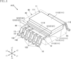
- FIG. 1 is a perspective view showing a semiconductor device according to a first embodiment of the present disclosure.
- FIG. 2 is a perspective view showing a semiconductor device according to the first embodiment of the present disclosure.
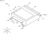
- FIG. 3 is a perspective view showing a semiconductor device according to the first embodiment of the present disclosure.
- FIG. 4 is a perspective view of essential parts of a semiconductor device according to a first embodiment of the present disclosure.
- FIG. 5 is a perspective view of a main part of a semiconductor device according to a first embodiment of the present disclosure.
- FIG. 6 is a plan view showing a semiconductor device according to the first embodiment of the present disclosure.
- FIG. 7 is a bottom view showing the semiconductor device according to the first embodiment of the present disclosure.
- FIG. 1 is a perspective view showing a semiconductor device according to a first embodiment of the present disclosure.
- FIG. 2 is a perspective view showing a semiconductor device according to the first embodiment of the present disclosure.
- FIG. 3 is a perspective view showing a semiconductor device according to the first embodiment
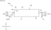
- FIG. 8 is a front view showing the semiconductor device according to the first embodiment of the present disclosure.
- FIG. 9 is a side view showing the semiconductor device according to the first embodiment of the present disclosure.
- FIG. 10 is a plan view of main parts showing a semiconductor device according to a first embodiment of the present disclosure.
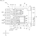
- FIG. 11 is a bottom view of essential parts showing the semiconductor device according to the first embodiment of the present disclosure.
- FIG. 12 is a sectional view taken along line XII-XII in FIG. 11.
- FIG. 13 is an enlarged view of FIG. 12.
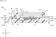
- FIG. 14 is a sectional view taken along line XIV-XIV in FIG. 11.
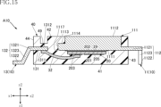
- FIG. 15 is a sectional view taken along line XV-XV in FIG. 11.
- FIG. 11 is a sectional view taken along line XV-XV in FIG. 11.
- FIG. 16 is a cross-sectional view taken along line XVI-XVI in FIG. 11.
- FIG. 17 is a cross-sectional view showing how the semiconductor device according to the first embodiment of the present disclosure is used.
- FIG. 18 is an enlarged cross-sectional view showing a first modification of the semiconductor device according to the first embodiment of the present disclosure.
- FIG. 19 is an enlarged cross-sectional view showing a second modification of the semiconductor device according to the first embodiment of the present disclosure.
- FIG. 20 is an enlarged cross-sectional view showing a third modification of the semiconductor device according to the first embodiment of the present disclosure.
- FIG. 21 is an enlarged cross-sectional view showing a fourth modification of the semiconductor device according to the first embodiment of the present disclosure.
- FIG. 18 is an enlarged cross-sectional view showing a first modification of the semiconductor device according to the first embodiment of the present disclosure.
- FIG. 19 is an enlarged cross-sectional view showing a second modification of the semiconductor device according to the first embodiment of the present disclosure.
- FIG. 22 is an enlarged cross-sectional view showing a fifth modification of the semiconductor device according to the first embodiment of the present disclosure.
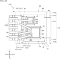
- FIG. 23 is a bottom view of essential parts showing a sixth modification example of the semiconductor device according to the first embodiment of the present disclosure.
- FIG. 24 is a cross-sectional view showing a semiconductor device according to a second embodiment of the present disclosure.
- FIG. 25 is a cross-sectional view showing how the semiconductor device according to the second embodiment of the present disclosure is used.
- FIG. 26 is a perspective view showing a semiconductor device according to a third embodiment of the present disclosure.
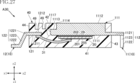
- FIG. 27 is a cross-sectional view showing a semiconductor device according to a third embodiment of the present disclosure.
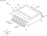
- FIG. 28 is a perspective view showing a semiconductor device according to a fourth embodiment of the present disclosure.
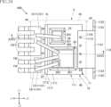
- FIG. 29 is a cross-sectional view showing a semiconductor device according to a fourth embodiment of the present disclosure.
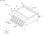
- FIG. 30 is a perspective view showing a semiconductor device according to a fifth embodiment of the present disclosure.
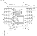
- FIG. 31 is a cross-sectional view showing a semiconductor device according to a fifth embodiment of the present disclosure.
- FIG. 32 is a cross-sectional view showing a semiconductor device according to a sixth embodiment of the present disclosure.
- FIG. 33 is a bottom view of essential parts showing a semiconductor device according to a seventh embodiment of the present disclosure.
- FIG. 34 is a bottom view of essential parts showing a semiconductor device according to an eighth embodiment of the present disclosure.
- FIG. 35 is a cross-sectional view taken along line XXXV-XXXV in FIG. 34.
- FIG. 36 is a cross-sectional view showing a semiconductor device according to a ninth embodiment of the present disclosure.
- FIG. 37 is a perspective view showing a semiconductor device according to a tenth embodiment of the present disclosure.
- FIG. 38 is a bottom view of essential parts showing a semiconductor device according to a tenth embodiment of the present disclosure.
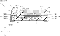
- FIG. 39 is a cross-sectional view showing a semiconductor device according to an eleventh embodiment of the present disclosure.
- FIG. 40 is a cross-sectional view showing a semiconductor device according to a twelfth embodiment of the present disclosure.
- a thing A is formed on a thing B and "a thing A is formed on a thing B” mean “a thing A is formed on a thing B” unless otherwise specified.
- "something A is placed on something B” and “something A is placed on something B” mean "something A is placed on something B” unless otherwise specified.
- First embodiment: 1 to 16 show a semiconductor device according to a first embodiment of the present disclosure.
- the semiconductor device A10 of this embodiment includes a conductive member 10, semiconductor elements 20 and 25, connection members 31, 32, 33, and 34, and a sealing resin 40.
- the semiconductor device A10 has a rectangular shape when viewed in the thickness direction (planar view).
- the thickness direction (planar view direction) of the semiconductor device A10 is defined as the thickness direction z, and the direction along one side of the semiconductor device A10 perpendicular to the thickness direction z (left-right direction in FIGS. 6 and 7) is the first direction x, and the thickness direction z and the direction perpendicular to the first direction x (vertical direction in FIGS. 6 and 7) is the second direction y.
- first side z one side in the thickness direction z
- second side z2 One side of the first direction x (the left side in FIGS. 6 and 7) is defined as a first side x1
- the other side (the right side in FIGS. 6 and 7) is defined as a second side x2.
- One side (lower side in FIG. 6) in the second direction y is defined as a first side y1
- the other side (upper side in FIG. 6) is defined as a second side y2.
- the shape and dimensions of the semiconductor device A10 are not limited.
- the conductive member 10 is a member that constitutes a conductive path to the semiconductor elements 20 and 25.
- the conductive member 10 of this embodiment includes a first lead 11, a second lead 12, a third lead 13, and a fourth lead 14.
- the materials of the first lead 11, second lead 12, third lead 13, and fourth lead 14 are not limited at all, and include, for example, copper (Cu) or a copper alloy. Further, the first lead 11, the second lead 12, the third lead 13, and the fourth lead 14 may be plated with silver (Ag), nickel (Ni), bell (Sn), etc. at appropriate locations. .
- the first lead 11 has a die pad portion 111 and a first terminal portion 112.
- the die pad portion 111 has a first lead main surface 1111 and a first lead back surface 1112.
- the first lead main surface 1111 is a surface facing the first side z1 in the thickness direction z.
- the first lead back surface 1112 is a surface facing the second side z2 in the thickness direction z.
- a semiconductor element 20 is mounted on the first lead main surface 1111.
- the die pad section 111 of this embodiment further includes a first lead side surface 1113, a first intermediate surface 1114, and a contact avoidance surface 1117.
- the first lead side surface 1113 is located between the first lead main surface 1111 and the first lead back surface 1112 in the thickness direction z, and is a surface facing the first side x1 in the first direction x.
- the first intermediate surface 1114 is located between the first lead main surface 1111 and the first lead back surface 1112 in the thickness direction z, and is located on the second side z2 (same as the first lead back surface 1112) in the thickness direction z. side).
- the contact avoidance surface 1117 is located between the first lead main surface 1111 and the first lead back surface 1112 in the thickness direction z, and is connected to the first lead main surface 1111 and the first lead side surface 1113. That is, the contact avoidance surface 1117 is a surface of the die pad portion 111 located on the first side z1 in the thickness direction z and on the first side x1 in the first direction x. The contact avoidance surface 1117 is located on the second side z2 of the first lead main surface 1111 in the thickness direction z. In this embodiment, the contact avoidance surface 1117 is a curved surface that extends to each edge of the die pad portion 111 in the second direction y and is convex outward.
- the shape of the die pad portion 111 is not limited at all.
- the die pad portion 111 has a rectangular shape when viewed in the thickness direction z.
- the shapes of the first lead main surface 1111 and the first lead back surface 1112 are not limited in any way, and in the illustrated example, they are rectangular when viewed in the thickness direction z.
- the first terminal portion 112 is bent toward the first side z1 in the thickness direction z, and includes a first portion 1121, two second portions 1122, and two third portions 1123.
- the first part 1121 is connected to the die pad part 111, extends from the die pad part 111 to the second side x2 in the first direction x, and is parallel (or substantially parallel) to the xy plane in the illustrated example.
- the die pad portion 111 is larger in the thickness direction z than the first portion 1121.
- the first terminal section 112 of this embodiment has only one first section 1121.
- the shape of the first portion 1121 is not limited in any way, and in the illustrated example, it has a rectangular shape when viewed in the thickness direction z.
- the first portion 1121 is separated from the first lead back surface 1112 in the thickness direction z, and is in contact with the first lead main surface 1111 in the illustrated example. One side of the first portion 1121 is flush with the first lead main surface 1111.
- the two second parts 1122 are located on the first side z1 in the thickness direction z with respect to the first part 1121.
- the two second parts 1122 are used when surface mounting the semiconductor device A10 on a circuit board or the like.
- the two third parts 1123 are interposed between the first part 1121 and the two second parts 1122.
- the third portion 1123 extends from the first portion 1121 to the first side z1 in the thickness direction z.
- the third portion 1123 is inclined with respect to the thickness direction z so as to extend outward from the first portion 1121 in the second direction y.
- the shape of the third portion 1123 is not limited at all, and in the illustrated example, it has a rectangular shape when viewed in the first direction x.
- the two second parts 1122 extend outward in the second direction y from the two third parts 1123. Further, the two second portions 1122 are parallel (or substantially parallel) to the second direction y. The two second parts 1122 do not protrude from the two third parts 1123 to the second side x2 in the first direction x. In the illustrated example, the two second parts 1122 and the two third parts 1123 are at the same (or substantially the same) position in the first direction x.
- the second lead 12 is arranged apart from the first lead 11 and is located on the first side x1 in the first direction x with respect to the die pad portion 111.
- the second lead 12 has a second pad portion 121 and a plurality of second terminal portions 122.
- the second pad portion 121 has a second lead main surface 1211 and a second lead back surface 1212.
- the second lead main surface 1211 is a surface facing the first side z1 in the thickness direction z.
- the second lead back surface 1212 is a surface facing the second side z2 in the thickness direction z.
- the second lead main surface 1211 is located at the same (or substantially the same) position as the first lead main surface 1111 in the thickness direction z.
- the connecting member 31 is electrically connected to the second lead main surface 1211.
- the shape of the second pad portion 121 is not limited at all, and in the illustrated example, it is a long rectangular shape whose longitudinal direction is the second direction y.
- the second pad portion 121 is smaller than the die pad portion 111 when viewed in the thickness direction z. Further, the second pad portion 121 has a smaller size in the thickness direction z than the die pad portion 111, and is the same (or approximately the same) as the first terminal portion 112.
- the plurality of second terminal portions 122 are arranged in line in the second direction y.
- the second terminal portion 122 is bent toward the first side z1 in the thickness direction z, and includes a fourth portion 1221, a fifth portion 1222, and a sixth portion 1223.
- the fourth portion 1221 is connected to the second pad portion 121, extends from the second pad portion 121 to the first side x1 in the first direction x, and is parallel (or approximately parallel) to the xy plane in the illustrated example. ).
- the surface of the fourth portion 1221 facing the first side z1 in the thickness direction z is flush with the second lead main surface 1211.
- the shape of the fourth portion 1221 is not limited in any way, and in the illustrated example, it has a rectangular shape when viewed in the thickness direction z.
- the fifth part 1222 is located on the first side z1 in the thickness direction z with respect to the fourth part 1221.
- the fifth portion 1222 is used when surface mounting the semiconductor device A10 on a circuit board or the like.
- the fifth portion 1222 has a shape extending along the first direction x.
- the sixth part 1223 is interposed between the fourth part 1221 and the fifth part 1222.
- the sixth portion 1223 extends from the fourth portion 1221 to the first side z1 in the thickness direction z.
- the sixth portion 1223 is inclined with respect to the thickness direction z (yz plane).
- the shape of the sixth portion 1223 is not limited in any way, and in the illustrated example, it has a rectangular shape when viewed in the first direction x.
- the third lead 13 is arranged apart from the first lead 11 and the second lead 12, and is located on the first side x1 in the first direction x with respect to the die pad portion 111. Furthermore, the third lead 13 is aligned with the second lead 12 in the second direction y.
- the third lead 13 has a third pad portion 131 and a third terminal portion 132.
- the third pad portion 131 has a third lead main surface 1311 and a third lead back surface 1312.
- the third lead main surface 1311 is a surface facing the first side z1 in the thickness direction z.
- the third lead back surface 1312 is a surface facing the second side z2 in the thickness direction z.
- the third lead main surface 1311 is located at the same (or substantially the same) position as the first lead main surface 1111 in the thickness direction z.
- a connecting member 32 is electrically connected to the third lead main surface 1311.
- the shape of the third pad portion 131 is not limited in any way, and in the illustrated example, it has a rectangular shape when viewed in the thickness direction z.
- the third pad portion 131 is smaller than the second pad portion 121 when viewed in the thickness direction z. Further, the third pad section 131 has a smaller size in the thickness direction z than the die pad section 111, and is the same (or approximately the same) as the second pad section 121.
- the third terminal portion 132 is bent toward the first side z1 in the thickness direction z, and includes a seventh portion 1321, an eighth portion 1322, and a ninth portion 1323.
- the seventh portion 1321 is connected to the third pad portion 131, extends from the third pad portion 131 to the first side x1 in the first direction x, and is parallel (or approximately parallel) to the xy plane in the illustrated example. ).
- the surface of the seventh portion 1321 facing the first side z1 in the thickness direction z is flush with the third lead main surface 1311.
- the shape of the seventh portion 1321 is not limited at all, and in the illustrated example, it has a rectangular shape when viewed in the thickness direction z.
- the eighth part 1322 is located on the first side z1 in the thickness direction z with respect to the seventh part 1321.
- the eighth portion 1322 is used when surface mounting the semiconductor device A10 on a circuit board or the like.
- the eighth portion 1322 has a shape extending along the first direction x.
- the ninth part 1323 is interposed between the seventh part 1321 and the eighth part 1322.
- the ninth portion 1323 extends from the seventh portion 1321 to the first side z1 in the thickness direction z.
- the ninth portion 1323 is inclined with respect to the thickness direction z (yz plane).
- the shape of the ninth portion 1323 is not limited in any way, and in the illustrated example, it has a rectangular shape when viewed in the first direction x.
- the fourth lead 14 is arranged apart from the first lead 11, the second lead 12, and the third lead 13, and is located on the first side x1 in the first direction x with respect to the die pad portion 111. Further, the fourth lead 14 is located between the second lead 12 and the third lead 13 in the second direction y.
- the fourth lead 14 has a fourth pad portion 141 and a fourth terminal portion 142.
- the fourth pad portion 141 has a fourth lead main surface 1411 and a fourth lead back surface 1412.
- the fourth lead main surface 1411 is a surface facing the first side z1 in the thickness direction z.
- the fourth lead back surface 1412 is a surface facing the second side z2 in the thickness direction z.
- the fourth lead main surface 1411 is located at the same (or substantially the same) position as the first lead main surface 1111 in the thickness direction z.
- a connecting member 33 is electrically connected to the fourth lead main surface 1411.
- the shape of the fourth pad portion 141 is not limited in any way, and in the illustrated example, it has a rectangular shape when viewed in the thickness direction z.
- the fourth pad section 141 when viewed in the thickness direction z, is smaller than the second pad section 121 and has a size comparable to that of the third pad section 131. Further, the fourth pad section 141 has a smaller size in the thickness direction z than the die pad section 111, and is the same (or approximately the same) as the second pad section 121 and the third pad section 131.
- the fourth terminal portion 142 is bent toward the first side z1 in the thickness direction z, and includes a tenth portion 1421, an eleventh portion 1422, and a twelfth portion 1423.
- the tenth part 1421 is connected to the fourth pad part 141, extends from the fourth pad part 141 to the first side x1 in the first direction x, and is parallel (or approximately parallel) to the xy plane in the illustrated example. ).
- the surface of the tenth portion 1421 facing the first side z1 in the thickness direction z is flush with the fourth lead main surface 1411.
- the shape of the tenth portion 1421 is not limited in any way, and in the illustrated example, it is rectangular when viewed in the thickness direction z.
- the eleventh part 1422 is located on the first side z1 in the thickness direction z with respect to the tenth part 1421.
- the eleventh portion 1422 is used when surface mounting the semiconductor device A10 on a circuit board or the like.
- the eleventh portion 1422 has a shape extending along the first direction x.
- the twelfth part 1423 is interposed between the tenth part 1421 and the eleventh part 1422.
- the twelfth portion 1423 extends from the tenth portion 1421 to the first side z1 in the thickness direction z.
- the twelfth portion 1423 is inclined with respect to the thickness direction z (yz plane).
- the shape of the twelfth portion 1423 is not limited at all, and in the illustrated example, it has a rectangular shape when viewed in the first direction x.
- the semiconductor element 20 is mounted on the first lead main surface 1111 of the die pad section 111, as shown in FIG. 5 and FIGS. 11 to 17.
- the semiconductor element 20 is a switching element.
- the switching element is, for example, an n-channel type MOSFET (Metal-Oxide-Semiconductor Field-Effect Transistor) with a vertical structure.
- the semiconductor element 20 is not limited to a MOSFET.
- the semiconductor element 20 may be another transistor such as an IGBT (Insulated Gate Bipolar Transistor).
- the semiconductor element 20 has a semiconductor layer 205, a first electrode 201, a second electrode 202, and a third electrode 203.
- the semiconductor layer 205 includes a compound semiconductor substrate.
- the main material of the compound semiconductor substrate is silicon carbide (SiC).
- silicon (Si) may be used as the main material of the compound semiconductor substrate.
- the first electrode 201 is provided on the first side z1 of the semiconductor layer 205 in the thickness direction z (the side facing the first lead main surface 1111 in the thickness direction z).
- the first electrode 201 corresponds to the source electrode of the semiconductor element 20.
- the second electrode 202 is provided on the opposite side from the first electrode 201 in the thickness direction z.
- the second electrode 202 faces the first lead main surface 1111 of the die pad portion 111 of the first lead 11 .
- the second electrode 202 corresponds to the drain electrode of the semiconductor element 20.
- the second electrode 202 is conductively bonded to the first lead main surface 1111 via the bonding layer 29.
- the bonding layer 29 is, for example, solder, silver (Ag) paste, fired silver, or the like.
- the third electrode 203 is provided on the same side as the first electrode 201 in the thickness direction z, and is located away from the first electrode 201.
- the third electrode 203 corresponds to the gate electrode of the semiconductor element 20.
- the area of the third electrode 203 is smaller than the area of the first electrode 201 when viewed in the thickness direction z.
- the semiconductor element 25 is mounted on the first lead main surface 1111 of the die pad section 111.
- the semiconductor element 25 is arranged on the first side y1 of the semiconductor element 20 in the second direction y.
- the semiconductor element 25 is a diode.
- the semiconductor element 25 has a semiconductor layer 255, a first electrode 251, and a second electrode 252.
- the semiconductor layer 255 includes a compound semiconductor substrate.
- the main material of the compound semiconductor substrate is silicon carbide (SiC).
- silicon (Si) may be used as the main material of the compound semiconductor substrate.
- the first electrode 251 is provided on the first side z1 of the semiconductor layer 255 in the thickness direction z (the side facing the first lead main surface 1111 in the thickness direction z).
- the first electrode 251 corresponds to the anode electrode of the semiconductor element 25.
- the second electrode 252 is provided on the opposite side from the first electrode 251 in the thickness direction z.
- the second electrode 252 faces the first lead main surface 1111 of the die pad portion 111 of the first lead 11 .
- the second electrode 252 corresponds to the cathode electrode of the semiconductor element 25.
- the second electrode 252 is conductively bonded to the first lead main surface 1111 via the bonding layer 29.
- connection members 31, 32, 33, 34 The connecting member 31 is electrically connected to the first electrode 201 of the semiconductor element 20 and the second lead main surface 1211 of the second pad portion 121 of the second lead 12 .
- the material of the connecting member 31 is not limited at all, and includes metals such as aluminum (Al), copper (Cu), and gold (Au).
- the connecting member 31 is a wire containing aluminum (Al) and has a relatively large diameter in order to allow a large current to flow therethrough.
- the diameter of the connecting member 31 is not limited, but is, for example, about 400 to 500 ⁇ m.
- the number of connecting members 31 is not limited at all, and a plurality of connecting members 31 may be provided. As shown in FIG. 13, in the first direction It is 1/3 or more of L2. Note that the distance L1 is not limited to this.
- the connecting member 32 is electrically connected to the third electrode 203 of the semiconductor element 20 and the third lead main surface 1311 of the third pad portion 131 of the third lead 13.
- the material and diameter of the connecting member 32 are not limited at all, in this embodiment, the same wire as the connecting member 31 is used.
- the connecting member 33 is electrically connected to the first electrode 201 of the semiconductor element 20 and the fourth lead main surface 1411 of the fourth pad portion 141 of the fourth lead 14. Although the material and diameter of the connecting member 33 are not limited at all, the same wire as the connecting member 31 is used in this embodiment.
- the connecting member 34 is electrically connected to the first electrode 251 of the semiconductor element 25 and the second lead main surface 1211 of the second pad portion 121 of the second lead 12. Although the material and diameter of the connecting member 34 are not limited at all, in this embodiment, the same wire as the connecting member 31 is used.
- the first terminal portion 112 of the first lead 11 is a drain terminal
- the second terminal portion 122 of the second lead 12 is a source terminal
- the third terminal portion 132 of the third lead 13 is a drain terminal.
- the fourth terminal portion 142 of the fourth lead 14 is a source sense terminal.
- Sealing resin 40 As shown in FIGS. 1 to 17, the sealing resin 40 connects the semiconductor elements 20, 25, the connecting members 31, 32, 33, 34, the first lead 11, the second lead 12, the third lead 13, and the third lead 13. It covers a portion of each of the four leads 14.
- the sealing resin 40 has electrical insulation properties.
- the sealing resin 40 is made of a material containing, for example, a black epoxy resin.
- the sealing resin 40 has a first resin surface 41 , a second resin surface 42 , a third resin surface 43 , a fourth resin surface 44 , a fifth resin surface 45 , and a sixth resin surface 46 .
- the first resin surface 41 faces the first side z1 in the thickness direction z (the same side as the first lead main surface 1111 in the thickness direction z). As shown in FIG. 13, the distance L4 between the first resin surface 41 and the first lead main surface 1111 (the thickness dimension of the sealing resin 40 on the first lead main surface 1111) is relatively small. It is 4 times or less of the diameter L3 of 31 to 34. Note that the distance L4 is not limited to this.
- the second resin surface 42 faces the second side z2 in the thickness direction z (the opposite side to the first resin surface 41 in the thickness direction z). A first lead back surface 1112 of the die pad portion 111 of the first lead 11 is exposed from the second resin surface 42 . The second resin surface 42 and the first lead back surface 1112 are flush with each other. The first lead back surface 1112 is separated from the third resin surface 43 in the first direction x.
- the third resin surface 43 faces the second side x2 in the first direction x.
- the first portions 1121 of the plurality of first terminal portions 112 of the first lead 11 penetrate the third resin surface 43 . Further, the first portion 1121 is separated from the second resin surface 42 in the thickness direction z.
- the fourth resin surface 44 faces the first side x1 in the first direction x (the opposite side to the third resin surface 43 in the first direction x).
- the fourth part 1221 of the plurality of second terminal parts 122 of the second lead 12, the seventh part 1321 of the third terminal part 132 of the third lead 13, and the fourth terminal part of the fourth lead 14 are The tenth portion 1421 of 142 penetrates the fourth resin surface 44 . Further, the fourth portion 1221, the seventh portion 1321, and the tenth portion 1421 are separated from the second resin surface 42 in the thickness direction z.
- the fifth resin surface 45 and the sixth resin surface 46 are surfaces facing oppositely to each other in the second direction y.
- the sealing resin 40 has grooves 49.
- the groove 49 is recessed from the second resin surface 42 in the thickness direction z and extends along the second direction y.
- the groove 49 reaches the fifth resin surface 45 and the sixth resin surface 46.
- FIG. 17 shows the usage state of the semiconductor device A10.
- the semiconductor device A10 is surface mounted on the circuit board 92. That is, the second part 1122 of the first terminal part 112, the fifth part 1222 of the second terminal part 122, the eighth part 1322 of the third terminal part 132, and the eleventh part 1422 of the fourth terminal part 142 are, for example, solder 921. It is electrically connected to the wiring pattern (not shown) of the circuit board 92 by means of the circuit board 92 . Further, a heat sink 91 is disposed opposite to the first lead back surface 1112 of the die pad portion 111 . In the illustrated example, a sheet material 919 is disposed between the first lead back surface 1112 and the heat sink 91. The sheet material 919 is, for example, an insulating sheet.
- the die pad portion 111 includes a contact avoidance surface 1117.
- the contact avoidance surface 1117 is connected to the first lead main surface 1111 and the first lead side surface 1113, and is located on the second side z2 of the first lead main surface 1111 in the thickness direction z. All of the connecting members 31 to 34 overlap the contact avoidance surface 1117 when viewed in the thickness direction z. Therefore, in the semiconductor device A10, the connection members 31 to 34 can be prevented from coming into contact with the die pad portion 111, compared to the case where the die pad portion 111 does not include the contact avoidance surface 1117.
- the contact avoidance surface 1117 extends to each edge of the die pad portion 111 in the second direction y. Therefore, in the semiconductor device A10, even when the connecting members 31 to 34 are located near each edge of the die pad portion 111 in the second direction y, the connecting members 31 to 34 can be prevented from coming into contact with the die pad portion 111.
- the first lead back surface 1112 is exposed from the second resin surface 42, as shown in FIGS. 12 to 16.
- the heat sink 91 can be placed opposite the first lead back surface 1112.
- the second portion 1122 is located closer to the first side z1 in the thickness direction z than the first portion 1121 is.
- the first lead back surface 1112 is separated from the third resin surface 43 in the first direction x.
- the first portion 1121 is separated from the second resin surface 42 in the thickness direction z. Therefore, a portion of the sealing resin 40 exists between the first lead back surface 1112 and the first portion 1121. Thereby, the first lead 11 can be held more firmly by the sealing resin 40.
- the third portion 1123 is parallel (or substantially parallel) to the yz plane, and the second portion 1122 does not protrude from the third portion 1123 in the first direction x. Therefore, in the semiconductor device A10, the dimension in the first direction x can be reduced compared to the case where the second portion 1122 protrudes from the third portion 1123 in the first direction x. Further, since the two second portions 1122 extend outward in the first direction x from the third portion 1123, the semiconductor device A10 can further increase the mounting strength.
- the die pad portion 111 is larger in the thickness direction z than the first portion 1121. Therefore, in the process of heat being transmitted from the semiconductor element 20 to the first lead back surface 1112, it is possible to transmit the heat to a wider range in the first direction x and the second direction y. Therefore, the wider area of the first lead back surface 1112 allows heat from the semiconductor element 20 to be radiated to the heat sink 91 and the like, thereby increasing heat radiation efficiency.
- the groove 49 is formed in the sealing resin 40.
- the surface of the sealing resin 40 from the first lead back surface 1112 to the second lead 12 (fourth part 1221), third lead 13 (seventh part 1321), and fourth lead 14 (tenth part 1421) (hereinafter referred to as creepage distance) can be extended.
- the semiconductor element 20 and the semiconductor element 25 are mounted on the first lead main surface 1111 of the die pad portion 111, but the present invention is not limited to this.
- the type and number of semiconductor elements mounted on the first lead main surface 1111 are not limited, and other electronic components may be mounted.
- FIG. 18 shows a first modification of the semiconductor device A10.
- the shape of the contact avoidance surface 1117 is different from the above-described example.
- the contact avoidance surface 1117 is a plane that is inclined with respect to the first lead main surface 1111 and the first lead side surface 1113.
- the semiconductor device A11 can suppress the connection members 31 to 34 from coming into contact with the die pad portion 111, and has the same effect as the semiconductor device A10.
- FIG. 19 shows a second modification of the semiconductor device A10.
- the shape of the contact avoidance surface 1117 is different from the above-described example.
- the contact avoidance surface 1117 includes a first surface 1117a that is connected to the first lead main surface 1111 and parallel (or approximately parallel) to the first lead side surface 1113, and a first surface 1117a that is connected to the first lead side surface 1113 and is parallel to the first lead side surface 1113 and A second surface 1117b parallel (or substantially parallel) to the main lead surface 1111 is included.
- the contact avoidance surface 1117 is a step in the die pad portion 111 that is recessed from the first lead main surface 1111 to the second side z2 in the thickness direction z and recessed from the first lead side surface 1113 to the second side x2 in the first direction x. It forms a shaped recess.
- the semiconductor device A12 can suppress the connection members 31 to 34 from coming into contact with the die pad portion 111, and has the same effect as the semiconductor device A10.
- FIG. 20 shows a third modification of the semiconductor device A10.
- the shape of the contact avoidance surface 1117 is different from the above-described example.
- the contact avoidance surface 1117 includes a first surface 1117a that is connected to the first lead main surface 1111 and parallel (or approximately parallel) to the first lead side surface 1113, and a first surface 1117a that is connected to the first lead surface 1117a and that is parallel to the first lead side surface 1113 and It includes a second surface 1117b that is parallel (or substantially parallel) to the main surface 1111, and a third surface 1117c that is a curved surface connected to the second surface 1117b and the first lead side surface 1113.
- the portion sandwiched between the second surface 1117b and the third surface 1117c is a portion that is crushed by the crushing process and extends outward. Also in this modification, the semiconductor device A13 can suppress the connection members 31 to 34 from coming into contact with the die pad portion 111, and has the same effect as the semiconductor device A10.
- FIG. 21 shows a fourth modification of the semiconductor device A10.
- the shape of the contact avoidance surface 1117 is different from the above-described example.
- the contact avoidance surface 1117 is a concave curved surface.
- the contact avoidance surface 1117 forms a recess in the die pad portion 111 that is recessed from the first lead main surface 1111 to the second side z2 in the thickness direction z and recessed from the first lead side surface 1113 to the second side x2 in the first direction x. are doing.
- the recess (contact avoidance surface 1117) is formed, for example, by etching.
- the semiconductor device A14 can suppress the connection members 31 to 34 from coming into contact with the die pad portion 111, and has the same effect as the semiconductor device A10.
- FIG. 22 shows a fifth modification of the semiconductor device A10.
- the shape of the contact avoidance surface 1117 is different from the above-described example.
- the contact avoidance surface 1117 is a combination of the contact avoidance surface 1117 according to the second modification and the contact avoidance surface 1117 according to the third modification, and has a stepped shape.
- the semiconductor device A15 can suppress the connection members 31 to 34 from coming into contact with the die pad portion 111, and has the same effect as the semiconductor device A10.
- the shape of the contact avoidance surface 1117 is not limited.
- the contact avoidance surface 1117 may be located on the second side z2 of the first lead main surface 1111 in the thickness direction z.
- FIG. 23 shows a sixth modification of the semiconductor device A10.
- the semiconductor device A16 of this modification differs from the above-described example in the range in which the contact avoidance surface 1117 is arranged. Note that each part of the first to fifth modifications described above may be combined arbitrarily.
- the contact avoidance surface 1117 is located inside the die pad portion 111 in the second direction y. In other words, the contact avoidance surface 1117 does not extend to each edge of the die pad portion 111 in the second direction y. However, the contact avoidance surface 1117 overlaps all of the connecting members 31 to 34 when viewed in the thickness direction z.
- the arrangement position of the contact avoidance surface 1117 in the second direction y is not limited as long as it overlaps all of the connecting members 31 to 34 when viewed in the thickness direction z.
- the semiconductor device A16 can suppress the connection members 31 to 34 from coming into contact with the die pad portion 111, and has the same effect as the semiconductor device A10. Furthermore, according to this modification, the semiconductor device A16 has a smaller area of the contact avoidance surface 1117 compared to the case where the contact avoidance surface 1117 extends to each edge of the die pad portion 111 in the second direction y. , the area of the first lead main surface 1111 can be increased.
- Second embodiment: 24 and 25 show a semiconductor device according to a second embodiment of the present disclosure.
- the semiconductor device A20 of this embodiment differs from the first embodiment in the relationship between the second portion 1122, the fifth portion 1222, the eighth portion 1322, and the eleventh portion 1422 and the first resin surface 41.
- the configuration and operation of other parts of this embodiment are similar to those of the first embodiment. Note that each part of the first embodiment and each modification example described above may be combined arbitrarily.
- the second part 1122, the fifth part 1222, the eighth part 1322, and the eleventh part 1422 are located on the second side z2 in the thickness direction z (the first lead back surface 1112 is It is located on the opposite side).
- the surfaces of the second portion 1122, the fifth portion 1222, the eighth portion 1322, and the eleventh portion 1422 facing the first side z1 in the thickness direction z and the first resin surface 41 are separated by a distance Gz.
- the semiconductor device A20 can suppress the connection members 31 to 34 from coming into contact with the die pad portion 111, and has the same effect as the semiconductor device A10. Further, the first resin surface 41 protrudes from the second portion 1122, the fifth portion 1222, the eighth portion 1322, and the eleventh portion 1422 by a distance Gz toward the first side z1 in the thickness direction z. Therefore, in the usage state of the semiconductor device A11 shown in FIG. 25, when the heat sink 91 is pressed against the semiconductor device A20, the first resin surface 41 easily comes into contact with the circuit board 92. Thereby, the force applied from the heat sink 91 can be suppressed from acting on the first lead 11 , the second lead 12 , the third lead 13 , the fourth lead 14 and the semiconductor element 20 .
- Third embodiment 26 and 27 show a semiconductor device according to a third embodiment of the present disclosure.
- the semiconductor device A30 of this embodiment differs from the first embodiment in that two grooves 49 are provided in the sealing resin 40.
- the configuration and operation of other parts of this embodiment are similar to those of the first embodiment. Note that each part of the first to second embodiments and each modification example described above may be combined arbitrarily.
- Each groove 49 extends in the second direction y and reaches the fifth resin surface 45 and the sixth resin surface 46. Further, the two grooves 49 are arranged apart from each other in the first direction x.
- the semiconductor device A30 can suppress the connection members 31 to 34 from coming into contact with the die pad portion 111, and has the same effect as the semiconductor device A10. Furthermore, by having the two grooves 49, the creepage distance between the first lead back surface 1112 and the second terminal section 122, third terminal section 132, and fourth terminal section 142 can be further extended. As understood from this embodiment, the number of grooves 49 is not limited at all.
- Fourth embodiment 28 and 29 show a semiconductor device according to a fourth embodiment of the present disclosure.
- the semiconductor device A40 of this embodiment differs from the first embodiment in that a convex portion 48 is provided in the sealing resin 40.
- the configuration and operation of other parts of this embodiment are similar to those of the first embodiment. Note that each part of the first to third embodiments and each modification example described above may be combined arbitrarily.
- the convex portion 48 protrudes from the second resin surface 42 toward the second side z2 in the thickness direction z.
- the convex portion 48 extends along the second direction y and reaches the fifth resin surface 45 and the sixth resin surface 46.
- the convex portion 48 is disposed at the first side x1 end of the sealing resin 40 in the first direction x, and is in contact with the fourth resin surface 44 .
- the semiconductor device A40 can suppress the connection members 31 to 34 from coming into contact with the die pad portion 111, and has the same effect as the semiconductor device A10. Further, by having the convex portion 48, the creeping distance between the first lead back surface 1112 and the second terminal portion 122, third terminal portion 132, and fourth terminal portion 142 can be extended.
- Fifth embodiment 30 and 31 show a semiconductor device according to a fifth embodiment of the present disclosure.
- the semiconductor device A50 of this embodiment differs from the first embodiment in that two convex portions 48 are provided on the sealing resin 40.
- the configuration and operation of other parts of this embodiment are similar to those of the first embodiment. Note that each part of the above-described first to fourth embodiments and each modification may be arbitrarily combined.
- Each of the protrusions 48 protrudes from the second resin surface 42 toward the second side z2 in the thickness direction z.
- Each convex portion 48 extends along the second direction y and reaches the fifth resin surface 45 and the sixth resin surface 46.
- the two convex portions 48 are arranged apart from each other with the first lead back surface 1112 in between in the first direction x.
- One convex portion 48 is in contact with the fourth resin surface 44 .
- the other convex portion 48 is in contact with the third resin surface 43.
- the semiconductor device A50 can suppress the connection members 31 to 34 from coming into contact with the die pad portion 111, and has the same effect as the semiconductor device A10. Further, by having the two convex portions 48, the creepage distance between the first lead back surface 1112 and the second terminal portion 122, third terminal portion 132, and fourth terminal portion 142 can be further extended. As understood from this embodiment, the number of convex portions 48 is not limited at all.
- FIG. 32 shows a semiconductor device according to a sixth embodiment of the present disclosure.
- the semiconductor device A60 of this embodiment differs from the first embodiment in that the sealing resin 40 does not have the groove 49.
- the configuration and operation of other parts of this embodiment are similar to those of the first embodiment. Note that each part of the above-described first to fifth embodiments and each modification may be arbitrarily combined.
- the semiconductor device A60 can suppress the connection members 31 to 34 from coming into contact with the die pad portion 111, and has the same effect as the semiconductor device A10.
- the sealing resin 40 may have a configuration in which the convex portion 48 and the groove 49 are not provided.
- FIG. 33 shows a semiconductor device according to a seventh embodiment of the present disclosure.
- the semiconductor device A70 of this embodiment differs from the first embodiment in that it does not include the semiconductor element 25.
- the configuration and operation of other parts of this embodiment are similar to those of the first embodiment. Note that each part of the above-described first to sixth embodiments and each modification may be arbitrarily combined.
- the semiconductor device A70 can suppress the connection members 31 to 34 from coming into contact with the die pad portion 111, and has the same effect as the semiconductor device A10. Further, as understood from this embodiment, the type and number of electronic components mounted on the first lead main surface 1111 are not limited.
- Eighth embodiment: 34 and 35 show a semiconductor device according to an eighth embodiment of the present disclosure.
- the semiconductor device A80 of this embodiment differs from the first embodiment in that the first lead 11 is formed by joining the die pad part 111 and the first terminal part 112.
- the configuration and operation of other parts of this embodiment are similar to those of the first embodiment. Note that each part of the above-described first to seventh embodiments and each modification may be arbitrarily combined.
- the first lead 11 is formed by joining a die pad part 111 and a first terminal part 112, which were separate members.
- the die pad section 111 includes a plurality of engagement sections 1115 that protrude from the first lead main surface 1111 in the thickness direction z and are engaged with engagement holes 1125 (described later) of the first terminal section 112. .
- the plurality of engaging portions 1115 are arranged in line in the second direction y.
- a first portion 1121 of the first terminal portion 112 is joined to the die pad portion 111.
- the first portion 1121 is bonded to the first lead main surface 1111 of the die pad portion 111.
- the first part 1121 has a plurality of engagement holes 1125 penetrating in the thickness direction z.
- the plurality of engagement holes 1125 are arranged in line in the second direction y.
- the first part 1121 is caulked to the die pad part 111. Specifically, in the first portion 1121, the engaging portion 1115 of the die pad portion 111 is inserted into the engaging hole 1125. Then, while applying heat, pressure is applied from the distal end side of the engaging portion 1115 using a mold. As a result, the distal end portion of the engaging portion 1115 is crushed and engaged with the engaging hole 1125, and the circumferential surface of the engaging portion 1115 is brought into close contact with the inner surface of the engaging hole 1125.
- the semiconductor device A80 can suppress the connection members 31 to 34 from coming into contact with the die pad portion 111, and has the same effect as the semiconductor device A10.
- the first lead 11 is formed by joining the die pad portion 111 and the first terminal portion 112, which were separate members. Therefore, it is possible to form the first lead 11 having the die pad portion 111 and the first terminal portion 112 that are significantly different in size in the thickness direction z.
- the first lead 11 using a lead frame with irregularly shaped strips, there is a limit on the dimension of the die pad section 111 in the thickness direction z. The dimension in the horizontal direction z can be increased.
- the first lead 11 is formed by inserting each engaging portion 1115 of the die pad portion 111 into each engaging hole 1125 of the first portion 1121 of the first terminal portion 112 and joining by caulking.
- the first lead 11 is an integral member in which the first terminal portion 112 is firmly joined to the die pad portion 111. Therefore, in joining the die pad section 111 and the first terminal section 112, there is no need to use other members such as a bonding material.
- the method of joining the die pad portion 111 and the first terminal portion 112 is not limited.
- the die pad portion 111 and the first terminal portion 112 may be joined by other mechanical joining using components such as screws and rivets.
- the die pad section 111 and the first terminal section 112 may be joined by ultrasonic bonding, for example, by a bonding material such as solder, silver (Ag) paste, or baked silver, or by welding. They may also be joined by other metallurgical joining such as.
- a bonding material such as solder, silver (Ag) paste, or baked silver, or by welding. They may also be joined by other metallurgical joining such as.
- FIG. 36 shows a semiconductor device according to a ninth embodiment of the present disclosure.
- the semiconductor device A90 of this embodiment is different from the above-described embodiments in the configuration of the first lead 11.
- the configuration and operation of other parts of this embodiment are similar to those of the first embodiment. Note that each part of the above-described first to eighth embodiments and each modification may be arbitrarily combined.
- the die pad section 111 includes a first lead second side surface 1116.
- the first lead second side surface 1116 is located between the first lead main surface 1111 and the first lead back surface 1112 in the thickness direction z, and is a surface facing the second side x2 in the first direction x.
- the first lead second side surface 1116 is located on the second side x2 in the first direction x from the third resin surface 43. That is, the first lead second side surface 1116 has a portion located on the second side x2 in the first direction x from the third resin surface 43 when viewed in the thickness direction z.
- the semiconductor device A90 can suppress the connection members 31 to 34 from coming into contact with the die pad portion 111, and has the same effect as the semiconductor device A10. Further, according to the present embodiment, since the first lead back surface 1112 has a portion protruding from the third resin surface 43 to the second side x2 in the first direction x, the area of the first lead back surface 1112 facing the heat sink 91 is It is possible to expand. Therefore, the efficiency of heat radiation from the semiconductor device A90 to the heat sink 91 can be increased.
- Tenth embodiment 37 and 38 show a semiconductor device according to a tenth embodiment of the present disclosure.
- the semiconductor device A100 of this embodiment is different from the above-described embodiments in the configuration of the first terminal section 112.
- the configuration and operation of other parts of this embodiment are similar to those of the first embodiment. Note that each part of the above-described first to ninth embodiments and each modification may be arbitrarily combined.
- the first lead 11 of this embodiment has a plurality of first terminal portions 112.
- the plurality of first terminal parts 112 are arranged in line in the second direction y.
- Each first terminal section 112 has a first section 1121, a second section 1122, and a third section 1123.
- the first part 1121 is connected to the die pad part 111.
- the first portion 1121 extends from the first lead second side surface 1116 of the die pad portion 111 to the second side x2 in the first direction x, and is parallel (or substantially parallel) to the xy plane in the illustrated example.
- the first portion 1121 penetrates the third resin surface 43.
- the shape of the first portion 1121 is not limited at all, and in the illustrated example, it is rectangular when viewed in the thickness direction z.
- the second part 1122 is located on the first side z1 in the thickness direction z with respect to the first part 1121.
- the second portion 1122 is used when surface mounting the semiconductor device A100 on a circuit board or the like.
- the second portion 1122 has a shape extending along the first direction x.
- the third part 1123 is interposed between the first part 1121 and the second part 1122.
- the third portion 1123 extends from the first portion 1121 to the first side z1 in the thickness direction z.
- the third portion 1123 is inclined with respect to the thickness direction z (yz plane).
- the shape of the third portion 1123 is not limited at all, and in the illustrated example, it has a rectangular shape when viewed in the first direction x.
- the semiconductor device A100 can suppress the connection members 31 to 34 from coming into contact with the die pad portion 111, and has the same effect as the semiconductor device A10. Furthermore, the first lead 11 has a plurality of first terminal portions 112. Thereby, the mounting strength of the semiconductor device A100 can be increased. As understood from this embodiment, the configuration of the first terminal portion 112 is not limited at all.
- FIG. 39 shows a semiconductor device according to an eleventh embodiment of the present disclosure.
- the shapes of the first terminal section 112, the second terminal section 122, the third terminal section 132, and the fourth terminal section 142 are different from those of the above-described embodiments.
- the configuration and operation of other parts of this embodiment are similar to those of the first embodiment. Note that each part of the above-described first to tenth embodiments and each modification may be arbitrarily combined.
- the third portion 1123 extends from the second side x2 end in the first direction x of the first portion 1121 to the first side in the thickness direction z along the third resin surface 43. Extends to z1. Further, the second portion 1122 extends from the first side z1 end of the third portion 1123 in the thickness direction z to the first side x1 in the first direction x along the first resin surface 41. In the second terminal portion 122 of the present embodiment, the sixth portion 1223 extends from the first side x1 end in the first direction x of the fourth portion 1221 along the fourth resin surface 44 in the thickness direction z. Extends to the first side z1.
- the fifth portion 1222 extends from the first side z1 end in the thickness direction z of the sixth portion 1223 to the second side x2 in the first direction x along the first resin surface 41.
- the ninth portion 1323 extends from the second side x2 end in the first direction x of the seventh portion 1321 to the fourth resin surface 44. along the first side z1 in the thickness direction z.
- the eighth portion 1322 extends from the first side z1 end of the ninth portion 1323 in the thickness direction z to the second side x2 in the first direction x along the first resin surface 41.
- the twelfth portion 1423 extends from the second side x2 end in the first direction x of the tenth portion 1421 along the fourth resin surface 44 in the thickness direction z. Extends to the first side z1. Further, the eleventh portion 1422 extends from the first side z1 end of the twelfth portion 1423 in the thickness direction z to the second side x2 in the first direction x along the first resin surface 41.
- the semiconductor device A110 can suppress the connection members 31 to 34 from coming into contact with the die pad portion 111, and has the same effect as the semiconductor device A10.
- the second part 1122, the fifth part 1222, the eighth part 1322, and the eleventh part 1422 extend inward in the first direction x, so they extend outward in the first direction x.
- the mounting area (dimension in the first direction x) of the semiconductor device A110 can be reduced compared to the case where the semiconductor device A110 extends toward the direction (so-called gull wing shape).
- the shapes of the first terminal section 112, the second terminal section 122, the third terminal section 132, and the fourth terminal section 142 are not limited at all.
- FIG. 40 shows a semiconductor device according to a twelfth embodiment of the present disclosure.
- the semiconductor device A120 of this embodiment is different from the above-described embodiments in the configurations of the first terminal section 112, the second terminal section 122, the third terminal section 132, and the fourth terminal section 142.
- the configuration and operation of other parts of this embodiment are similar to those of the first embodiment. Note that each part of the above-described first to eleventh embodiments and each modification may be arbitrarily combined.
- the first portion 1121 does not penetrate the third resin surface 43, the third portion 1123 extends within the sealing resin 40 in the thickness direction z, and the second portion 1122 is exposed from the first resin surface 41.
- the fourth portion 1221 does not penetrate the fourth resin surface 44, the sixth portion 1223 extends within the sealing resin 40 in the thickness direction z, and the fifth portion 1222 extends through the first resin surface 44. It is exposed from the surface 41.
- the seventh portion 1321 does not penetrate the fourth resin surface 44
- the ninth portion 1323 extends within the sealing resin 40 in the thickness direction z
- the third terminal portion 132 Eight portions 1322 are exposed from the first resin surface 41.
- the tenth portion 1421 does not penetrate the fourth resin surface 44
- the twelfth portion 1423 extends within the sealing resin 40 in the thickness direction z
- the eleventh portion 1422 extends through the first resin surface 44. It is exposed from the resin surface 41.
- the semiconductor device A120 can suppress the connection members 31 to 34 from coming into contact with the die pad portion 111, and has the same effect as the semiconductor device A10. Further, the first terminal portion 112, the second terminal portion 122, the third terminal portion 132, and the fourth terminal portion 142 may penetrate the third resin surface 43 or the fourth resin surface 44 and protrude in the first direction x. In comparison, the mounting area (dimension in the first direction x) of the semiconductor device A120 can be reduced. As understood from this embodiment, the configurations of the first terminal section 112, the second terminal section 122, the third terminal section 132, and the fourth terminal section 142 are not limited at all.
- the semiconductor device according to the present disclosure is not limited to the embodiments described above.
- the specific configuration of each part of the semiconductor device according to the present disclosure can be changed in design in various ways.
- the present disclosure includes the embodiments described in the appendix below.
- the die pad section further includes a contact avoidance surface (1117) connected to the first lead main surface and the first lead side surface, The contact avoidance surface overlaps the wire when viewed in the thickness direction, and is located on a second side of the first lead main surface in the thickness direction.
- the contact avoidance surface is an outwardly convex curved surface, The semiconductor device according to supplementary note 1. Supplementary Note 3, Fourth Modification of First Embodiment, FIG. 21.
- the contact avoidance surface is a concave curved surface.
- the contact avoidance surface is a plane inclined with respect to the first lead main surface and the first lead side surface.
- Supplementary Note 5 Second Modification of First Embodiment, FIG.
- the contact avoidance surfaces include a first surface (1117a) connected to the first lead main surface and parallel to the first lead side surface, and a second surface (1117a) connected to the first lead side surface and parallel to the first lead main surface.
- (1117b) The semiconductor device according to supplementary note 1.
- the contact avoidance surface is located inside the die pad portion in a second direction (y) perpendicular to the thickness direction and the first direction.
- Appendix 7. The contact avoidance surface extends to an edge of the die pad portion in a second direction perpendicular to the thickness direction and the first direction.
- Appendix 8. the second lead is bent toward the first side in the thickness direction;
- the semiconductor device according to any one of Supplementary Notes 1 to 7. Appendix 9, Figure 13.
- a distance (L1) between the first lead side surface and a bonding position of the wire of the semiconductor element is 1/3 or more of a dimension (L2) of the first lead main surface;
- the semiconductor device according to any one of Supplementary Notes 1 to 8. Appendix 10.
- the semiconductor device according to any one of Supplementary Notes 1 to 9. Appendix 11, Figure 13.
- the distance (L4) between the first resin surface and the first lead main surface is four times or less the diameter (L3) of the wire,
- the semiconductor device according to appendix 10.
- the first lead further includes a first terminal portion (112),
- the first terminal portion includes a first portion (1121) connected to the die pad portion, and a second portion (1122) located on a first side in the thickness direction with respect to the first portion and used for mounting.
- the first lead further includes a first terminal portion, The first terminal portion includes a first portion joined to the die pad portion, a second portion located on a first side in the thickness direction with respect to the first portion and used for mounting, and the first portion. and a third part interposed between the third part and the second part.
- the die pad section further includes an engaging section (1115),
- the first part has an engagement hole (1125) that engages with the engagement part, the engagement portion is caulked into the engagement hole;
- Appendix 12-3. the first portion is joined to the first lead main surface;
- Appendix 13
- the second lead includes a second pad portion (121) and a second terminal portion (122) connected to the second pad portion,
- the second terminal portion includes a fourth portion (1221) connected to the second pad portion, and a fifth portion (1222) located on the first side in the thickness direction with respect to the fourth portion and used for mounting.
- the sealing resin further includes a third resin surface (43) facing the first side in the first direction, and a fourth resin surface (44) facing the second side in the first direction.
- Appendix 14. The first part penetrates the third resin surface and is separated from the second resin surface in the thickness direction, The fourth part penetrates the fourth resin surface and is separated from the second resin surface in the thickness direction.
- the semiconductor device according to appendix 13. Supplementary Note 15, Second Embodiment, FIGS. 24, 25.
- the second part and the fifth part are located on a second side in the thickness direction from the first resin surface.
- the second pad portion has a second lead main surface facing the first side in the thickness direction,
- the first side surface in the thickness direction of the first part, the first lead main surface, the first side surface in the thickness direction of the fourth part, and the second lead main surface are At the same position in the thickness direction,
- the third part and the sixth part extend in the thickness direction within the sealing resin, the second part and the fifth part are exposed from the first resin surface;
- the sealing resin has a groove (49) recessed from the second resin surface in the thickness direction.
- Supplementary Note 19, Fourth Embodiment, FIGS. 28 and 29. 19 The semiconductor device according to any one of appendices 10 to 18, wherein the sealing resin has a convex portion (48) protruding from the second resin surface in the thickness
- Semiconductor device 10 Conductive member 11: First lead 12: No.
Landscapes
- Lead Frames For Integrated Circuits (AREA)
- Structures Or Materials For Encapsulating Or Coating Semiconductor Devices Or Solid State Devices (AREA)
Priority Applications (2)
| Application Number | Priority Date | Filing Date | Title |
|---|---|---|---|
| JP2024546803A JPWO2024057838A1 (https=) | 2022-09-14 | 2023-08-22 | |
| US19/076,503 US20250210475A1 (en) | 2022-09-14 | 2025-03-11 | Semiconductor device |
Applications Claiming Priority (2)
| Application Number | Priority Date | Filing Date | Title |
|---|---|---|---|
| JP2022-146346 | 2022-09-14 | ||
| JP2022146346 | 2022-09-14 |
Related Child Applications (1)
| Application Number | Title | Priority Date | Filing Date |
|---|---|---|---|
| US19/076,503 Continuation US20250210475A1 (en) | 2022-09-14 | 2025-03-11 | Semiconductor device |
Publications (1)
| Publication Number | Publication Date |
|---|---|
| WO2024057838A1 true WO2024057838A1 (ja) | 2024-03-21 |
Family
ID=90274851
Family Applications (1)
| Application Number | Title | Priority Date | Filing Date |
|---|---|---|---|
| PCT/JP2023/030130 Ceased WO2024057838A1 (ja) | 2022-09-14 | 2023-08-22 | 半導体装置 |
Country Status (3)
| Country | Link |
|---|---|
| US (1) | US20250210475A1 (https=) |
| JP (1) | JPWO2024057838A1 (https=) |
| WO (1) | WO2024057838A1 (https=) |
Citations (4)
| Publication number | Priority date | Publication date | Assignee | Title |
|---|---|---|---|---|
| JPH0437050A (ja) * | 1990-05-31 | 1992-02-07 | Hitachi Ltd | 樹脂封止型半導体装置 |
| US5585667A (en) * | 1994-12-23 | 1996-12-17 | National Semiconductor Corporation | Lead frame for handling crossing bonding wires |
| JP2011054626A (ja) * | 2009-08-31 | 2011-03-17 | Sanyo Electric Co Ltd | 半導体装置およびその製造方法 |
| JP2017135241A (ja) * | 2016-01-27 | 2017-08-03 | ローム株式会社 | 半導体装置 |
-
2023
- 2023-08-22 JP JP2024546803A patent/JPWO2024057838A1/ja active Pending
- 2023-08-22 WO PCT/JP2023/030130 patent/WO2024057838A1/ja not_active Ceased
-
2025
- 2025-03-11 US US19/076,503 patent/US20250210475A1/en active Pending
Patent Citations (4)
| Publication number | Priority date | Publication date | Assignee | Title |
|---|---|---|---|---|
| JPH0437050A (ja) * | 1990-05-31 | 1992-02-07 | Hitachi Ltd | 樹脂封止型半導体装置 |
| US5585667A (en) * | 1994-12-23 | 1996-12-17 | National Semiconductor Corporation | Lead frame for handling crossing bonding wires |
| JP2011054626A (ja) * | 2009-08-31 | 2011-03-17 | Sanyo Electric Co Ltd | 半導体装置およびその製造方法 |
| JP2017135241A (ja) * | 2016-01-27 | 2017-08-03 | ローム株式会社 | 半導体装置 |
Also Published As
| Publication number | Publication date |
|---|---|
| US20250210475A1 (en) | 2025-06-26 |
| JPWO2024057838A1 (https=) | 2024-03-21 |
Similar Documents
| Publication | Publication Date | Title |
|---|---|---|
| US8497164B2 (en) | Semiconductor die package and method for making the same | |
| US20120083071A1 (en) | Semiconductor die package including low stress configuration | |
| CN102725844A (zh) | 导电通路、使用该导电通路的半导体装置以及它们的制造方法 | |
| JP2022143166A (ja) | 半導体装置 | |
| US20240258219A1 (en) | Semiconductor device | |
| JP7594950B2 (ja) | 半導体装置 | |
| US7824966B2 (en) | Flex chip connector for semiconductor device | |
| WO2023021938A1 (ja) | 半導体装置 | |
| US20240258186A1 (en) | Semiconductor device | |
| US20230105834A1 (en) | Semiconductor device | |
| WO2024057838A1 (ja) | 半導体装置 | |
| JP7704594B2 (ja) | 半導体装置 | |
| WO2022153902A1 (ja) | 半導体装置 | |
| WO2022080081A1 (ja) | 半導体装置 | |
| WO2021177034A1 (ja) | 半導体装置 | |
| US20240047315A1 (en) | Semiconductor device | |
| US20240290694A1 (en) | Semiconductor device and method for manufacturing semiconductor device | |
| JP2021061331A (ja) | 半導体装置 | |
| WO2023100681A1 (ja) | 半導体装置 | |
| WO2024095788A1 (ja) | 半導体装置 | |
| WO2023106151A1 (ja) | 半導体装置 | |
| WO2023136074A1 (ja) | 半導体装置 | |
| WO2023100759A1 (ja) | 半導体装置 | |
| WO2024128062A1 (ja) | 半導体装置 | |
| JP5187043B2 (ja) | 半導体装置 |
Legal Events
| Date | Code | Title | Description |
|---|---|---|---|
| 121 | Ep: the epo has been informed by wipo that ep was designated in this application |
Ref document number: 23865196 Country of ref document: EP Kind code of ref document: A1 |
|
| WWE | Wipo information: entry into national phase |
Ref document number: 2024546803 Country of ref document: JP |
|
| NENP | Non-entry into the national phase |
Ref country code: DE |
|
| 122 | Ep: pct application non-entry in european phase |
Ref document number: 23865196 Country of ref document: EP Kind code of ref document: A1 |