WO2024057661A1 - 圧電素子用処理装置及び超音波センサ - Google Patents
圧電素子用処理装置及び超音波センサ Download PDFInfo
- Publication number
- WO2024057661A1 WO2024057661A1 PCT/JP2023/023590 JP2023023590W WO2024057661A1 WO 2024057661 A1 WO2024057661 A1 WO 2024057661A1 JP 2023023590 W JP2023023590 W JP 2023023590W WO 2024057661 A1 WO2024057661 A1 WO 2024057661A1
- Authority
- WO
- WIPO (PCT)
- Prior art keywords
- signal
- output
- circuit
- piezoelectric element
- comparison
- Prior art date
- Legal status (The legal status is an assumption and is not a legal conclusion. Google has not performed a legal analysis and makes no representation as to the accuracy of the status listed.)
- Ceased
Links
Images







Classifications
-
- G—PHYSICS
- G01—MEASURING; TESTING
- G01S—RADIO DIRECTION-FINDING; RADIO NAVIGATION; DETERMINING DISTANCE OR VELOCITY BY USE OF RADIO WAVES; LOCATING OR PRESENCE-DETECTING BY USE OF THE REFLECTION OR RERADIATION OF RADIO WAVES; ANALOGOUS ARRANGEMENTS USING OTHER WAVES
- G01S15/00—Systems using the reflection or reradiation of acoustic waves, e.g. sonar systems
- G01S15/02—Systems using the reflection or reradiation of acoustic waves, e.g. sonar systems using reflection of acoustic waves
- G01S15/06—Systems determining the position data of a target
- G01S15/08—Systems for measuring distance only
- G01S15/10—Systems for measuring distance only using transmission of interrupted, pulse-modulated waves
-
- G—PHYSICS
- G01—MEASURING; TESTING
- G01S—RADIO DIRECTION-FINDING; RADIO NAVIGATION; DETERMINING DISTANCE OR VELOCITY BY USE OF RADIO WAVES; LOCATING OR PRESENCE-DETECTING BY USE OF THE REFLECTION OR RERADIATION OF RADIO WAVES; ANALOGOUS ARRANGEMENTS USING OTHER WAVES
- G01S7/00—Details of systems according to groups G01S13/00, G01S15/00, G01S17/00
- G01S7/52—Details of systems according to groups G01S13/00, G01S15/00, G01S17/00 of systems according to group G01S15/00
- G01S7/523—Details of pulse systems
- G01S7/524—Transmitters
-
- G—PHYSICS
- G01—MEASURING; TESTING
- G01S—RADIO DIRECTION-FINDING; RADIO NAVIGATION; DETERMINING DISTANCE OR VELOCITY BY USE OF RADIO WAVES; LOCATING OR PRESENCE-DETECTING BY USE OF THE REFLECTION OR RERADIATION OF RADIO WAVES; ANALOGOUS ARRANGEMENTS USING OTHER WAVES
- G01S7/00—Details of systems according to groups G01S13/00, G01S15/00, G01S17/00
- G01S7/52—Details of systems according to groups G01S13/00, G01S15/00, G01S17/00 of systems according to group G01S15/00
- G01S7/523—Details of pulse systems
- G01S7/526—Receivers
- G01S7/527—Extracting wanted echo signals
Definitions
- the present disclosure relates to a piezoelectric element processing device and an ultrasonic sensor.
- a widely used technique is to detect the distance to an object by transmitting a transmission wave signal from a piezoelectric element and receiving a reflected wave signal from the object.
- An object of the present disclosure is to provide a piezoelectric element processing device and an ultrasonic sensor that contribute to increased efficiency in development or evaluation.
- a piezoelectric element processing device includes a transmission circuit configured to drive a piezoelectric element to transmit a transmission wave signal from the piezoelectric element, and a transmission circuit that uses the piezoelectric element or another piezoelectric element to transmit the transmission wave signal.
- a receiving circuit configured to receive a reflected wave signal of a signal from an object;
- a receiving strength signal generation circuit configured to generate a receiving strength signal representing the strength of the received signal in the receiving circuit; and the transmitted wave signal.
- a comparison signal generation circuit configured to generate a comparison signal whose signal value changes with the passage of time from the transmission start time of the signal; and a comparison signal generation circuit configured to compare the received strength signal and the comparison signal.
- the signal output circuit includes a comparison circuit and a signal output circuit configured to be able to output a signal from a communication terminal, the signal output circuit operates in any of a plurality of output modes, and the plurality of output modes are the same as those of the comparison circuit.
- a first output mode in which a signal based on a comparison result of , a signal representing the waveform of the received strength signal and a signal representing the waveform of the comparison signal are included as two output target signals.
- FIG. 1 is an overall configuration diagram of an ultrasonic sensor according to an embodiment of the present disclosure.
- FIG. 2 is an external perspective view of a piezoelectric element control IC according to an embodiment of the present disclosure.
- FIG. 3 is a diagram for explaining an overview of the operation of an ultrasonic sensor according to an embodiment of the present disclosure.
- FIG. 4 is an overall configuration diagram of an ultrasonic sonar system according to an embodiment of the present disclosure.
- FIG. 5 is a diagram showing the relationship between the operating state of the piezoelectric element control IC and the communication state of the piezoelectric element control IC and the host device, according to an embodiment of the present disclosure.
- FIG. 6 is an explanatory diagram of transmission and reception operations by an ultrasonic sensor according to an embodiment of the present disclosure.
- FIG. 7 is a diagram showing an internal configuration of a transmitting circuit according to an embodiment of the present disclosure.
- FIG. 8 is an internal configuration diagram of a reception processing block according to an embodiment of the present disclosure.
- FIG. 9 shows a plurality of signal waveforms within a reception processing block in a measurement operation, according to an embodiment of the present disclosure.
- FIG. 10 is a diagram illustrating an example of the relationship between a filter circuit, a DAC, and a switching output circuit according to an embodiment of the present disclosure.
- FIG. 11 is an explanatory diagram of the first reference configuration.
- FIG. 12 is an explanatory diagram of the second reference configuration.
- FIG. 13 is a diagram illustrating how two types of output target signals are alternately switched and output according to the embodiment of the present disclosure.
- FIG. 14 is a schematic waveform diagram of an IC output signal during a measurement operation execution period according to a first example belonging to an embodiment of the present disclosure.
- FIG. 15 is an enlarged waveform diagram of an IC output signal during a measurement operation execution period, according to a first example belonging to an embodiment of the present disclosure.
- FIG. 16 is a waveform diagram of a selection designation signal according to a first example belonging to an embodiment of the present disclosure.
- FIG. 17 is a schematic waveform diagram of an IC output signal during a period of execution of a plurality of measurement operations according to a second example belonging to an embodiment of the present disclosure.
- FIG. 18 is a diagram showing an example of a waveform that can be displayed on an oscilloscope according to a second example belonging to an embodiment of the present disclosure.
- FIG. 19 is a waveform diagram of a selection designation signal according to a second example belonging to the embodiment of the present disclosure.
- FIG. 20 is a diagram showing how three types of output target signals are sequentially switched and output according to a third example belonging to the embodiment of the present disclosure.
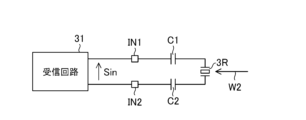
- FIG. 21 is a diagram showing how a reception-only piezoelectric element is connected to a reception circuit according to a sixth example belonging to the embodiment of the present disclosure.
- IC is an abbreviation for integrated circuit.
- the ground refers to a reference conductive portion having a reference potential of 0V (zero volts), or refers to the 0V potential itself.
- the reference conductive part may be formed using a conductor such as metal.
- the potential of 0V is sometimes referred to as a ground potential.
- voltages shown without particular reference represent potentials as seen from ground.
- Level refers to the level of potential, and for any signal or voltage of interest, a high level has a higher potential than a low level.
- a signal or voltage being at a high level strictly means that the level of the signal or voltage is at a high level, and a signal or voltage being at a low level does not strictly mean that the level of the signal or voltage is at a high level. It means that the signal or voltage level is at low level.
- the level of a signal may be expressed as a signal level, and the level of a voltage may be expressed as a voltage level.
- Connections between multiple parts forming a circuit such as arbitrary circuit elements, wiring, nodes, etc., may be understood to refer to electrical connections, unless otherwise specified.
- FIG. 1 shows the overall configuration of an ultrasonic sensor 1 according to an embodiment of the present disclosure.
- the ultrasonic sensor 1 includes a piezoelectric element control IC2 (hereinafter referred to as IC2), a piezoelectric element 3, a transformer TR, a resistor RT , and capacitors CT , C1, and C2.
- IC2 is an example of a piezoelectric element processing device (or piezoelectric element control device).
- the IC 2 includes a transmitting circuit 10 , a receiving processing block 30 including a receiving circuit 31 , and a control circuit 50 .
- a ceramic vibrator ceramic piezoelectric element formed of ceramic can be used as the piezoelectric element 3, other types of piezoelectric elements may also be used.
- FIG. 2 is an external perspective view of the IC2.
- the IC2 includes a semiconductor chip having a semiconductor integrated circuit formed on a semiconductor substrate, a housing (package) that houses the semiconductor chip, and a plurality of external terminals exposed from the housing to the outside of the IC2. It is an electronic component.
- the IC 2 is formed by encapsulating a semiconductor chip in a housing (package) made of resin. Note that the number of external terminals of the IC 2 and the type of the casing of the IC 2 shown in FIG. 2 are merely examples, and they can be designed arbitrarily. FIG.
- FIG. 1 shows a power supply terminal PW, a ground terminal PGND, an output terminal DRV1, an output terminal DRV2, an input terminal IN1, an input terminal IN2, and a communication terminal CM, which are included in the plurality of external terminals. External terminals other than these are also provided on the IC2.
- Power supply voltage VCC is supplied to power supply terminal PW. Each circuit within IC2 is driven based on power supply voltage VCC. Power supply voltage VCC has a predetermined positive DC voltage value. An internal power supply circuit (not shown) that generates another internal power supply voltage from the power supply voltage VCC may be provided within the IC2. A ground terminal PGND is connected to ground.
- the transformer TR has a primary coil L1 and a secondary coil L2, and the primary coil L1 and the secondary coil L2 are magnetically coupled to each other while being electrically insulated from each other.
- a first end of the primary coil L1 is connected to an output terminal DRV1, and a second end of the primary coil L1 is connected to an output terminal DRV2.
- the power supply terminal PW is connected to the middle point (center tap) of the primary coil L1 via a resistor R0. More specifically, the power supply terminal PW is connected to one end of the resistor R0, and the other end of the resistor R0 is connected to the midpoint of the primary coil L1 and to the ground via the capacitor C0.
- a piezoelectric element 3 is connected in parallel to the secondary coil L2. That is, the first end of the secondary coil L2 is connected to the first end of the piezoelectric element 3, and the second end of the secondary coil L2 is connected to the second end of the piezoelectric element 3 and to the ground. . Further, a capacitor C T and a resistor R T are connected in parallel to the secondary coil L2. Furthermore, the first end of the secondary coil L2 and the first end of the piezoelectric element 3 are connected to the input terminal IN1 via the capacitor C1. That is, the first end of the secondary coil L2 and the first end of the piezoelectric element 3 are connected to the first end of the capacitor C1, and the second end of the capacitor C1 is connected to the input terminal IN1.
- the second end of the secondary coil L2 and the second end of the piezoelectric element 3 are connected to the input terminal IN2 via a capacitor C2. That is, the second end of the secondary coil L2 and the second end of the piezoelectric element 3 are connected to the first end of the capacitor C2, and the second end of the capacitor C2 is connected to the input terminal IN2. Note that the capacitors C1 and C2 may be built into the IC2.
- the ultrasonic sensor 1 uses the piezoelectric element 3 to transmit a transmission wave signal W1 in the ultrasonic band toward the external space of the ultrasonic sensor 1 (in a direction away from the ultrasonic sensor 1).
- a reflected wave signal W2 is generated by the transmitted wave signal W1 being reflected by the detection target object OBJ.
- the reflected wave signal W2 is received by the ultrasonic sensor 1 using the piezoelectric element 3.
- the ultrasonic band refers to a frequency band that is higher than the band of sound waves audible to the human ear and is inaudible to the human ear, and generally refers to a band of 20 kHz or higher.
- the transmitted wave signal W1 has a frequency within the range of 30kHz to 80kHz. Both the transmitted wave signal W1 and the reflected wave signal W2 belong to ultrasonic signals.
- the piezoelectric element 3 generates mechanical displacement (vibration) in itself according to a voltage signal applied between its first and second ends, and generates a transmission wave signal W1 by its mechanical displacement. Therefore, the piezoelectric element 3 functions as a transmitter for the transmission wave signal W1. Furthermore, the piezoelectric element 3 has a characteristic of generating an electromotive force between the first end and the second end in response to mechanical displacement (vibration) applied thereto, and also functions as a receiver for the reflected wave signal W2.
- the IC2 uses the piezoelectric element 3 to perform a transmission operation of the transmission wave signal W1 and a reception operation of the reflected wave signal W2.
- a transmission/reception operation the combination of the transmission operation of the transmission wave signal W1 and the reception operation of the reflected wave signal W2 may be referred to as a transmission/reception operation.
- the transmitting circuit 10 is connected to output terminals DRV1 and DRV2.
- the transmitting circuit 10 performs a transmitting operation of the transmitting wave signal W1 under the control of the control circuit 50.
- the transmission circuit 10 drives the piezoelectric element 3 by supplying an alternating current drive current to the primary coil L1. More specifically, in the transmission operation of the transmission wave signal W1, the transmission circuit 10 applies an AC voltage to the secondary coil L2 by supplying an AC drive current to the primary coil L1 via the output terminals DRV1 and DRV2. to occur.
- the receiving circuit 31 is connected to the input terminals IN1 and IN2, and performs a receiving operation of the reflected wave signal W2.
- the receiving circuit 31 uses the piezoelectric element 3 to receive the reflected wave signal W2 in the ultrasonic band. That is, the receiving circuit 31 receives the reflected wave signal W2 by receiving the voltage signal applied across the piezoelectric element 3 via the capacitors C1 and C2.
- the capacitors C1 and C2 remove the DC component of the voltage signal applied across the piezoelectric element 3, and only the AC component of the voltage signal applied across the piezoelectric element 3 is input to the receiving circuit 31 as the input signal Sin.
- the input signal Sin corresponds to the received signal of the reflected wave signal W2 by the receiving circuit 31.
- the input signal Sin also includes a voltage signal applied between both ends of the piezoelectric element 3 during the transmission operation of the transmitted wave signal W1.
- the reception processing block 30 performs necessary signal processing on the reflected wave signal W2 received by the reception circuit 31. Details of the reception processing block 30 will be described later. Note that the operation of each component of the reception processing block 30 is controlled by a control circuit 50.
- the ultrasonic sonar system shown in FIG. 4 can be formed.
- the ultrasonic sonar system in FIG. 4 includes a sensor module 5 formed by modularizing each component of the ultrasonic sensor 1, and an upper device 4.
- the ultrasonic sensor 1 is housed in the sensor module 5.
- a connector 6 connected to the ultrasonic sensor 1 within the sensor module 5 is provided in the sensor module 5 .
- the upper device 4 and the connector 6 are connected to each other via a harness 7.
- the harness 7 includes at least a power supply wiring to which a power supply voltage VCC is applied, a ground wiring to which a ground potential is applied, and a communication wiring.
- a power supply voltage VCC is supplied from the host device 4 to the ultrasonic sensor 1 (IC2) through power supply wiring.
- the communication wiring is connected to the host device 4 and also to the communication terminal CM of the IC 2 via the connector 6.
- the IC 2 and the higher-level device 4 perform bidirectional communication via the communication terminal CM and the communication wiring with reference to the ground potential. Communication between the IC2 and the higher-level device 4 is half-duplex communication, with the higher-level device 4 functioning as a master device and the IC2 functioning as a slave device. Any commands shown below are transmitted from the higher-level device 4 to the IC 2 via the communication wiring and received at the communication terminal CM. Furthermore, in the following description, any signal output (transmitted) from the IC 2 to the higher-level device 4 is input to the higher-level device 4 via the communication terminal CM and the communication wiring.
- the control circuit 50 executes a measurement operation when a predetermined measurement start condition is met.
- the upper-level device 4 can send a measurement instruction command to the IC 2.
- the measurement instruction command is received by the IC 2, the measurement start condition is established, and the control circuit 50 executes the measurement operation.
- a measurement operation is performed only once in response to reception of one measurement instruction command. However, the measurement operation may be repeated multiple times in response to reception of one measurement instruction command.
- the states of the upper-level device 4 and the IC 2 include a first communication state and a second communication state.
- the first communication state is a state in which the host device 4 functions as a transmitting device and the IC2 functions as a receiving device.
- a signal is sent from the host device 4 to the IC 2 via the communication wiring and the communication terminal CM. is sent.
- the second communication state is a state in which the host device 4 functions as a receiving device and the IC2 functions as a transmitting device.
- a signal is sent from the IC 2 to the host device 4 via the communication wiring and the communication terminal CM. is sent.
- the state of the upper-level device 4 and the IC 2 is the first communication state.
- the state of the host device 4 and the IC2 becomes the second communication state only during the execution period of the measurement operation, and returns to the first communication state when the measurement operation is completed.
- each measurement operation after the transmission operation of the transmitted wave signal W1 is performed, the reception operation of the reflected wave signal W2 is performed.
- the length of the execution period of the measurement operation is longer than the length of the execution period of the transmission operation. The length of the execution period of the measurement operation and the length of the execution period of the transmission operation are determined in advance prior to execution of the measurement operation.
- FIG. 6 is a diagram showing transmission and reception operations by the ultrasonic sensor 1.
- the control circuit 50 causes the transmission circuit 10 to perform a transmission operation of the transmission wave signal W1, and can transmit a signal 610 obtained by the reception operation of the reflected wave signal W2 to the upper-level device 4 in response to the transmission operation.
- the signal 610 is a binary signal having a high or low signal level, and corresponds to a signal S35 or S36 described later (see FIG. 8).
- a reception strength signal (corresponding to a reception strength signal S33 to be described later) having a signal value proportional to the strength (amplitude) of the input signal Sin is generated.
- the signal 610 has a high level, and if the value of the reception strength signal is equal to or greater than the determination threshold, the signal 610 has a low level.
- the upper-level device 4 can perform object detection processing based on the signal 610. Note that the proportionality constant between the intensity of the input signal Sin and the received intensity signal may change depending on the elapsed time from the transmission start time of the transmission wave signal W1.
- the object detection process may be a distance detection process that detects the distance between the ultrasonic sensor 1 and the detection target OBJ (in other words, the distance between the piezoelectric element 3 and the detection target OBJ).
- the ultrasonic sensor 1 and the detection target object OBJ can be derived.
- Time t1 represents the start time of transmission of the transmission wave signal W1 using the transmitter circuit 10 and piezoelectric element 3
- time t3 represents the start time of reception of the reflected wave signal W2 using the receiver circuit 31 and piezoelectric element 3.
- Time t2 represents the end time of transmission of the transmission wave signal W1 using the transmission circuit 10 and the piezoelectric element 3.
- Time t2 is a time before time t3.
- signal 610 Before time t1, signal 610 has a high level. Since an AC voltage with a sufficiently large amplitude is applied to the piezoelectric element 3 between times t1 and t2, the signal 610 becomes a low level, and returns to a high level after time t2. Thereafter, the reflected wave signal W2 from the object detection unit OBJ is received at time t3, thereby switching the signal 610 from high level to low level.
- the signal 610 is maintained at a low level, and the signal 610 switches from low level to high level at time t4.
- the length between times t3 and t4 is ideally equal to the length between times t1 and t2.
- the object detection process may be an approach detection process.
- the host device 4 receives the reflected wave signal W2 before a predetermined time elapses after transmitting the transmitted wave signal W1 at time t1, the host device 4 determines that the ultrasonic sensor 1 is a detection target. It is determined that the object OBJ is approaching, and if not, it is determined that the detection target object OBJ is not approaching the ultrasonic sensor 1.
- time t2 if the signal 610 switches from a high level to a low level within a predetermined time from time t1, the host device 4 detects that the object to be detected OBJ approaches the ultrasonic sensor 1. If not, it can be determined that the object to be detected OBJ is not approaching the ultrasonic sensor 1.
- the ultrasonic sensor 1 is mounted on any device.
- a device equipped with the ultrasonic sensor 1 will be referred to as a sensor-equipped device.
- An ultrasonic sonar system (see FIG. 4) having an upper-level device 4 and a sensor module 5 may be installed in a sensor-equipped device.
- a typical example of a sensor-equipped device is a vehicle such as an automobile. It can also be said that the distance between the ultrasonic sensor 1 and the detection target OBJ corresponds to the distance between the sensor mounting device and the detection target OBJ. It can also be said that the approach of the detection target OBJ to the ultrasonic sensor 1 corresponds to the approach of the detection target OBJ to the sensor mounting device.
- the piezoelectric element 3 continues to vibrate for a while based on the mechanical energy accumulated during the supply period of the drive current.
- the vibration of the piezoelectric element 3 after the supply of drive current is stopped is called reverberation. If the duration of reverberation is long, it becomes difficult to detect objects at close range.
- a capacitor C T and a resistor R T are provided to reduce reverberation.
- a resistor was inserted between the capacitor C1 and the input terminal IN1
- a resistor was inserted between the capacitor C2 and the input terminal IN2
- a resistor was inserted between the input terminals IN1 and IN2. It is good that a capacitor is inserted.
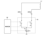
- FIG. 7 shows the internal configuration of the transmitting circuit 10 and the relationship between the transmitting circuit 10 and the control circuit 50.
- the transmitting circuit 10 includes switching elements 11 and 12 and a current source 13.
- a first end (first electrode) of the switching element 11 is connected to the output terminal DRV1, and therefore connected to the first end of the primary coil L1.
- a second end (second electrode) of the switching element 11 is connected to an input end of the current source 13.
- the first end (first electrode) of the switching element 12 is connected to the output terminal DRV2, and therefore connected to the second end of the primary coil L1.
- a second end (second electrode) of the switching element 12 is connected to an input end of the current source 13.
- the current source 13 is a constant current source having an input end and an output end, and operates so that the drive current I DRV flows from its own input end to its own output end.
- the output end of current source 13 is connected to ground.
- the drive current I DRV flows from the input end of the current source 13 toward the output end (therefore, the ground).
- the control circuit 50 can individually control the on and off states of the switching elements 11 and 12. In the transmission operation of the transmission wave signal W1, the control circuit 50 supplies an alternating current drive current to the primary coil L1 by alternately turning on and off the switching elements 11 and 12. More specifically, in the transmission operation, the control circuit 50 alternately switches the state of the transmission circuit 10 between the first drive state and the second drive state.
- switching elements 11 and 12 are on and off, respectively. Therefore, in the first drive state, the first end of the primary coil L1 is electrically connected to the current source 13 through the output terminal DRV1 and the switching element 11, and due to the action of the current source 13, the first end of the primary coil L1 is connected to the output terminal.
- a drive current I DRV flows toward the current source 13 through the DRV 1 and the switching element 11 . Note that the drive current I DRV in the first drive state flows through an electric path passing through the capacitor C0, the center tap of the primary coil L1, and the first end of the primary coil L1 (see also FIG. 1).
- switching elements 11 and 12 are off and on, respectively. Therefore, in the second drive state, the second end of the primary coil L1 is electrically connected to the current source 13 through the output terminal DRV2 and the switching element 12, and due to the action of the current source 13, the second end of the primary coil L1 is connected to the output terminal.
- a drive current I DRV flows toward the current source 13 through the DRV 2 and the switching element 12 .
- the drive current I DRV in the second drive state flows through an electric path passing through the capacitor C0, the center tap of the primary coil L1, and the second end of the primary coil L1 (see also FIG. 1).
- Each of the switching elements 11 and 12 is constituted by, for example, a P-channel type MOSFET (metal-oxide-semiconductor field-effect transistor).
- the sources of the switching elements 11 and 12 may be connected to the output terminals DRV1 and DRV2, respectively, while the drains of the switching elements 11 and 12 may be connected to the input terminal of the current source 13.
- the control circuit 50 may individually control the on/off states of the switching elements 11 and 12 by controlling the gate potentials of the switching elements 11 and 12.
- the switching elements 11 and 12 may be configured with N-channel MOSFETs.
- the current source 13 may be a variable current source configured to be able to change the value of the drive current I DRV , and the control circuit 50 may be able to adjust the value of the drive current I DRV .
- FIG. 8 shows an internal block diagram of the reception processing block 30.
- the reception processing block 30 includes a reception circuit 31, an ADC 32, a signal processing circuit 33, a comparison signal generation circuit 34, a comparison circuit 35, a filter circuit 36, a signal selection circuit 37, a DAC 38, a switching output circuit 39, and a selection designation circuit 40. .
- the operations of the components (31 to 40) of the reception processing block 30 are controlled by a control circuit 50.
- the receiving circuit 31 is connected to the input terminals IN1 and IN2 as described above.
- a signal between input terminals IN1 and IN2 indicates an alternating current component of a voltage signal applied between both ends of piezoelectric element 3, and is input to receiving circuit 31 as input signal Sin.
- the receiving circuit 31 performs a signal amplification process to amplify the input signal Sin, and generates and outputs the amplified input signal Sin as an amplified received signal S31.
- the amplified received signal S31 is an analog signal having an amplitude proportional to the amplitude of the input signal Sin.
- the amplified received signal S31 is input to the ADC 32.
- the ADC 32 is an A/D converter (analog/digital converter), and generates and outputs a signal S32 by converting the amplified received signal S31 into a digital signal. Since the signal S32 is a signal obtained by converting the amplified received signal S31 expressed in the analog domain into a signal expressed in the digital domain, the signal S32 can also be referred to as an amplified received signal.
- the digital amplified reception signal S32 is input to the signal processing circuit 33.
- the signal processing circuit 33 generates and outputs a reception strength signal S33 by performing predetermined signal processing on the amplified reception signal S32.
- the reception strength signal S33 is a signal indicating the strength of the input signal Sin (that is, a signal indicating the strength of the reception signal at the reception circuit 31).
- the reception strength signal S33 is a digital signal (signal in the digital domain), and the greater the strength of the input signal Sin at a certain time, the greater the value of the reception strength signal S33 at that time.
- the signal processing in the signal processing circuit 33 includes envelope detection for detecting the envelope of the amplified received signal S32.
- the intensity (amplitude) of the input signal Sin can be specified by detecting the envelope of the amplified received signal S32.
- the signal processing in the signal processing circuit 33 may further include processing other than envelope detection (for example, digital filtering). Note that the content of the signal processing in the signal processing circuit 33 is arbitrary as long as a signal indicating the strength of the input signal Sin (that is, a signal indicating the strength of the received signal at the receiving circuit 31) can be generated as the reception strength signal S33.
- the signal processing circuit 33 is an example of a reception strength signal generation circuit. It may be considered that the ADC 32 and the signal processing circuit 33 form a reception strength signal generation circuit.
- the comparison signal generation circuit 34 generates and outputs a comparison signal S34, which is a signal to be compared with the reception strength signal S33.
- the comparison signal S34 is a digital signal (signal in the digital domain), and the value of the comparison signal S34 is sometimes particularly referred to as a determination threshold value.
- the determination threshold value that is, the value of the comparison signal S34 changes with the passage of time from the transmission start time of the transmission wave signal W1.
- the reception strength signal S33 and comparison signal S34 are input to the comparison circuit 35.
- Comparison circuit 35 compares reception strength signal S33 and comparison signal S34, and outputs signal S35 indicating the comparison result.
- Signal S35 and signal S36 which will be described later, are binary signals having a value of "1" or "0". Here, it is assumed that the "1" signals S35 and S36 have a low level, and the "0" signals S35 and S36 have a high level.
- the comparison circuit 35 outputs a signal S35 of "1” if the value of the reception strength signal S33 is equal to or greater than the value of the comparison signal S34, and outputs a signal S35 of "1” if the value of the reception strength signal S33 is less than the value of the comparison signal S34.
- a signal S35 of 0'' is output. Signals S35 and S36 may especially be referred to as comparison result signals.
- the comparison result signal S35 is input to the filter circuit 36.
- the filter circuit 36 performs filtering processing on the comparison result signal S35 with the main purpose of reducing noise contained in the comparison result signal S35, and outputs the comparison result signal S35 after the filtering process as a comparison result signal S36. Note that in the reception processing block 30, the function of the filter circuit 36 may be disabled or the filter circuit 36 may not be provided. In that case, the comparison result signal S36 indicates exactly the same thing as the comparison result signal S35.
- a reception strength signal S33 and a comparison signal S34 are input to the signal selection circuit 37.
- the selection designation signal S40 from the selection designation circuit 40 is also input to the signal selection circuit 37.
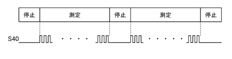
- the selection designation signal S40 is a binary signal having a value of "1" or "0".
- the signal selection circuit 37 selects either the reception strength signal S33 or the comparison signal S34 in response to the selection designation signal S40, and outputs the selected signal as the signal S37.
- the selection designation signal S40 has a value of "1”
- the reception strength signal S33 is selected as the signal S37
- the comparison signal S34 is selected as the signal S37. shall be selected as.
- Signal S37 may hereinafter be referred to as selection signal S37.
- the selection signal S37 is input to the DAC38.
- the DAC 38 is a D/A converter (digital/analog converter), and generates and outputs a signal S38 by converting the selection signal S37 into an analog signal.
- Signal S38 may hereinafter be referred to as DAC output signal S38.
- the analog DAC output signal S38 is input to the switching output circuit 39.
- the switching output circuit 39 outputs either the comparison result signal S36 or the DAC output signal S38 from the communication terminal CM as the IC output signal S39 under the control of the control circuit 50.
- the IC output signal S39 output from the communication terminal CM is transmitted to the host device 4 via the communication wiring.
- a signal output circuit 41 is formed by the signal selection circuit 37, DAC 38, switching output circuit 39, and selection designation circuit 40.
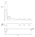
- FIG. 9 shows waveform examples of signals S33, S34, and S35 in one measurement operation.
- the reception strength signal S33 is shown by a broken line waveform
- the comparison signal S34 and comparison result signal S35 are shown by a solid line waveform. If noise and the like are ignored, the waveforms of the comparison result signal S35 and the comparison result signal S36 shown in FIG. 9 are substantially the same.
- One measurement operation starts at time t1 and ends at time t10.
- the control circuit 50 executes the measurement operation using the transmitting circuit 10 and the components (31 to 40) of the receiving processing block 30. It may be considered that under the control of the control circuit 50, the transmitting circuit 10 and the components (31 to 40) of the receiving processing block 30 cooperate to execute the measurement operation.
- Time t2 is a time before time t10, which corresponds to the end time of the execution period of the measurement operation.
- a transmission wave signal W1 is transmitted from the piezoelectric element 3 between times t1 and t2. Transmission of the transmission wave signal W1 is stopped at time t2.
- times t1 and t2 described here correspond to times t1 and t2 described above with reference to FIG. 6, and times t3 and t4 described above are times before time t10.
- the length of the execution period of the transmission operation is the transmission setting time T O corresponding to the length between times t1 and t2, and the length of the execution period of the measurement operation is the measurement setting time corresponding to the length between times t1 and t10.
- the time is T M.
- the transmission set time T O and the measurement set time T M are determined in advance prior to execution of the measurement operation. It may be considered that the control circuit 50 sets the transmission set time T O and the measurement set time T M.
- the transmission setting time T O and the measurement setting time T M can be changed based on a setting command transmitted from the upper-level device 4 and received by the IC 2.
- the comparison result signal S35 becomes a low level, and returns to a high level after time t2. Thereafter, the comparison result signal S35 becomes low level only during the period in which the value of the reception strength signal S33 is greater than or equal to the value of the comparison signal S34.
- the comparison signal generation circuit 34 sets the determination threshold (that is, the value of the comparison signal S34) to the transmission start time of the transmission wave signal W1. It changes with the passage of time from t1. For example, when the ultrasonic sonar system is mounted on a vehicle that runs on a road surface, the road surface is excluded from the detection target object OBJ. At this time, in order to avoid erroneously detecting the road surface as the detection target object OBJ based on the reflected waves from the road surface, the determination threshold value is set relatively in the time period when the reflected waves from the road surface are received by the receiving circuit 31. Things like raising the price are done. Further, the comparison signal S34 is set in consideration of the fact that as the distance between the detection target object OBJ and the ultrasonic sensor 1 increases, the intensity of the reflected wave signal W2 received by the receiving circuit 31 decreases.
- determination threshold data that specifies how to change the value of the comparison signal S34 from time t1 to time t10 is stored in the control circuit 50 or the comparison signal generation circuit 34, and the comparison signal generation circuit 34
- the circuit 34 may generate and output the comparison signal S34 based on the determination threshold data.
- the determination threshold data may be changed based on a setting command transmitted from the upper-level device 4 and received by the IC 2.
- the comparison signal generation circuit 34 may change the determination threshold depending on the gain of signal amplification in the reception circuit 31 or the signal processing circuit 33.
- the signal output circuit 41 operates in one of a plurality of output modes.
- the control circuit 50 designates and controls which output mode the signal output circuit 41 operates in.
- the control circuit 50 sets any one of the plurality of output modes to the target output mode according to the mode designation command received from the host device 4, and the signal output circuit 41 operates in the target output mode.
- the plurality of output modes include output modes MD A and MD B.
- the output mode MD A will be explained.
- the target output mode is output mode MD A.
- the output mode MD A is used in the actual operation stage where the ultrasonic sonar system is mounted on a sensor-equipped device (such as a vehicle) and object detection processing is performed.
- the output mode MD A is used in the actual operation stage where the ultrasonic sonar system is mounted on a sensor-equipped device (such as a vehicle) and object detection processing is performed.
- the output mode MD A that is, when the output mode MD A is set to the target output mode
- the comparison result signal S36 is sent to the communication terminal as the IC output signal S39 throughout the execution period of the measurement operation. Output from CM.
- the signal output circuit 41 operates as a comparison circuit from the transmission start time (t1) of the transmission wave signal W1 until the measurement set time T M elapses (that is, until the measurement operation ends).
- a signal based on the comparison result of No. 35 is output from the communication terminal CM.
- the host device 4 can perform the above-described object detection process based on the IC output signal S39 in the output mode MD A.
- the control circuit 50 operates the signal selection circuit 37, DAC 38, and selection designation circuit 40 during a period in which the DAC output signal S38 is output as the IC output signal S39, and operates the signal selection circuit 37, DAC 38, and selection designation circuit 40 in other periods.
- the operation of the circuit 40 is stopped. Therefore, in the output mode MD A (that is, when the output mode MD A is set to the target output mode), the control circuit 50 stops the operations of the signal selection circuit 37, DAC 38, and selection designation circuit 40.
- the switching output circuit 39 may have a configuration as shown in FIG.
- the switching output circuit 39 in FIG. 10 has an I/F circuit 39a.
- the comparison result signal S36 is input to the input terminal of the I/F circuit 39a.
- An output terminal of the I/F circuit 39a is connected to a communication terminal CM.
- the I/F circuit 39a operates effectively during the period in which the comparison result signal S36 is to be output as the IC output signal S39, and outputs the comparison result signal S36 as the IC output signal S39 from the communication terminal CM during this period. At this time, necessary level shift processing and the like are executed as appropriate.
- the output terminal of the DAC 38 is connected to the communication terminal CM together with the output terminal of the I/F circuit 39a. However, when the operation of the DAC 38 is stopped, the input impedance of the output terminal of the DAC 38 is sufficiently high when viewed from the communication terminal CM. Therefore, in the measurement operation in the output mode MD A , the IC output signal S39 corresponding to the comparison result signal S36 can be output from the communication terminal CM through the I/F circuit 39a.
- the DAC output signal S38 can be output from the communication terminal CM as the IC output signal S39.
- debugging work work including adjustment of determination thresholds and the like (hereinafter referred to as debugging work) is performed.
- the worker responsible for the debugging work desires to refer to various internal signals within the IC2.
- the IC 2 has the configuration and output mode MD B shown in FIG. 8.
- some reference configurations are shown below.
- the components 37 to 40 shown in FIG. 8 are not provided, and only the comparison result signal S36 can be output from the communication terminal CM.
- a wiring WR is drawn out from the IC exclusively for debugging work, and a signal on the wiring WR (for example, a signal at S33 or S34) is observed using a special jig or the like. do.
- a step of drawing out the wiring WR from the IC exclusively for debugging is required, which is inconvenient.
- the components 37 and 40 shown in FIG. 8 are not provided.
- the comparison result signal S36 or the reception strength signal S33 can be switched and output from the communication terminal CM. Therefore, during debugging work related to the second reference configuration, the operator can easily observe the reception strength signal S33. However, in the second reference configuration, only the reception strength signal S33 can be observed during debugging, making it difficult to proceed with the debugging.
- Output mode MD B The configuration and output mode MD B shown in FIG. 8 facilitate debugging work.
- the signal output circuit 41 outputs m types of output target signals from the communication terminal CM while switching them.
- m is an arbitrary integer of 2 or more.
- the m types of output target signals are composed of output target signals S[1] to S[m].
- any two mutually different natural numbers less than or equal to m are represented by i A and i B.
- the output target signal S[i A ] is a signal representing the waveform of the reception strength signal S33
- the output target signal S[i B ] is a signal representing the waveform of the comparison signal S34. That is, any two of the output target signals S[1] to S[m] are a signal representing the waveform of the reception strength signal S33 and a signal representing the waveform of the comparison signal S34.
- the output target signal S[i A ] is the DAC output signal S38 when the reception strength signal S33 is the selection signal S37, that is, the reception strength signal S33 is converted into an analog signal.
- the output target signal S[i A ] may be any signal that represents the waveform of the reception strength signal S33.
- the output target signal S[i B ] is the DAC output signal S38 when the comparison signal S34 is the selection signal S37, that is, the comparison signal S34 is converted into an analog signal.
- the output target signal S[i B ] may be any signal that represents the waveform of the comparison signal S34.
- a debugging worker can easily observe the waveform of the received strength signal S33 and the waveform of the comparison signal S34 based on the signal output from the communication terminal CM, and make a decision. Debugging work including threshold adjustment etc. can be performed efficiently.
- output mode MD B is output mode MD B1 .
- "m 2"
- the signal output circuit 41 outputs the output target signal from the transmission start time (t1) of the transmission wave signal W1 until the measurement set time T M elapses (that is, until the measurement operation ends).
- S[1] and S[2] are sequentially switched and output from the communication terminal CM.
- Outputting from the communication terminal CM while sequentially switching the output target signals S[1] and S[2] means, in other words, outputting from the communication terminal CM while switching the output target signals S[1] and S[2] alternately. It corresponds to doing.
- the switching period of the signal output from the communication terminal CM in the output mode MD B1 is represented by the symbol "P SW ".
- the signal output from the communication terminal CM is switched between the output target signals S[1] and S[2] every time the switching period P SW elapses.
- the switching period P SW is sufficiently shorter than the measurement setting time T M . Therefore, in the measurement operation related to the output mode MD B1 , the signal output circuit 41 outputs the output target signals S[1] and S[ with a cycle shorter than the measurement setting time T M (that is, a cycle shorter than the execution period of the measurement operation). 2] is output from the communication terminal CM while being switched periodically (alternately).
- the sensor driving frequency is 50 to 60 kHz (kilohertz).
- the sensor drive frequency represents the frequency of the AC voltage applied to the piezoelectric element 3 during the transmission operation of the transmission wave signal W1, and in the configuration of FIG. 1, is equal to the frequency of the AC current supplied to the primary coil L1.
- the reciprocal of the sensor drive frequency is called the sensor drive period.
- the switching period P SW may be about several tens of microseconds.
- the update period of any digital signal in the reception processing block 30 may match the sensor drive period, and in this case, for example, the switching period P SW may be 1/2 of the sensor drive period (however, 1/2 is just an example and can be modified in various ways).
- FIG. 14 schematically shows the waveform of the IC output signal S39 during the execution period of the measurement operation related to the output mode MD B1 .
- waveforms 711 and 712 are shown on the display screen of the oscilloscope.
- the waveform 711 is shown as a broken line waveform
- the waveform 712 is shown as a solid line waveform.
- the waveform 711 is the waveform of the output target signal S[1], and thus represents the waveform of the reception strength signal S33.
- the waveform 712 is the waveform of the output target signal S[2], and thus represents the waveform of the comparison signal S34.
- FIG. 15 is an enlarged view (enlarged view in the time direction) of waveforms 711 and 712 around time t2. It can be seen that the IC output signal S39 is switched between the output target signals S[1] and S[2] every time the switching period P SW elapses. Since the switching period P SW is sufficiently short with respect to the measurement setting time T M , when the waveform of the IC output signal S39 is observed with an oscilloscope on the entire scale of the measurement setting time T M , the waveforms 711 and 712 are overlapped. observed at the same time. That is, the debugging worker can simultaneously observe the waveform of the reception strength signal S33 and the comparison signal S34, and can efficiently perform the debugging work.
- FIG. 16 shows the waveform of the selection designation signal S40 in the output mode MD B1 .
- the value of the selection designation signal S40 alternately changes between “1” and “0” every time the switching period P SW elapses.
- the selection signal S37 is the reception strength signal S33 when the selection designation signal S40 has a value of "1”, and is the comparison signal S34 when the selection designation signal S40 has a value of "0".
- the value of the selection designation signal S40 during the non-execution period of the measurement operation is arbitrary, but in the example of FIG. 16, it is fixed at "0".
- output mode MD B is output mode MD B2 .
- "m 2"
- the output target signals S[1] and S[2] are alternately switched and output from the communication terminal CM during each measurement operation.
- the signal output from the communication terminal CM is switched between the output target signals S[1] and S[2] every time one measurement operation is performed. .
- the signal output circuit 41 operates from the transmission start time (t1) of the transmission wave signal W1 until the measurement set time T M has elapsed (that is, until the measurement operation ends). , outputs only one of the output target signals S[1] and S[2] from the communication terminal CM.
- the signal output circuit 41 outputs the signal output from the communication terminal CM to the output target signals S[1] and S every time one measurement operation is executed. [2] Switch alternately between.
- FIG. 17 schematically shows the waveform of the IC output signal S39 in the output mode MD B2 .
- the i-th measurement operation is performed between times t21 and t22, then the (i+1)-th measurement operation is performed between times t23 and t24, and further thereafter, the i-th measurement operation is performed between times t25 and t24.
- the (i+2)th measurement operation is performed between times t26 and then the (i+3)th measurement operation is performed between times t27 and t28.
- i is any natural number.
- the signal output circuit 41 outputs the output target signal S[1] from the communication terminal CM in the i-th measurement operation, and outputs the output target signal S[2] from the communication terminal CM in the (i+1)th measurement operation. Then, in the (i+2)th measurement operation, the output target signal S[1] is output from the communication terminal CM, and in the (i+3)th measurement operation, the output target signal S[2] is output from the communication terminal CM.
- the waveform of the IC output signal S39 in FIG. 17 is a waveform 721 between times t21 and t22, a waveform 722 between times t23 and t24, a waveform 723 between times t25 and t26, and a waveform 724 between times t27 and t28. ,including.
- the waveform 721 is the waveform of the output target signal S[1] between times t21 and t22, and therefore represents the waveform of the reception strength signal S33 between times t21 and t22.
- the waveform 722 is the waveform of the output target signal S[2] between times t23 and t24, and therefore represents the waveform of the comparison signal S34 between times t23 and t24.
- the waveform 723 is the waveform of the output target signal S[1] between times t25 and t26, and therefore represents the waveform of the reception strength signal S33 between times t25 and t26.
- the waveform 724 is the waveform of the output target signal S[2] between times t27 and t28, and therefore represents the waveform of the comparison signal S34 between times t27 and t27.
- a waveform in which waveforms 721 to 724 are arranged along the time axis direction as shown in FIG. 17 is observed.
- Many oscilloscopes are equipped with an afterimage display function that displays a waveform once displayed on the display screen as an afterimage.
- the afterimage display function waveforms 721' and 722' as shown in FIG. 18 can be displayed in a superimposed manner on the display screen of the oscilloscope.
- a solid line waveform 722' corresponds to the waveform 722 in FIG. 17
- a broken line waveform 721' corresponds to the waveform 721 in FIG.
- the waveform 721' is displayed superimposed on the waveform 722' by the afterimage display function.
- the output mode MD B2 also allows debugging workers to observe the waveform of the reception strength signal S33 and the comparison signal S34, and by using the afterimage display function, etc., these waveforms can be observed simultaneously. You can also do it. Therefore, debugging work can be performed efficiently.
- FIG. 19 shows the waveform of the selection designation signal S40 in the output mode MD B2 .
- the output mode MD B1 according to the first embodiment and the output mode MD B2 according to the second embodiment will be compared.
- the waveforms of the reception strength signal S33 and the comparison signal S34 obtained in the same measurement operation can be observed simultaneously, so there is an advantage that no mismatch occurs between the waveforms.
- CR filters or slew rate control are often applied to signals propagated to communication wiring as a countermeasure against EMI or malfunction.
- the waveform observed as the IC output signal S39 may not correctly represent the waveform of the signal S33 or S34 because the output tracking is not in time due to the need for high-speed switching. . Therefore, set the switching period P SW to be longer, or lower the value of the pull-up resistor connected to the communication wiring (assuming that a method is adopted in which signal transmission is performed depending on whether or not current flows through the pull-up resistor). ) may be necessary.
- the signal switching period is quite long, so there is no concern about output tracking.
- the reception strength signal S33 and the comparison signal S34 observed in the output mode MD B2 are not signals acquired during the same measurement operation, there is a possibility that a mismatch will occur between their waveforms ( (There may be a deviation in the relationship between the determination threshold and the received signal strength.)
- the output mode MD B (ie, the output mode MD B1 ) according to the first embodiment can be modified to suit the condition of "m ⁇ 3".
- the output mode MD B subjected to this modification is referred to as an output mode MD B3 .
- the output mode MD B according to the third embodiment is the output mode MD B3 , and "m ⁇ 3" in the third embodiment. Note that when "m ⁇ 3", the configuration of the signal output circuit 41 may be modified from the configuration shown in FIG. 8 as appropriate.
- the signal output circuit 41 outputs the output target signal from the transmission start time (t1) of the transmission wave signal W1 until the measurement set time T M has elapsed (that is, until the measurement operation ends). Output from the communication terminal CM while sequentially switching S[1] to S[m].
- the signal output from the communication terminal CM is sequentially switched between the output target signals S[1] to S[m] every time the switching period P SW elapses. As described above, the switching period P SW is sufficiently shorter than the measurement setting time T M .
- the signal output circuit 41 outputs the output target signals S[1] to S[ with a cycle shorter than the measurement setting time T M (that is, a cycle shorter than the execution period of the measurement operation). m] is outputted from the communication terminal CM while sequentially switching periodically.
- the signal output from the communication terminal CM changes from the output target signal S[1] to the output target signal S every time the switching period P SW elapses. [m], the output target signals S[1], S[2], S[3]...S[m] are sequentially switched.
- the switching period P SW has elapsed after the output target signal S[m] started being output from the communication terminal CM
- the signal output from the communication terminal CM returns to the output target signal S[1], and the same switching output is performed thereafter. It will be done.
- the output target signal S[1] is a signal representing the waveform of the reception strength signal S33
- the output target signal S[2] is a signal for comparison. This signal represents the waveform of signal S34. Any signal within the IC2 can be set as the output target signals S[3] to S[m].
- a lower limit analog signal representing the lower limit potential of the DAC output signal S38 or an upper limit analog signal representing the upper limit potential of the DAC output signal S38 is set to any of the output target signals S[3] to S[m]. It's good.
- the DAC output signal S38 is an analog signal having a potential from a lower limit signal level (zero scale level) to an upper limit signal level (full scale level). Therefore, in the configuration of FIG. 8, when the DAC output signal S38 becomes the IC output signal S39, the output target signals S[1] to S[m] all have potentials from the lower limit signal level to the upper limit signal level.
- the potential of the upper limit signal level is higher than the potential of the lower limit signal level.
- the waveforms 721 to 724 in FIG. 17, or the waveforms 721' and 722' in FIG. It is difficult to recognize the upper limit signal level (full scale level).
- the waveform of the observation target signal for example, waveforms 711 and 712 in FIG. 14
- the lower limit signal level cannot be clearly recognized, it is possible to determine whether noise is superimposed on the observation target signal and whether the noise is superimposed on the observation target signal. Difficult to grasp the degree etc.
- the waveform of the observation target signal (for example, waveforms 711 and 712 in FIG. 14) is displayed on the display screen of the oscilloscope, and the upper limit signal level cannot be clearly recognized, it is difficult to determine whether the observation target signal has reached the upper limit signal level. or the difference between the level of the signal to be observed and the upper limit signal level.
- the output mode MD B (ie, the output mode MD B2 ) according to the second embodiment can be modified to suit the condition of "m ⁇ 3".
- the output mode MD B subjected to this modification is referred to as an output mode MD B4 .
- the output mode MD B according to the fourth embodiment is the output mode MD B4 , and "m ⁇ 3" in the fourth embodiment. Note that when "m ⁇ 3", the configuration of the signal output circuit 41 may be modified from the configuration shown in FIG. 8 as appropriate.
- the signal output circuit 41 In the measurement operation related to the output mode MD B4 , the signal output circuit 41 outputs the output target signal from the transmission start time (t1) of the transmission wave signal W1 until the measurement set time T M has elapsed (that is, until the measurement operation ends). Any one of S[1] to S[m] is continuously output from the communication terminal CM.
- the signal output circuit 41 When the measurement operation is repeatedly executed multiple times in the output mode MD B4 , the signal output circuit 41 outputs the signal output from the communication terminal CM as the output target signals S[1] to S every time one measurement operation is executed. Switch sequentially between [m].
- the signal output from the communication terminal CM changes from the output target signal S[1] to the output target signal every time one measurement operation is executed.
- the output target signals S[1], S[2], S[3]...S[m] are sequentially switched toward S[m].
- the signal output from the communication terminal CM in the next measurement operation returns to the output target signal S[1]. Thereafter, similar switching output is performed.
- the output target signal S[1] is a signal representing the waveform of the reception strength signal S33
- the output target signal S[2] is a signal for comparison.
- This signal represents the waveform of signal S34.
- Any signal within the IC2 can be set as the output target signals S[3] to S[m].
- the lower limit analog signal or the upper limit analog signal may be set as one output target signal.
- the signal output circuit 41 may operate in any of the first to nth output modes.
- n is an arbitrary integer of 2 or more.
- the output mode MD A is the first output mode.
- it is basically assumed that "n 2", but "n ⁇ 3" may be satisfied.
- any one or more output modes among the above output modes MD B1 , MD B2 , MD B3_1 , MD B3_2 , MD B3_3 , MD B4_1 , MD B4_2 and MD B4_3 are set as the second to nth output modes.
- the output modes MD B1 , MD B2 , MD B3_1 , MD B3_2 , MD B3_3 , MD B4_1 , MD B4_2 and MD B4_3 may be the second to ninth output modes, respectively.
- the control circuit 50 specifies and controls in which output mode the signal output circuit 41 operates.
- the control circuit 50 sets any one of the first to nth output modes to the target output mode in accordance with the mode designation command received from the host device 4, and the signal output circuit 41 operates in the target output mode.
- the single piezoelectric element 3 functions as a transmitter for the transmitted wave signal W1 and as a receiver for the reflected wave signal W2.
- a piezoelectric element 3R as a wave receiver may be separately provided as shown in FIG.
- the piezoelectric element 3 is not connected to the capacitors C1 and C2, but instead the first end of the piezoelectric element 3R is connected to the first end of the capacitor C1, and the second end of the capacitor C1 is connected to the input terminal IN1.
- the piezoelectric element 3R is arranged at a position separated from the piezoelectric element 3, and receives the reflected wave signal W2 to generate a voltage signal between both ends of the piezoelectric element 3R.
- the receiving circuit 31 is connected to the input terminals IN1 and IN2, and performs a receiving operation of the reflected wave signal W2.
- the receiving circuit 31 receives the reflected wave signal W2 in the ultrasonic band using the piezoelectric element 3R. That is, the receiving circuit 31 receives the reflected wave signal W2 by receiving the voltage signal applied across the piezoelectric element 3R via the capacitors C1 and C2.
- the capacitors C1 and C2 remove the DC component of the voltage signal applied across the piezoelectric element 3R, and only the AC component of the voltage signal applied across the piezoelectric element 3R is input to the receiving circuit 31 as the input signal Sin.
- the input signal Sin corresponds to the received signal of the reflected wave signal W2 by the receiving circuit 31. It is as described above except that the piezoelectric element that generates the input signal Sin is the piezoelectric element 3R.
- a configuration in which the transformer TR is not provided in the ultrasonic sensor 1 may be adopted.
- the output terminals DRV1 and DRV2 are directly connected to the first and second ends of the piezoelectric element 3, respectively, and in the transmission operation, the transmitting circuit 10 supplies an AC voltage of a predetermined amplitude between both ends of the piezoelectric element 3.
- the piezoelectric element 3 may be driven by the following.
- the upper-level device 4 is, for example, an ECU (Electronic Control Unit) mounted on the vehicle.
- ECU Electronic Control Unit
- the ECU can perform object detection processing.
- the IC 2 may be operated in the output mode MD B with the ultrasonic sensor 1 connected to the ECU, and in this case, the ECU can be used for debugging.
- a device dedicated to debugging work may be used as the upper-level device 4.
- a piezoelectric element processing device (2) includes a transmitting circuit (10) configured to transmit a transmission wave signal (W1) from the piezoelectric element by driving the piezoelectric element (3). , a receiving circuit (31) configured to receive a reflected wave signal (W2) of the transmitted wave signal by an object using the piezoelectric element or another piezoelectric element (3R); A reception strength signal generation circuit (33) configured to generate a reception strength signal (S33) representing the strength, and a comparison signal (33) whose signal value changes as time elapses from the transmission start time of the transmission wave signal.
- a comparison signal generation circuit (34) configured to generate a signal S34), a comparison circuit (35) configured to compare the reception strength signal and the comparison signal, and a signal generation circuit (35) configured to generate a signal from a communication terminal (CM).
- a signal output circuit (41) configured to be able to output a A first output mode (MD A ) in which a signal is output from the communication terminal, and a second output mode (MD B ), and the plurality of output target signals include a signal representing the waveform of the received strength signal and a signal representing the waveform of the comparison signal, and two output target signals (S[1] and S[2] ) (first configuration).
- a measurement operation is performed using the transmission circuit, the reception circuit, the reception strength signal generation circuit, the comparison signal generation circuit, the comparison circuit, and the signal output circuit.
- the measurement operation includes a transmission operation of causing the transmission circuit to transmit the transmission wave signal for a transmission setting time, and the measurement operation in the first output mode.
- the signal output circuit outputs a signal based on the comparison result of the comparison circuit from the communication terminal, and in the measurement operation in the second output mode, the signal output circuit outputs the plurality of output target signals.
- a configuration (second configuration) may be adopted in which output is output from the communication terminal while sequentially switching.
- the signal output circuit in the measurement operation in the second output mode, the signal output circuit outputs the plurality of outputs at a cycle (P SW ) shorter than the execution period of the measurement operation.
- a configuration (third configuration) may be adopted in which the target signal is outputted from the communication terminal while being periodically and sequentially switched.
- a measurement operation is performed using the transmission circuit, the reception circuit, the reception strength signal generation circuit, the comparison signal generation circuit, the comparison circuit, and the signal output circuit.
- the measurement operation includes a transmission operation of causing the transmission circuit to transmit the transmission wave signal for a transmission setting time, and the measurement operation in the first output mode.
- the signal output circuit outputs a signal based on the comparison result of the comparison circuit from the communication terminal, and in the measurement operation in the second output mode, the signal output circuit outputs a signal based on the comparison result of the comparison circuit, and in the measurement operation in the second output mode, the signal output circuit outputs a signal based on the comparison result of the comparison circuit.
- the signal output circuit When one of the signals is output from the communication terminal and the measurement operation is repeatedly executed a plurality of times in the second output mode, the signal output circuit outputs the signal from the communication terminal each time the measurement operation is executed.
- a configuration (fourth configuration) may be adopted in which the signal to be outputted is sequentially switched among the plurality of output target signals.
- the signal output circuit controls the plurality of signals in the i-th measurement operation. Output any one of the output target signals from the communication terminal, and output any other one of the plurality of output target signals from the communication terminal in the (i+1)th measurement operation.
- i may represent a natural number (fifth configuration).
- each output target signal is an analog signal having a potential from a lower limit signal level to an upper limit signal level
- one of the plurality of output target signals is One of them may be a lower limit analog signal having the lower limit signal level or an upper limit analog signal having the upper limit signal level (sixth configuration).
- An ultrasonic sensor is an ultrasonic sensor including a piezoelectric element processing device according to any one of the first to sixth configurations, and the piezoelectric element, the receiving circuit is a configuration (seventh configuration) in which the reflected wave signal is received using the piezoelectric element.
- An ultrasonic sensor includes the piezoelectric element processing device according to any of the first to sixth configurations, the piezoelectric element, and the other piezoelectric element.
- the receiving circuit is configured to receive the reflected wave signal using the other piezoelectric element (eighth configuration).
Landscapes
- Engineering & Computer Science (AREA)
- Physics & Mathematics (AREA)
- Radar, Positioning & Navigation (AREA)
- Remote Sensing (AREA)
- Computer Networks & Wireless Communication (AREA)
- General Physics & Mathematics (AREA)
- Acoustics & Sound (AREA)
- Measurement Of Velocity Or Position Using Acoustic Or Ultrasonic Waves (AREA)
Priority Applications (1)
| Application Number | Priority Date | Filing Date | Title |
|---|---|---|---|
| JP2024546721A JPWO2024057661A1 (https=) | 2022-09-14 | 2023-06-26 |
Applications Claiming Priority (2)
| Application Number | Priority Date | Filing Date | Title |
|---|---|---|---|
| JP2022-145934 | 2022-09-14 | ||
| JP2022145934 | 2022-09-14 |
Publications (1)
| Publication Number | Publication Date |
|---|---|
| WO2024057661A1 true WO2024057661A1 (ja) | 2024-03-21 |
Family
ID=90274532
Family Applications (1)
| Application Number | Title | Priority Date | Filing Date |
|---|---|---|---|
| PCT/JP2023/023590 Ceased WO2024057661A1 (ja) | 2022-09-14 | 2023-06-26 | 圧電素子用処理装置及び超音波センサ |
Country Status (2)
| Country | Link |
|---|---|
| JP (1) | JPWO2024057661A1 (https=) |
| WO (1) | WO2024057661A1 (https=) |
Citations (4)
| Publication number | Priority date | Publication date | Assignee | Title |
|---|---|---|---|---|
| JPH11160430A (ja) * | 1997-11-25 | 1999-06-18 | Kojima Press Co Ltd | 超音波を用いた障害物検出装置 |
| JP2006343218A (ja) * | 2005-06-09 | 2006-12-21 | Toto Ltd | 超音波人体センサ及びそれを有するトイレ装置 |
| US20080089178A1 (en) * | 2004-08-04 | 2008-04-17 | Thomas Knittel | Ultrasonic Sensor Comprising An Adjustable Detection Area |
| JP2019200194A (ja) * | 2018-05-11 | 2019-11-21 | アイシン精機株式会社 | 物体検知装置および駐車支援装置 |
-
2023
- 2023-06-26 WO PCT/JP2023/023590 patent/WO2024057661A1/ja not_active Ceased
- 2023-06-26 JP JP2024546721A patent/JPWO2024057661A1/ja active Pending
Patent Citations (4)
| Publication number | Priority date | Publication date | Assignee | Title |
|---|---|---|---|---|
| JPH11160430A (ja) * | 1997-11-25 | 1999-06-18 | Kojima Press Co Ltd | 超音波を用いた障害物検出装置 |
| US20080089178A1 (en) * | 2004-08-04 | 2008-04-17 | Thomas Knittel | Ultrasonic Sensor Comprising An Adjustable Detection Area |
| JP2006343218A (ja) * | 2005-06-09 | 2006-12-21 | Toto Ltd | 超音波人体センサ及びそれを有するトイレ装置 |
| JP2019200194A (ja) * | 2018-05-11 | 2019-11-21 | アイシン精機株式会社 | 物体検知装置および駐車支援装置 |
Also Published As
| Publication number | Publication date |
|---|---|
| JPWO2024057661A1 (https=) | 2024-03-21 |
Similar Documents
| Publication | Publication Date | Title |
|---|---|---|
| US6946808B2 (en) | Motor drive control circuit and motor drive apparatus | |
| US10739453B2 (en) | Ultrasonic measuring system, in particular for measuring distance and/or as a parking aid in vehicles | |
| JP2013064656A (ja) | 車両運行通知音発生用スピーカ回路の異常検出装置 | |
| CN113325086A (zh) | 一种基于电磁铁式电磁声换能器的检测系统 | |
| US7123006B2 (en) | Sensing apparatus having fluxgate and control method thereof | |
| EP3333592A2 (en) | Ultrasonic sensor | |
| US20240004048A1 (en) | Semiconductor device and ultrasonic sensor | |
| JP4972647B2 (ja) | 適応型入力セル回路 | |
| WO2024057661A1 (ja) | 圧電素子用処理装置及び超音波センサ | |
| US20230350040A1 (en) | Device for controlling an ultrasonic transducer and ultrasonic measuring device having such a control device for the ultrasonic transducer | |
| JP2012124573A (ja) | 差動信号出力装置、差動信号出力装置のテスト方法、および、テスタ | |
| CN108475998B (zh) | 电力转换装置的控制系统 | |
| JPH08265308A (ja) | 双方向同時通信方法とその通信装置およびその通信方法を用いたプログラマブルコントローラ | |
| JP5231921B2 (ja) | 超音波診断装置 | |
| JP5718152B2 (ja) | 超音波探触子、超音波診断装置 | |
| JP2006068090A (ja) | 超音波診断装置 | |
| JP4555636B2 (ja) | Mos−fet駆動回路、ドライバ回路及び半導体試験装置 | |
| JP2026012662A (ja) | 超音波センサの動作方法 | |
| JP4673596B2 (ja) | 超音波診断装置 | |
| WO2023234168A1 (ja) | 圧電素子制御装置及び超音波センサ | |
| KR101105578B1 (ko) | Plc 출력 회로 | |
| CN119995584A (zh) | 应用于超声波传感器的直接驱动器 | |
| JP5287088B2 (ja) | 電源制御回路 | |
| JP2002065672A (ja) | 超音波診断装置 | |
| KR20230108814A (ko) | 전원 공급 장치를 포함하는 반도체 테스트 장치 |
Legal Events
| Date | Code | Title | Description |
|---|---|---|---|
| 121 | Ep: the epo has been informed by wipo that ep was designated in this application |
Ref document number: 23865023 Country of ref document: EP Kind code of ref document: A1 |
|
| WWE | Wipo information: entry into national phase |
Ref document number: 2024546721 Country of ref document: JP |
|
| NENP | Non-entry into the national phase |
Ref country code: DE |
|
| 122 | Ep: pct application non-entry in european phase |
Ref document number: 23865023 Country of ref document: EP Kind code of ref document: A1 |