WO2024057661A1 - 圧電素子用処理装置及び超音波センサ - Google Patents
圧電素子用処理装置及び超音波センサ Download PDFInfo
- Publication number
- WO2024057661A1 WO2024057661A1 PCT/JP2023/023590 JP2023023590W WO2024057661A1 WO 2024057661 A1 WO2024057661 A1 WO 2024057661A1 JP 2023023590 W JP2023023590 W JP 2023023590W WO 2024057661 A1 WO2024057661 A1 WO 2024057661A1
- Authority
- WO
- WIPO (PCT)
- Prior art keywords
- signal
- output
- circuit
- piezoelectric element
- comparison
- Prior art date
Links
- 238000012545 processing Methods 0.000 title claims description 60
- 230000005540 biological transmission Effects 0.000 claims abstract description 98
- 230000006854 communication Effects 0.000 claims abstract description 98
- 238000004891 communication Methods 0.000 claims abstract description 98
- 238000005259 measurement Methods 0.000 claims description 130
- 230000007274 generation of a signal involved in cell-cell signaling Effects 0.000 claims description 25
- 238000001514 detection method Methods 0.000 description 29
- 239000003990 capacitor Substances 0.000 description 26
- 238000010586 diagram Methods 0.000 description 21
- 238000000034 method Methods 0.000 description 12
- 230000008569 process Effects 0.000 description 8
- 238000011156 evaluation Methods 0.000 description 7
- 238000011161 development Methods 0.000 description 6
- 239000004065 semiconductor Substances 0.000 description 6
- 206010047571 Visual impairment Diseases 0.000 description 5
- 238000013459 approach Methods 0.000 description 5
- 230000004044 response Effects 0.000 description 5
- 230000008859 change Effects 0.000 description 4
- 239000000919 ceramic Substances 0.000 description 3
- 238000006073 displacement reaction Methods 0.000 description 3
- 238000001914 filtration Methods 0.000 description 3
- 238000012986 modification Methods 0.000 description 3
- 230000004048 modification Effects 0.000 description 3
- 230000009471 action Effects 0.000 description 2
- 230000003321 amplification Effects 0.000 description 2
- 238000003199 nucleic acid amplification method Methods 0.000 description 2
- 230000008901 benefit Effects 0.000 description 1
- 230000007175 bidirectional communication Effects 0.000 description 1
- 239000004020 conductor Substances 0.000 description 1
- 230000007423 decrease Effects 0.000 description 1
- 238000005516 engineering process Methods 0.000 description 1
- 230000005669 field effect Effects 0.000 description 1
- 230000007257 malfunction Effects 0.000 description 1
- 239000002184 metal Substances 0.000 description 1
- 230000000644 propagated effect Effects 0.000 description 1
- 239000011347 resin Substances 0.000 description 1
- 229920005989 resin Polymers 0.000 description 1
- 230000008054 signal transmission Effects 0.000 description 1
- 239000000758 substrate Substances 0.000 description 1
Images


Classifications
-
- G—PHYSICS
- G01—MEASURING; TESTING
- G01S—RADIO DIRECTION-FINDING; RADIO NAVIGATION; DETERMINING DISTANCE OR VELOCITY BY USE OF RADIO WAVES; LOCATING OR PRESENCE-DETECTING BY USE OF THE REFLECTION OR RERADIATION OF RADIO WAVES; ANALOGOUS ARRANGEMENTS USING OTHER WAVES
- G01S15/00—Systems using the reflection or reradiation of acoustic waves, e.g. sonar systems
- G01S15/02—Systems using the reflection or reradiation of acoustic waves, e.g. sonar systems using reflection of acoustic waves
- G01S15/06—Systems determining the position data of a target
- G01S15/08—Systems for measuring distance only
- G01S15/10—Systems for measuring distance only using transmission of interrupted, pulse-modulated waves
-
- G—PHYSICS
- G01—MEASURING; TESTING
- G01S—RADIO DIRECTION-FINDING; RADIO NAVIGATION; DETERMINING DISTANCE OR VELOCITY BY USE OF RADIO WAVES; LOCATING OR PRESENCE-DETECTING BY USE OF THE REFLECTION OR RERADIATION OF RADIO WAVES; ANALOGOUS ARRANGEMENTS USING OTHER WAVES
- G01S7/00—Details of systems according to groups G01S13/00, G01S15/00, G01S17/00
- G01S7/52—Details of systems according to groups G01S13/00, G01S15/00, G01S17/00 of systems according to group G01S15/00
- G01S7/523—Details of pulse systems
- G01S7/524—Transmitters
-
- G—PHYSICS
- G01—MEASURING; TESTING
- G01S—RADIO DIRECTION-FINDING; RADIO NAVIGATION; DETERMINING DISTANCE OR VELOCITY BY USE OF RADIO WAVES; LOCATING OR PRESENCE-DETECTING BY USE OF THE REFLECTION OR RERADIATION OF RADIO WAVES; ANALOGOUS ARRANGEMENTS USING OTHER WAVES
- G01S7/00—Details of systems according to groups G01S13/00, G01S15/00, G01S17/00
- G01S7/52—Details of systems according to groups G01S13/00, G01S15/00, G01S17/00 of systems according to group G01S15/00
- G01S7/523—Details of pulse systems
- G01S7/526—Receivers
- G01S7/527—Extracting wanted echo signals
Definitions
- the present disclosure relates to a piezoelectric element processing device and an ultrasonic sensor.
- a widely used technique is to detect the distance to an object by transmitting a transmission wave signal from a piezoelectric element and receiving a reflected wave signal from the object.
- An object of the present disclosure is to provide a piezoelectric element processing device and an ultrasonic sensor that contribute to increased efficiency in development or evaluation.
- a piezoelectric element processing device includes a transmission circuit configured to drive a piezoelectric element to transmit a transmission wave signal from the piezoelectric element, and a transmission circuit that uses the piezoelectric element or another piezoelectric element to transmit the transmission wave signal.
- a receiving circuit configured to receive a reflected wave signal of a signal from an object;
- a receiving strength signal generation circuit configured to generate a receiving strength signal representing the strength of the received signal in the receiving circuit; and the transmitted wave signal.
- a comparison signal generation circuit configured to generate a comparison signal whose signal value changes with the passage of time from the transmission start time of the signal; and a comparison signal generation circuit configured to compare the received strength signal and the comparison signal.
- the signal output circuit includes a comparison circuit and a signal output circuit configured to be able to output a signal from a communication terminal, the signal output circuit operates in any of a plurality of output modes, and the plurality of output modes are the same as those of the comparison circuit.
- a first output mode in which a signal based on a comparison result of , a signal representing the waveform of the received strength signal and a signal representing the waveform of the comparison signal are included as two output target signals.
- FIG. 1 is an overall configuration diagram of an ultrasonic sensor according to an embodiment of the present disclosure.
- FIG. 2 is an external perspective view of a piezoelectric element control IC according to an embodiment of the present disclosure.
- FIG. 3 is a diagram for explaining an overview of the operation of an ultrasonic sensor according to an embodiment of the present disclosure.
- FIG. 4 is an overall configuration diagram of an ultrasonic sonar system according to an embodiment of the present disclosure.
- FIG. 5 is a diagram showing the relationship between the operating state of the piezoelectric element control IC and the communication state of the piezoelectric element control IC and the host device, according to an embodiment of the present disclosure.
- FIG. 6 is an explanatory diagram of transmission and reception operations by an ultrasonic sensor according to an embodiment of the present disclosure.
- FIG. 7 is a diagram showing an internal configuration of a transmitting circuit according to an embodiment of the present disclosure.
- FIG. 8 is an internal configuration diagram of a reception processing block according to an embodiment of the present disclosure.
- FIG. 9 shows a plurality of signal waveforms within a reception processing block in a measurement operation, according to an embodiment of the present disclosure.
- FIG. 10 is a diagram illustrating an example of the relationship between a filter circuit, a DAC, and a switching output circuit according to an embodiment of the present disclosure.
- FIG. 11 is an explanatory diagram of the first reference configuration.
- FIG. 12 is an explanatory diagram of the second reference configuration.
- FIG. 13 is a diagram illustrating how two types of output target signals are alternately switched and output according to the embodiment of the present disclosure.
- FIG. 14 is a schematic waveform diagram of an IC output signal during a measurement operation execution period according to a first example belonging to an embodiment of the present disclosure.
- FIG. 15 is an enlarged waveform diagram of an IC output signal during a measurement operation execution period, according to a first example belonging to an embodiment of the present disclosure.
- FIG. 16 is a waveform diagram of a selection designation signal according to a first example belonging to an embodiment of the present disclosure.
- FIG. 17 is a schematic waveform diagram of an IC output signal during a period of execution of a plurality of measurement operations according to a second example belonging to an embodiment of the present disclosure.
- FIG. 18 is a diagram showing an example of a waveform that can be displayed on an oscilloscope according to a second example belonging to an embodiment of the present disclosure.
- FIG. 19 is a waveform diagram of a selection designation signal according to a second example belonging to the embodiment of the present disclosure.
- FIG. 20 is a diagram showing how three types of output target signals are sequentially switched and output according to a third example belonging to the embodiment of the present disclosure.
- FIG. 21 is a diagram showing how a reception-only piezoelectric element is connected to a reception circuit according to a sixth example belonging to the embodiment of the present disclosure.
- IC is an abbreviation for integrated circuit.
- the ground refers to a reference conductive portion having a reference potential of 0V (zero volts), or refers to the 0V potential itself.
- the reference conductive part may be formed using a conductor such as metal.
- the potential of 0V is sometimes referred to as a ground potential.
- voltages shown without particular reference represent potentials as seen from ground.
- Level refers to the level of potential, and for any signal or voltage of interest, a high level has a higher potential than a low level.
- a signal or voltage being at a high level strictly means that the level of the signal or voltage is at a high level, and a signal or voltage being at a low level does not strictly mean that the level of the signal or voltage is at a high level. It means that the signal or voltage level is at low level.
- the level of a signal may be expressed as a signal level, and the level of a voltage may be expressed as a voltage level.
- Connections between multiple parts forming a circuit such as arbitrary circuit elements, wiring, nodes, etc., may be understood to refer to electrical connections, unless otherwise specified.
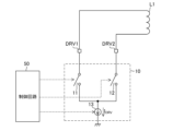
- FIG. 1 shows the overall configuration of an ultrasonic sensor 1 according to an embodiment of the present disclosure.
- the ultrasonic sensor 1 includes a piezoelectric element control IC2 (hereinafter referred to as IC2), a piezoelectric element 3, a transformer TR, a resistor RT , and capacitors CT , C1, and C2.
- IC2 is an example of a piezoelectric element processing device (or piezoelectric element control device).
- the IC 2 includes a transmitting circuit 10 , a receiving processing block 30 including a receiving circuit 31 , and a control circuit 50 .
- a ceramic vibrator ceramic piezoelectric element formed of ceramic can be used as the piezoelectric element 3, other types of piezoelectric elements may also be used.
- FIG. 2 is an external perspective view of the IC2.
- the IC2 includes a semiconductor chip having a semiconductor integrated circuit formed on a semiconductor substrate, a housing (package) that houses the semiconductor chip, and a plurality of external terminals exposed from the housing to the outside of the IC2. It is an electronic component.
- the IC 2 is formed by encapsulating a semiconductor chip in a housing (package) made of resin. Note that the number of external terminals of the IC 2 and the type of the casing of the IC 2 shown in FIG. 2 are merely examples, and they can be designed arbitrarily. FIG.
- FIG. 1 shows a power supply terminal PW, a ground terminal PGND, an output terminal DRV1, an output terminal DRV2, an input terminal IN1, an input terminal IN2, and a communication terminal CM, which are included in the plurality of external terminals. External terminals other than these are also provided on the IC2.
- Power supply voltage VCC is supplied to power supply terminal PW. Each circuit within IC2 is driven based on power supply voltage VCC. Power supply voltage VCC has a predetermined positive DC voltage value. An internal power supply circuit (not shown) that generates another internal power supply voltage from the power supply voltage VCC may be provided within the IC2. A ground terminal PGND is connected to ground.
- the transformer TR has a primary coil L1 and a secondary coil L2, and the primary coil L1 and the secondary coil L2 are magnetically coupled to each other while being electrically insulated from each other.
- a first end of the primary coil L1 is connected to an output terminal DRV1, and a second end of the primary coil L1 is connected to an output terminal DRV2.
- the power supply terminal PW is connected to the middle point (center tap) of the primary coil L1 via a resistor R0. More specifically, the power supply terminal PW is connected to one end of the resistor R0, and the other end of the resistor R0 is connected to the midpoint of the primary coil L1 and to the ground via the capacitor C0.
- a piezoelectric element 3 is connected in parallel to the secondary coil L2. That is, the first end of the secondary coil L2 is connected to the first end of the piezoelectric element 3, and the second end of the secondary coil L2 is connected to the second end of the piezoelectric element 3 and to the ground. . Further, a capacitor C T and a resistor R T are connected in parallel to the secondary coil L2. Furthermore, the first end of the secondary coil L2 and the first end of the piezoelectric element 3 are connected to the input terminal IN1 via the capacitor C1. That is, the first end of the secondary coil L2 and the first end of the piezoelectric element 3 are connected to the first end of the capacitor C1, and the second end of the capacitor C1 is connected to the input terminal IN1.
- the second end of the secondary coil L2 and the second end of the piezoelectric element 3 are connected to the input terminal IN2 via a capacitor C2. That is, the second end of the secondary coil L2 and the second end of the piezoelectric element 3 are connected to the first end of the capacitor C2, and the second end of the capacitor C2 is connected to the input terminal IN2. Note that the capacitors C1 and C2 may be built into the IC2.
- the ultrasonic sensor 1 uses the piezoelectric element 3 to transmit a transmission wave signal W1 in the ultrasonic band toward the external space of the ultrasonic sensor 1 (in a direction away from the ultrasonic sensor 1).
- a reflected wave signal W2 is generated by the transmitted wave signal W1 being reflected by the detection target object OBJ.
- the reflected wave signal W2 is received by the ultrasonic sensor 1 using the piezoelectric element 3.
- the ultrasonic band refers to a frequency band that is higher than the band of sound waves audible to the human ear and is inaudible to the human ear, and generally refers to a band of 20 kHz or higher.
- the transmitted wave signal W1 has a frequency within the range of 30kHz to 80kHz. Both the transmitted wave signal W1 and the reflected wave signal W2 belong to ultrasonic signals.
- the piezoelectric element 3 generates mechanical displacement (vibration) in itself according to a voltage signal applied between its first and second ends, and generates a transmission wave signal W1 by its mechanical displacement. Therefore, the piezoelectric element 3 functions as a transmitter for the transmission wave signal W1. Furthermore, the piezoelectric element 3 has a characteristic of generating an electromotive force between the first end and the second end in response to mechanical displacement (vibration) applied thereto, and also functions as a receiver for the reflected wave signal W2.
- the IC2 uses the piezoelectric element 3 to perform a transmission operation of the transmission wave signal W1 and a reception operation of the reflected wave signal W2.
- a transmission/reception operation the combination of the transmission operation of the transmission wave signal W1 and the reception operation of the reflected wave signal W2 may be referred to as a transmission/reception operation.
- the transmitting circuit 10 is connected to output terminals DRV1 and DRV2.
- the transmitting circuit 10 performs a transmitting operation of the transmitting wave signal W1 under the control of the control circuit 50.
- the transmission circuit 10 drives the piezoelectric element 3 by supplying an alternating current drive current to the primary coil L1. More specifically, in the transmission operation of the transmission wave signal W1, the transmission circuit 10 applies an AC voltage to the secondary coil L2 by supplying an AC drive current to the primary coil L1 via the output terminals DRV1 and DRV2. to occur.
- the receiving circuit 31 is connected to the input terminals IN1 and IN2, and performs a receiving operation of the reflected wave signal W2.
- the receiving circuit 31 uses the piezoelectric element 3 to receive the reflected wave signal W2 in the ultrasonic band. That is, the receiving circuit 31 receives the reflected wave signal W2 by receiving the voltage signal applied across the piezoelectric element 3 via the capacitors C1 and C2.
- the capacitors C1 and C2 remove the DC component of the voltage signal applied across the piezoelectric element 3, and only the AC component of the voltage signal applied across the piezoelectric element 3 is input to the receiving circuit 31 as the input signal Sin.
- the input signal Sin corresponds to the received signal of the reflected wave signal W2 by the receiving circuit 31.
- the input signal Sin also includes a voltage signal applied between both ends of the piezoelectric element 3 during the transmission operation of the transmitted wave signal W1.
- the reception processing block 30 performs necessary signal processing on the reflected wave signal W2 received by the reception circuit 31. Details of the reception processing block 30 will be described later. Note that the operation of each component of the reception processing block 30 is controlled by a control circuit 50.
- the ultrasonic sonar system shown in FIG. 4 can be formed.
- the ultrasonic sonar system in FIG. 4 includes a sensor module 5 formed by modularizing each component of the ultrasonic sensor 1, and an upper device 4.
- the ultrasonic sensor 1 is housed in the sensor module 5.
- a connector 6 connected to the ultrasonic sensor 1 within the sensor module 5 is provided in the sensor module 5 .
- the upper device 4 and the connector 6 are connected to each other via a harness 7.
- the harness 7 includes at least a power supply wiring to which a power supply voltage VCC is applied, a ground wiring to which a ground potential is applied, and a communication wiring.
- a power supply voltage VCC is supplied from the host device 4 to the ultrasonic sensor 1 (IC2) through power supply wiring.
- the communication wiring is connected to the host device 4 and also to the communication terminal CM of the IC 2 via the connector 6.
- the IC 2 and the higher-level device 4 perform bidirectional communication via the communication terminal CM and the communication wiring with reference to the ground potential. Communication between the IC2 and the higher-level device 4 is half-duplex communication, with the higher-level device 4 functioning as a master device and the IC2 functioning as a slave device. Any commands shown below are transmitted from the higher-level device 4 to the IC 2 via the communication wiring and received at the communication terminal CM. Furthermore, in the following description, any signal output (transmitted) from the IC 2 to the higher-level device 4 is input to the higher-level device 4 via the communication terminal CM and the communication wiring.
- the control circuit 50 executes a measurement operation when a predetermined measurement start condition is met.
- the upper-level device 4 can send a measurement instruction command to the IC 2.
- the measurement instruction command is received by the IC 2, the measurement start condition is established, and the control circuit 50 executes the measurement operation.
- a measurement operation is performed only once in response to reception of one measurement instruction command. However, the measurement operation may be repeated multiple times in response to reception of one measurement instruction command.
- the states of the upper-level device 4 and the IC 2 include a first communication state and a second communication state.
- the first communication state is a state in which the host device 4 functions as a transmitting device and the IC2 functions as a receiving device.
- a signal is sent from the host device 4 to the IC 2 via the communication wiring and the communication terminal CM. is sent.
- the second communication state is a state in which the host device 4 functions as a receiving device and the IC2 functions as a transmitting device.
- a signal is sent from the IC 2 to the host device 4 via the communication wiring and the communication terminal CM. is sent.
- the state of the upper-level device 4 and the IC 2 is the first communication state.
- the state of the host device 4 and the IC2 becomes the second communication state only during the execution period of the measurement operation, and returns to the first communication state when the measurement operation is completed.
- each measurement operation after the transmission operation of the transmitted wave signal W1 is performed, the reception operation of the reflected wave signal W2 is performed.
- the length of the execution period of the measurement operation is longer than the length of the execution period of the transmission operation. The length of the execution period of the measurement operation and the length of the execution period of the transmission operation are determined in advance prior to execution of the measurement operation.
- FIG. 6 is a diagram showing transmission and reception operations by the ultrasonic sensor 1.
- the control circuit 50 causes the transmission circuit 10 to perform a transmission operation of the transmission wave signal W1, and can transmit a signal 610 obtained by the reception operation of the reflected wave signal W2 to the upper-level device 4 in response to the transmission operation.
- the signal 610 is a binary signal having a high or low signal level, and corresponds to a signal S35 or S36 described later (see FIG. 8).
- a reception strength signal (corresponding to a reception strength signal S33 to be described later) having a signal value proportional to the strength (amplitude) of the input signal Sin is generated.
- the signal 610 has a high level, and if the value of the reception strength signal is equal to or greater than the determination threshold, the signal 610 has a low level.
- the upper-level device 4 can perform object detection processing based on the signal 610. Note that the proportionality constant between the intensity of the input signal Sin and the received intensity signal may change depending on the elapsed time from the transmission start time of the transmission wave signal W1.
- the object detection process may be a distance detection process that detects the distance between the ultrasonic sensor 1 and the detection target OBJ (in other words, the distance between the piezoelectric element 3 and the detection target OBJ).
- the ultrasonic sensor 1 and the detection target object OBJ can be derived.
- Time t1 represents the start time of transmission of the transmission wave signal W1 using the transmitter circuit 10 and piezoelectric element 3
- time t3 represents the start time of reception of the reflected wave signal W2 using the receiver circuit 31 and piezoelectric element 3.
- Time t2 represents the end time of transmission of the transmission wave signal W1 using the transmission circuit 10 and the piezoelectric element 3.
- Time t2 is a time before time t3.
- signal 610 Before time t1, signal 610 has a high level. Since an AC voltage with a sufficiently large amplitude is applied to the piezoelectric element 3 between times t1 and t2, the signal 610 becomes a low level, and returns to a high level after time t2. Thereafter, the reflected wave signal W2 from the object detection unit OBJ is received at time t3, thereby switching the signal 610 from high level to low level.
- the signal 610 is maintained at a low level, and the signal 610 switches from low level to high level at time t4.
- the length between times t3 and t4 is ideally equal to the length between times t1 and t2.
- the object detection process may be an approach detection process.
- the host device 4 receives the reflected wave signal W2 before a predetermined time elapses after transmitting the transmitted wave signal W1 at time t1, the host device 4 determines that the ultrasonic sensor 1 is a detection target. It is determined that the object OBJ is approaching, and if not, it is determined that the detection target object OBJ is not approaching the ultrasonic sensor 1.
- time t2 if the signal 610 switches from a high level to a low level within a predetermined time from time t1, the host device 4 detects that the object to be detected OBJ approaches the ultrasonic sensor 1. If not, it can be determined that the object to be detected OBJ is not approaching the ultrasonic sensor 1.
- the ultrasonic sensor 1 is mounted on any device.
- a device equipped with the ultrasonic sensor 1 will be referred to as a sensor-equipped device.
- An ultrasonic sonar system (see FIG. 4) having an upper-level device 4 and a sensor module 5 may be installed in a sensor-equipped device.
- a typical example of a sensor-equipped device is a vehicle such as an automobile. It can also be said that the distance between the ultrasonic sensor 1 and the detection target OBJ corresponds to the distance between the sensor mounting device and the detection target OBJ. It can also be said that the approach of the detection target OBJ to the ultrasonic sensor 1 corresponds to the approach of the detection target OBJ to the sensor mounting device.
- the piezoelectric element 3 continues to vibrate for a while based on the mechanical energy accumulated during the supply period of the drive current.
- the vibration of the piezoelectric element 3 after the supply of drive current is stopped is called reverberation. If the duration of reverberation is long, it becomes difficult to detect objects at close range.
- a capacitor C T and a resistor R T are provided to reduce reverberation.
- a resistor was inserted between the capacitor C1 and the input terminal IN1
- a resistor was inserted between the capacitor C2 and the input terminal IN2
- a resistor was inserted between the input terminals IN1 and IN2. It is good that a capacitor is inserted.
- FIG. 7 shows the internal configuration of the transmitting circuit 10 and the relationship between the transmitting circuit 10 and the control circuit 50.
- the transmitting circuit 10 includes switching elements 11 and 12 and a current source 13.
- a first end (first electrode) of the switching element 11 is connected to the output terminal DRV1, and therefore connected to the first end of the primary coil L1.
- a second end (second electrode) of the switching element 11 is connected to an input end of the current source 13.
- the first end (first electrode) of the switching element 12 is connected to the output terminal DRV2, and therefore connected to the second end of the primary coil L1.
- a second end (second electrode) of the switching element 12 is connected to an input end of the current source 13.
- the current source 13 is a constant current source having an input end and an output end, and operates so that the drive current I DRV flows from its own input end to its own output end.
- the output end of current source 13 is connected to ground.
- the drive current I DRV flows from the input end of the current source 13 toward the output end (therefore, the ground).
- the control circuit 50 can individually control the on and off states of the switching elements 11 and 12. In the transmission operation of the transmission wave signal W1, the control circuit 50 supplies an alternating current drive current to the primary coil L1 by alternately turning on and off the switching elements 11 and 12. More specifically, in the transmission operation, the control circuit 50 alternately switches the state of the transmission circuit 10 between the first drive state and the second drive state.
- switching elements 11 and 12 are on and off, respectively. Therefore, in the first drive state, the first end of the primary coil L1 is electrically connected to the current source 13 through the output terminal DRV1 and the switching element 11, and due to the action of the current source 13, the first end of the primary coil L1 is connected to the output terminal.
- a drive current I DRV flows toward the current source 13 through the DRV 1 and the switching element 11 . Note that the drive current I DRV in the first drive state flows through an electric path passing through the capacitor C0, the center tap of the primary coil L1, and the first end of the primary coil L1 (see also FIG. 1).
- switching elements 11 and 12 are off and on, respectively. Therefore, in the second drive state, the second end of the primary coil L1 is electrically connected to the current source 13 through the output terminal DRV2 and the switching element 12, and due to the action of the current source 13, the second end of the primary coil L1 is connected to the output terminal.
- a drive current I DRV flows toward the current source 13 through the DRV 2 and the switching element 12 .
- the drive current I DRV in the second drive state flows through an electric path passing through the capacitor C0, the center tap of the primary coil L1, and the second end of the primary coil L1 (see also FIG. 1).
- Each of the switching elements 11 and 12 is constituted by, for example, a P-channel type MOSFET (metal-oxide-semiconductor field-effect transistor).
- the sources of the switching elements 11 and 12 may be connected to the output terminals DRV1 and DRV2, respectively, while the drains of the switching elements 11 and 12 may be connected to the input terminal of the current source 13.
- the control circuit 50 may individually control the on/off states of the switching elements 11 and 12 by controlling the gate potentials of the switching elements 11 and 12.
- the switching elements 11 and 12 may be configured with N-channel MOSFETs.
- the current source 13 may be a variable current source configured to be able to change the value of the drive current I DRV , and the control circuit 50 may be able to adjust the value of the drive current I DRV .
- FIG. 8 shows an internal block diagram of the reception processing block 30.
- the reception processing block 30 includes a reception circuit 31, an ADC 32, a signal processing circuit 33, a comparison signal generation circuit 34, a comparison circuit 35, a filter circuit 36, a signal selection circuit 37, a DAC 38, a switching output circuit 39, and a selection designation circuit 40. .
- the operations of the components (31 to 40) of the reception processing block 30 are controlled by a control circuit 50.
- the receiving circuit 31 is connected to the input terminals IN1 and IN2 as described above.
- a signal between input terminals IN1 and IN2 indicates an alternating current component of a voltage signal applied between both ends of piezoelectric element 3, and is input to receiving circuit 31 as input signal Sin.
- the receiving circuit 31 performs a signal amplification process to amplify the input signal Sin, and generates and outputs the amplified input signal Sin as an amplified received signal S31.
- the amplified received signal S31 is an analog signal having an amplitude proportional to the amplitude of the input signal Sin.
- the amplified received signal S31 is input to the ADC 32.
- the ADC 32 is an A/D converter (analog/digital converter), and generates and outputs a signal S32 by converting the amplified received signal S31 into a digital signal. Since the signal S32 is a signal obtained by converting the amplified received signal S31 expressed in the analog domain into a signal expressed in the digital domain, the signal S32 can also be referred to as an amplified received signal.
- the digital amplified reception signal S32 is input to the signal processing circuit 33.
- the signal processing circuit 33 generates and outputs a reception strength signal S33 by performing predetermined signal processing on the amplified reception signal S32.
- the reception strength signal S33 is a signal indicating the strength of the input signal Sin (that is, a signal indicating the strength of the reception signal at the reception circuit 31).
- the reception strength signal S33 is a digital signal (signal in the digital domain), and the greater the strength of the input signal Sin at a certain time, the greater the value of the reception strength signal S33 at that time.
- the signal processing in the signal processing circuit 33 includes envelope detection for detecting the envelope of the amplified received signal S32.
- the intensity (amplitude) of the input signal Sin can be specified by detecting the envelope of the amplified received signal S32.
- the signal processing in the signal processing circuit 33 may further include processing other than envelope detection (for example, digital filtering). Note that the content of the signal processing in the signal processing circuit 33 is arbitrary as long as a signal indicating the strength of the input signal Sin (that is, a signal indicating the strength of the received signal at the receiving circuit 31) can be generated as the reception strength signal S33.
- the signal processing circuit 33 is an example of a reception strength signal generation circuit. It may be considered that the ADC 32 and the signal processing circuit 33 form a reception strength signal generation circuit.
- the comparison signal generation circuit 34 generates and outputs a comparison signal S34, which is a signal to be compared with the reception strength signal S33.
- the comparison signal S34 is a digital signal (signal in the digital domain), and the value of the comparison signal S34 is sometimes particularly referred to as a determination threshold value.
- the determination threshold value that is, the value of the comparison signal S34 changes with the passage of time from the transmission start time of the transmission wave signal W1.
- the reception strength signal S33 and comparison signal S34 are input to the comparison circuit 35.
- Comparison circuit 35 compares reception strength signal S33 and comparison signal S34, and outputs signal S35 indicating the comparison result.
- Signal S35 and signal S36 which will be described later, are binary signals having a value of "1" or "0". Here, it is assumed that the "1" signals S35 and S36 have a low level, and the "0" signals S35 and S36 have a high level.
- the comparison circuit 35 outputs a signal S35 of "1” if the value of the reception strength signal S33 is equal to or greater than the value of the comparison signal S34, and outputs a signal S35 of "1” if the value of the reception strength signal S33 is less than the value of the comparison signal S34.
- a signal S35 of 0'' is output. Signals S35 and S36 may especially be referred to as comparison result signals.
- the comparison result signal S35 is input to the filter circuit 36.
- the filter circuit 36 performs filtering processing on the comparison result signal S35 with the main purpose of reducing noise contained in the comparison result signal S35, and outputs the comparison result signal S35 after the filtering process as a comparison result signal S36. Note that in the reception processing block 30, the function of the filter circuit 36 may be disabled or the filter circuit 36 may not be provided. In that case, the comparison result signal S36 indicates exactly the same thing as the comparison result signal S35.
- a reception strength signal S33 and a comparison signal S34 are input to the signal selection circuit 37.
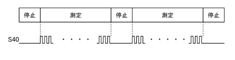
- the selection designation signal S40 from the selection designation circuit 40 is also input to the signal selection circuit 37.
- the selection designation signal S40 is a binary signal having a value of "1" or "0".
- the signal selection circuit 37 selects either the reception strength signal S33 or the comparison signal S34 in response to the selection designation signal S40, and outputs the selected signal as the signal S37.
- the selection designation signal S40 has a value of "1”
- the reception strength signal S33 is selected as the signal S37
- the comparison signal S34 is selected as the signal S37. shall be selected as.
- Signal S37 may hereinafter be referred to as selection signal S37.
- the selection signal S37 is input to the DAC38.
- the DAC 38 is a D/A converter (digital/analog converter), and generates and outputs a signal S38 by converting the selection signal S37 into an analog signal.
- Signal S38 may hereinafter be referred to as DAC output signal S38.
- the analog DAC output signal S38 is input to the switching output circuit 39.
- the switching output circuit 39 outputs either the comparison result signal S36 or the DAC output signal S38 from the communication terminal CM as the IC output signal S39 under the control of the control circuit 50.
- the IC output signal S39 output from the communication terminal CM is transmitted to the host device 4 via the communication wiring.
- a signal output circuit 41 is formed by the signal selection circuit 37, DAC 38, switching output circuit 39, and selection designation circuit 40.
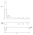
- FIG. 9 shows waveform examples of signals S33, S34, and S35 in one measurement operation.
- the reception strength signal S33 is shown by a broken line waveform
- the comparison signal S34 and comparison result signal S35 are shown by a solid line waveform. If noise and the like are ignored, the waveforms of the comparison result signal S35 and the comparison result signal S36 shown in FIG. 9 are substantially the same.
- One measurement operation starts at time t1 and ends at time t10.
- the control circuit 50 executes the measurement operation using the transmitting circuit 10 and the components (31 to 40) of the receiving processing block 30. It may be considered that under the control of the control circuit 50, the transmitting circuit 10 and the components (31 to 40) of the receiving processing block 30 cooperate to execute the measurement operation.
- Time t2 is a time before time t10, which corresponds to the end time of the execution period of the measurement operation.
- a transmission wave signal W1 is transmitted from the piezoelectric element 3 between times t1 and t2. Transmission of the transmission wave signal W1 is stopped at time t2.
- times t1 and t2 described here correspond to times t1 and t2 described above with reference to FIG. 6, and times t3 and t4 described above are times before time t10.
- the length of the execution period of the transmission operation is the transmission setting time T O corresponding to the length between times t1 and t2, and the length of the execution period of the measurement operation is the measurement setting time corresponding to the length between times t1 and t10.
- the time is T M.
- the transmission set time T O and the measurement set time T M are determined in advance prior to execution of the measurement operation. It may be considered that the control circuit 50 sets the transmission set time T O and the measurement set time T M.
- the transmission setting time T O and the measurement setting time T M can be changed based on a setting command transmitted from the upper-level device 4 and received by the IC 2.
- the comparison result signal S35 becomes a low level, and returns to a high level after time t2. Thereafter, the comparison result signal S35 becomes low level only during the period in which the value of the reception strength signal S33 is greater than or equal to the value of the comparison signal S34.
- the comparison signal generation circuit 34 sets the determination threshold (that is, the value of the comparison signal S34) to the transmission start time of the transmission wave signal W1. It changes with the passage of time from t1. For example, when the ultrasonic sonar system is mounted on a vehicle that runs on a road surface, the road surface is excluded from the detection target object OBJ. At this time, in order to avoid erroneously detecting the road surface as the detection target object OBJ based on the reflected waves from the road surface, the determination threshold value is set relatively in the time period when the reflected waves from the road surface are received by the receiving circuit 31. Things like raising the price are done. Further, the comparison signal S34 is set in consideration of the fact that as the distance between the detection target object OBJ and the ultrasonic sensor 1 increases, the intensity of the reflected wave signal W2 received by the receiving circuit 31 decreases.
- determination threshold data that specifies how to change the value of the comparison signal S34 from time t1 to time t10 is stored in the control circuit 50 or the comparison signal generation circuit 34, and the comparison signal generation circuit 34
- the circuit 34 may generate and output the comparison signal S34 based on the determination threshold data.
- the determination threshold data may be changed based on a setting command transmitted from the upper-level device 4 and received by the IC 2.
- the comparison signal generation circuit 34 may change the determination threshold depending on the gain of signal amplification in the reception circuit 31 or the signal processing circuit 33.
- the signal output circuit 41 operates in one of a plurality of output modes.
- the control circuit 50 designates and controls which output mode the signal output circuit 41 operates in.
- the control circuit 50 sets any one of the plurality of output modes to the target output mode according to the mode designation command received from the host device 4, and the signal output circuit 41 operates in the target output mode.
- the plurality of output modes include output modes MD A and MD B.
- the output mode MD A will be explained.
- the target output mode is output mode MD A.
- the output mode MD A is used in the actual operation stage where the ultrasonic sonar system is mounted on a sensor-equipped device (such as a vehicle) and object detection processing is performed.
- the output mode MD A is used in the actual operation stage where the ultrasonic sonar system is mounted on a sensor-equipped device (such as a vehicle) and object detection processing is performed.
- the output mode MD A that is, when the output mode MD A is set to the target output mode
- the comparison result signal S36 is sent to the communication terminal as the IC output signal S39 throughout the execution period of the measurement operation. Output from CM.
- the signal output circuit 41 operates as a comparison circuit from the transmission start time (t1) of the transmission wave signal W1 until the measurement set time T M elapses (that is, until the measurement operation ends).
- a signal based on the comparison result of No. 35 is output from the communication terminal CM.
- the host device 4 can perform the above-described object detection process based on the IC output signal S39 in the output mode MD A.
- the control circuit 50 operates the signal selection circuit 37, DAC 38, and selection designation circuit 40 during a period in which the DAC output signal S38 is output as the IC output signal S39, and operates the signal selection circuit 37, DAC 38, and selection designation circuit 40 in other periods.
- the operation of the circuit 40 is stopped. Therefore, in the output mode MD A (that is, when the output mode MD A is set to the target output mode), the control circuit 50 stops the operations of the signal selection circuit 37, DAC 38, and selection designation circuit 40.
- the switching output circuit 39 may have a configuration as shown in FIG.
- the switching output circuit 39 in FIG. 10 has an I/F circuit 39a.
- the comparison result signal S36 is input to the input terminal of the I/F circuit 39a.
- An output terminal of the I/F circuit 39a is connected to a communication terminal CM.
- the I/F circuit 39a operates effectively during the period in which the comparison result signal S36 is to be output as the IC output signal S39, and outputs the comparison result signal S36 as the IC output signal S39 from the communication terminal CM during this period. At this time, necessary level shift processing and the like are executed as appropriate.
- the output terminal of the DAC 38 is connected to the communication terminal CM together with the output terminal of the I/F circuit 39a. However, when the operation of the DAC 38 is stopped, the input impedance of the output terminal of the DAC 38 is sufficiently high when viewed from the communication terminal CM. Therefore, in the measurement operation in the output mode MD A , the IC output signal S39 corresponding to the comparison result signal S36 can be output from the communication terminal CM through the I/F circuit 39a.
- the DAC output signal S38 can be output from the communication terminal CM as the IC output signal S39.
- debugging work work including adjustment of determination thresholds and the like (hereinafter referred to as debugging work) is performed.
- the worker responsible for the debugging work desires to refer to various internal signals within the IC2.
- the IC 2 has the configuration and output mode MD B shown in FIG. 8.
- some reference configurations are shown below.
- the components 37 to 40 shown in FIG. 8 are not provided, and only the comparison result signal S36 can be output from the communication terminal CM.
- a wiring WR is drawn out from the IC exclusively for debugging work, and a signal on the wiring WR (for example, a signal at S33 or S34) is observed using a special jig or the like. do.
- a step of drawing out the wiring WR from the IC exclusively for debugging is required, which is inconvenient.
- the components 37 and 40 shown in FIG. 8 are not provided.
- the comparison result signal S36 or the reception strength signal S33 can be switched and output from the communication terminal CM. Therefore, during debugging work related to the second reference configuration, the operator can easily observe the reception strength signal S33. However, in the second reference configuration, only the reception strength signal S33 can be observed during debugging, making it difficult to proceed with the debugging.
- Output mode MD B The configuration and output mode MD B shown in FIG. 8 facilitate debugging work.
- the signal output circuit 41 outputs m types of output target signals from the communication terminal CM while switching them.
- m is an arbitrary integer of 2 or more.
- the m types of output target signals are composed of output target signals S[1] to S[m].
- any two mutually different natural numbers less than or equal to m are represented by i A and i B.
- the output target signal S[i A ] is a signal representing the waveform of the reception strength signal S33
- the output target signal S[i B ] is a signal representing the waveform of the comparison signal S34. That is, any two of the output target signals S[1] to S[m] are a signal representing the waveform of the reception strength signal S33 and a signal representing the waveform of the comparison signal S34.
- the output target signal S[i A ] is the DAC output signal S38 when the reception strength signal S33 is the selection signal S37, that is, the reception strength signal S33 is converted into an analog signal.
- the output target signal S[i A ] may be any signal that represents the waveform of the reception strength signal S33.
- the output target signal S[i B ] is the DAC output signal S38 when the comparison signal S34 is the selection signal S37, that is, the comparison signal S34 is converted into an analog signal.
- the output target signal S[i B ] may be any signal that represents the waveform of the comparison signal S34.
- a debugging worker can easily observe the waveform of the received strength signal S33 and the waveform of the comparison signal S34 based on the signal output from the communication terminal CM, and make a decision. Debugging work including threshold adjustment etc. can be performed efficiently.
- output mode MD B is output mode MD B1 .
- "m 2"
- the signal output circuit 41 outputs the output target signal from the transmission start time (t1) of the transmission wave signal W1 until the measurement set time T M elapses (that is, until the measurement operation ends).
- S[1] and S[2] are sequentially switched and output from the communication terminal CM.
- Outputting from the communication terminal CM while sequentially switching the output target signals S[1] and S[2] means, in other words, outputting from the communication terminal CM while switching the output target signals S[1] and S[2] alternately. It corresponds to doing.
- the switching period of the signal output from the communication terminal CM in the output mode MD B1 is represented by the symbol "P SW ".
- the signal output from the communication terminal CM is switched between the output target signals S[1] and S[2] every time the switching period P SW elapses.
- the switching period P SW is sufficiently shorter than the measurement setting time T M . Therefore, in the measurement operation related to the output mode MD B1 , the signal output circuit 41 outputs the output target signals S[1] and S[ with a cycle shorter than the measurement setting time T M (that is, a cycle shorter than the execution period of the measurement operation). 2] is output from the communication terminal CM while being switched periodically (alternately).
- the sensor driving frequency is 50 to 60 kHz (kilohertz).
- the sensor drive frequency represents the frequency of the AC voltage applied to the piezoelectric element 3 during the transmission operation of the transmission wave signal W1, and in the configuration of FIG. 1, is equal to the frequency of the AC current supplied to the primary coil L1.
- the reciprocal of the sensor drive frequency is called the sensor drive period.
- the switching period P SW may be about several tens of microseconds.
- the update period of any digital signal in the reception processing block 30 may match the sensor drive period, and in this case, for example, the switching period P SW may be 1/2 of the sensor drive period (however, 1/2 is just an example and can be modified in various ways).
- FIG. 14 schematically shows the waveform of the IC output signal S39 during the execution period of the measurement operation related to the output mode MD B1 .
- waveforms 711 and 712 are shown on the display screen of the oscilloscope.
- the waveform 711 is shown as a broken line waveform
- the waveform 712 is shown as a solid line waveform.
- the waveform 711 is the waveform of the output target signal S[1], and thus represents the waveform of the reception strength signal S33.
- the waveform 712 is the waveform of the output target signal S[2], and thus represents the waveform of the comparison signal S34.
- FIG. 15 is an enlarged view (enlarged view in the time direction) of waveforms 711 and 712 around time t2. It can be seen that the IC output signal S39 is switched between the output target signals S[1] and S[2] every time the switching period P SW elapses. Since the switching period P SW is sufficiently short with respect to the measurement setting time T M , when the waveform of the IC output signal S39 is observed with an oscilloscope on the entire scale of the measurement setting time T M , the waveforms 711 and 712 are overlapped. observed at the same time. That is, the debugging worker can simultaneously observe the waveform of the reception strength signal S33 and the comparison signal S34, and can efficiently perform the debugging work.
- FIG. 16 shows the waveform of the selection designation signal S40 in the output mode MD B1 .
- the value of the selection designation signal S40 alternately changes between “1” and “0” every time the switching period P SW elapses.
- the selection signal S37 is the reception strength signal S33 when the selection designation signal S40 has a value of "1”, and is the comparison signal S34 when the selection designation signal S40 has a value of "0".
- the value of the selection designation signal S40 during the non-execution period of the measurement operation is arbitrary, but in the example of FIG. 16, it is fixed at "0".
- output mode MD B is output mode MD B2 .
- "m 2"
- the output target signals S[1] and S[2] are alternately switched and output from the communication terminal CM during each measurement operation.
- the signal output from the communication terminal CM is switched between the output target signals S[1] and S[2] every time one measurement operation is performed. .
- the signal output circuit 41 operates from the transmission start time (t1) of the transmission wave signal W1 until the measurement set time T M has elapsed (that is, until the measurement operation ends). , outputs only one of the output target signals S[1] and S[2] from the communication terminal CM.
- the signal output circuit 41 outputs the signal output from the communication terminal CM to the output target signals S[1] and S every time one measurement operation is executed. [2] Switch alternately between.
- FIG. 17 schematically shows the waveform of the IC output signal S39 in the output mode MD B2 .
- the i-th measurement operation is performed between times t21 and t22, then the (i+1)-th measurement operation is performed between times t23 and t24, and further thereafter, the i-th measurement operation is performed between times t25 and t24.
- the (i+2)th measurement operation is performed between times t26 and then the (i+3)th measurement operation is performed between times t27 and t28.
- i is any natural number.
- the signal output circuit 41 outputs the output target signal S[1] from the communication terminal CM in the i-th measurement operation, and outputs the output target signal S[2] from the communication terminal CM in the (i+1)th measurement operation. Then, in the (i+2)th measurement operation, the output target signal S[1] is output from the communication terminal CM, and in the (i+3)th measurement operation, the output target signal S[2] is output from the communication terminal CM.
- the waveform of the IC output signal S39 in FIG. 17 is a waveform 721 between times t21 and t22, a waveform 722 between times t23 and t24, a waveform 723 between times t25 and t26, and a waveform 724 between times t27 and t28. ,including.
- the waveform 721 is the waveform of the output target signal S[1] between times t21 and t22, and therefore represents the waveform of the reception strength signal S33 between times t21 and t22.
- the waveform 722 is the waveform of the output target signal S[2] between times t23 and t24, and therefore represents the waveform of the comparison signal S34 between times t23 and t24.
- the waveform 723 is the waveform of the output target signal S[1] between times t25 and t26, and therefore represents the waveform of the reception strength signal S33 between times t25 and t26.
- the waveform 724 is the waveform of the output target signal S[2] between times t27 and t28, and therefore represents the waveform of the comparison signal S34 between times t27 and t27.
- a waveform in which waveforms 721 to 724 are arranged along the time axis direction as shown in FIG. 17 is observed.
- Many oscilloscopes are equipped with an afterimage display function that displays a waveform once displayed on the display screen as an afterimage.
- the afterimage display function waveforms 721' and 722' as shown in FIG. 18 can be displayed in a superimposed manner on the display screen of the oscilloscope.
- a solid line waveform 722' corresponds to the waveform 722 in FIG. 17
- a broken line waveform 721' corresponds to the waveform 721 in FIG.
- the waveform 721' is displayed superimposed on the waveform 722' by the afterimage display function.
- the output mode MD B2 also allows debugging workers to observe the waveform of the reception strength signal S33 and the comparison signal S34, and by using the afterimage display function, etc., these waveforms can be observed simultaneously. You can also do it. Therefore, debugging work can be performed efficiently.
- FIG. 19 shows the waveform of the selection designation signal S40 in the output mode MD B2 .
- the output mode MD B1 according to the first embodiment and the output mode MD B2 according to the second embodiment will be compared.
- the waveforms of the reception strength signal S33 and the comparison signal S34 obtained in the same measurement operation can be observed simultaneously, so there is an advantage that no mismatch occurs between the waveforms.
- CR filters or slew rate control are often applied to signals propagated to communication wiring as a countermeasure against EMI or malfunction.
- the waveform observed as the IC output signal S39 may not correctly represent the waveform of the signal S33 or S34 because the output tracking is not in time due to the need for high-speed switching. . Therefore, set the switching period P SW to be longer, or lower the value of the pull-up resistor connected to the communication wiring (assuming that a method is adopted in which signal transmission is performed depending on whether or not current flows through the pull-up resistor). ) may be necessary.
- the signal switching period is quite long, so there is no concern about output tracking.
- the reception strength signal S33 and the comparison signal S34 observed in the output mode MD B2 are not signals acquired during the same measurement operation, there is a possibility that a mismatch will occur between their waveforms ( (There may be a deviation in the relationship between the determination threshold and the received signal strength.)
- the output mode MD B (ie, the output mode MD B1 ) according to the first embodiment can be modified to suit the condition of "m ⁇ 3".
- the output mode MD B subjected to this modification is referred to as an output mode MD B3 .
- the output mode MD B according to the third embodiment is the output mode MD B3 , and "m ⁇ 3" in the third embodiment. Note that when "m ⁇ 3", the configuration of the signal output circuit 41 may be modified from the configuration shown in FIG. 8 as appropriate.
- the signal output circuit 41 outputs the output target signal from the transmission start time (t1) of the transmission wave signal W1 until the measurement set time T M has elapsed (that is, until the measurement operation ends). Output from the communication terminal CM while sequentially switching S[1] to S[m].
- the signal output from the communication terminal CM is sequentially switched between the output target signals S[1] to S[m] every time the switching period P SW elapses. As described above, the switching period P SW is sufficiently shorter than the measurement setting time T M .
- the signal output circuit 41 outputs the output target signals S[1] to S[ with a cycle shorter than the measurement setting time T M (that is, a cycle shorter than the execution period of the measurement operation). m] is outputted from the communication terminal CM while sequentially switching periodically.
- the signal output from the communication terminal CM changes from the output target signal S[1] to the output target signal S every time the switching period P SW elapses. [m], the output target signals S[1], S[2], S[3]...S[m] are sequentially switched.
- the switching period P SW has elapsed after the output target signal S[m] started being output from the communication terminal CM
- the signal output from the communication terminal CM returns to the output target signal S[1], and the same switching output is performed thereafter. It will be done.
- the output target signal S[1] is a signal representing the waveform of the reception strength signal S33
- the output target signal S[2] is a signal for comparison. This signal represents the waveform of signal S34. Any signal within the IC2 can be set as the output target signals S[3] to S[m].
- a lower limit analog signal representing the lower limit potential of the DAC output signal S38 or an upper limit analog signal representing the upper limit potential of the DAC output signal S38 is set to any of the output target signals S[3] to S[m]. It's good.
- the DAC output signal S38 is an analog signal having a potential from a lower limit signal level (zero scale level) to an upper limit signal level (full scale level). Therefore, in the configuration of FIG. 8, when the DAC output signal S38 becomes the IC output signal S39, the output target signals S[1] to S[m] all have potentials from the lower limit signal level to the upper limit signal level.
- the potential of the upper limit signal level is higher than the potential of the lower limit signal level.
- the waveforms 721 to 724 in FIG. 17, or the waveforms 721' and 722' in FIG. It is difficult to recognize the upper limit signal level (full scale level).
- the waveform of the observation target signal for example, waveforms 711 and 712 in FIG. 14
- the lower limit signal level cannot be clearly recognized, it is possible to determine whether noise is superimposed on the observation target signal and whether the noise is superimposed on the observation target signal. Difficult to grasp the degree etc.
- the waveform of the observation target signal (for example, waveforms 711 and 712 in FIG. 14) is displayed on the display screen of the oscilloscope, and the upper limit signal level cannot be clearly recognized, it is difficult to determine whether the observation target signal has reached the upper limit signal level. or the difference between the level of the signal to be observed and the upper limit signal level.
- the output mode MD B (ie, the output mode MD B2 ) according to the second embodiment can be modified to suit the condition of "m ⁇ 3".
- the output mode MD B subjected to this modification is referred to as an output mode MD B4 .
- the output mode MD B according to the fourth embodiment is the output mode MD B4 , and "m ⁇ 3" in the fourth embodiment. Note that when "m ⁇ 3", the configuration of the signal output circuit 41 may be modified from the configuration shown in FIG. 8 as appropriate.
- the signal output circuit 41 In the measurement operation related to the output mode MD B4 , the signal output circuit 41 outputs the output target signal from the transmission start time (t1) of the transmission wave signal W1 until the measurement set time T M has elapsed (that is, until the measurement operation ends). Any one of S[1] to S[m] is continuously output from the communication terminal CM.
- the signal output circuit 41 When the measurement operation is repeatedly executed multiple times in the output mode MD B4 , the signal output circuit 41 outputs the signal output from the communication terminal CM as the output target signals S[1] to S every time one measurement operation is executed. Switch sequentially between [m].
- the signal output from the communication terminal CM changes from the output target signal S[1] to the output target signal every time one measurement operation is executed.
- the output target signals S[1], S[2], S[3]...S[m] are sequentially switched toward S[m].
- the signal output from the communication terminal CM in the next measurement operation returns to the output target signal S[1]. Thereafter, similar switching output is performed.
- the output target signal S[1] is a signal representing the waveform of the reception strength signal S33
- the output target signal S[2] is a signal for comparison.
- This signal represents the waveform of signal S34.
- Any signal within the IC2 can be set as the output target signals S[3] to S[m].
- the lower limit analog signal or the upper limit analog signal may be set as one output target signal.
- the signal output circuit 41 may operate in any of the first to nth output modes.
- n is an arbitrary integer of 2 or more.
- the output mode MD A is the first output mode.
- it is basically assumed that "n 2", but "n ⁇ 3" may be satisfied.
- any one or more output modes among the above output modes MD B1 , MD B2 , MD B3_1 , MD B3_2 , MD B3_3 , MD B4_1 , MD B4_2 and MD B4_3 are set as the second to nth output modes.
- the output modes MD B1 , MD B2 , MD B3_1 , MD B3_2 , MD B3_3 , MD B4_1 , MD B4_2 and MD B4_3 may be the second to ninth output modes, respectively.
- the control circuit 50 specifies and controls in which output mode the signal output circuit 41 operates.
- the control circuit 50 sets any one of the first to nth output modes to the target output mode in accordance with the mode designation command received from the host device 4, and the signal output circuit 41 operates in the target output mode.
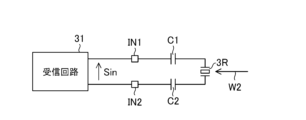
- the single piezoelectric element 3 functions as a transmitter for the transmitted wave signal W1 and as a receiver for the reflected wave signal W2.
- a piezoelectric element 3R as a wave receiver may be separately provided as shown in FIG.
- the piezoelectric element 3 is not connected to the capacitors C1 and C2, but instead the first end of the piezoelectric element 3R is connected to the first end of the capacitor C1, and the second end of the capacitor C1 is connected to the input terminal IN1.
- the piezoelectric element 3R is arranged at a position separated from the piezoelectric element 3, and receives the reflected wave signal W2 to generate a voltage signal between both ends of the piezoelectric element 3R.
- the receiving circuit 31 is connected to the input terminals IN1 and IN2, and performs a receiving operation of the reflected wave signal W2.
- the receiving circuit 31 receives the reflected wave signal W2 in the ultrasonic band using the piezoelectric element 3R. That is, the receiving circuit 31 receives the reflected wave signal W2 by receiving the voltage signal applied across the piezoelectric element 3R via the capacitors C1 and C2.
- the capacitors C1 and C2 remove the DC component of the voltage signal applied across the piezoelectric element 3R, and only the AC component of the voltage signal applied across the piezoelectric element 3R is input to the receiving circuit 31 as the input signal Sin.
- the input signal Sin corresponds to the received signal of the reflected wave signal W2 by the receiving circuit 31. It is as described above except that the piezoelectric element that generates the input signal Sin is the piezoelectric element 3R.
- a configuration in which the transformer TR is not provided in the ultrasonic sensor 1 may be adopted.
- the output terminals DRV1 and DRV2 are directly connected to the first and second ends of the piezoelectric element 3, respectively, and in the transmission operation, the transmitting circuit 10 supplies an AC voltage of a predetermined amplitude between both ends of the piezoelectric element 3.
- the piezoelectric element 3 may be driven by the following.
- the upper-level device 4 is, for example, an ECU (Electronic Control Unit) mounted on the vehicle.
- ECU Electronic Control Unit
- the ECU can perform object detection processing.
- the IC 2 may be operated in the output mode MD B with the ultrasonic sensor 1 connected to the ECU, and in this case, the ECU can be used for debugging.
- a device dedicated to debugging work may be used as the upper-level device 4.
- a piezoelectric element processing device (2) includes a transmitting circuit (10) configured to transmit a transmission wave signal (W1) from the piezoelectric element by driving the piezoelectric element (3). , a receiving circuit (31) configured to receive a reflected wave signal (W2) of the transmitted wave signal by an object using the piezoelectric element or another piezoelectric element (3R); A reception strength signal generation circuit (33) configured to generate a reception strength signal (S33) representing the strength, and a comparison signal (33) whose signal value changes as time elapses from the transmission start time of the transmission wave signal.
- a comparison signal generation circuit (34) configured to generate a signal S34), a comparison circuit (35) configured to compare the reception strength signal and the comparison signal, and a signal generation circuit (35) configured to generate a signal from a communication terminal (CM).
- a signal output circuit (41) configured to be able to output a A first output mode (MD A ) in which a signal is output from the communication terminal, and a second output mode (MD B ), and the plurality of output target signals include a signal representing the waveform of the received strength signal and a signal representing the waveform of the comparison signal, and two output target signals (S[1] and S[2] ) (first configuration).
- a measurement operation is performed using the transmission circuit, the reception circuit, the reception strength signal generation circuit, the comparison signal generation circuit, the comparison circuit, and the signal output circuit.
- the measurement operation includes a transmission operation of causing the transmission circuit to transmit the transmission wave signal for a transmission setting time, and the measurement operation in the first output mode.
- the signal output circuit outputs a signal based on the comparison result of the comparison circuit from the communication terminal, and in the measurement operation in the second output mode, the signal output circuit outputs the plurality of output target signals.
- a configuration (second configuration) may be adopted in which output is output from the communication terminal while sequentially switching.
- the signal output circuit in the measurement operation in the second output mode, the signal output circuit outputs the plurality of outputs at a cycle (P SW ) shorter than the execution period of the measurement operation.
- a configuration (third configuration) may be adopted in which the target signal is outputted from the communication terminal while being periodically and sequentially switched.
- a measurement operation is performed using the transmission circuit, the reception circuit, the reception strength signal generation circuit, the comparison signal generation circuit, the comparison circuit, and the signal output circuit.
- the measurement operation includes a transmission operation of causing the transmission circuit to transmit the transmission wave signal for a transmission setting time, and the measurement operation in the first output mode.
- the signal output circuit outputs a signal based on the comparison result of the comparison circuit from the communication terminal, and in the measurement operation in the second output mode, the signal output circuit outputs a signal based on the comparison result of the comparison circuit, and in the measurement operation in the second output mode, the signal output circuit outputs a signal based on the comparison result of the comparison circuit.
- the signal output circuit When one of the signals is output from the communication terminal and the measurement operation is repeatedly executed a plurality of times in the second output mode, the signal output circuit outputs the signal from the communication terminal each time the measurement operation is executed.
- a configuration (fourth configuration) may be adopted in which the signal to be outputted is sequentially switched among the plurality of output target signals.
- the signal output circuit controls the plurality of signals in the i-th measurement operation. Output any one of the output target signals from the communication terminal, and output any other one of the plurality of output target signals from the communication terminal in the (i+1)th measurement operation.
- i may represent a natural number (fifth configuration).
- each output target signal is an analog signal having a potential from a lower limit signal level to an upper limit signal level
- one of the plurality of output target signals is One of them may be a lower limit analog signal having the lower limit signal level or an upper limit analog signal having the upper limit signal level (sixth configuration).
- An ultrasonic sensor is an ultrasonic sensor including a piezoelectric element processing device according to any one of the first to sixth configurations, and the piezoelectric element, the receiving circuit is a configuration (seventh configuration) in which the reflected wave signal is received using the piezoelectric element.
- An ultrasonic sensor includes the piezoelectric element processing device according to any of the first to sixth configurations, the piezoelectric element, and the other piezoelectric element.
- the receiving circuit is configured to receive the reflected wave signal using the other piezoelectric element (eighth configuration).
Landscapes
- Engineering & Computer Science (AREA)
- Physics & Mathematics (AREA)
- Radar, Positioning & Navigation (AREA)
- Remote Sensing (AREA)
- Computer Networks & Wireless Communication (AREA)
- General Physics & Mathematics (AREA)
- Acoustics & Sound (AREA)
- Measurement Of Velocity Or Position Using Acoustic Or Ultrasonic Waves (AREA)
Abstract
圧電素子からの送信波信号の物体による反射波信号を受信し、受信強度信号を生成する。送信波信号の送信開始時刻からの時間経過に伴って信号値が変化する比較用信号を生成する。信号出力回路は複数の出力モードの何れかにて動作する。複数の出力モードは、受信強度信号及び比較用信号の比較結果に基づく信号を通信端子から出力する第1出力モード、及び、複数の出力対象信号を切り替えながら通信端子から出力する第2出力モードと、を含む。複数の出力対象信号は、受信強度信号の波形を表す信号及び比較用信号の波形を表す信号を2つの出力対象信号として含む。
Description
本開示は、圧電素子用処理装置及び超音波センサに関する。
圧電素子から送信波信号を送信させ、物体による反射波信号を受信することで物体の距離検出等を行う技術が広く用いられる。
反射波信号を受信する受信回路を備えた装置において、受信信号に対し適正な信号処理を行うことで物体の距離検出等を正確に行うことができる。物体の距離検出等を正確に行うためには、装置の開発又は評価段階でパラメータの調整等を含む作業が必要である。装置の開発又は評価作業を効率化させる技術が求められる。
本開示は、開発又は評価の効率化に寄与する圧電素子用処理装置及び超音波センサを提供することを目的とする。
本開示に係る圧電素子用処理装置は、圧電素子を駆動することで前記圧電素子から送信波信号を送信させるよう構成された送信回路と、前記圧電素子又は他の圧電素子を用いて前記送信波信号の物体による反射波信号を受信するよう構成された受信回路と、前記受信回路での受信信号の強度を表す受信強度信号を生成するよう構成された受信強度信号生成回路と、前記送信波信号の送信開始時刻からの時間経過に伴って信号値が変化する比較用信号を生成するよう構成された比較用信号生成回路と、前記受信強度信号と前記比較用信号とを比較するよう構成された比較回路と、通信端子から信号を出力可能に構成された信号出力回路と、を備え、前記信号出力回路は複数の出力モードの何れかにて動作し、前記複数の出力モードは、前記比較回路の比較結果に基づく信号を前記通信端子から出力する第1出力モード、及び、複数の出力対象信号を切り替えながら前記通信端子から出力する第2出力モードと、を含み、前記複数の出力対象信号は、前記受信強度信号の波形を表す信号及び前記比較用信号の波形を表す信号を2つの出力対象信号として含む。
本開示によれば、開発又は評価の効率化に寄与する圧電素子用処理装置及び超音波センサを提供することが可能となる。
以下、本開示の実施形態の例を、図面を参照して具体的に説明する。参照される各図において、同一の部分には同一の符号を付し、同一の部分に関する重複する説明を原則として省略する。尚、本明細書では、記述の簡略化上、情報、信号、物理量、機能部、回路、素子又は部品等を参照する記号又は符号を記すことによって、該記号又は符号に対応する情報、信号、物理量、機能部、回路、素子又は部品等の名称を省略又は略記することがある。
まず、本開示の実施形態の記述にて用いられる幾つかの用語について説明を設ける。ICとは集積回路(Integrated Circuit)の略称である。グランドとは、基準となる0V(ゼロボルト)の電位を有する基準導電部を指す又は0Vの電位そのものを指す。基準導電部は金属等の導体を用いて形成されて良い。0Vの電位をグランド電位と称することもある。本開示の実施形態において、特に基準を設けずに示される電圧はグランドから見た電位を表す。
レベルとは電位のレベルを指し、任意の注目した信号又は電圧についてハイレベルはローレベルよりも高い電位を有する。任意の注目した信号又は電圧について、信号又は電圧がハイレベルにあるとは厳密には信号又は電圧のレベルがハイレベルにあることを意味し、信号又は電圧がローレベルにあるとは厳密には信号又は電圧のレベルがローレベルにあることを意味する。信号についてのレベルは信号レベルと表現されることがあり、電圧についてのレベルは電圧レベルと表現されることがある。
任意の回路素子、配線、ノードなど、回路を形成する複数の部位間についての接続とは、特に記述なき限り、電気的な接続を指すと解して良い。
図1に本開示の実施形態に係る超音波センサ1の全体構成を示す。超音波センサ1は、圧電素子制御IC2(以下、IC2と称され得る)と、圧電素子3と、トランスTRと、抵抗RTと、コンデンサCT、C1及びC2と、を備える。IC2は圧電素子用処理装置(又は圧電素子制御装置)の例である。IC2は、送信回路10、受信回路31を含む受信処理ブロック30、及び、制御回路50を備える。圧電素子3としてセラミックにより形成されるセラミック振動子(セラミック製の圧電素子)を用いることができるが、他の種類の圧電素子を用いても良い。
図2はIC2の外観斜視図である。IC2は、半導体基板上に形成された半導体集積回路を有する半導体チップと、半導体チップを収容する筐体(パッケージ)と、筐体からIC2の外部に対して露出する複数の外部端子と、を備えた電子部品である。半導体チップを樹脂にて構成された筐体(パッケージ)内に封入することでIC2が形成される。尚、図2に示されるIC2の外部端子の数及びIC2の筐体の種類は例示に過ぎず、それらを任意に設計可能である。図1には、上記複数の外部端子に含まれる電源端子PW、グランド端子PGND、出力端子DRV1、出力端子DRV2、入力端子IN1及び入力端子IN2及び通信端子CMが示されている。これら以外の外部端子もIC2に設けられる。
電源端子PWに対して電源電圧VCCが供給される。IC2内の各回路は電源電圧VCCを元に駆動する。電源電圧VCCは所定の正の直流電圧値を有する。電源電圧VCCから他の内部電源電圧を生成する内部電源回路(不図示)がIC2内に設けられていて良い。グランド端子PGNDはグランドに接続される。
トランスTRは一次側コイルL1と二次側コイルL2とを有し、一次側コイルL1及び二次側コイルL2は互いに電気的に絶縁されつつ磁気結合している。一次側コイルL1の第1端は出力端子DRV1に接続され、一次側コイルL1の第2端は出力端子DRV2に接続される。尚、電源端子PWは抵抗R0を介して一次側コイルL1の中点(センタータップ)に接続される。より具体的には、電源端子PWは抵抗R0の一端に接続され、抵抗R0の他端は一次側コイルL1の中点に接続されると共にコンデンサC0を介してグランドに接続される。
二次側コイルL2に対して並列に圧電素子3が接続される。即ち、二次側コイルL2の第1端は圧電素子3の第1端に接続され、二次側コイルL2の第2端は圧電素子3の第2端に接続されると共にグランドに接続される。また、二次側コイルL2に対して並列にコンデンサCT及び抵抗RTが接続される。更に、二次側コイルL2の第1端及び圧電素子3の第1端はコンデンサC1を介して入力端子IN1に接続される。即ち、二次側コイルL2の第1端及び圧電素子3の第1端はコンデンサC1の第1端に接続され、コンデンサC1の第2端は入力端子IN1に接続される。また、二次側コイルL2の第2端及び圧電素子3の第2端はコンデンサC2を介して入力端子IN2に接続される。即ち、二次側コイルL2の第2端及び圧電素子3の第2端はコンデンサC2の第1端に接続され、コンデンサC2の第2端は入力端子IN2に接続される。尚、コンデンサC1及びC2はIC2に内蔵されていても良い。
図3を参照して超音波センサ1の動作の概要を説明する。尚、図3では、超音波センサ1の構成部品の内、圧電素子3のみを示している。超音波センサ1は、圧電素子3を用いて、超音波センサ1の外部空間に向け(超音波センサ1から離れる向きに)超音波帯域の送信波信号W1を送信する。送信波信号W1が検出対象物OBJにて反射することで反射波信号W2が生成される。反射波信号W2は、圧電素子3を用いて超音波センサ1にて受信される。
超音波帯域は、人間の耳に聞こえる音波の帯域よりも高い周波数帯域であって且つ人間の耳に聞こえない周波数帯域を指し、一般には20kHz以上の帯域を指す。例えば、送信波信号W1は30kHz~80kHzの範囲内の周波数を持つ。送信波信号W1及び反射波信号W2は共に超音波信号に属する。
圧電素子3は自身の第1端及び第2端間に印加される電圧信号に応じて自身に機械的変位(振動)を生じさせ、自身の機械的変位により送信波信号W1を発生させる。故に、圧電素子3は送信波信号W1の送波器として機能する。また、圧電素子3は、自身に加わる機械的変位(振動)に応じて第1端及び第2端間に起電力を生じさせる特性を持ち、反射波信号W2の受波器としても機能する。
IC2は、圧電素子3を用いて送信波信号W1の送信動作と反射波信号W2の受信動作を行う。以下、送信波信号W1の送信動作と反射波信号W2の受信動作を合わせたものを、送受信動作と称することがある。
送信回路10は出力端子DRV1及びDRV2に接続される。送信回路10は制御回路50の制御の下、送信波信号W1の送信動作を行う。送信波信号W1の送信動作において、送信回路10は一次側コイルL1に交流の駆動電流を供給することで圧電素子3を駆動する。より具体的には、送信波信号W1の送信動作において、送信回路10は、出力端子DRV1及びDRV2を介して一次側コイルL1に交流の駆動電流を供給することで二次側コイルL2に交流電圧を発生させる。二次側コイルL2にて発生した交流電圧が圧電素子3に加わることで圧電素子3にて送信波信号W1が発生し、送信波信号W1が圧電素子3から送信される。尚、一次側コイルL1の巻き数よりも二次側コイルL2の巻き数の方が大きく、一次側コイルL1の両端間に加わる交流電圧の振幅よりも大きな振幅を持つ交流電圧が二次側コイルL2の両端間に発生する。
受信回路31は入力端子IN1及びIN2に接続され、反射波信号W2の受信動作を行う。反射波信号W2の受信動作において、受信回路31は圧電素子3を用いて超音波帯域の反射波信号W2を受信する。即ち、受信回路31は、圧電素子3の両端間に加わる電圧信号をコンデンサC1及びC2を介して受けることで反射波信号W2を受信する。コンデンサC1及びC2により、圧電素子3の両端間に加わる電圧信号の直流成分が除去され、圧電素子3の両端間に加わる電圧信号の交流成分のみが入力信号Sinとして受信回路31に入力される。入力信号Sinが受信回路31による反射波信号W2の受信信号に相当する。但し、反射波信号W2の他、送信波信号W1の送信動作中に圧電素子3の両端間に加わる電圧信号も入力信号Sinに含まれる。
受信処理ブロック30は、受信回路31にて受信された反射波信号W2に対して必要な信号処理を施す。受信処理ブロック30の詳細については後述される。尚、受信処理ブロック30の各構成要素の動作は制御回路50により制御される。
図4に示す超音波ソナーシステムを形成することができる。図4の超音波ソナーシステムは、超音波センサ1の構成する各部品をモジュール化して形成されるセンサモジュール5と、上位側装置4と、を備える。センサモジュール5に超音波センサ1が収容される。センサモジュール5内において超音波センサ1に接続されたコネクタ6が、センサモジュール5に設けられる。上位側装置4とコネクタ6とはハーネス7を介して互いに接続される。
ハーネス7は、少なくとも、電源電圧VCCが加わる電源配線と、グランド電位が加わるグランド配線と、通信配線と、を備える。上位側装置4から電源配線を通じて電源電圧VCCが超音波センサ1(IC2)に供給される。グランド配線が上位側装置4及び超音波センサ1に接続されることにより、上位側装置4のグランド電位と超音波センサ1のグランド電位は共通となる。通信配線は上位側装置4に接続されると共に、コネクタ6を介してIC2の通信端子CMに接続される。
IC2と上位側装置4とは、グランド電位を基準に通信端子CM及び上記通信配線を介して双方向の通信を行う。IC2と上位側装置4との通信は半二重通信であり、上位側装置4がマスタ装置として機能すると共にIC2がスレーブ装置として機能する。以下に示す任意のコマンドは上記通信配線を介して上位側装置4からIC2に伝送され、通信端子CMにて受信される。また、以下の説明において、IC2から上位側装置4に向けて出力(送信)される任意の信号は、通信端子CM及び上記通信配線を介して上位側装置4に入力される。
制御回路50は所定の測定開始条件の成立を契機に測定動作を実行する。上位側装置4は測定指示コマンドをIC2に送信できる。IC2にて測定指示コマンドが受信されると測定開始条件が成立し、制御回路50により測定動作が実行される。図5に示す如く、基本的に、1つの測定指示コマンドの受信に応答して測定動作が1回だけ実行される。但し、1つの測定指示コマンドの受信に応答して測定動作が複数回繰り返して実行されることがあっても良い。
上位側装置4及びIC2の状態には第1通信状態と第2通信状態がある。第1通信状態は上位側装置4が送信側装置として且つIC2が受信側装置として機能する状態であり、第1通信状態において上位側装置4からIC2に対し通信配線及び通信端子CMを介して信号が送信される。第2通信状態は上位側装置4が受信側装置として且つIC2が送信側装置として機能する状態であり、第2通信状態においてIC2から上位側装置4に対し通信配線及び通信端子CMを介して信号が送信される。上位側装置4及びIC2の状態は原則として第1通信状態である。IC2にて上位側装置4からの測定指示コマンドを受信すると、測定動作の実行期間だけ上位側装置4及びIC2の状態は第2通信状態となり、測定動作が終了すると第1通信状態に戻る。
各測定動作では、送信波信号W1の送信動作が行われた後、反射波信号W2の受信動作が行われる。1つの測定動作において、測定動作の実行期間の長さは送信動作の実行期間の長さよりも長い。測定動作の実行期間の長さ及び送信動作の実行期間の長さは、測定動作の実行に先立ち、予め定められる。
図6は超音波センサ1による送受信動作を示す図である。制御回路50は送信回路10に送信波信号W1の送信動作を行わせ、その送信動作に対応して反射波信号W2の受信動作により得られた信号610を上位側装置4に送信できる。信号610は、ハイレベル又はローレベルの信号レベルを持つ二値信号であり、後述の信号S35又はS36に対応する(図8参照)。受信処理ブロック30において、入力信号Sinの強度(振幅)に比例した信号値を有する受信強度信号(後述の受信強度信号S33に相当)が生成される。そして、受信強度信号の値が判定閾値未満であれば信号610はハイレベルを有し、受信強度信号の値が判定閾値以上であれば信号610はローレベルを有する。上位側装置4は信号610に基づき物体検出処理を行うことができる。尚、入力信号Sinの強度と受信強度信号との比例定数は、送信波信号W1の送信開始時刻からの経過時間に応じて変化するものであって良い。
物体検出処理は、超音波センサ1と検出対象物OBJとの距離(換言すれば圧電素子3と検出対象物OBJとの距離)を検出する距離検出処理であって良い。時刻t1にて送信波信号W1を送信してから時刻t3にて反射波信号W2を受信するまでの時間の長さ(即ち時刻t1及びt3間の長さ)を測定することにより、超音波センサ1と検出対象物OBJとの距離を導出できる。時刻t1は送信回路10及び圧電素子3を用いた送信波信号W1の送信開始時刻を表し、時刻t3は受信回路31及び圧電素子3を用いた反射波信号W2の受信開始時刻を表す。時刻t2は送信回路10及び圧電素子3を用いた送信波信号W1の送信終了時刻を表す。時刻t2は時刻t3よりも前の時刻である。時刻t1より前において信号610はハイレベルを有する。時刻t1及びt2間において十分に大きな振幅の交流電圧が圧電素子3に印加されるため、信号610はローレベルとなり、時刻t2を境に信号610はハイレベルに戻る。その後、対象検出部OBJからの反射波信号W2が時刻t3にて受信されることで、信号610がハイレベルからローレベルに切り替わる。時刻t3から時刻t4まで反射波信号W2の受信が継続することで信号610がローレベルに維持され、信号610は時刻t4を境にローレベルからハイレベルに切り替わる。時刻t3及びt4間の長さは、理想的には時刻t1及びt2間の長さと等しい。
物体検出処理は接近検出処理であっても良い。接近検出処理において、上位側装置4は、時刻t1にて送信波信号W1を送信してから所定時間が経過するまでに反射波信号W2を受信した場合には超音波センサ1に対して検出対象物OBJが接近していると判定し、そうでない場合には、超音波センサ1に対して検出対象物OBJが接近していないと判定する。上位側装置4は、時刻t2の後、時刻t1から見て所定時間内に信号610にハイレベルからローレベルへの切り替わりが生じた場合、超音波センサ1に対して検出対象物OBJが接近していると判定でき、そうでない場合には、超音波センサ1に対して検出対象物OBJが接近していないと判定できる。
超音波センサ1は任意の装置に搭載される。超音波センサ1が搭載された装置を、便宜上、センサ搭載装置と称する。上位側装置4とセンサモジュール5とを有する超音波ソナーシステム(図4参照)がセンサ搭載装置に搭載されて良い。センサ搭載装置の典型例として自動車等の車両が挙げられる。超音波センサ1と検出対象物OBJとの距離は、センサ搭載装置と検出対象物OBJとの距離に相当する、とも言える。超音波センサ1に対する検出対象物OBJの接近とは、センサ搭載装置に対する検出対象物OBJの接近に相当する、とも言える。
尚、一次側コイルL1への駆動電流の供給開始を経て当該供給を停止した後も、圧電素子3は駆動電流の供給期間中に蓄積した機械エネルギに基づき、暫くの間、振動を継続する。駆動電流の供給停止後の圧電素子3の振動は残響と称される。残響の継続時間が長いと至近距離の物体の検出が難しくなる。コンデンサCT及び抵抗RTは残響を低減するために設けられる。また、EMC(electromagnetic compatibility)の特性向上等を目的に、コンデンサC1及び入力端子IN1間への抵抗の挿入、コンデンサC2及び入力端子IN2間への抵抗の挿入、並びに、入力端子IN1及びIN2間へのコンデンサの挿入が行われて良い。
図7に、送信回路10の内部構成と、送信回路10及び制御回路50間の関係を示す。送信回路10は、スイッチング素子11及び12と電流源13とを備える。スイッチング素子11の第1端(第1電極)は出力端子DRV1に接続され、従って一次側コイルL1の第1端に接続される。スイッチング素子11の第2端(第2電極)は電流源13の入力端に接続される。スイッチング素子12の第1端(第1電極)は出力端子DRV2に接続され、従って一次側コイルL1の第2端に接続される。スイッチング素子12の第2端(第2電極)は電流源13の入力端に接続される。電流源13は入力端及び出力端を有する定電流源であり、自身の入力端から自身の出力端に向けて駆動電流IDRVが流れるよう動作する。電流源13の出力端はグランドに接続される。駆動電流IDRVは電流源13の入力端から出力端(従ってグランド)に向けて流れる。
制御回路50はスイッチング素子11及び12のオン、オフ状態を個別に制御できる。制御回路50は、送信波信号W1の送信動作において、スイッチング素子11及び12を交互にオン、オフとすることにより一次側コイルL1に交流の駆動電流を供給する。より具体的には、制御回路50は、送信動作において、送信回路10の状態を第1駆動状態及び第2駆動状態間で交互に切り替える。
第1駆動状態において、スイッチング素子11、12は夫々、オン、オフである。故に、第1駆動状態では、一次側コイルL1の第1端が出力端子DRV1及びスイッチング素子11を通じて電流源13と導通し、電流源13の作用により、一次側コイルL1の第1端から出力端子DRV1及びスイッチング素子11を通じ電流源13に向けて駆動電流IDRVが流れる。尚、第1駆動状態における駆動電流IDRVは、コンデンサC0、一次側コイルL1の中点(センタータップ)及び一次側コイルL1の第1端を経由する電路を流れる(図1も参照)。
第2駆動状態において、スイッチング素子11、12は夫々、オフ、オンである。故に、第2駆動状態では、一次側コイルL1の第2端が出力端子DRV2及びスイッチング素子12を通じて電流源13と導通し、電流源13の作用により、一次側コイルL1の第2端から出力端子DRV2及びスイッチング素子12を通じ電流源13に向けて駆動電流IDRVが流れる。尚、第2駆動状態における駆動電流IDRVは、ンデンサC0、一次側コイルL1の中点(センタータップ)及び一次側コイルL1の第2端を経由する電路を流れる(図1も参照)。
スイッチング素子11及び12の夫々は例えばPチャネル型のMOSFET(metal-oxide-semiconductor field-effect transistor)により構成される。この場合、スイッチング素子11、12のソースを夫々出力端子DRV1、DRV2に接続する一方で、スイッチング素子11、12の各ドレインを電流源13の入力端子に接続すれば良い。そして、制御回路50はスイッチング素子11及び12の各ゲート電位を制御することでスイッチング素子11及び12のオン、オフ状態を個別に制御すれば良い。但し、スイッチング素子11及び12をNチャネル型のMOSFETにて構成しても良い。また、電流源13は駆動電流IDRVの値を変更可能に構成された可変電流源であって良く、制御回路50は駆動電流IDRVの値を調整できて良い。
図8に受信処理ブロック30の内部ブロック図を示す。受信処理ブロック30は、受信回路31、ADC32、信号処理回路33、比較用信号生成回路34、比較回路35、フィルタ回路36、信号選択回路37、DAC38、切り替え出力回路39及び選択指定回路40を備える。受信処理ブロック30の構成要素(31~40)の動作は制御回路50により制御される。
受信回路31は上述したように入力端子IN1及びIN2に接続される。入力端子IN1及びIN2間の信号は圧電素子3の両端間に加わる電圧信号の交流成分を示し、入力信号Sinとして受信回路31に入力される。受信回路31は、入力信号Sinを増幅する信号増幅処理を行い、増幅後の入力信号Sinを増幅受信信号S31として生成及び出力する。増幅受信信号S31は、入力信号Sinの振幅に比例する振幅を有するアナログ信号である。増幅受信信号S31はADC32に入力される。
ADC32はA/Dコンバータ(アナログ/デジタルコンバータ)であり、増幅受信信号S31をデジタル信号に変換することで信号S32を生成及び出力する。信号S32はアナログ領域で表現された増幅受信信号S31をデジタル領域で表現された信号に変換したものであるため、信号S32も増幅受信信号と称され得る。デジタルの増幅受信信号S32は信号処理回路33に入力される。
信号処理回路33は、増幅受信信号S32に対して所定の信号処理を施すことにより、受信強度信号S33を生成及び出力する。受信強度信号S33は入力信号Sinの強度を示す信号(即ち受信回路31での受信信号の強度を示す信号)である。受信強度信号S33はデジタル信号(デジタル領域の信号)であり、或る時刻において入力信号Sinの強度が大きいほど当該時刻における受信強度信号S33の値は大きくなる。信号処理回路33における信号処理は増幅受信信号S32の包絡線を検出する包絡線検波を含む。増幅受信信号S32の振幅は入力信号Sinの振幅に比例するため、増幅受信信号S32の包絡線を検出すること入力信号Sinの強度(振幅)を特定できる。信号処理回路33における信号処理は包絡線検波以外の処理(例えばデジタルフィルタリング)を更に含み得る。尚、入力信号Sinの強度を示す信号(即ち受信回路31での受信信号の強度を示す信号)を受信強度信号S33として生成できる限り、信号処理回路33での信号処理の内容は任意である。信号処理回路33は受信強度信号生成回路の例である。ADC32と信号処理回路33とで受信強度信号生成回路が形成されると考えても良い。
比較用信号生成回路34は受信強度信号S33と比較されるべき信号である比較用信号S34を生成及び出力する。比較用信号S34はデジタル信号(デジタル領域の信号)であり、比較用信号S34の値は特に判定閾値と称されることがある。各測定動作において、判定閾値(即ち比較用信号S34の値)は、送信波信号W1の送信開始時刻からの時間経過と共に変化する。
比較回路35に対して受信強度信号S33及び比較用信号S34が入力される。比較回路35は受信強度信号S33及び比較用信号S34を比較し、それらの比較結果を示す信号S35を出力する。信号S35及び後述の信号S36は“1”又は“0”の値を持つ二値信号である。ここでは、“1”の信号S35及びS36はローレベルを有し、“0”の信号S35及びS36はハイレベルを有するものとする。比較回路35は、受信強度信号S33の値が比較用信号S34の値以上であれば“1”の信号S35を出力し、受信強度信号S33の値が比較用信号S34の値未満であれば“0”の信号S35を出力する。信号S35及びS36は特に比較結果信号と称されることがある。比較結果信号S35はフィルタ回路36に入力される。
フィルタ回路36は比較結果信号S35に含まれるノイズの低減を主目的としたフィルタリング処理を比較結果信号S35に対して施し、フィルタリング処理後の比較結果信号S35を比較結果信号S36として出力する。尚、受信処理ブロック30において、フィルタ回路36の機能が無効とされる、或いは、フィルタ回路36が設けられない場合もある。その場合、比較結果信号S36は比較結果信号S35と全く同じものを指す。
信号選択回路37には受信強度信号S33及び比較用信号S34が入力される。選択指定回路40からの選択指定信号S40も信号選択回路37が入力される。選択指定信号S40は“1”又は“0”の値を有する二値信号である。信号選択回路37は、選択指定信号S40に応じ、受信強度信号S33及び比較用信号S34の何れか一方を選択し、選択した信号を信号S37として出力する。ここででは、選択指定信号S40が“1”の値を持つとき、受信強度信号S33が信号S37として選択され、選択指定信号S40が“0”の値を持つとき、比較用信号S34が信号S37として選択されるものとする。信号S37は、以下、選択信号S37と称され得る。選択信号S37はDAC38に入力される。
DAC38はD/Aコンバータ(デジタル/アナログコンバータ)であり、選択信号S37をアナログ信号に変換することで信号S38を生成及び出力する。信号S38は、以下、DAC出力信号S38と称され得る。アナログのDAC出力信号S38は切り替え出力回路39に入力される。
切り替え出力回路39は、測定動作の実行期間において、制御回路50による制御の下、比較結果信号S36及びDAC出力信号S38の何れか一方を、IC出力信号S39として通信端子CMから出力する。測定動作の実行期間において、通信端子CMから出力されたIC出力信号S39は通信配線を介して上位側装置4に伝送される。
選択指定回路40による選択指定信号S40の出力動作の詳細については後述される。尚、信号選択回路37、DAC38、切り替え出力回路39及び選択指定回路40により信号出力回路41が形成される。
図9に、1回の測定動作における信号S33、S34及びS35の波形例を示す。図9において、受信強度信号S33は破線波形にて示され、比較用信号S34及び比較結果信号S35は実線波形にて示される。ノイズ等を無視すれば、図9に示される比較結果信号S35の波形と比較結果信号S36の波形は実質同じとなる。1回の測定動作は時刻t1から開始され時刻t10にて終了する。制御回路50は送信回路10と受信処理ブロック30の構成要素(31~40)を用いて測定動作を実行する。制御回路50の制御の下、送信回路10と受信処理ブロック30の構成要素(31~40)とが協働して測定動作を実行する、と考えても良い。
制御回路50の制御の下、時刻t1にて送信回路10による送信波信号W1の送信動作が実行開始され、送信波信号W1の送信動作は時刻t2にて終了する。時刻t2は測定動作の実行期間の終了時刻に相当する時刻t10よりも前の時刻である。時刻t1及びt2間において圧電素子3から送信波信号W1が送信される。時刻t2にて送信波信号W1の送信が停止する。但し、実際には時刻t2の後、暫くの間、残響の影響が残る。尚、ここで述べる時刻t1及びt2は図6を参照して上述した時刻t1及びt2に対応し、上述の時刻t3及びt4は時刻t10よりも前の時刻である。
送信動作の実行期間の長さは時刻t1及びt2間の長さに相当する送信設定時間TOであり、測定動作の実行期間の長さは時刻t1及びt10間の長さに相当する測定設定時間TMである。送信設定時間TO及び測定設定時間TMは、測定動作の実行に先立ち、予め定められる。制御回路50が送信設定時間TO及び測定設定時間TMを設定すると考えて良い。送信設定時間TO及び測定設定時間TMは、上位側装置4から送信されてIC2に受信される設定コマンドに基づき変更され得る。
時刻t1及びt2間において十分に大きな振幅の交流電圧が圧電素子3に印加されるため、比較結果信号S35はローレベルとなり、時刻t2を境に比較結果信号S35はハイレベルに戻る。以後、受信強度信号S33の値が比較用信号S34の値以上となる期間においてだけ、比較結果信号S35はローレベルとなる。
検出対象物OBJの検出精度向上及び誤検出低減を目指し、測定動作の実行期間において、比較用信号生成回路34は、判定閾値(即ち比較用信号S34の値)を送信波信号W1の送信開始時刻t1からの時間経過と共に変化させる。例えば、超音波ソナーシステムが路面を走行する車両に搭載される場合、路面は検出対象物OBJから除外される。この際、路面からの反射波に基づき路面が検出対象物OBJとして誤検出されることを回避するべく、路面からの反射波が受信回路31にて受信される時間帯にて判定閾値を比較的高くするといったことが行われる。また、検出対象物OBJ及び超音波センサ1間の距離が大きくなるほど、受信回路31にて受信される反射波信号W2の強度が小さくなることを考慮して、比較用信号S34が設定される。
例えば、時刻t1から時刻t10までにおいて比較用信号S34の値をどのように変化させるのかを特定する判定閾値データを、制御回路50又は比較用信号生成回路34に格納しておき、比較用信号生成回路34は判定閾値データに基づいて比較用信号S34を生成及び出力して良い。判定閾値データは、上位側装置4から送信されてIC2に受信される設定コマンドに基づき変更され得るものであって良い。尚、比較用信号生成回路34は、受信回路31又は信号処理回路33での信号増幅のゲインに応じて判定閾値を変化させることがあっても良い。
信号出力回路41は複数の出力モードの何れかにて動作する。信号出力回路41が何れの出力モードにて動作するのかは制御回路50により指定及び制御される。制御回路50は上位側装置4から受信したモード指定コマンドに従って複数の出力モードの何れかを対象出力モードに設定し、信号出力回路41は対象出力モードにて動作する。上記複数の出力モードは出力モードMDA及びMDBを含む。
[出力モードMDA]
出力モードMDAについて説明する。IC2の初期状態において対象出力モードは出力モードMDAである。超音波ソナーシステムをセンサ搭載装置(車両等)に搭載して物体検出処理を行う実運用段階においては、出力モードMDAが利用される。出力モードMDAにおいて(即ち出力モードMDAが対象出力モードに設定されている場合において)、測定動作では、測定動作の実行期間の全体に亘って比較結果信号S36がIC出力信号S39として通信端子CMから出力される。つまり、出力モードMDAでの測定動作において、信号出力回路41は、送信波信号W1の送信開始時刻(t1)から測定設定時間TMが経過するまで(即ち測定動作が終了するまで)比較回路35の比較結果に基づく信号を通信端子CMから出力する。上位側装置4は出力モードMDAにおけるIC出力信号S39に基づき上述の物体検出処理を行うことができる。
出力モードMDAについて説明する。IC2の初期状態において対象出力モードは出力モードMDAである。超音波ソナーシステムをセンサ搭載装置(車両等)に搭載して物体検出処理を行う実運用段階においては、出力モードMDAが利用される。出力モードMDAにおいて(即ち出力モードMDAが対象出力モードに設定されている場合において)、測定動作では、測定動作の実行期間の全体に亘って比較結果信号S36がIC出力信号S39として通信端子CMから出力される。つまり、出力モードMDAでの測定動作において、信号出力回路41は、送信波信号W1の送信開始時刻(t1)から測定設定時間TMが経過するまで(即ち測定動作が終了するまで)比較回路35の比較結果に基づく信号を通信端子CMから出力する。上位側装置4は出力モードMDAにおけるIC出力信号S39に基づき上述の物体検出処理を行うことができる。
制御回路50は、DAC出力信号S38がIC出力信号S39として出力される期間において、信号選択回路37、DAC38及び選択指定回路40を動作させ、それ以外の期間において信号選択回路37、DAC38及び選択指定回路40の動作を停止させる。従って、出力モードMDAにおいて(即ち出力モードMDAが対象出力モードに設定されている場合において)、制御回路50は、信号選択回路37、DAC38及び選択指定回路40の動作を停止させる。
例えば、切り替え出力回路39は図10に示すような構成を有していて良い。図10の切り替え出力回路39はI/F回路39aを有する。I/F回路39aの入力端子に比較結果信号S36が入力される。I/F回路39aの出力端子は通信端子CMに接続される。I/F回路39aは、比較結果信号S36がIC出力信号S39として出力されるべき期間において有効に動作し、当該期間において比較結果信号S36をIC出力信号S39として通信端子CMから出力させる。この際、必要なレベルシフト処理等が適宜実行される。
DAC38の出力端子はI/F回路39aの出力端子と共に通信端子CMに接続される。但しDAC38の動作が停止しているとき、通信端子CMから見てDAC38の出力端子の入力インピーダンスは十分に高くなっている。従って、出力モードMDAにおける測定動作において、比較結果信号S36に対応するIC出力信号S39をI/F回路39aを通じて通信端子CMから出力することができる。
DAC出力信号S38がIC出力信号S39として出力されるべき期間ではI/F回路39aの動作が停止し、通信端子CMから見てI/F回路39aの出力端子の入力インピーダンスは十分に高くなるので、DAC出力信号S38をIC出力信号S39として通信端子CMから出力可能となる。
ところで、IC2単体又は超音波ソナーシステム全体の開発又は評価段階において、判定閾値の調整等を含む作業(以下、デバッグ作業と称する)が行われる。デバッグ作業においてデバッグ作業を担う作業者はIC2内の各種内部信号の参照を望む。但し、各種内部信号を読み出すための専用配線を超音波ソナーシステムに設けることは、配線数の制約から許容されない又は許容し難い。そのような事情の下、デバッグ作業の便宜を図るために、IC2は図8に示す構成及び出力モードMDBを有する。本実施形態に係るIC2の優位性を示すために以下に幾つかの参考構成を示す。
第1参考構成では、図8に示す構成要素37~40が設けられず、通信端子CMからは比較結果信号S36のみが出力可能である。第1参考構成においてデバッグ作業を行う際、図11に示す如くデバッグ作業専用にICから配線WRを引き出して当該配線WRにおける信号(例えばS33又はS34の信号)を、専用治具等を用いて観測する。第1参考構成では、デバッグ作業専用にICから配線WRを引き出す工程が必須となり、利便性が悪い。またICがセンサモジュールとしてモジュール化された状態での配線WRの引き出しは困難又は不能である。
第2参考構成では、図8に示す構成要素37及び40が設けられない。第2参考構成では、図12に示す如く比較結果信号S36又は受信強度信号S33が通信端子CMから切り替え出力可能とされる。このため、第2参考構成に係るデバッグ作業時において、作業者は受信強度信号S33を容易に観測可能である。但し、第2参考構成では、デバッグ作業時において受信強度信号S33しか観測できず、デバッグ作業が進めにくいといった事情がある。
[出力モードMDB]
図8に示す構成及び出力モードMDBによりデバッグ作業の便宜が図られる。出力モードMDBにおいて(即ち出力モードMDBが対象出力モードに設定されている場合において)、信号出力回路41は、m種類の出力対象信号を切り替えながら通信端子CMから出力する。mは2以上の任意の整数である。m種類の出力対象信号は出力対象信号S[1]~S[m]から成る。図13に、“m=2”である場合において、出力モードMDBにて通信端子CMから出力される信号(IC出力信号S39)の波形を模式的に示す(図13ではし、切り替え周期が相当に短いと仮定)。
図8に示す構成及び出力モードMDBによりデバッグ作業の便宜が図られる。出力モードMDBにおいて(即ち出力モードMDBが対象出力モードに設定されている場合において)、信号出力回路41は、m種類の出力対象信号を切り替えながら通信端子CMから出力する。mは2以上の任意の整数である。m種類の出力対象信号は出力対象信号S[1]~S[m]から成る。図13に、“m=2”である場合において、出力モードMDBにて通信端子CMから出力される信号(IC出力信号S39)の波形を模式的に示す(図13ではし、切り替え周期が相当に短いと仮定)。
ここで、m以下の互いに異なる任意の2つの自然数を、iA及びiBで表す。出力対象信号S[iA]は受信強度信号S33の波形を表す信号であり、出力対象信号S[iB]は比較用信号S34の波形を表す信号である。つまり、出力対象信号S[1]~S[m]の内、何れか2つは受信強度信号S33の波形を表す信号と比較用信号S34の波形を表す信号である。
本実施形態において、出力対象信号S[iA]は、受信強度信号S33が選択信号S37であるときのDAC出力信号S38である、即ち受信強度信号S33をアナログ信号に変換したものである。但し、出力対象信号S[iA]は、受信強度信号S33の波形を表す信号であれば任意である。本実施形態において、出力対象信号S[iB]は、比較用信号S34が選択信号S37であるときのDAC出力信号S38である、即ち比較用信号S34をアナログ信号に変換したものである。但し、出力対象信号S[iB]は、比較用信号S34の波形を表す信号であれば任意である。
以下では、説明の具体化のため、特に記述無き限り、“(iA,iB)=(1,2)”であるとする。即ち、以下では、特に記述無き限り、出力対象信号S[1]は受信強度信号S33が選択信号S37であるときのDAC出力信号S38であって、且つ、出力対象信号S[2]は比較用信号S34が選択信号S37であるときのDAC出力信号S38であるとする。
出力モードMDBを利用することで、デバッグ作業の作業者は、通信端子CMから出力される信号に基づき受信強度信号S33の波形及び比較用信号S34の波形を容易に観測することができ、判定閾値の調整等を含むデバッグ作業を効率良く行うことができる。
以下、複数の実施例の中で、特に出力モードMDBに関わる幾つかの具体例、応用技術、変形技術等を説明する。本実施形態にて上述した事項は、特に記述無き限り且つ矛盾無き限り、以下の各実施例に適用される。各実施例において、上述の事項と矛盾する事項がある場合には、各実施例での記載が優先されて良い。また矛盾無き限り、以下に示す複数の実施例の内、任意の実施例に記載した事項を、他の任意の実施例に適用することもできる(即ち複数の実施例の内の任意の2以上の実施例を組み合わせることも可能である)。
<<第1実施例>>
第1実施例を説明する。第1実施例において出力モードMDBは出力モードMDB1である。第1実施例において“m=2”である。
第1実施例を説明する。第1実施例において出力モードMDBは出力モードMDB1である。第1実施例において“m=2”である。
出力モードMDB1に係る測定動作において、信号出力回路41は、送信波信号W1の送信開始時刻(t1)から測定設定時間TMが経過するまで(即ち測定動作が終了するまで)、出力対象信号S[1]及びS[2]を順次切り替えながら通信端子CMから出力する。出力対象信号S[1]及びS[2]を順次切り替えながら通信端子CMから出力するとは、換言すれば、出力対象信号S[1]及びS[2]を交互に切り替えながら通信端子CMから出力することに相当する。
出力モードMDB1において通信端子CMから出力される信号の切り替え周期を記号“PSW”にて表す。出力モードMDB1における1つの測定動作では、切り替え周期PSWが経過するごとに、通信端子CMから出力される信号が、出力対象信号S[1]及びS[2]間で切り替わる。切り替え周期PSWは測定設定時間TMよりも十分に短い。故に、出力モードMDB1に係る測定動作において、信号出力回路41は、測定設定時間TMよりも短い周期(即ち測定動作の実行期間よりも短い周期)で出力対象信号S[1]及びS[2]を周期的に順次(交互に)切り替えながら通信端子CMから出力する。
より詳細な数値例を挙げる。センサ駆動周波数は50~60kHz(キロヘルツ)であるする。センサ駆動周波数とは、送信波信号W1の送信動作において圧電素子3に印加される交流電圧の周波数を表し、図1の構成では一次側コイルL1へ供給される交流電流の周波数に等しい。センサ駆動周波数の逆数をセンサ駆動周期と称する。この際例えば、測定設定時間TMが10~40ミリ秒であるの対し、切り替え周期PSWは数10マイクロ秒程度であって良い。受信処理ブロック30内の任意のデジタル信号の更新周期はセンサ駆動周期と一致していて良く、この際例えば、切り替え周期PSWは、センサ駆動周期の1/2であって良い(但し1/2は例に過ぎず、様々に変更可能である)。
出力モードMDB1に係る測定動作の実行期間におけるIC出力信号S39の波形を、図14に概略的に示す。出力モードMDB1に係る測定動作の実行期間において、IC出力信号S39の波形をオシロスコープにて観測したとき、波形711及び712がオシロスコープの表示画面に示される。図14では、便宜上、波形711を破線波形にて示し、波形712を実線波形にて示している。波形711は出力対象信号S[1]の波形であり、故に受信強度信号S33の波形を表す。波形712は出力対象信号S[2]の波形であり、故に比較用信号S34の波形を表す。
図15は、時刻t2周辺における波形711及び712の拡大図(時間方向の拡大図)である。切り替え周期PSWが経過するごとに、IC出力信号S39が出力対象信号S[1]及びS[2]間で切り替わっていることが分かる。測定設定時間TMに対して切り替え周期PSWが十分に短いため、測定設定時間TMの全体のスケールでIC出力信号S39の波形をオシロスコープにて観測すると、波形711及び712が重なり合った状態で同時に観測される。即ち、デバッグ作業の作業者は、受信強度信号S33の波形と比較用信号S34の波形を同時に観測することができ、デバッグ作業を効率的に行うことができる。
図16に、出力モードMDB1における選択指定信号S40の波形を示す。出力モードMDB1に係る測定動作において、選択指定信号S40の値は切り替え周期PSWが経過するごとに“1”及び“0”間で交互に変化する。選択信号S37は、選択指定信号S40が“1”の値を持つときに受信強度信号S33であり、選択指定信号S40が“0”の値を持つときに比較用信号S34である。測定動作の非実行期間における選択指定信号S40の値は任意であるが、図16の例では“0”で固定されている。
<<第2実施例>>
第2実施例を説明する。第2実施例において出力モードMDBは出力モードMDB2である。第2実施例において“m=2”である。
第2実施例を説明する。第2実施例において出力モードMDBは出力モードMDB2である。第2実施例において“m=2”である。
第1実施例に示した出力モードMDB1では、1つ1つの測定動作の中で、出力対象信号S[1]及びS[2]が交互に切り替わりながら通信端子CMから出力される。これに対し、第2実施例に係る出力モードMDB2では、1つの測定動作が行われるたびに、通信端子CMから出力される信号を出力対象信号S[1]及びS[2]間で切り替える。
即ち、出力モードMDB2に係る1つの測定動作において、信号出力回路41は、送信波信号W1の送信開始時刻(t1)から測定設定時間TMが経過するまで(即ち測定動作が終了するまで)、出力対象信号S[1]及びS[2]の何れか一方のみを通信端子CMから出力する。出力モードMDB2において測定動作が複数回繰り返し実行される際、信号出力回路41は、1つの測定動作を実行するごとに、通信端子CMから出力される信号を出力対象信号S[1]及びS[2]間で交互に切り替える。
出力モードMDB2に係るIC出力信号S39の波形を図17に概略的に示す。出力モードMDB2において、時刻t21及びt22間にて第i回目の測定動作が行われ、その後、時刻t23及びt24間にて第(i+1)回目の測定動作が行われ、更にその後、時刻t25及びt26間にて第(i+2)回目の測定動作が行われ、更にその後、時刻t27及びt28間にて第(i+3)回目の測定動作が行われたとする。iは任意の自然数である。信号出力回路41は、第i回目の測定動作において出力対象信号S[1]を通信端子CMから出力し、第(i+1)回目の測定動作において出力対象信号S[2]を通信端子CMから出力し、第(i+2)回目の測定動作において出力対象信号S[1]を通信端子CMから出力し、第(i+3)回目の測定動作において出力対象信号S[2]を通信端子CMから出力する。
図17のIC出力信号S39の波形は、時刻t21及びt22間の波形721と、時刻t23及びt24間の波形722と、時刻t25及びt26間の波形723と、時刻t27及びt28間の波形724と、を含む。
波形721は時刻t21及びt22間における出力対象信号S[1]の波形であり、故に時刻t21及びt22間における受信強度信号S33の波形を表す。
波形722は時刻t23及びt24間における出力対象信号S[2]の波形であり、故に時刻t23及びt24間における比較用信号S34の波形を表す。
波形723は時刻t25及びt26間における出力対象信号S[1]の波形であり、故に時刻t25及びt26間における受信強度信号S33の波形を表す。
波形724は時刻t27及びt28間における出力対象信号S[2]の波形であり、故に時刻t27及びt27間における比較用信号S34の波形を表す。
波形721は時刻t21及びt22間における出力対象信号S[1]の波形であり、故に時刻t21及びt22間における受信強度信号S33の波形を表す。
波形722は時刻t23及びt24間における出力対象信号S[2]の波形であり、故に時刻t23及びt24間における比較用信号S34の波形を表す。
波形723は時刻t25及びt26間における出力対象信号S[1]の波形であり、故に時刻t25及びt26間における受信強度信号S33の波形を表す。
波形724は時刻t27及びt28間における出力対象信号S[2]の波形であり、故に時刻t27及びt27間における比較用信号S34の波形を表す。
故に、時刻t21及びt28間におけるIC出力信号S39の波形をオシロスコープにて観測したとき、図17に示すような、波形721~724を時間軸方向に沿って並べた波形が観測される。多くのオシロスコープには表示画面に一度表示した波形を残像として表示する残像表示機能が設けられている。残像表示機能を用いれば、オシロスコープの表示画面に図18に示すような波形721’及び722’を重ね合わせて表示させることができる。図18において実線の波形722’は図17の波形722に相当し、破線の波形721’は図17の波形721に相当する。但し、波形721’は残像表示機能により波形722’に重ね合わせて表示される。
出力モードMDB2によってもデバッグ作業の作業者は、受信強度信号S33の波形と比較用信号S34の波形とを観測することができ、残像表示機能等の利用により、それらの波形を同時に観測することもできる。このため、デバッグ作業を効率的に行うことができる。
図19に、出力モードMDB2における選択指定信号S40の波形を示す。出力モードMDB2にて測定動作が複数回順次実行される際、奇数回目の測定動作の実行期間において選択指定信号S40の値は“1”に保たれ、偶数回目の測定動作の実行期間において選択指定信号S40の値は“0”に保たれる(或いは、その逆であっても良い)。測定動作の非実行期間において選択指定信号S40の値は“0”に固定される(或いは“1”に固定されても良い)。選択信号S37は、選択指定信号S40が“1”の値を持つときに受信強度信号S33であり、選択指定信号S40が“0”の値を持つときに比較用信号S34である。
ここで、第1実施例に係る出力モードMDB1と第2実施例に係る出力モードMDB2とを対比する。
出力モードMDB1では、同一の測定動作の中で取得される受信強度信号S33及び比較用信号S34の波形を同時観測できるため、それらの波形間での不整合が生じないというメリットがある。但し、通信配線に伝搬される信号には、EMI対策又は誤動作対策のためにCRフィルタ又はスルーレート制御が適用されることも多い。このため出力モードMDB1では、高速切り替えが必要となる分、出力追従が間に合わずに、IC出力信号S39として観測される波形が、信号S33又はS34の波形を正しく表さないことが懸念される。故に、切り替え周期PSWを長く設定する、又は、通信配線に接続されたプルアップ抵抗の値を下げる(プルアップ抵抗に電流を流すか否かで信号伝送を行う方式が採用されることを想定)、といった対策が必要になることもある。
出力モードMDB2では信号の切り替え周期が相当に長いため、出力追従に関する懸念は無い。一方で、出力モードMDB2にて観測される受信強度信号S33及び比較用信号S34は同一の測定動作中で取得される信号ではない分、それらの波形間で不整合が生じる可能性がある(判定閾値と受信信号強度との関係にずれが生じ得る)。しかしながら、実際には、デバッグ作業を行うような評価条件において、超音波センサ1及び検出対象物OBJ間の距離を高速変化させるといったことは稀である。このため、連続した複数回の測定動作において、受信強度信号S33又は比較用信号S34は毎回実質同じ波形を有すると期待され、実使用面での問題は略生じない。
<<第3実施例>>
第3実施例を説明する。第1実施例に係る出力モードMDB(即ち出力モードMDB1)を“m≧3”の条件に適するよう変形できる。この変形が施された出力モードMDBを出力モードMDB3と称する。第3実施例に係る出力モードMDBは出力モードMDB3であり、第3実施例では“m≧3”である。尚、“m≧3”である場合、信号出力回路41の構成は図8の構成から適宜変形され得る。
第3実施例を説明する。第1実施例に係る出力モードMDB(即ち出力モードMDB1)を“m≧3”の条件に適するよう変形できる。この変形が施された出力モードMDBを出力モードMDB3と称する。第3実施例に係る出力モードMDBは出力モードMDB3であり、第3実施例では“m≧3”である。尚、“m≧3”である場合、信号出力回路41の構成は図8の構成から適宜変形され得る。
出力モードMDB3に係る測定動作において、信号出力回路41は、送信波信号W1の送信開始時刻(t1)から測定設定時間TMが経過するまで(即ち測定動作が終了するまで)、出力対象信号S[1]~S[m]を順次切り替えながら通信端子CMから出力する。出力モードMDB3における1つの測定動作では、切り替え周期PSWが経過するごとに、通信端子CMから出力される信号が、出力対象信号S[1]~S[m]間で順番に切り替わる。上述したように、切り替え周期PSWは測定設定時間TMよりも十分に短い。故に、出力モードMDB3に係る測定動作において、信号出力回路41は、測定設定時間TMよりも短い周期(即ち測定動作の実行期間よりも短い周期)で出力対象信号S[1]~S[m]を周期的に順次切り替えながら通信端子CMから出力する。
より具体的には、出力モードMDB3に係る1つの測定動作において、通信端子CMから出力される信号は、切り替え周期PSWが経過するごとに、出力対象信号S[1]から出力対象信号S[m]に向けて出力対象信号S[1]、S[2]、S[3]・・・S[m]へと順次切り替わる。出力対象信号S[m]が通信端子CMから出力開始されてから切り替え周期PSWが経過すると通信端子CMから出力される信号は出力対象信号S[1]に戻り、以後、同様の切り替え出力が行われる。図20に、“m=3”である場合において、出力モードMDB3にて通信端子CMから出力される信号(IC出力信号S39)の波形を模式的に示す。
上述したように、出力対象信号S[1]~S[m]の内、出力対象信号S[1]は受信強度信号S33の波形を表す信号であり、出力対象信号S[2]は比較用信号S34の波形を表す信号である。IC2内における任意の信号を出力対象信号S[3]~S[m]に設定することができる。
具体的には、DAC出力信号S38の下限電位を表す下限アナログ信号又はDAC出力信号S38の上限電位を表す上限アナログ信号を、出力対象信号S[3]~S[m]の何れかに設定して良い。DAC出力信号S38は、下限信号レベル(ゼロスケールのレベル)から上限信号レベル(フルスケールのレベル)までの電位を有するアナログ信号である。故に、図8の構成において、DAC出力信号S38がIC出力信号S39となるとき、出力対象信号S[1]~S[m]は何れも下限信号レベルから上限信号レベルまでの電位を有する。下限信号レベルの電位よりも上限信号レベルの電位の方が高い。
図14の波形711及び712、図17の波形721~724、又は、図18の波形721’及び722’を、オシロスコープにて観察する際、観察者は、下限信号レベル(ゼロスケールのレベル)及び上限信号レベル(フルスケールのレベル)を認識しづらい。観察対象信号の波形(例えば図14の波形711、712)がオシロスコープの表示画面に表示されている場合において、下限信号レベルが明確に認識できないとき、観察対象信号へのノイズの重畳有無及び重畳の程度等を把握しづらい。観察対象信号の波形(例えば図14の波形711、712)がオシロスコープの表示画面に表示されている場合において、上限信号レベルが明確に認識できないとき、観察対象信号が上限信号レベルに達しているのかを把握しづらい又は観察対象信号のレベルと上限信号レベルとの差を把握しづらい。
そこで、出力モードMDB3において“m=3”である場合、下限アナログ信号を出力対象信号S[3]に設定すると良い(このときの出力モードMDB3を、便宜上、出力モードMDB3_1と称する)。これにより、デバッグ作業の作業者は下限信号レベルを明確に認識した上で受信強度信号S33及び比較用信号S34の各波形を観測できる。
或いは例えば、出力モードMDB3において“m=3”である場合、上限アナログ信号を出力対象信号S[3]に設定すると良い(このときの出力モードMDB3を、便宜上、出力モードMDB3_2と称する)。これにより、デバッグ作業の作業者は上限信号レベルを明確に認識した上で受信強度信号S33及び比較用信号S34の各波形を観測できる。
或いは例えば、出力モードMDB3において“m=4”である場合、下限アナログ信号及び上限アナログ信号を出力対象信号S[3]及びS[4]に設定すると良い(このときの出力モードMDB3を、便宜上、出力モードMDB3_3と称する)。これにより、デバッグ作業の作業者は下限及び上限信号レベルを明確に認識した上で受信強度信号S33及び比較用信号S34の各波形を観測できる。
<<第4実施例>>
第4実施例を説明する。第2実施例に係る出力モードMDB(即ち出力モードMDB2)を“m≧3”の条件に適するよう変形できる。この変形が施された出力モードMDBを出力モードMDB4と称する。第4実施例に係る出力モードMDBは出力モードMDB4であり、第4実施例では“m≧3”である。尚、“m≧3”である場合、信号出力回路41の構成は図8の構成から適宜変形され得る。
第4実施例を説明する。第2実施例に係る出力モードMDB(即ち出力モードMDB2)を“m≧3”の条件に適するよう変形できる。この変形が施された出力モードMDBを出力モードMDB4と称する。第4実施例に係る出力モードMDBは出力モードMDB4であり、第4実施例では“m≧3”である。尚、“m≧3”である場合、信号出力回路41の構成は図8の構成から適宜変形され得る。
出力モードMDB4に係る測定動作において、信号出力回路41は、送信波信号W1の送信開始時刻(t1)から測定設定時間TMが経過するまで(即ち測定動作が終了するまで)、出力対象信号S[1]~S[m]の何れか1つを継続的に通信端子CMから出力する。出力モードMDB4において測定動作が複数回繰り返し実行される際、信号出力回路41は、1つの測定動作を実行するごとに、通信端子CMから出力される信号を出力対象信号S[1]~S[m]間で順次切り替える。
つまり、出力モードMDB4において測定動作が複数回繰り返し実行される際、通信端子CMから出力される信号は、1つの測定動作が実行されるごとに、出力対象信号S[1]から出力対象信号S[m]に向けて出力対象信号S[1]、S[2]、S[3]・・・S[m]へと順次切り替わる。出力対象信号S[m]が通信端子CMから出力される測定動作の後、次回の測定動作において通信端子CMから出力される信号は出力対象信号S[1]に戻る。以後、同様の切り替え出力が行われる。
上述したように、出力対象信号S[1]~S[m]の内、出力対象信号S[1]は受信強度信号S33の波形を表す信号であり、出力対象信号S[2]は比較用信号S34の波形を表す信号である。IC2内における任意の信号を出力対象信号S[3]~S[m]に設定することができる。具体的には例えば、第3実施例と同様に、下限アナログ信号又は上限アナログ信号を1つの出力対象信号に設定して良い。
即ち出力モードMDB4において“m=3”である場合、下限アナログ信号を出力対象信号S[3]に設定すると良い(このときの出力モードMDB4を、便宜上、出力モードMDB4_1と称する)。これにより、デバッグ作業の作業者は下限信号レベルを明確に認識した上で受信強度信号S33及び比較用信号S34の各波形を観測できる。
或いは例えば、出力モードMDB4において“m=3”である場合、上限アナログ信号を出力対象信号S[3]に設定すると良い(このときの出力モードMDB4を、便宜上、出力モードMDB4_2と称する)。これにより、デバッグ作業の作業者は上限信号レベルを明確に認識した上で受信強度信号S33及び比較用信号S34の各波形を観測できる。
或いは例えば、出力モードMDB4において“m=4”である場合、下限アナログ信号及び上限アナログ信号を出力対象信号S[3]及びS[4]に設定すると良い(このときの出力モードMDB4を、便宜上、出力モードMDB4_3と称する)。これにより、デバッグ作業の作業者は下限及び上限信号レベルを明確に認識した上で受信強度信号S33及び比較用信号S34の各波形を観測できる。
<<第5実施例>>
第5実施例を説明する。信号出力回路41は第1~第n出力モードの何れかにて動作して良い。nは2以上の任意の整数である。前提として、まず出力モードMDAは第1出力モードである。上述の第1~第4実施例の夫々では、基本的に“n=2”であることが想定されているが、“n≧3”であっても良い。具体的には、上述の出力モードMDB1、MDB2、MDB3_1、MDB3_2、MDB3_3、MDB4_1、MDB4_2及びMDB4_3の内、任意の1以上の出力モードを第2~第n出力モードに含めておいて良い。出力モードMDB1、MDB2、MDB3_1、MDB3_2、MDB3_3、MDB4_1、MDB4_2及びMDB4_3が、夫々、第2~第9出力モードであっても良い。
第5実施例を説明する。信号出力回路41は第1~第n出力モードの何れかにて動作して良い。nは2以上の任意の整数である。前提として、まず出力モードMDAは第1出力モードである。上述の第1~第4実施例の夫々では、基本的に“n=2”であることが想定されているが、“n≧3”であっても良い。具体的には、上述の出力モードMDB1、MDB2、MDB3_1、MDB3_2、MDB3_3、MDB4_1、MDB4_2及びMDB4_3の内、任意の1以上の出力モードを第2~第n出力モードに含めておいて良い。出力モードMDB1、MDB2、MDB3_1、MDB3_2、MDB3_3、MDB4_1、MDB4_2及びMDB4_3が、夫々、第2~第9出力モードであっても良い。
信号出力回路41が何れの出力モードにて動作するのかは制御回路50により指定及び制御される。制御回路50は上位側装置4から受信したモード指定コマンドに従って第1~第n出力モードの何れかを対象出力モードに設定し、信号出力回路41は対象出力モードにて動作する。
<<第6実施例>>
第6実施例を説明する。図1の超音波センサ1では、単一の圧電素子3を送信波信号W1の送波器として機能させると共に反射波信号W2の受波器として機能させている。但し、超音波センサ1において、送波器としての圧電素子3に加えて、図21に示す如く受波器としての圧電素子3Rを別途に設けるようにしても良い。この場合、圧電素子3はコンデンサC1及びC2に接続されず、代わりに、圧電素子3Rの第1端をコンデンサC1の第1端に接続すると共にコンデンサC1の第2端を入力端子IN1に接続し、且つ、圧電素子3Rの第2端をコンデンサC2の第1端に接続すると共にコンデンサC2の第2端を入力端子IN2に接続する。圧電素子3Rは圧電素子3と離間した位置に配置され、反射波信号W2を受けて電圧信号を自身の両端間に発生させる。
第6実施例を説明する。図1の超音波センサ1では、単一の圧電素子3を送信波信号W1の送波器として機能させると共に反射波信号W2の受波器として機能させている。但し、超音波センサ1において、送波器としての圧電素子3に加えて、図21に示す如く受波器としての圧電素子3Rを別途に設けるようにしても良い。この場合、圧電素子3はコンデンサC1及びC2に接続されず、代わりに、圧電素子3Rの第1端をコンデンサC1の第1端に接続すると共にコンデンサC1の第2端を入力端子IN1に接続し、且つ、圧電素子3Rの第2端をコンデンサC2の第1端に接続すると共にコンデンサC2の第2端を入力端子IN2に接続する。圧電素子3Rは圧電素子3と離間した位置に配置され、反射波信号W2を受けて電圧信号を自身の両端間に発生させる。
受信回路31は入力端子IN1及びIN2に接続され、反射波信号W2の受信動作を行う。反射波信号W2の受信動作において、第6実施例に係る受信回路31は圧電素子3Rを用いて超音波帯域の反射波信号W2を受信する。即ち、受信回路31は、圧電素子3Rの両端間に加わる電圧信号をコンデンサC1及びC2を介して受けることで反射波信号W2を受信する。コンデンサC1及びC2により、圧電素子3Rの両端間に加わる電圧信号の直流成分が除去され、圧電素子3Rの両端間に加わる電圧信号の交流成分のみが入力信号Sinとして受信回路31に入力される。入力信号Sinが受信回路31による反射波信号W2の受信信号に相当する。入力信号Sinの生成元の圧電素子が圧電素子3Rである点以外は、上述した通りである。
<<第7実施例>>
第7実施例を説明する。
第7実施例を説明する。
超音波センサ1においてトランスTRが設けられない構成が採用されても良い。この場合、出力端子DRV1及びDRV2を夫々圧電素子3の第1端及び第2端に直接接続し、送信動作において送信回路10は、圧電素子3の両端間に所定振幅の交流電圧を供給することで圧電素子3を駆動すれば良い。
本実施形態に係る超音波ソナーシステム(図4)が車両に搭載されるとき、上位側装置4は例えば当該車両に搭載されたECU(Electronic Control Unit)である。超音波センサ1をECUに接続した状態にてIC2を出力モードMDAで動作させることにより、ECUにて物体検出処理が可能である。超音波センサ1をECUに接続した状態にてIC2を出力モードMDBで動作させても良く、この際、ECUを利用してデバッグ作業を行うことができる。或いは、デバッグ作業を行う際には、デバッグ作業専用の装置を上位側装置4として用いるようにしても良い。
任意の信号又は電圧に関して、上述の主旨を損なわない形で、それらのハイレベルとローレベルの関係は上述したものの逆とされ得る。
本開示の実施形態は、特許請求の範囲に示された技術的思想の範囲内において、適宜、種々の変更が可能である。以上の実施形態は、あくまでも、本開示の実施形態の例であって、本開示ないし各構成要件の用語の意義は、以上の実施形態に記載されたものに制限されるものではない。上述の説明文中に示した具体的な数値は、単なる例示であって、当然の如く、それらを様々な数値に変更することができる。
<<付記>>
上述の実施形態にて具体的構成例が示された本開示について付記を設ける。
上述の実施形態にて具体的構成例が示された本開示について付記を設ける。
本開示の一側面に係る圧電素子用処理装置(2)は、圧電素子(3)を駆動することで前記圧電素子から送信波信号(W1)を送信させるよう構成された送信回路(10)と、前記圧電素子又は他の圧電素子(3R)を用いて前記送信波信号の物体による反射波信号(W2)を受信するよう構成された受信回路(31)と、前記受信回路での受信信号の強度を表す受信強度信号(S33)を生成するよう構成された受信強度信号生成回路(33)と、前記送信波信号の送信開始時刻からの時間経過に伴って信号値が変化する比較用信号(S34)を生成するよう構成された比較用信号生成回路(34)と、前記受信強度信号と前記比較用信号とを比較するよう構成された比較回路(35)と、通信端子(CM)から信号を出力可能に構成された信号出力回路(41)と、を備え、前記信号出力回路は複数の出力モードの何れかにて動作し、前記複数の出力モードは、前記比較回路の比較結果に基づく信号を前記通信端子から出力する第1出力モード(MDA)、及び、複数の出力対象信号(S[1]~S[m])を切り替えながら前記通信端子から出力する第2出力モード(MDB)と、を含み、前記複数の出力対象信号は、前記受信強度信号の波形を表す信号及び前記比較用信号の波形を表す信号を2つの出力対象信号(S[1]及びS[2])として含む構成(第1の構成)である。
圧電素子用処理装置又は圧電素子用処理装置を含むシステムの開発又は評価段階において、パラメータ調整等の作業が必要である。第2出力モードを利用することにより、第1出力モードでも使用される通信端子を通じて受信強度信号及び比較用信号の各波形を観測することが可能となる。結果、パラメータ調整等の作業の効率化が見込める。
上記第1の構成に係る圧電素子用処理装置において、前記送信回路、前記受信回路、前記受信強度信号生成回路、前記比較用信号生成回路、前記比較回路及び前記信号出力回路を用いて測定動作を実行するよう構成された制御回路(50)を更に備え、前記測定動作は前記送信回路から送信設定時間分だけ前記送信波信号を送信させる送信動作を含み、前記第1出力モードでの前記測定動作において、前記信号出力回路は、前記比較回路の比較結果に基づく信号を前記通信端子から出力し、前記第2出力モードでの前記測定動作において、前記信号出力回路は、前記複数の出力対象信号を順次切り替えながら前記通信端子から出力する構成(第2の構成)であっても良い。
これにより、同一の測定動作中における受信強度信号及び比較用信号の各波形を観測することが可能となる。結果、パラメータ調整等の作業の効率化が見込める。
上記第2の構成に係る圧電素子用処理装置において、前記第2出力モードでの前記測定動作において、前記信号出力回路は、前記測定動作の実行期間より短い周期(PSW)で前記複数の出力対象信号を周期的に順次切り替えながら前記通信端子から出力する構成(第3の構成)であっても良い。
上記第1の構成に係る圧電素子用処理装置において、前記送信回路、前記受信回路、前記受信強度信号生成回路、前記比較用信号生成回路、前記比較回路及び前記信号出力回路を用いて測定動作を実行するよう構成された制御回路(50)を更に備え、前記測定動作は前記送信回路から送信設定時間分だけ前記送信波信号を送信させる送信動作を含み、前記第1出力モードでの前記測定動作において、前記信号出力回路は、前記比較回路の比較結果に基づく信号を前記通信端子から出力し、前記第2出力モードでの前記測定動作において、前記信号出力回路は、前記複数の出力対象信号の何れかを前記通信端子から出力し、前記第2出力モードにて前記測定動作が複数回繰り返し実行される際、前記信号出力回路は、前記測定動作を実行するごとに、前記通信端子から出力される信号を前記複数の出力対象信号間で順次切り替える構成(第4の構成)であっても良い。
これにより、受信強度信号及び比較用信号の各波形を観測することが可能となる。結果、パラメータ調整等の作業の効率化が見込める。通信端子からの出力信号の切り替え周期は比較的長いため、出力追従等に関わる懸念も少ない。
上記第4の構成に係る圧電素子用処理装置において、前記第2出力モードにて前記測定動作が複数回繰り返し実行される際、前記信号出力回路は、第i回目の測定動作にて前記複数の出力対象信号の内の何れか1つを前記通信端子から出力し、第(i+1)回目の測定動作にて前記複数の出力対象信号の内の他の何れか1つを前記通信端子から出力し、iは自然数を表す構成(第5の構成)であっても良い。
上記第1~第5の構成の何れかに係る圧電素子用処理装置において、各出力対象信号は、下限信号レベルから上限信号レベルまでの電位を有するアナログ信号であり、前記複数の出力対象信号の内の1つは、前記下限信号レベルを有する下限アナログ信号又は前記上限信号レベルを有する上限アナログ信号である構成(第6の構成)であっても良い。
これにより、下限信号レベル又は上限信号レベルを明確に認識した上で受信強度信号及び比較用信号の各波形を観測することが可能となる。
本開示の一側面に係る超音波センサは、上記第1~第6の構成の何れかに係る圧電素子用処理装置と、前記圧電素子と、を備えた超音波センサであって、前記受信回路は前記圧電素子を用いて前記反射波信号を受信する構成(第7の構成)である。
本開示の一側面に係る超音波センサは、上記第1~第6の構成の何れかに係る圧電素子用処理装置と、前記圧電素子と、前記他の圧電素子と、を備えた超音波センサであって、前記受信回路は前記他の圧電素子を用いて前記反射波信号を受信する構成(第8の構成)である。
1 超音波センサ
2 圧電素子制御IC
3、3R 圧電素子
4 上位側装置
10 送信回路
11、12 スイッチング素子
13 電流源
30 受信処理部ブロック
31 受信回路
32 ADC
33 信号処理回路
34 比較用信号生成回路
35 比較回路
36 フィルタ回路
37 信号選択回路
38 DAC
39 切り替え出力回路
40 選択指定回路
41 信号出力回路
50 制御回路
TR トランス
L1 一次側コイル
L2 二次側コイル
C0、C1、C2、CT コンデンサ
R0、RT 抵抗
OBJ 検出対象物
W1 送信波信号
W2 反射波信号
VCC 電源電圧
Sin 入力信号
PW 電源端子
DRV1、DRV2 出力端子
IN1、IN2 入力端子
PGND グランド端子
CM 通信端子
S31、S32 増幅受信信号
S33 受信強度信号
S34 比較用信号
S35、S36 比較結果信号
S37 選択信号
S38 DAC出力信号
S39 IC出力信号
S40 選択指定信号
Claims (8)
- 圧電素子を駆動することで前記圧電素子から送信波信号を送信させるよう構成された送信回路と、
前記圧電素子又は他の圧電素子を用いて前記送信波信号の物体による反射波信号を受信するよう構成された受信回路と、
前記受信回路での受信信号の強度を表す受信強度信号を生成するよう構成された受信強度信号生成回路と、
前記送信波信号の送信開始時刻からの時間経過に伴って信号値が変化する比較用信号を生成するよう構成された比較用信号生成回路と、
前記受信強度信号と前記比較用信号とを比較するよう構成された比較回路と、
通信端子から信号を出力可能に構成された信号出力回路と、を備え、
前記信号出力回路は複数の出力モードの何れかにて動作し、
前記複数の出力モードは、前記比較回路の比較結果に基づく信号を前記通信端子から出力する第1出力モード、及び、複数の出力対象信号を切り替えながら前記通信端子から出力する第2出力モードと、を含み、
前記複数の出力対象信号は、前記受信強度信号の波形を表す信号及び前記比較用信号の波形を表す信号を2つの出力対象信号として含む
、圧電素子用処理装置。 - 前記送信回路、前記受信回路、前記受信強度信号生成回路、前記比較用信号生成回路、前記比較回路及び前記信号出力回路を用いて測定動作を実行するよう構成された制御回路を更に備え、前記測定動作は前記送信回路から送信設定時間分だけ前記送信波信号を送信させる送信動作を含み、
前記第1出力モードでの前記測定動作において、前記信号出力回路は、前記比較回路の比較結果に基づく信号を前記通信端子から出力し、
前記第2出力モードでの前記測定動作において、前記信号出力回路は、前記複数の出力対象信号を順次切り替えながら前記通信端子から出力する
、請求項1に記載の圧電素子用処理装置。 - 前記第2出力モードでの前記測定動作において、前記信号出力回路は、前記測定動作の実行期間より短い周期で前記複数の出力対象信号を周期的に順次切り替えながら前記通信端子から出力する
、請求項2に記載の圧電素子用処理装置。 - 前記送信回路、前記受信回路、前記受信強度信号生成回路、前記比較用信号生成回路、前記比較回路及び前記信号出力回路を用いて測定動作を実行するよう構成された制御回路を更に備え、前記測定動作は前記送信回路から送信設定時間分だけ前記送信波信号を送信させる送信動作を含み、
前記第1出力モードでの前記測定動作において、前記信号出力回路は、前記比較回路の比較結果に基づく信号を前記通信端子から出力し、
前記第2出力モードでの前記測定動作において、前記信号出力回路は、前記複数の出力対象信号の何れかを前記通信端子から出力し、
前記第2出力モードにて前記測定動作が複数回繰り返し実行される際、前記信号出力回路は、前記測定動作を実行するごとに、前記通信端子から出力される信号を前記複数の出力対象信号間で順次切り替える
、請求項1に記載の圧電素子用処理装置。 - 前記第2出力モードにて前記測定動作が複数回繰り返し実行される際、前記信号出力回路は、第i回目の測定動作にて前記複数の出力対象信号の内の何れか1つを前記通信端子から出力し、第(i+1)回目の測定動作にて前記複数の出力対象信号の内の他の何れか1つを前記通信端子から出力し、iは自然数を表す
、請求項4に記載の圧電素子用処理装置。 - 各出力対象信号は、下限信号レベルから上限信号レベルまでの電位を有するアナログ信号であり、
前記複数の出力対象信号の内の1つは、前記下限信号レベルを有する下限アナログ信号又は前記上限信号レベルを有する上限アナログ信号である
、請求項1~5の何れかに記載の圧電素子用処理装置。 - 請求項1~6の何れかに記載の圧電素子用処理装置と、
前記圧電素子と、を備えた超音波センサであって、
前記受信回路は前記圧電素子を用いて前記反射波信号を受信する
、超音波センサ。 - 請求項1~6の何れかに記載の圧電素子用処理装置と、
前記圧電素子と、前記他の圧電素子と、を備えた超音波センサであって、
前記受信回路は前記他の圧電素子を用いて前記反射波信号を受信する
、超音波センサ。
Applications Claiming Priority (2)
| Application Number | Priority Date | Filing Date | Title |
|---|---|---|---|
| JP2022-145934 | 2022-09-14 | ||
| JP2022145934 | 2022-09-14 |
Publications (1)
| Publication Number | Publication Date |
|---|---|
| WO2024057661A1 true WO2024057661A1 (ja) | 2024-03-21 |
Family
ID=90274532
Family Applications (1)
| Application Number | Title | Priority Date | Filing Date |
|---|---|---|---|
| PCT/JP2023/023590 WO2024057661A1 (ja) | 2022-09-14 | 2023-06-26 | 圧電素子用処理装置及び超音波センサ |
Country Status (1)
| Country | Link |
|---|---|
| WO (1) | WO2024057661A1 (ja) |
Citations (4)
| Publication number | Priority date | Publication date | Assignee | Title |
|---|---|---|---|---|
| JPH11160430A (ja) * | 1997-11-25 | 1999-06-18 | Kojima Press Co Ltd | 超音波を用いた障害物検出装置 |
| JP2006343218A (ja) * | 2005-06-09 | 2006-12-21 | Toto Ltd | 超音波人体センサ及びそれを有するトイレ装置 |
| US20080089178A1 (en) * | 2004-08-04 | 2008-04-17 | Thomas Knittel | Ultrasonic Sensor Comprising An Adjustable Detection Area |
| JP2019200194A (ja) * | 2018-05-11 | 2019-11-21 | アイシン精機株式会社 | 物体検知装置および駐車支援装置 |
-
2023
- 2023-06-26 WO PCT/JP2023/023590 patent/WO2024057661A1/ja unknown
Patent Citations (4)
| Publication number | Priority date | Publication date | Assignee | Title |
|---|---|---|---|---|
| JPH11160430A (ja) * | 1997-11-25 | 1999-06-18 | Kojima Press Co Ltd | 超音波を用いた障害物検出装置 |
| US20080089178A1 (en) * | 2004-08-04 | 2008-04-17 | Thomas Knittel | Ultrasonic Sensor Comprising An Adjustable Detection Area |
| JP2006343218A (ja) * | 2005-06-09 | 2006-12-21 | Toto Ltd | 超音波人体センサ及びそれを有するトイレ装置 |
| JP2019200194A (ja) * | 2018-05-11 | 2019-11-21 | アイシン精機株式会社 | 物体検知装置および駐車支援装置 |
Similar Documents
| Publication | Publication Date | Title |
|---|---|---|
| US20040056628A1 (en) | Motor drive control circuit and motor drive apparatus | |
| CN108700658B (zh) | 特别是用于距离测量的和/或作为车辆泊车辅助机构的超声测量系统 | |
| JP4972647B2 (ja) | 適応型入力セル回路 | |
| CN103229418B (zh) | 尤其用于针对超声应用的传输通道的低压隔离开关 | |
| EP3333592A2 (en) | Ultrasonic sensor | |
| US7123006B2 (en) | Sensing apparatus having fluxgate and control method thereof | |
| WO2024057661A1 (ja) | 圧電素子用処理装置及び超音波センサ | |
| CN104698264A (zh) | 具有用于分流测量的可调整箝位的无源输入滤波器 | |
| JP2007205793A (ja) | 測定装置、試験装置、及び測定方法 | |
| CN113325086A (zh) | 一种基于电磁铁式电磁声换能器的检测系统 | |
| JPH08265308A (ja) | 双方向同時通信方法とその通信装置およびその通信方法を用いたプログラマブルコントローラ | |
| JP2012124573A (ja) | 差動信号出力装置、差動信号出力装置のテスト方法、および、テスタ | |
| JP5231921B2 (ja) | 超音波診断装置 | |
| US8749294B2 (en) | Low pin count high voltage ultrasound transmitter and method therefor | |
| WO2023234168A1 (ja) | 圧電素子制御装置及び超音波センサ | |
| JP4555636B2 (ja) | Mos−fet駆動回路、ドライバ回路及び半導体試験装置 | |
| JP2006068090A (ja) | 超音波診断装置 | |
| JP5287088B2 (ja) | 電源制御回路 | |
| US20240004048A1 (en) | Semiconductor device and ultrasonic sensor | |
| CN220175140U (zh) | 一种脉冲发射电路系统 | |
| JP4673596B2 (ja) | 超音波診断装置 | |
| CN108885252A (zh) | 物体检测装置 | |
| KR101105578B1 (ko) | Plc 출력 회로 | |
| US20230350040A1 (en) | Device for controlling an ultrasonic transducer and ultrasonic measuring device having such a control device for the ultrasonic transducer | |
| JP2008073137A (ja) | 超音波診断装置及び超音波プローブ |
Legal Events
| Date | Code | Title | Description |
|---|---|---|---|
| 121 | Ep: the epo has been informed by wipo that ep was designated in this application |
Ref document number: 23865023 Country of ref document: EP Kind code of ref document: A1 |