WO2024053230A1 - 積層セラミック電子部品、その製造方法、及び回路基板 - Google Patents
積層セラミック電子部品、その製造方法、及び回路基板 Download PDFInfo
- Publication number
- WO2024053230A1 WO2024053230A1 PCT/JP2023/024974 JP2023024974W WO2024053230A1 WO 2024053230 A1 WO2024053230 A1 WO 2024053230A1 JP 2023024974 W JP2023024974 W JP 2023024974W WO 2024053230 A1 WO2024053230 A1 WO 2024053230A1
- Authority
- WO
- WIPO (PCT)
- Prior art keywords
- pair
- surface roughness
- multilayer ceramic
- ceramic electronic
- laminate
- Prior art date
- Legal status (The legal status is an assumption and is not a legal conclusion. Google has not performed a legal analysis and makes no representation as to the accuracy of the status listed.)
- Ceased
Links
Images




Classifications
-
- H—ELECTRICITY
- H01—ELECTRIC ELEMENTS
- H01G—CAPACITORS; CAPACITORS, RECTIFIERS, DETECTORS, SWITCHING DEVICES, LIGHT-SENSITIVE OR TEMPERATURE-SENSITIVE DEVICES OF THE ELECTROLYTIC TYPE
- H01G4/00—Fixed capacitors; Processes of their manufacture
- H01G4/30—Stacked capacitors
-
- H—ELECTRICITY
- H01—ELECTRIC ELEMENTS
- H01G—CAPACITORS; CAPACITORS, RECTIFIERS, DETECTORS, SWITCHING DEVICES, LIGHT-SENSITIVE OR TEMPERATURE-SENSITIVE DEVICES OF THE ELECTROLYTIC TYPE
- H01G2/00—Details of capacitors not covered by a single one of groups H01G4/00-H01G11/00
- H01G2/02—Mountings
- H01G2/06—Mountings specially adapted for mounting on a printed-circuit support
-
- H—ELECTRICITY
- H01—ELECTRIC ELEMENTS
- H01G—CAPACITORS; CAPACITORS, RECTIFIERS, DETECTORS, SWITCHING DEVICES, LIGHT-SENSITIVE OR TEMPERATURE-SENSITIVE DEVICES OF THE ELECTROLYTIC TYPE
- H01G4/00—Fixed capacitors; Processes of their manufacture
- H01G4/002—Details
- H01G4/018—Dielectrics
- H01G4/06—Solid dielectrics
- H01G4/08—Inorganic dielectrics
- H01G4/12—Ceramic dielectrics
-
- H—ELECTRICITY
- H01—ELECTRIC ELEMENTS
- H01G—CAPACITORS; CAPACITORS, RECTIFIERS, DETECTORS, SWITCHING DEVICES, LIGHT-SENSITIVE OR TEMPERATURE-SENSITIVE DEVICES OF THE ELECTROLYTIC TYPE
- H01G4/00—Fixed capacitors; Processes of their manufacture
- H01G4/002—Details
- H01G4/224—Housing; Encapsulation
-
- H—ELECTRICITY
- H01—ELECTRIC ELEMENTS
- H01G—CAPACITORS; CAPACITORS, RECTIFIERS, DETECTORS, SWITCHING DEVICES, LIGHT-SENSITIVE OR TEMPERATURE-SENSITIVE DEVICES OF THE ELECTROLYTIC TYPE
- H01G4/00—Fixed capacitors; Processes of their manufacture
- H01G4/002—Details
- H01G4/228—Terminals
- H01G4/232—Terminals electrically connecting two or more layers of a stacked or rolled capacitor
-
- H—ELECTRICITY
- H05—ELECTRIC TECHNIQUES NOT OTHERWISE PROVIDED FOR
- H05K—PRINTED CIRCUITS; CASINGS OR CONSTRUCTIONAL DETAILS OF ELECTRIC APPARATUS; MANUFACTURE OF ASSEMBLAGES OF ELECTRICAL COMPONENTS
- H05K1/00—Printed circuits
- H05K1/18—Printed circuits structurally associated with non-printed electric components
- H05K1/181—Printed circuits structurally associated with non-printed electric components associated with surface mounted components
-
- H—ELECTRICITY
- H05—ELECTRIC TECHNIQUES NOT OTHERWISE PROVIDED FOR
- H05K—PRINTED CIRCUITS; CASINGS OR CONSTRUCTIONAL DETAILS OF ELECTRIC APPARATUS; MANUFACTURE OF ASSEMBLAGES OF ELECTRICAL COMPONENTS
- H05K2201/00—Indexing scheme relating to printed circuits covered by H05K1/00
- H05K2201/10—Details of components or other objects attached to or integrated in a printed circuit board
- H05K2201/10007—Types of components
- H05K2201/10015—Non-printed capacitor
Definitions
- the present invention relates to a multilayer ceramic electronic component, a method for manufacturing the same, and a circuit board.
- JP2022-49987A Japanese Patent Application Publication No. 2014-187142
- the present invention has been made in view of the above problems, and an object thereof is to provide a multilayer ceramic electronic component, a manufacturing method thereof, and a circuit board that can improve the reliability of a mold.
- the multilayer ceramic electronic component of the present invention includes a substantially rectangular parallelepiped-shaped multilayer body including a plurality of internal electrode layers and a plurality of dielectric layers stacked alternately, and a pair of end faces facing each other in the multilayer structure, each covering the A pair of external electrodes are alternately connected to the plurality of internal electrode layers along the stacking direction of the stack, and are opposed to each other in the stacking direction among the four sides of the stack excluding the pair of end faces.
- the surface roughness of at least one of the pair of first surfaces is equal to the surface roughness of at least one of the pair of second surfaces facing each other in a direction substantially perpendicular to each of the opposing directions in which the pair of end surfaces face each other and the lamination direction. It is characterized by being smaller than roughness.
- the length in the stacking direction is the shortest. good.
- the length of the multilayer body in the stacking direction may be longer than the length in the substantially orthogonal direction.
- the difference between the surface roughness of at least one of the pair of first surfaces and the surface roughness of the pair of second surfaces may be 0.151 ⁇ m or less.
- the difference between the surface roughness of at least one of the pair of first surfaces and the surface roughness of the pair of second surfaces may be 0.025 ⁇ m or more.
- the surface roughness of at least one of the pair of first surfaces is 0.041 to 0.065 ⁇ m
- the surface roughness of each of the pair of second surfaces is 0.090 to 0.090 ⁇ m. It may be 0.192 ⁇ m.
- the above multilayer ceramic electronic component may be a multilayer ceramic capacitor.
- the method for manufacturing a multilayer ceramic electronic component of the present invention includes the steps of laminating a plurality of green sheets each having an internal electrode layer formed on its surface and crimping the green sheets by pressing in the stacking direction with a pressing member; a step of cutting the green sheet along the lamination direction with a blade so as to divide the green sheet into a plurality of laminates each having a substantially rectangular parallelepiped shape; forming a pair of external electrodes alternately connected to the internal electrode layers, and in the step of press-bonding the plurality of green sheets, of the four sides of the laminate excluding the pair of end faces,
- the surface roughness of at least one of the pair of first surfaces facing each other in the stacking direction is smaller than the surface roughness of at least one of the pair of second surfaces adjacent to the pair of first surfaces. It is characterized in that the surface of the pressing member that contacts at least one of the first surfaces has a set surface roughness.
- the method for manufacturing a multilayer ceramic electronic component of the present invention includes the steps of laminating a plurality of green sheets each having an internal electrode layer formed on its surface and crimping the green sheets by pressing in the stacking direction with a pressing member; a step of cutting the green sheet along the lamination direction with a blade so as to divide the green sheet into a plurality of laminates each having a substantially rectangular parallelepiped shape; forming a pair of external electrodes alternately connected to the internal electrode layers, and in the step of cutting the plurality of green sheets, among the four sides of the laminate excluding the pair of end faces,
- the blade is configured such that the surface roughness of at least one of the pair of first surfaces facing each other in the stacking direction is smaller than the surface roughness of at least one of the pair of second surfaces adjacent to the pair of first surfaces. It is characterized by the unevenness formed on the cutting edge.
- the difference between the surface roughness of at least one of the pair of first surfaces and the surface roughness of the pair of second surfaces may be 0.151 ⁇ m or less.
- the difference between the surface roughness of at least one of the pair of first surfaces and the surface roughness of the pair of second surfaces may be 0.025 ⁇ m or more.
- the surface roughness of at least one of the pair of first surfaces is 0.041 to 0.065 ⁇ m
- the surface roughness of each of the pair of second surfaces is 0.090 to 0.192 ⁇ m. good.
- the circuit board of the present invention is a circuit board on which a laminated ceramic electronic component covered with a molding material is mounted, wherein the laminated ceramic electronic component includes a plurality of internal electrode layers and a plurality of dielectric layers that are alternately laminated. It has a substantially rectangular parallelepiped-shaped laminate, and a pair of external electrodes that respectively cover a pair of opposing end faces of the laminate and are alternately connected to the plurality of internal electrode layers along the stacking direction of the laminate.
- the surface roughness of the first surface facing the circuit board is equal to the surface roughness of at least one of the pair of second surfaces adjacent to the first surface. It is characterized by being smaller than the
- the reliability of the mold can be improved.
- FIG. 2 is a perspective view showing an example of a multilayer ceramic capacitor mounted on a circuit board.
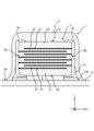
- 2 is a cross-sectional view of the multilayer ceramic capacitor taken along line AA in FIG. 1.
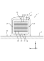
- FIG. 2 is a cross-sectional view of the multilayer ceramic capacitor taken along line BB in FIG. 1.
- FIG. 3 is a cross-sectional view showing an example of a state in which mold resin flows on the upper surface in a molding process of a multilayer ceramic capacitor.
- FIG. 2 is a cross-sectional view showing an example of a state in which mold resin flows on a side surface in a molding process of a multilayer ceramic capacitor.
- FIG. 7 is a cross-sectional view showing another example of a state in which mold resin flows on the side surface in the molding process of a multilayer ceramic capacitor.
- FIG. 3 is a cross-sectional view showing an example of a state in which mold resin flows into a gap in a molding process of a multilayer ceramic capacitor.
- FIG. 7 is a cross-sectional view showing another example of a state in which mold resin flows into a gap in the molding process of a multilayer ceramic capacitor.
- It is a flow chart showing an example of a manufacturing process of a multilayer ceramic capacitor.
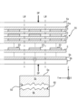
- It is a side view of a laminated sheet showing an example of a pressure bonding process.
- It is a perspective view of a laminated sheet showing an example of a cutting process.
- FIG. 1 is a perspective view showing an example of a multilayer ceramic capacitor 1 mounted on a circuit board 9.
- FIG. 2 is a cross-sectional view of the multilayer ceramic capacitor 1 taken along line AA in FIG.
- FIG. 3 is a cross-sectional view of the multilayer ceramic capacitor 1 taken along the line BB in FIG.
- the multilayer ceramic capacitor 1 is an example of a multilayer ceramic electronic component.
- the multilayer ceramic capacitor 1 includes a multilayer chip 2 having a substantially rectangular parallelepiped shape, and external electrodes 3a and 3b provided on a pair of mutually opposing end surfaces 2A and 2B of the multilayer chip 2.
- the external electrodes 3a and 3b are respectively bonded to a pair of pads 90 on the board surface 9S of the circuit board 9 by solder 8 (see dotted lines).
- the pad 90 is an electrode provided on the plate surface 9S.
- the stacked chip 2 is an example of a stacked body.
- the multilayer ceramic capacitor 1 is mounted on a circuit board 9 while being covered with a molding resin 4 (see dotted line). Thereby, for example, in the multilayer ceramic capacitor 1, the stress caused by bending the circuit board 9 is alleviated, and the moisture resistance is improved.
- the mold resin 4 is an example of a mold material.
- FIGS. 1 to 3 show an X direction, a Y direction, and a Z direction that are orthogonal to each other.
- the X direction is the length (L) direction of the multilayer ceramic capacitor 1, and corresponds to the direction in which the pair of end surfaces 2A and 2B face each other.
- the Y direction is the width (W) direction of the multilayer ceramic capacitor 1, and coincides with the direction in which the pair of side surfaces 2E and 2F face each other.
- the Z direction is the height (H) direction of the multilayer ceramic capacitor 1 and coincides with the stacking direction of the multilayer ceramic capacitor 1.
- the upper and lower surfaces in the stacking direction are referred to as an upper surface 2C and a lower surface 2D.
- the length direction of the multilayer ceramic capacitor 1 is an example of the opposing direction.
- the laminated chip 2 has a laminated structure in which dielectric layers 22 containing a ceramic material functioning as a dielectric and internal electrode layers 23 are alternately laminated.
- the internal electrode layer 23 is mainly composed of base metals such as Ni (nickel), Cu (copper), and Sn (tin).
- base metals such as Ni (nickel), Cu (copper), and Sn (tin).
- noble metals such as Pt (platinum), Pd (palladium), Ag (silver), and Au (gold), or alloys containing these metals may be used.
- the dielectric layer 22 has, for example, a ceramic material having a perovskite structure represented by the general formula ABO3 as a main phase.
- the perovskite structure includes ABO 3- ⁇ that deviates from the stoichiometric composition.
- the ceramic materials include BaTiO 3 (barium titanate), CaZrO 3 (calcium zirconate), CaTiO 3 (calcium titanate), SrTiO 3 (strontium titanate), MgTiO 3 (magnesium titanate), Ba 1- At least one of xy Ca x Sr y Ti 1-z Zr z O 3 (0 ⁇ x ⁇ 1, 0 ⁇ y ⁇ 1, 0 ⁇ z ⁇ 1) can be selected and used.
- Ba 1-x-y Ca x Sry Ti 1-z Zr z O 3 is barium strontium titanate, barium calcium titanate, barium zirconate, barium zirconate titanate, calcium zirconate titanate, and zirconate titanate. Barium calcium, etc.
- the external electrodes 3a and 3b cover mutually opposing end surfaces 2A and 2B of the stacked chip 2, respectively. Moreover, the external electrodes 3a and 3b extend to the upper surface 2C, the lower surface 2D, and the two side surfaces 2E and 2F. However, the external electrodes 3a and 3b are spaced apart from each other on the top surface 2C, bottom surface 2D, and two side surfaces 2E and 2F.
- the external electrodes 3a, 3b are mainly composed of metals such as Cu, Ni, Al (aluminum), Zn (zinc), Au (gold), and Sn (tin), and are made of metals or alloys of two or more of these metals (for example, Cu and Ni), and may further contain ceramics such as a glass component for densifying the external electrodes 3a and 3b and a co-material for controlling the sinterability of the external electrodes 3a and 3b.
- the glass components are oxides such as Ba (barium), Sr (strontium), Ca (calcium), Zn (zinc), Al, Si (silicon), and B (boron).
- the common material is, for example, a ceramic component whose main component is the same material as the main component of the dielectric layer 22.
- a plating layer containing a base metal such as Ni, Cu, or Sn as a main component may be formed on the external electrodes 3a and 3b.
- a layer of conductive resin such as epoxy resin and urethane resin may be formed on the surfaces of the external electrodes 3a and 3b.
- the external electrodes 3a and 3b are formed on a base electrode layer whose main component is Cu that connects to the internal electrodes, a conductive resin layer formed to cover this, and a conductive resin layer formed on the conductive resin layer.
- the layer structure may include a Ni plating layer and a Sn plating layer.
- each internal electrode layer 23 in the length direction are divided into an end surface 2A where the external electrode 3a of the laminated chip 2 is provided and an end surface 2B where the external electrode 3b is provided. alternately exposed.
- each internal electrode layer 23 is alternately electrically connected to the external electrodes 3a and 3b in the stacking direction. That is, the external electrodes 3a, 3b of each end surface 2A, 2B are alternately connected to each internal electrode layer 23 along the stacking direction.
- cover layers 20 and 21 constitute an upper surface 2C and a lower surface 2D of the laminated chip 2, respectively.
- the cover layers 20 and 21 have a ceramic material as a main component, and are formed of the same main component material as the dielectric layer 22.
- the size of the multilayer ceramic capacitor 1 is different between a low-profile type and a high-profile type.
- the height T is the shortest among the height T, length L, and width W of the multilayer chip 2.
- the size of the low-profile multilayer ceramic capacitor 1 has a size relationship of L>W>T or W>L>T.
- the length L, width W, and height T of the low-profile multilayer ceramic capacitor 1 are, for example, 0.6 mm in length, 0.3 mm in width, and 0.20 mm in height, or 1.0 mm in length and 0.2 mm in height. 0.5 mm and height 0.3 mm, or 3.2 mm length, 1.6 mm width, and 1.2 mm height, or 3.2 mm length, 2.5 mm width, and 1.6 mm height. or 4.5 mm in length, 3.2 mm in width, and 2.5 mm in height, but is not limited to these sizes. Further, the numerical values described as sizes each include general tolerances at the time of manufacture, and are not limited to the above numerical values.
- the height T of the multilayer chip 2 is longer than the width (W).
- the size of the high-profile multilayer ceramic capacitor 1 has a size relationship of L>T>W or T>L ⁇ W.
- the high-profile multilayer ceramic capacitor 1 generally has more internal electrode layers 23 than the low-profile multilayer ceramic capacitor 1, and can realize a larger capacitance.
- the length L, width W, and height T of the high-back multilayer ceramic capacitor 1 are, for example, 0.6 mm in length, 0.3 mm in width, and 0.40 mm in height, or 1.0 mm in length and 0.4 mm in height.
- 0.5mm, height 0.7mm, or length 3.2mm, width 1.6mm, height 1.8mm, or length 3.2mm, width 2.5mm, height 3.6mm. or 4.5 mm in length, 3.2 mm in width, and 4.5 mm in height but is not limited to these sizes.
- the numerical values described as sizes each include general tolerances at the time of manufacture, and are not limited to the above numerical values.
- the entire outer surface is covered with molding resin 4 poured from an upper dispenser.
- the viscosity of the mold resin 4 is, for example, 6700 (Pa ⁇ s).
- the circuit board 9 is heated in a batch furnace at 130 to 150 (° C.) for 8 to 10 minutes to harden the mold resin 4.
- the surface roughness Ra of the side surfaces 2E, 2F and the bottom surface 2D of the multilayer chip 2 is set so that the mold resin 4 easily flows into the gap S described above.
- the surface roughness Ra of the upper surface 2C and the lower surface 2D is set to the side surfaces 2E, 2F such that the wettability of the mold resin 4 on the lower surface 2D is greater than that on the side surfaces 2E, 2F.
- the surface roughness is smaller than the surface roughness Ra of .
- the surface roughness Ra is defined in "JIS (Japan Industrial Standards) B 0601 (1994)".
- the upper surface 2C and the lower surface 2D are an example of a pair of first surfaces facing each other, and the side surfaces 2E and 2F are examples of a pair of second surfaces adjacent to the upper surface 2C and the lower surface 2D. Details of the flow of mold resin 4 will be explained below.
- FIG. 4 is a cross-sectional view showing an example of a state in which the mold resin 4 flows on the upper surface 2C in the molding process of the multilayer ceramic capacitor 1.
- components common to those in FIG. 3 are denoted by the same reference numerals, and their explanations will be omitted. Note that in FIGS. 4 to 8, external electrodes 3a, solder 8, and pads 90 are indicated by dotted lines.
- the dispenser 7 that discharges the mold resin 4 is arranged above the multilayer ceramic capacitor 1 so that the discharge port for the mold resin 4 faces the upper surface 2C.
- the mold resin 4 discharged from the dispenser 7 wets and spreads over the upper surface 2C as indicated by the symbol M1.
- FIG. 5 is a cross-sectional view showing an example of a state in which the mold resin 4 flows on the side surfaces 2E and 2F in the molding process of the multilayer ceramic capacitor 1.
- components common to those in FIG. 3 are denoted by the same reference numerals, and their explanations will be omitted.
- the mold resin 4 After the mold resin 4 wets and spreads on the upper surface 2C, it flows downward in the vertical direction along both side surfaces 2E and 2F adjacent to the upper surface 2C according to gravity, as indicated by the symbol M2. At this time, the larger the surface roughness Ra of both side surfaces 2E and 2F, the higher the surface resistance to the mold resin 4. This reduces the wettability of the side surfaces 2E, 2F, making it difficult for the mold resin 4 to flow on the side surfaces 2E, 2F. Therefore, the mold resin 4 flowing from the dispenser 7 along the upper surface 2C has a slow flow rate and tends to accumulate on the side surfaces 2E and 2F.
- the thickness of the molded resin 4 on the side surfaces 2E and 2F in the Y direction is d1 ( ⁇ m).
- FIG. 6 is a cross-sectional view showing another example of the state in which the mold resin 4 flows on the side surfaces 2E and 2F in the molding process of the multilayer ceramic capacitor 1.
- components common to those in FIG. 5 are denoted by the same reference numerals, and their explanations will be omitted.
- the surface resistance to the mold resin 4 is small. This increases the wettability of the side surfaces 2E, 2F, and the mold resin 4 easily flows on the side surfaces 2E, 2F. Therefore, the mold resin 4 flowing from the dispenser 7 along the upper surface 2C has a faster flow rate than in the case of FIG. 5, and is less likely to accumulate on the side surfaces 2E and 2F.
- the thickness of the molded resin 4 on the side surfaces 2E and 2F in the Y direction is d2 ( ⁇ m)
- the thickness d2 is thinner than the thickness d1 in the example of FIG.
- the thicknesses d1 and d2 of the mold resin 4 flowing on the side surfaces 2E and 2F depend on the surface roughness Ra.
- the pressure when the mold resin 4 flows into the gap S between the lower surface 2D and the plate surface 9S of the circuit board 9 is equal to It becomes higher than when d2 is thin. Therefore, when the thickness d1 of the mold resin 4 is large, the mold resin 4 can easily flow into the gap S.
- FIG. 7 is a cross-sectional view showing an example of a state in which the mold resin 4 flows into the gap S in the molding process of the multilayer ceramic capacitor 1.
- the same components as those in FIG. 5 are denoted by the same reference numerals, and the explanation thereof will be omitted.
- the molding resin 4 flows on both side surfaces 2E and 2F as shown in FIG. 5, it flows into the gap S along the lower surface 2D of the stacked chip 2, as shown by the symbol M3.
- the pressure of the inflow of the mold resin 4 is large, and the surface roughness Ra of the lower surface 2D is smaller than the surface roughness Ra of both sides 2E and 2F, so the mold resin 4 easily wets into the gap S. spread. Therefore, voids are less likely to be formed in the mold resin 4 within the gap S, and the reliability of the mold can be improved.
- FIG. 8 is a cross-sectional view showing another example of the state in which the mold resin 4 flows into the gap S in the molding process of the multilayer ceramic capacitor 1.
- components common to those in FIG. 6 are denoted by the same reference numerals, and their explanations will be omitted.
- the surface roughness Ra of the lower surface 2D of the laminated chip 2 is set to the same value as the surface roughness Ra of each side surface 2E, 2F, for example. That is, the surface roughness Ra of the lower surface 2D is larger than that of the example shown in FIG.
- the pressure of the inflow of the mold resin 4 is small and the surface roughness Ra of the lower surface 2D is large, so the mold resin 4 is difficult to wet and spread within the gap S. Therefore, a void P is likely to be formed in the mold resin 4 within the gap S, and there is a possibility that the reliability of the mold may be reduced.
- the mold resin 4 can easily flow into the gap S. Therefore, the formation of a void P in the mold resin 4 within the gap S is suppressed. Therefore, the reliability of the mold of the multilayer ceramic capacitor 1 can be improved.
- the surface roughness Ra of the lower surface 2D is smaller than the surface roughness Ra of both side surfaces 2E and 2F, but may be smaller than the surface roughness Ra of at least one of the side surfaces 2E and 2F. In this case, since the flow into the gap S from at least one of the side surfaces 2E and 2F is facilitated, it is possible to suppress the gap P in the mold resin 4.
- a large stress is likely to occur in the bending direction compared to a high-profile multilayer ceramic capacitor 1. 4 is sufficiently filled, stress is relaxed, so that, for example, the occurrence of cracks can be suppressed.
- the high-profile multilayer ceramic capacitor 1 has more layers than the low-profile multilayer ceramic capacitor 1 and generates more heat, but the gap S must be sufficiently filled with the molding resin 4 as described above. This increases heat dissipation and suppresses temperature rise.
- the difference in surface roughness Ra between the lower surface 2D and the side surfaces 2E and 2F is, for example, 0.025 ( ⁇ m) or more.
- the difference in surface roughness Ra between the bottom surface 2D and the side surfaces 2E, 2F the smaller the difference in appearance between the bottom surface 2D and the side surfaces 2E, 2F. This makes it easier to identify defects such as defects. Therefore, it is preferable that the difference in surface roughness Ra is, for example, 0.151 ( ⁇ m) or less.
- the surface roughness of the lower surface 2D is, for example, 0.041 ( ⁇ m) or more.
- the thickness d1 of the molded resin 4 can be increased as the surface roughness Ra of the side surfaces 2E and 2F increases. Therefore, it is preferable that the surface roughness of the side surfaces 2E and 2F is, for example, 0.090 ( ⁇ m) or more.
- FIG. 9 is a flowchart showing an example of the manufacturing process of the multilayer ceramic capacitor 1. As shown in FIG. This manufacturing process is an example of a method for manufacturing a laminated ceramic electronic component.
- a green sheet forming step St1 is performed.
- a dielectric material obtained by adding various additive compounds (sintering aids, etc.) to ceramic powder is mixed with a binder such as polyvinyl butyral (PVB) resin and an organic solvent such as ethanol or toluene. , plasticizer and wet-mix.
- a dielectric green sheet is coated on a base material by, for example, a die coater method or a doctor blade method, and then dried.
- the base material is, for example, a PET (polyethylene terephthalate) film.
- the additive compounds of the ceramic powder include Mg (magnesium), Mn (manganese), V (vanadium), Cr (chromium), rare earth elements (Y (yttrium), Sm (samarium), Eu (europium), Gd ( oxides of gadolinium), Tb (terbium), Dy (dysprosium), Ho (holmium), Er (erbium), Tm (thulium) and Yb (ytterbium)), as well as Co (cobalt), Ni, Li (lithium) , B (boron), Na (sodium), K (potassium), and Si (silicon) or glass.
- an internal electrode printing step St2 is performed.
- a plurality of internal electrode patterns corresponding to the internal electrode layer 12 are separated from each other by printing a metal conductive paste for forming internal electrodes containing an organic binder on a dielectric green sheet on a base material by gravure printing. to form a film.
- Ceramic particles are added to the metal conductive paste as a co-material.
- the main component of the ceramic particles is not particularly limited, it is preferably the same as the main component ceramic of the dielectric layer 22.
- a lamination step St3 is performed.
- a laminated sheet is formed by laminating dielectric green sheets on which an internal electrode pattern, which will become the internal electrode layer 23, is printed.
- Dielectric green sheets corresponding to the cover layers 20 and 21 are laminated on both end faces of the laminated sheet in the lamination direction.
- a crimping step St4 is performed.
- This step is an example of a step in which a plurality of green sheets each having an internal electrode layer 23 formed on its surface are laminated and pressure-bonded by pressing in the lamination direction with a pressing member.
- a plurality of dielectric green sheets are bonded together by applying pressure to the laminated sheet.
- the compression means include, but are not limited to, a hydrostatic press.
- a cutting step St5 is performed.
- This step is an example of a step of cutting the laminated sheet after pressure bonding along the lamination direction with a blade so as to divide it into a plurality of laminated chips 2.
- a plurality of laminated chips 2 are obtained by cutting the laminated sheet along predetermined cut lines in the lamination direction.
- polishing step St6 a polishing step St6 is performed.
- the stacked chips 2 are polished by, for example, barrel polishing. As a result, the corners of the stacked chip 2 are rounded.
- an external electrode forming step St7 is performed.
- This step is an example of a step of forming a pair of external electrodes 3a, 3b that respectively cover the pair of end faces 2A, 2B of the stacked chip 2 and are alternately connected to the internal electrode layer 23 along the stacking direction.
- a conductive paste containing, for example, metal powder, glass frit, binder, and solvent is applied to each end surface 2A, 2B, upper surface 2C, lower surface 2D, and each side surface 2E, 2F of the laminated chip 2.
- the external electrodes 3a and 3b are formed by drying it. Note that the binder and solvent are evaporated by baking. Examples of the means for applying the conductive paste include a sputtering method and a dipping method.
- a firing step St8 is performed.
- the laminated chip 2 on which the external electrodes 3a and 3b are formed is subjected to binder removal treatment in an N2 atmosphere at 250 to 500°C, and then baked at 1300 to 1400°C for about 1 hour in a reducing atmosphere. , each particle in the laminated chip 2 is sintered. In this manner, the manufacturing process of the multilayer ceramic capacitor 1 is performed.
- metal coating such as Cu, Ni, Sn, etc. may be performed on each of the external electrodes 3a and 3b by plating.
- the external electrode forming step St7 may be performed after the firing step St8.
- the surface roughness Ra of the pressing member that presses the laminated sheet is set so that the surface roughness Ra of the lower surface 2D of the laminated chip 2 is smaller than the surface roughness Ra of the side surfaces 2E and 2F.
- FIG. 10 is a side view of the laminated sheet 5S showing an example of the crimping step St4.
- the laminated sheet 5S includes a plurality of dielectric green sheets 5 having internal electrode layers 12 formed on their surfaces, and dielectric green sheets 5a and 5b corresponding to cover layers 20 and 21.
- a plurality of dielectric green sheets 5 are stacked adjacent to each other in the stacking direction, and dielectric green sheets 5a and 5b are stacked on the top and bottom dielectric green sheets 5, respectively, in the stacking direction.
- the laminated sheet 5S is cut into individual laminated chips 2 along the cutting line LW in the cutting step St5.
- the laminated sheet 5S is pressed by being sandwiched between a pair of pressing members 6a and 6b from above and below in the lamination direction.
- the pressing members 6a and 6b are, for example, metal plate-like members, and press the laminated sheet 5S from above and below in the lamination direction by, for example, hydrostatic pressure, as indicated by the symbol DP.
- the symbol Ga shows an enlarged view of the surface 60 of the lower pressing member 6b and the lower surface 50 of the dielectric green sheet 5b that come into contact with each other in the crimping step St4.
- the surface 60 of the pressing member 6b is provided with irregularities corresponding to the designed value of the surface roughness Ra of the lower surface 2D of the laminated chip 2.
- the unevenness of the pressing member 6b is transferred to the lower surface 50 of the dielectric green sheet 5b by the pressing member 6b pressing the dielectric green sheet 5b in the pressing step St4.
- the surface roughness Ra of the lower surface 2D of the laminated chip 2 corresponding to the lower surface 50 becomes a desired value smaller than the surface roughness Ra of the side surfaces 2E and 2F.
- the surface roughness Ra of the surface of the pressing member 6b that contacts the lower surface 2D is set so that the surface roughness Ra of the lower surface 2D is smaller than the surface roughness Ra of the side surfaces 2E and 2F.
- the 2D surface roughness Ra can be easily adjusted to a desired value.
- the surface roughness Ra of the lower surface 2D of the laminated chip 2 is mentioned, but the surface roughness Ra of the upper surface 2C can also be adjusted by the same means as described above.
- the surface roughness Ra of the pressing member 6a that contacts the upper dielectric green sheet 5a is set according to the desired value of the upper surface 2C.
- the unevenness of the pressing member 6a is transferred to the upper surface of the dielectric green sheet 5a, and the surface roughness Ra of the upper surface 2C becomes smaller than the surface roughness Ra of the side surfaces 2E and 2F.
- the adjustment of the surface roughness Ra of the lower surface 2D is not limited to the above-mentioned means.
- irregularities may be formed on the cutting edge of the blade so that the surface roughness Ra of the lower surface 2D of the stacked chip 2 is smaller than the surface roughness Ra of the side surfaces 2E and 2F.
- FIG. 11 is a perspective view of the laminated sheet 5S showing an example of the cutting step St5.
- the laminated sheet 5S is cut in the lamination direction along the cutting line LW by a rotating disc-shaped blade BL. Thereby, a plurality of laminated chips 2 are obtained.
- the symbol Gb shows an enlarged part of the cutting edge BLa of the blade BL.
- a saw-like unevenness is formed on the cutting edge BLa.
- the uneven shape of the cutting edge BLa is determined according to a desired value of the surface roughness Ra of the side surfaces 2E and 2F of the laminated chip 2.
- the height, pitch, etc. of the unevenness of the cutting edge BLa are determined so as to roughen the cut surface of the laminated sheet 5S corresponding to the side surfaces 2E and 2F.
- the surface roughness Ra of the lower surface 2D of the laminated chip 2 becomes smaller than the surface roughness Ra of the side surfaces 2E and 2F.
- the surface roughness Ra of the side surfaces 2E and 2F is can be easily adjusted to the desired value.
- the surface roughness Ra of the side surfaces 2E and 2F is adjusted, but only the surface roughness Ra of one of the side surfaces 2E and 2F may be adjusted.
- the surface roughness Ra of the side surfaces 2E and 2F is adjusted to be larger than the surface roughness Ra of the bottom surface 2D, but the surface roughness Ra of the bottom surface 2D and the surface roughness of the top surface 2C are It may be adjusted so that it is larger than both Ra.
- Table 1 shows the evaluation results of the multilayer ceramic capacitors of Examples 1 to 6 and Comparative Examples 1 and 2 (hereinafter referred to as Comparative Examples 1 and 2).
- Multilayer ceramic capacitors of Examples 1 to 6 and Comparative Examples 1 and 2 were manufactured according to the above manufacturing process and evaluated.
- each multilayer ceramic capacitor is of a high-profile type.
- the size of each multilayer ceramic capacitor is 0.6 (mm) in length, 0.3 (mm) in width, and 0.4 (mm) in height, and the rated voltage of each multilayer ceramic capacitor is 6.3 (V). did.
- the surface roughness Ra of each multilayer ceramic capacitor was adjusted in the above-mentioned crimping step St4.
- the surface roughness Ra of the bottom surface 2D and the side surfaces 2E and 2F was set to 0.065 ( ⁇ m) and 0.09 ( ⁇ m), respectively.
- the surface roughness Ra of the bottom surface 2D and the side surfaces 2E, 2F were set to 0.073 ( ⁇ m) and 0.129 ( ⁇ m), respectively.
- the surface roughness Ra of the bottom surface 2D and the side surfaces 2E, 2F were set to 0.041 ( ⁇ m) and 0.192 ( ⁇ m), respectively.
- the surface roughness Ra of the bottom surface 2D and the side surfaces 2E and 2F was set to 0.054 ( ⁇ m) and 0.116 ( ⁇ m), respectively.
- the surface roughness Ra of the lower surface 2D and the side surfaces 2E, 2F was set to 0.062 ( ⁇ m) and 0.091 ( ⁇ m), respectively.
- the surface roughness Ra of the bottom surface 2D and the side surfaces 2E, 2F were set to 0.048 ( ⁇ m) and 0.127 ( ⁇ m), respectively.
- the differences ⁇ Ra between the surface roughness Ra of the lower surface 2D of Examples 1 to 6 and the surface roughness Ra of the side surfaces 2E and 2F are 0.025 ( ⁇ m), 0.056 ( ⁇ m), and 0.0. They were 151 ( ⁇ m), 0.062 ( ⁇ m), 0.029 ( ⁇ m), and 0.079 ( ⁇ m).
- the surface roughness Ra of the bottom surface 2D was set to be smaller than the surface roughness Ra of each of the side surfaces 2E and 2F.
- the surface roughness Ra of the bottom surface 2D and the side surfaces 2E, 2F were set to 0.089 ( ⁇ m) and 0.068 ( ⁇ m), respectively.
- the surface roughness Ra of the bottom surface 2D and the side surfaces 2E, 2F were set to 0.075 ( ⁇ m) and 0.061 ( ⁇ m), respectively.
- the difference ⁇ Ra between the surface roughness Ra of the lower surface 2D and the surface roughness Ra of the side surfaces 2E and 2F of Comparative Examples 1 and 2 was ⁇ 0.021 ( ⁇ m) and ⁇ 0.014, respectively.
- the surface roughness Ra of the bottom surface 2D was set to be larger than the surface roughness Ra of each of the side surfaces 2E and 2F.
- the multilayer ceramic capacitors of Examples 1 to 6 and Comparative Examples 1 and 2 were mounted on the circuit board 9 by a reflow process so that the lower surface 2D faced the plate surface 9S.
- molding resin was poured into the multilayer ceramic capacitor from a dispenser above the circuit board 9 to cover the entire outer surface of the capacitor.
- the viscosity of the mold resin at this time was 6700 (Pa ⁇ s).
- the circuit board 9 was heated in a batch furnace at 130 to 150 (°C) for 8 to 10 minutes to harden the mold resin.
- the mold resin was cured, the presence or absence of voids in the mold resin filled in the gap between the lower surface 2D and the plate surface 9S was confirmed by a cross-sectional view taken along the line AA in FIG.
- the determination result of the comparative example was set as "NG". This is because the surface roughness Ra of the lower surface 2D is larger than the surface roughness Ra of the side surfaces 2E and 2F in Examples 1 to 6, so that the mold resin spreads from the side surfaces 2E and 2F along the lower surface 2D into voids as described above. This is because it is difficult to flow into the
- the mold resin 4 flows suitably into the gap.
- the surface roughness Ra of the lower surface 2D is 0.041 to 0.065 ( ⁇ m) and the surface roughness Ra of the side surfaces 2E and 2F is 0.090 to 0.192 ( ⁇ m)
- mold resin is suitable. It is preferable because it flows into the gap.
- Multilayer ceramic capacitor Multilayer chip 2A, 2B End surface 2C Top surface 2D Bottom surface 2E, 2F Side surface 3a, 3b External electrode 4 Mold resin 5, 5a, 5b Dielectric green sheet 6a, 6b Pressing member 9 Circuit board 20, 21 Cover layer 22 Dielectric layer 23 Internal electrode layer BL Blade
Landscapes
- Engineering & Computer Science (AREA)
- Power Engineering (AREA)
- Microelectronics & Electronic Packaging (AREA)
- Manufacturing & Machinery (AREA)
- Chemical & Material Sciences (AREA)
- Ceramic Engineering (AREA)
- Inorganic Chemistry (AREA)
- Ceramic Capacitors (AREA)
- Fixed Capacitors And Capacitor Manufacturing Machines (AREA)
Priority Applications (2)
| Application Number | Priority Date | Filing Date | Title |
|---|---|---|---|
| JP2024545462A JPWO2024053230A1 (https=) | 2022-09-05 | 2023-07-05 | |
| US18/806,106 US20240412924A1 (en) | 2022-09-05 | 2024-08-15 | Multilayer ceramic electronic device, manufacturing method of the same, and circuit board |
Applications Claiming Priority (2)
| Application Number | Priority Date | Filing Date | Title |
|---|---|---|---|
| JP2022140865 | 2022-09-05 | ||
| JP2022-140865 | 2022-09-05 |
Related Child Applications (1)
| Application Number | Title | Priority Date | Filing Date |
|---|---|---|---|
| US18/806,106 Continuation US20240412924A1 (en) | 2022-09-05 | 2024-08-15 | Multilayer ceramic electronic device, manufacturing method of the same, and circuit board |
Publications (1)
| Publication Number | Publication Date |
|---|---|
| WO2024053230A1 true WO2024053230A1 (ja) | 2024-03-14 |
Family
ID=90192338
Family Applications (1)
| Application Number | Title | Priority Date | Filing Date |
|---|---|---|---|
| PCT/JP2023/024974 Ceased WO2024053230A1 (ja) | 2022-09-05 | 2023-07-05 | 積層セラミック電子部品、その製造方法、及び回路基板 |
Country Status (3)
| Country | Link |
|---|---|
| US (1) | US20240412924A1 (https=) |
| JP (1) | JPWO2024053230A1 (https=) |
| WO (1) | WO2024053230A1 (https=) |
Citations (4)
| Publication number | Priority date | Publication date | Assignee | Title |
|---|---|---|---|---|
| JPH09260204A (ja) * | 1996-03-25 | 1997-10-03 | Taiyo Yuden Co Ltd | 積層コンデンサ |
| JP2009176771A (ja) * | 2008-01-21 | 2009-08-06 | Tdk Corp | 積層セラミック電子部品、積層セラミック電子部品の製造方法、及びセラミック素体の不良選別方法 |
| JP2016092289A (ja) * | 2014-11-07 | 2016-05-23 | 株式会社村田製作所 | コンデンサ素子の実装構造体 |
| JP2018046131A (ja) * | 2016-09-14 | 2018-03-22 | 太陽誘電株式会社 | 積層セラミックコンデンサ |
Family Cites Families (10)
| Publication number | Priority date | Publication date | Assignee | Title |
|---|---|---|---|---|
| JP2017037930A (ja) * | 2015-08-07 | 2017-02-16 | 株式会社村田製作所 | セラミック電子部品の製造方法及びセラミック電子部品 |
| US10143087B2 (en) * | 2016-05-18 | 2018-11-27 | Murata Manufacturing Co., Ltd. | Capacitor element-mounted structure |
| JP7125093B2 (ja) * | 2018-04-11 | 2022-08-24 | 太陽誘電株式会社 | 積層セラミックコンデンサ及びその製造方法 |
| JP7510741B2 (ja) * | 2018-08-23 | 2024-07-04 | 太陽誘電株式会社 | 積層セラミック電子部品の製造方法 |
| KR102185055B1 (ko) * | 2018-10-02 | 2020-12-01 | 삼성전기주식회사 | 적층 세라믹 전자부품 |
| JP7629280B2 (ja) * | 2020-07-16 | 2025-02-13 | 太陽誘電株式会社 | セラミック電子部品およびその製造方法 |
| JP7536620B2 (ja) * | 2020-11-27 | 2024-08-20 | 太陽誘電株式会社 | セラミック電子部品、実装基板およびセラミック電子部品の製造方法 |
| JP7611683B2 (ja) * | 2020-12-07 | 2025-01-10 | 太陽誘電株式会社 | セラミック電子部品、実装基板およびセラミック電子部品の製造方法 |
| JP7544157B2 (ja) * | 2021-02-02 | 2024-09-03 | 株式会社村田製作所 | 無機粒子含有ペースト、無機粒子含有膜、及び積層体 |
| JP7818216B2 (ja) * | 2021-11-11 | 2026-02-20 | パナソニックIpマネジメント株式会社 | 積層バリスタ及びその製造方法 |
-
2023
- 2023-07-05 JP JP2024545462A patent/JPWO2024053230A1/ja active Pending
- 2023-07-05 WO PCT/JP2023/024974 patent/WO2024053230A1/ja not_active Ceased
-
2024
- 2024-08-15 US US18/806,106 patent/US20240412924A1/en active Pending
Patent Citations (4)
| Publication number | Priority date | Publication date | Assignee | Title |
|---|---|---|---|---|
| JPH09260204A (ja) * | 1996-03-25 | 1997-10-03 | Taiyo Yuden Co Ltd | 積層コンデンサ |
| JP2009176771A (ja) * | 2008-01-21 | 2009-08-06 | Tdk Corp | 積層セラミック電子部品、積層セラミック電子部品の製造方法、及びセラミック素体の不良選別方法 |
| JP2016092289A (ja) * | 2014-11-07 | 2016-05-23 | 株式会社村田製作所 | コンデンサ素子の実装構造体 |
| JP2018046131A (ja) * | 2016-09-14 | 2018-03-22 | 太陽誘電株式会社 | 積層セラミックコンデンサ |
Also Published As
| Publication number | Publication date |
|---|---|
| JPWO2024053230A1 (https=) | 2024-03-14 |
| US20240412924A1 (en) | 2024-12-12 |
Similar Documents
| Publication | Publication Date | Title |
|---|---|---|
| CN109920644B (zh) | 陶瓷电子器件及陶瓷电子器件的制造方法 | |
| JP2025170129A (ja) | 積層セラミックコンデンサ | |
| JP7562249B2 (ja) | セラミック電子部品およびその製造方法 | |
| JP7651263B2 (ja) | 積層セラミックコンデンサおよびその製造方法 | |
| JP2018022833A (ja) | 電子部品 | |
| CN116544034A (zh) | 陶瓷电子部件及其制造方法 | |
| JP2000243650A (ja) | 積層セラミックコンデンサおよびその製造方法 | |
| WO2024053230A1 (ja) | 積層セラミック電子部品、その製造方法、及び回路基板 | |
| CN115732229A (zh) | 陶瓷电子器件及其制造方法 | |
| JP7843151B2 (ja) | セラミック電子部品及びその製造方法 | |
| WO2024105975A1 (ja) | 積層セラミック電子部品及びその製造方法 | |
| US20260100311A1 (en) | Method for manufacturing multilayer ceramic electronic component and multilayer ceramic electronic component | |
| JP7633788B2 (ja) | セラミック電子部品およびその製造方法 | |
| WO2024014099A1 (ja) | セラミック電子部品及びその製造方法 | |
| JP2024044676A (ja) | 積層セラミック電子部品 | |
| US20250357047A1 (en) | Multilayer ceramic electronic component and method of manufacturing the same | |
| JP2025110767A (ja) | 積層セラミック電子部品及びその製造方法 | |
| WO2024180930A1 (ja) | 積層セラミック電子部品及びその製造方法 | |
| WO2025105376A1 (ja) | 積層セラミック電子部品及びその製造方法 | |
| JP2025110776A (ja) | 積層セラミック電子部品及びその製造方法 | |
| JP2025056651A (ja) | 積層セラミック電子部品 | |
| JP2024146173A (ja) | 積層セラミック電子部品 | |
| WO2024190120A1 (ja) | 積層セラミック電子部品、電子装置、及び積層セラミック電子部品の製造方法 | |
| WO2024079966A1 (ja) | 積層セラミック電子部品 | |
| JP2024136218A (ja) | 積層セラミック電子部品、回路基板、電子部品包装体、及び積層セラミック電子部品の製造方法 |
Legal Events
| Date | Code | Title | Description |
|---|---|---|---|
| 121 | Ep: the epo has been informed by wipo that ep was designated in this application |
Ref document number: 23862775 Country of ref document: EP Kind code of ref document: A1 |
|
| WWE | Wipo information: entry into national phase |
Ref document number: 2024545462 Country of ref document: JP |
|
| NENP | Non-entry into the national phase |
Ref country code: DE |
|
| 122 | Ep: pct application non-entry in european phase |
Ref document number: 23862775 Country of ref document: EP Kind code of ref document: A1 |