WO2024048301A1 - Élément de détection de lumière et dispositif électronique - Google Patents
Élément de détection de lumière et dispositif électronique Download PDFInfo
- Publication number
- WO2024048301A1 WO2024048301A1 PCT/JP2023/029717 JP2023029717W WO2024048301A1 WO 2024048301 A1 WO2024048301 A1 WO 2024048301A1 JP 2023029717 W JP2023029717 W JP 2023029717W WO 2024048301 A1 WO2024048301 A1 WO 2024048301A1
- Authority
- WO
- WIPO (PCT)
- Prior art keywords
- transistor
- gate electrode
- pixels
- transistors
- photoelectric conversion
- Prior art date
Links
- 238000001514 detection method Methods 0.000 title abstract description 26
- 238000006243 chemical reaction Methods 0.000 claims abstract description 87
- 238000000926 separation method Methods 0.000 claims abstract description 58
- 238000009792 diffusion process Methods 0.000 claims description 44
- 238000007667 floating Methods 0.000 claims description 44
- 239000003990 capacitor Substances 0.000 claims description 22
- 238000007599 discharging Methods 0.000 claims description 6
- 229910052751 metal Inorganic materials 0.000 claims description 6
- 239000002184 metal Substances 0.000 claims description 6
- 238000003384 imaging method Methods 0.000 description 43
- 238000012545 processing Methods 0.000 description 36
- 238000010586 diagram Methods 0.000 description 20
- 230000000875 corresponding effect Effects 0.000 description 13
- 238000005516 engineering process Methods 0.000 description 13
- 238000000034 method Methods 0.000 description 13
- 238000002955 isolation Methods 0.000 description 7
- 102100036285 25-hydroxyvitamin D-1 alpha hydroxylase, mitochondrial Human genes 0.000 description 6
- 101000875403 Homo sapiens 25-hydroxyvitamin D-1 alpha hydroxylase, mitochondrial Proteins 0.000 description 6
- 101100099196 Saccharomyces cerevisiae (strain ATCC 204508 / S288c) TGL2 gene Proteins 0.000 description 6
- 238000012546 transfer Methods 0.000 description 6
- 230000007246 mechanism Effects 0.000 description 5
- 230000008569 process Effects 0.000 description 5
- 230000007423 decrease Effects 0.000 description 4
- 230000008859 change Effects 0.000 description 3
- 230000000694 effects Effects 0.000 description 3
- 239000012212 insulator Substances 0.000 description 3
- 230000002093 peripheral effect Effects 0.000 description 3
- 239000000758 substrate Substances 0.000 description 3
- VYPSYNLAJGMNEJ-UHFFFAOYSA-N Silicium dioxide Chemical compound O=[Si]=O VYPSYNLAJGMNEJ-UHFFFAOYSA-N 0.000 description 2
- 230000005540 biological transmission Effects 0.000 description 2
- 230000001276 controlling effect Effects 0.000 description 2
- 239000010949 copper Substances 0.000 description 2
- 238000013461 design Methods 0.000 description 2
- 239000010931 gold Substances 0.000 description 2
- 238000009434 installation Methods 0.000 description 2
- 230000010354 integration Effects 0.000 description 2
- 230000003287 optical effect Effects 0.000 description 2
- TWNQGVIAIRXVLR-UHFFFAOYSA-N oxo(oxoalumanyloxy)alumane Chemical compound O=[Al]O[Al]=O TWNQGVIAIRXVLR-UHFFFAOYSA-N 0.000 description 2
- BPUBBGLMJRNUCC-UHFFFAOYSA-N oxygen(2-);tantalum(5+) Chemical compound [O-2].[O-2].[O-2].[O-2].[O-2].[Ta+5].[Ta+5] BPUBBGLMJRNUCC-UHFFFAOYSA-N 0.000 description 2
- 238000005070 sampling Methods 0.000 description 2
- 239000004065 semiconductor Substances 0.000 description 2
- 230000035945 sensitivity Effects 0.000 description 2
- 229910052814 silicon oxide Inorganic materials 0.000 description 2
- 239000002356 single layer Substances 0.000 description 2
- 229910018072 Al 2 O 3 Inorganic materials 0.000 description 1
- RYGMFSIKBFXOCR-UHFFFAOYSA-N Copper Chemical compound [Cu] RYGMFSIKBFXOCR-UHFFFAOYSA-N 0.000 description 1
- 229910004298 SiO 2 Inorganic materials 0.000 description 1
- BQCADISMDOOEFD-UHFFFAOYSA-N Silver Chemical compound [Ag] BQCADISMDOOEFD-UHFFFAOYSA-N 0.000 description 1
- 230000001133 acceleration Effects 0.000 description 1
- 229910052782 aluminium Inorganic materials 0.000 description 1
- XAGFODPZIPBFFR-UHFFFAOYSA-N aluminium Chemical compound [Al] XAGFODPZIPBFFR-UHFFFAOYSA-N 0.000 description 1
- 230000003321 amplification Effects 0.000 description 1
- 239000003086 colorant Substances 0.000 description 1
- 238000002485 combustion reaction Methods 0.000 description 1
- 238000004891 communication Methods 0.000 description 1
- 229910052802 copper Inorganic materials 0.000 description 1
- 230000002596 correlated effect Effects 0.000 description 1
- 239000000428 dust Substances 0.000 description 1
- 230000004313 glare Effects 0.000 description 1
- PCHJSUWPFVWCPO-UHFFFAOYSA-N gold Chemical compound [Au] PCHJSUWPFVWCPO-UHFFFAOYSA-N 0.000 description 1
- 229910052737 gold Inorganic materials 0.000 description 1
- 229910000449 hafnium oxide Inorganic materials 0.000 description 1
- WIHZLLGSGQNAGK-UHFFFAOYSA-N hafnium(4+);oxygen(2-) Chemical compound [O-2].[O-2].[Hf+4] WIHZLLGSGQNAGK-UHFFFAOYSA-N 0.000 description 1
- CJNBYAVZURUTKZ-UHFFFAOYSA-N hafnium(iv) oxide Chemical compound O=[Hf]=O CJNBYAVZURUTKZ-UHFFFAOYSA-N 0.000 description 1
- 238000012423 maintenance Methods 0.000 description 1
- 239000000463 material Substances 0.000 description 1
- 238000005259 measurement Methods 0.000 description 1
- 230000000116 mitigating effect Effects 0.000 description 1
- 238000012986 modification Methods 0.000 description 1
- 230000004048 modification Effects 0.000 description 1
- 238000003199 nucleic acid amplification method Methods 0.000 description 1
- 230000001151 other effect Effects 0.000 description 1
- 238000005192 partition Methods 0.000 description 1
- 229910021420 polycrystalline silicon Inorganic materials 0.000 description 1
- 229920006395 saturated elastomer Polymers 0.000 description 1
- 230000035939 shock Effects 0.000 description 1
- 229910052710 silicon Inorganic materials 0.000 description 1
- 239000010703 silicon Substances 0.000 description 1
- 229910052709 silver Inorganic materials 0.000 description 1
- 239000004332 silver Substances 0.000 description 1
- 229910052715 tantalum Inorganic materials 0.000 description 1
- GUVRBAGPIYLISA-UHFFFAOYSA-N tantalum atom Chemical compound [Ta] GUVRBAGPIYLISA-UHFFFAOYSA-N 0.000 description 1
- 229910001936 tantalum oxide Inorganic materials 0.000 description 1
- 230000002123 temporal effect Effects 0.000 description 1
- 239000011800 void material Substances 0.000 description 1
Images


Classifications
-
- H—ELECTRICITY
- H01—ELECTRIC ELEMENTS
- H01L—SEMICONDUCTOR DEVICES NOT COVERED BY CLASS H10
- H01L27/00—Devices consisting of a plurality of semiconductor or other solid-state components formed in or on a common substrate
- H01L27/14—Devices consisting of a plurality of semiconductor or other solid-state components formed in or on a common substrate including semiconductor components sensitive to infrared radiation, light, electromagnetic radiation of shorter wavelength or corpuscular radiation and specially adapted either for the conversion of the energy of such radiation into electrical energy or for the control of electrical energy by such radiation
- H01L27/144—Devices controlled by radiation
- H01L27/146—Imager structures
-
- H—ELECTRICITY
- H04—ELECTRIC COMMUNICATION TECHNIQUE
- H04N—PICTORIAL COMMUNICATION, e.g. TELEVISION
- H04N25/00—Circuitry of solid-state image sensors [SSIS]; Control thereof
- H04N25/70—SSIS architectures; Circuits associated therewith
-
- H—ELECTRICITY
- H04—ELECTRIC COMMUNICATION TECHNIQUE
- H04N—PICTORIAL COMMUNICATION, e.g. TELEVISION
- H04N25/00—Circuitry of solid-state image sensors [SSIS]; Control thereof
- H04N25/70—SSIS architectures; Circuits associated therewith
- H04N25/76—Addressed sensors, e.g. MOS or CMOS sensors
- H04N25/77—Pixel circuitry, e.g. memories, A/D converters, pixel amplifiers, shared circuits or shared components
- H04N25/771—Pixel circuitry, e.g. memories, A/D converters, pixel amplifiers, shared circuits or shared components comprising storage means other than floating diffusion
Definitions
- the present disclosure relates to a photodetector and an electronic device.
- Patent Document 1 discloses an imaging device including a separation section that separates adjacent pixels.
- the presence of the separation portion limits the arrangement of photoelectric conversion elements and transistors within the pixel, reducing layout efficiency.
- One aspect of the present disclosure improves layout efficiency.
- a photodetection element includes a plurality of pixels arranged in a plane direction, and a direction that intersects the plane direction between adjacent pixels so as to separate adjacent pixels among the plurality of pixels.
- a separating section extending in a direction in which each of the plurality of pixels includes a photoelectric conversion element and a plurality of transistors;
- the gate electrodes of the transistors are disposed on opposite sides of the isolation section and are connected to each other across the isolation section.
- An electronic device includes a photodetection element, and the photodetection element includes a plurality of pixels arranged in a planar direction, and a plurality of pixels that are adjacent to each other so as to separate adjacent pixels among the plurality of pixels. a separation portion extending in a direction intersecting the plane direction between matching pixels, each of the plurality of pixels includes a photoelectric conversion element and a plurality of transistors, and when viewed in plan, adjacent pixels The gate electrodes of specific transistors among the plurality of transistors of each pixel are arranged on opposite sides of the separation section, and are connected to each other across the separation section.
- FIG. 1 is a diagram illustrating an example of a schematic configuration of an electronic device including a photodetection element according to an embodiment.
- FIG. 2 is a circuit diagram showing an example of a schematic configuration of a pixel.
- FIG. 3 is a diagram illustrating an example of pixel operation. It is a figure showing the 1st example of composition of a photodetection element. It is a figure showing the 1st example of composition of a photodetection element. It is a figure showing the 1st example of composition of a photodetection element. It is a figure showing the 2nd example of composition of a photodetection element. It is a figure which shows the 2nd structural example of a photodetection element.
- FIG. 1 is a block diagram showing an example of a schematic configuration of a vehicle control system.
- FIG. 2 is an explanatory diagram showing an example of installation positions of an outside-vehicle information detection section and an imaging section.
- CMOS image sensors (CMOS-type solid-state imaging devices) and the like are known as devices and electronic devices that include photodetecting elements. With the miniaturization technology associated with the CMOS process, it is possible to easily create an active structure with an amplification function for each pixel. Furthermore, a peripheral circuit section such as a signal processing circuit that processes signals output from each pixel of the pixel array section can be integrated on the same chip (substrate) as the pixel array section. Many technologies related to CMOS image sensors have been proposed.
- LOFIC Lateral Overflow Integration Capacitor
- a capacitor is provided within a pixel to directly increase the amount of charge handled.
- one pixel includes photoelectric conversion elements of different sizes with different light-receiving sensitivities.
- a global shutter technique is also known, as disclosed in Patent Document 1, in which exposure is started for all pixels at the same time and exposure is ended for all pixels at the same time.
- a deep insulator such as DTI (Deep Trench Isolation) is sometimes provided as an isolation part.
- DTI Deep Trench Isolation
- the presence of the isolation section surrounding the pixels limits the placement of photoelectric conversion elements and transistors, reducing layout efficiency.
- the gate electrode is placed apart from the isolation part to avoid the risk of short circuits.
- the size of the transistor becomes smaller, which may cause a decrease in the amount of saturated signal, a transfer problem, etc.
- Such problems become more apparent as the number of elements such as transistors increases as pixels become smaller and more sophisticated.
- the elements of adjacent pixels are arranged symmetrically, for example, with the separation section in between.
- transistors located near the separation portion share a gate electrode. This eliminates wasted space and improves layout efficiency.
- FIG. 1 is a diagram illustrating an example of a schematic configuration of an electronic device including a photodetection element according to an embodiment.
- the illustrated electronic device 100 is a CMOS image sensor, and includes a pixel array section 1 and a peripheral section. These elements are formed on a semiconductor substrate, such as silicon.
- a vertical drive section 5 As peripheral parts, in FIG. 1, a vertical drive section 5, a column signal processing section 6, a horizontal drive section 7, a signal processing section 8, and a system control section 9 are illustrated.
- FIG. 1 also shows an XYZ coordinate system for the pixel array section 1.
- the X-axis direction is also referred to as a horizontal direction (lateral direction) or the like.
- the Y-axis direction is also referred to as a vertical direction (longitudinal direction) or the like.
- the Z-axis direction is a direction perpendicular to the XY plane direction, and corresponds to, for example, the thickness direction of the semiconductor substrate.
- the pixel array section 1 includes a plurality of pixels 2.
- the plurality of pixels 2 are two-dimensionally arranged in the X-axis direction and the Y-axis direction.
- Each pixel 2 generates and outputs a voltage signal according to the amount of received light. This signal is also called a pixel signal.
- the photodetecting element 3 includes at least two adjacent pixels among the plurality of pixels 2. As long as there is no contradiction, the light detection element 3 and the plurality of pixels 2 may be read as appropriate.
- the vertical drive section 5 drives the plurality of pixels 2 of the pixel array section 1, for example, all at the same time or for each pixel row. Driving includes selective scanning of the plurality of pixels 2 row by row in order to read out pixel signals. The pixel signal of the selectively scanned pixel 2 is sent to the column signal processing section 6.
- the vertical drive unit 5 is connected to the pixel array unit 1 via a plurality of control lines HL, for example, for each pixel row.
- Each control line HL extends in the row direction and connects each pixel 2 of the corresponding pixel row to the vertical drive unit 5.
- the vertical drive unit 5 includes, for example, a shift register, an address decoder, and the like.
- being connected may be understood to mean being electrically connected.
- Being electrically connected may include being connected with another element interposed therebetween, as long as the functions of the connected elements are not hindered.
- the column signal processing unit 6 processes pixel signals from each pixel 2 in the row selected by the vertical drive unit 5 for each pixel column.
- the column signal processing section 6 includes a plurality of unit circuits corresponding to pixel columns.
- the processing by the column signal processing unit 6 includes noise removal processing, CDS (Correlated Double Sampling) processing, DDS (Double Data Sampling) processing, A/D (Analog/Digital) conversion processing of analog pixel signals, etc. include.
- the pixel signal is digitized and sent to the signal processing section 8.
- the column signal processing section 6 is connected to the pixel array section 1 via a plurality of signal lines VL. Each signal line VL extends in the column direction and connects each pixel 2 of the corresponding pixel column to the column signal processing unit 6.
- the column signal processing section 6 includes, for example, a shift register, an address decoder, and the like.
- the horizontal drive unit 7 sequentially selects the unit circuits of the column signal processing unit 6. Due to this selective scanning by the horizontal driving section 7, pixel signals for each pixel column processed by the column signal processing section 6 are sequentially output to the signal processing section 8.
- the horizontal drive unit 7 includes, for example, a shift register, an address decoder, and the like.
- the signal processing unit 8 processes the pixel signals from the column signal processing unit 6, generates and outputs an image signal based on the pixel signals. Note that the most necessary data for processing may be temporarily stored, for example, in a storage unit (not shown).
- the system control section 9 controls the vertical drive section 5, column signal processing section 6, and horizontal drive section 7.
- the system control unit 9 is configured to include a timing generator and the like to generate various timing signals and supply them to corresponding parts.
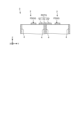
- the pixel 2 of the pixel array section 1 will be explained with reference to FIG. 2 as well.
- FIG. 2 is a circuit diagram showing an example of a schematic configuration of a pixel.
- the pixel 2 includes a photoelectric conversion element PD, a floating diffusion FD, a capacitor FC, and a plurality of transistors.
- the plurality of transistors include a transistor TGL, a transistor FDG, a transistor FCG, a transistor OFG, a transistor RST, a transistor AMP, and a transistor SEL.
- the illustrated transistor is a FET, and has a drain and a source that are current terminals, and a gate electrode that is a control terminal. Unless otherwise specified, when a transistor is connected between two elements, it means that one current terminal (drain or source) of the transistor is connected to one element, and the other current terminal of the transistor is connected to the other element. shall mean that the current terminal is connected.
- the gate electrode of the transistor TGL is shown as a gate electrode TGLG.
- the gate electrode of the transistor FDG is illustrated as a gate electrode FDGG.
- the gate electrode of transistor FCG is shown as gate electrode FCGG.
- the gate electrode of the transistor OFG is shown as a gate electrode OFGG.
- the gate electrode of the transistor RST is shown as a gate electrode RSTG.
- the gate electrode of the transistor AMP is illustrated as a gate electrode AMPG.
- the gate electrode of the transistor SEL is shown as a gate electrode SELG. Note that the gate of the transistor AMP is connected to the floating diffusion FD.
- control line HL_TGL the control line HL connected to the gate electrode TGLG of the transistor TGL is referred to as a control line HL_TGL and illustrated.
- the control line HL connected to the gate electrode FDGG of the transistor FDG is illustrated as a control line HL_FDG.
- the control line HL connected to the gate electrode FCGG of the transistor FCG is shown as a control line HL_FCG.
- the control line HL connected to the gate electrode OFGG of the transistor OFG is illustrated as a control line HL_OFG.
- the control line HL connected to the gate electrode RSTG of the transistor RST is shown as a control line HL_RST.
- the control line HL connected to the gate electrode SELG of the transistor SEL is shown as a control line HL_SEL.
- the on/off state (conductive state and non-conductive state) of each transistor is controlled by a control signal from the corresponding control line HL.
- the photoelectric conversion element PD generates and accumulates charges according to the amount of received light.
- An example of the photoelectric conversion element PD is a photodiode or the like.
- the transistor TGL is a transfer transistor for transferring the charge of the photoelectric conversion element PD to the floating diffusion FD.
- Transistor TGL is connected between photoelectric conversion element PD and floating diffusion FD.
- the floating diffusion FD accumulates the charge from the photoelectric conversion element PD transferred via the transfer transistor TGL and converts it into a voltage. A voltage is generated according to the amount of accumulated charge.
- the floating diffusion FD is formed to have a floating diffusion capacitance between at least the transistor TGL, the transistor AMP, and the transistor FDG.
- the transistor FDG is a conversion efficiency switching transistor that switches the conversion efficiency from charge to voltage in the floating diffusion FD.
- Transistor FDG is connected between floating diffusion FD, transistor RST, and transistor FCG.
- the transistor FDG When the transistor FDG is turned on, the region of the floating diffusion FD expands to the region on the opposite side of the floating diffusion FD with FDG in between, and the capacitance of the floating diffusion FD increases accordingly.
- the capacitance of the floating diffusion FD increases, the voltage change corresponding to the change in the amount of stored charge becomes gradual, and the conversion efficiency decreases.
- the transistor FDG is turned off, the capacitance of the floating diffusion FD decreases, and the conversion efficiency increases accordingly.
- the transistor FCG is a capacitive connection transistor for connecting the capacitor FC to the floating diffusion FD.
- Transistor FCG is connected between transistor FDG and transistor RST, and capacitor FC and transistor OFG.
- the transistor OFG is an overflow transistor (overflow gate) for transferring the charge overflowing from the photoelectric conversion element PD to the capacitor FC.
- Transistor OFG is connected between photoelectric conversion element PD, capacitor FC, and transistor FCG.
- the capacitor FC is used to store charges overflowing from the photoelectric conversion element PD.
- Capacitor FC is connected between (a node of) power supply voltage FCVDD and transistor OFG and transistor FCG.
- the capacitor FC has, for example, an MIM (Metal-Insulator-Metal) structure, and the capacitor FC in this case is an MIM capacitor.
- the transistor RST is a reset transistor for discharging the charges accumulated in the floating diffusion FD.
- Transistor RST is connected between (a node of) power supply voltage VDD and transistor FDG and transistor FCG.
- the transistor AMP is an amplifier transistor that outputs a voltage signal according to the voltage of the floating diffusion FD.
- Transistor AMP is connected between power supply voltage VDD and transistor SEL.
- the voltage signal output by the transistor AMP can correspond to a pixel signal.
- the transistor SEL is a selection transistor for selectively outputting the voltage signal output by the transistor AMP to the signal line VL.
- Transistor SEL is connected between transistor AMP and signal line VL.
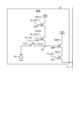
- FIG. 3 is a diagram showing an example of pixel operation. An example of a timing chart when reading out pixel signals is shown.
- Power supply voltage FCVDD is controlled to either 2.4V or 3.3V. Although the power supply voltage FCVDD may be constant, the lower the power supply voltage FCVDD, the higher the possibility of suppressing dark current, so in this example, the power supply voltage FCVDD is controlled to 3.3V only after the LOFIC period, which will be described later.
- Each gate electrode (gate electrode SELG, etc.) is controlled to either a low voltage that turns off the corresponding transistor or a high voltage that turns on the transistor.
- the period from time t1 to time t3 is a period for reading out the pixel signal (reset voltage signal) when the floating diffusion FD is reset. This period is also referred to as a P phase (Precharge phase) period.
- Gate electrode SELG is maintained at high voltage.
- the gate electrode RSTG and the gate electrode FDGG become high voltage, and the floating diffusion FD is reset.
- the period from time t1 to time t2 is a period in which the conversion efficiency is low (conversion efficiency L), and the gate electrode FDGG is at a high voltage, that is, the transistor FDG is turned on.
- a pixel signal in a state where the capacitance of the floating diffusion FD is expanded is sent to the column signal processing unit 6 via the signal line VL.
- the period from time t2 to time t3 is a period in which the conversion efficiency is high (conversion efficiency H), the gate electrode FDGG becomes a low voltage, and the transistor FDG is turned off. Pixel signals in a state where the capacitance of the floating diffusion FD is not expanded are sent to the column signal processing unit 6 via the signal line VL.
- the period from time t3 to time t5 is a period during which pixel signals corresponding to the charges accumulated in the photoelectric conversion element PD are read out. This period is also referred to as a D phase (Data phase) period.
- the period from time t3 to time t4 is a period of high conversion efficiency (conversion efficiency H), and the gate electrode TGLG becomes a high voltage while the gate electrode FDGG is maintained at a low voltage.
- conversion efficiency H conversion efficiency
- the charges accumulated in the photoelectric conversion element PD are transferred to the floating diffusion FD, and the pixel signal is sent to the column signal processing unit 6 via the signal line VL.
- the period from time t4 to time t5 is a period in which the conversion efficiency is low (conversion efficiency L), and the gate electrode TGLG becomes a high voltage while the gate electrode FDGG is maintained at a high voltage.
- the charges accumulated in the photoelectric conversion element PD are transferred to the floating diffusion FD, and the pixel signal is sent to the column signal processing unit 6 via the signal line VL.
- Time t5 to time t7 is a period in which pixel signals are read out using capacitor FC as well. This period is also referred to as a LOFIC (Lateral Overflow Integration Cpacitor) period. While the gate electrode FDGG is maintained at a high voltage, the gate electrode FCGG also becomes a high voltage. Not only transistor FDG but also transistor FCG is turned on. With the capacitor FC connected to the floating diffusion FD, the pixel signal is sent to the column signal processing unit 6 via the signal line VL. Time t5 to time t6 is a D-phase period, and time t6 to time t7 is a P-phase period.
- LOFIC Lateral Overflow Integration Cpacitor
- the gate electrode RSTG becomes a high voltage, and the floating diffusion FD is reset.
- the above-mentioned DDS processing of the column signal processing section 6 is performed on the pixel signals in the LOFIC period.
- a short period after time t7 is provided as a DOL (Digital Overlap) period. Only during that period, the voltage of the gate electrode SELG is maintained at a high voltage, and the pixel signal is taken out via the signal line VL. It is possible to cope with cases where the amount of received light is extremely large.
- DOL Digital Overlap
- the plurality of pixels 2 are operated by controlling the voltages of the gate electrodes of various transistors.
- layout efficiency can be improved by sharing some gate electrodes.
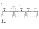
- FIGS. 4 to 6 are diagrams showing a first configuration example of the photodetecting element. Three pixels 2 arranged side by side in the X-axis direction are illustrated.
- FIG. 4 schematically shows a planar layout of each electrode.
- FIG. 5 schematically shows a cross section taken along line VV in FIG. 4.
- FIG. 6 schematically shows a cross section taken along line VI-VI in FIG. Note that in the following description, planar view means viewing the photodetector element 3, that is, the plurality of pixels 2, in a plan view (viewing in the Z-axis direction).
- the photodetector element 3 includes a separation section 4.
- the separation unit 4 separates adjacent pixels 2 from each other.
- the separation by the separation section 4 includes at least one of electrical separation and optical separation.
- the separation section 4 is provided so as to surround each pixel 2 when viewed in plan (when viewed in the Z-axis direction).
- the separation section 4 extends between adjacent pixels 2 in a direction intersecting the XY plane direction, in this example, in the Z-axis direction.
- the separation section 4 can also be said to be a wall section that partitions the adjacent pixels 2.
- Each element of one pixel 2 such as the photoelectric conversion element PD described above, floating diffusion FD, various transistors, capacitor FC, etc., is formed in one region partitioned by the separation section 4.
- the separation part 4 is made of a single layer or a multilayer film of an insulator such as silicon oxide (SiO 2 ), tantalum oxide (Ta 2 O 5 ), hafnium oxide (HfO 2 ), or aluminum oxide (Al 2 O 3 ). may be formed.
- the separation section 4 may be formed of a stacked body of a single layer or multilayer film of an insulator such as tantalum oxide, hafnium oxide, or aluminum oxide, and a silicon oxide film.
- the separation section 4 may have a void therein.
- the separation part 4 may be formed of a metal with high light-shielding properties, such as tantalum (Ta), aluminum (Al), silver (Ag), gold (Au), and copper (Cu). Polycrystalline silicon may be used as the material for the separation part 4.
- the gate electrodes of specific transistors among the plurality of transistors in each of adjacent pixels 2 are arranged on opposite sides of each other with the separation part 4 in between, and the separation part 4 connected to each other beyond.
- the gate electrode FDGG of the transistor FDG, the gate electrode RSTG of the transistor RST, and the gate electrode SELG of the transistor SEL are the gate electrodes of a specific transistor.
- the gates of such specific transistors are connected, for example, by metal wiring extending in the X-axis direction (horizontal direction), so that they can be connected to each other beyond the isolation section 4.
- the gate electrodes of transistors other than the specific transistors are arranged in regions other than the regions between the gate electrodes of the specific transistors of adjacent pixels 2.
- the gate electrode TGLG of the transistor TGL, the gate electrode FCGG of the transistor FCG, the gate electrode OFGG of the transistor OFG, and the gate electrode AMPG of the transistor AMP are This is the gate electrode.
- These gate electrodes TGLG, gate electrode FCGG, gate electrode OFGG, and gate electrode AMPG are located in areas other than the areas between the gate electrodes FDGG of adjacent pixels 2, areas other than the areas between the gate electrodes RSTG, and the gate electrode SELG. It is placed in an area other than the area between them.
- the gate electrodes of each transistor of each adjacent pixel 2 are arranged symmetrically with respect to each other with the separation part 4 in between.
- This arrangement can also be called a mirror arrangement in the X-axis direction (mirror arrangement across the Y-axis). This makes layout design easier. Not only the gate electrode, but also the transistor itself and even other circuit elements may be arranged symmetrically. Note that other patterns not shown may also be provided, such as a ground pattern.
- FIG. 5 schematically shows a cross section of a portion including the gate electrode FDGG and the gate electrode SELG beyond the separation part 4. Illustrations of elements other than the separation section 4 and the gate electrode are omitted. The same applies to other cross-sectional views.
- the gate electrode FDGG includes a first portion P1, a second portion P2, and a third portion P3.
- the first portion P1 of the gate electrode FDGG is a portion located at one of the pixels 2 adjacent in the X-axis direction (in this example, the pixel 2 on the negative side of the X-axis).
- the second portion P2 is a portion located at the other pixel (in this example, pixel 2 on the positive side of the X-axis).
- the third portion P3 is located on the separating portion 4 and is connected between the first portion P1 and the second portion P2.
- Each part of the gate electrode SELG is also referred to as a first part P1, a second part P2, and a third part P3. These are similar to the corresponding portions of the gate electrode FDGG described above.
- FIG. 6 schematically shows a cross section of a portion including the gate electrode RSTG.
- Each portion of the gate electrode RST is also illustrated as a first portion P1, a second portion P2, and a third portion P3. These are also similar to the corresponding portions of the gate electrode FDGG described above.
- the gate electrode of a specific transistor shared between adjacent pixels 2 does not need to be placed apart from the photodetection element 3.
- the layout efficiency can be improved accordingly. For example, by increasing the area of the gate electrode, operation can be stabilized and transfer performance can be improved. It is also possible to suppress signal saturation.
- the electronic device 100 including the photodetector element 3 has advantages such as smaller size and higher performance.
- FIGS. 7 and 8 are diagrams showing a second configuration example of the photodetecting element. Several pixels 2 arranged in a Bayer array are illustrated. In this example, it is assumed that the pixel signals of pixels 2 corresponding to the same color (RED, GREEN, etc.) are read out together in one row at a time.
- FIG. 7 schematically shows a planar layout of each electrode.
- FIG. 8 schematically shows a cross section taken along line VIII-VIII in FIG.
- the transistor OFG of the transistor OFG is also the gate electrode of a specific transistor.
- the gate electrodes OFGG of the transistors OFG of the pixels 2 adjacent to each other in the Y-axis direction are arranged on opposite sides of the separation section 4 and connected to each other across the separation section 4.
- the gate electrode TGLG of the transistor TGL, the gate electrode FCGG of the transistor FCG, and the gate electrode AMPG of the transistor AMP are gate electrodes of transistors other than the specific transistor.
- These gate electrodes TGLG, gate electrode FCGG, and gate electrode AMPG are located in areas other than the areas between the gate electrodes FDGG of adjacent pixels 2, areas other than the areas between the gate electrodes RSTG, and areas other than the area between the gate electrodes SELG.
- the gate electrodes of the respective transistors of the pixels 2 adjacent to each other in the Y-axis direction may be arranged symmetrically with respect to each other with the separation section 4 in between (mirror arrangement in the Y-axis direction (within the X-axis)).
- FIG. 8 schematically shows a cross section of a portion including the gate electrode OFGG beyond the separation part 4.
- Each portion of the gate electrode OFGG is also illustrated as a first portion P1, a second portion P2, and a third portion P3.
- the first portion P1 of the gate electrode OFGG is a portion located at one of the pixels 2 adjacent in the Y-axis direction (in this example, the pixel 2 on the negative side of the Y-axis).
- the second portion P2 is a portion located at the other pixel (in this example, pixel 2 on the positive side of the Y-axis).
- the third portion P3 is located on the separating portion 4 and is connected between the first portion P1 and the second portion P2.
- control line HL_OFG (FIG. 2) connected to the gate electrode OFGG of each pixel 2 adjacent in the Y-axis direction can also be made common.
- the number of control lines HL_OFG for two pixels can be reduced from two to one.
- the degree of freedom in wiring layout is improved. For example, it is possible to improve the RC time constant and reduce the decrease in yield due to dust. Note that the same may be applied to the case of simultaneous reading of four pixels of the same color.
- FIGS. 9 and 10 are diagrams showing a third configuration example of the photodetecting element.
- the pixel arrangement is the same as in FIGS. 7 and 8 described above. However, here, it is assumed that pixel signals of pixels 2 corresponding to different colors adjacent to each other in the Y-axis direction are read out together. In this case, the gate electrodes RSTG of the pixels 2 adjacent to each other in the Y-axis direction are also shared. This is because simultaneous reading allows reset at the same timing.
- FIG. 9 schematically shows a planar layout of each electrode.
- FIG. 10 schematically shows a cross section taken along the line XX in FIG.
- FIG. 10 schematically shows a cross section of a portion including the gate electrode RSTG that exceeds the separation part 4 in the Y-axis direction.
- Each portion of the gate electrode RSTG is also illustrated as a first portion P1, a second portion P2, and a third portion P3. These are similar to the corresponding portions of the above-described gate electrode OFGG (FIG. 8).
- control line HL_RST (FIG. 2) connected to the gate electrode RSTG of each pixel 2 adjacent in the Y-axis direction can also be made common.
- the number of control lines HL can be reduced and the degree of freedom in wiring can be improved.
- FIGS. 11 and 12 are diagrams showing a fourth configuration example of the photodetecting element.
- FIG. 11 shows an example of the circuit of pixel 2.
- FIG. 12 schematically shows a planar layout of each electrode.
- Transistor FDG is connected between floating diffusion FD and transistor RST, and transistor FCG.
- the power supply voltage (node thereof) connected to the transistor RST is shown as a power supply voltage VDD1.
- Transistor AMP is connected between power supply voltage VDD2 different from power supply voltage VDD1 and signal line VL.
- the power supply voltage VDD1 is controlled to be switchable between a high voltage and a low voltage.
- the transistor AMP can have the function of the transistor SEL described above.
- the power supply voltage VDD1 is switched between a high voltage and a low voltage by a control signal of the transistor SEL. Since the pixel 2 does not include the transistor SEL, the circuit configuration is simplified and advantages such as improved layout efficiency can be obtained.
- the gate electrode SELG is also removed from the planar layout.
- the gate electrode FDGG, gate electrode FCGG, and gate electrode OFGG of the pixels 2 adjacent to each other in the X-axis direction are shared. These gate electrodes are connected, for example, by metal wiring extending in the X-axis direction (horizontal direction), so that they can be connected to each other beyond the separation part 4.
- FIGS. 13 and 14 are diagrams showing a fifth configuration example of the photodetecting element.
- FIG. 13 shows a circuit diagram of pixel 2.
- the illustrated pixel 2 differs from the configurations described above in that it does not include the transistor FCG, capacitor FC, and transistor OFG.
- FIG. 14 schematically shows a planar layout of each electrode.
- the gate electrode FDGG, the gate electrode RSTG, and the gate electrode SELG are the gate electrodes of a specific transistor.
- the gate electrodes FDGG of the pixels 2 adjacent to each other in the X-axis direction are arranged on opposite sides of the separation section 4 and connected to each other across the separation section 4 . The same applies to the gate electrode RSTG and the gate electrode SELG.
- FIGS. 15 and 16 are diagrams showing a sixth configuration example of the photodetecting element.
- FIG. 15 shows a circuit diagram of pixel 2.
- the illustrated pixel 2 differs from the configuration of FIG. 13 described above in that it does not include the transistor FDG.
- FIG. 16 schematically shows a planar layout of each electrode.
- Gate electrode RSTG and gate electrode SELG are gate electrodes of a specific transistor.
- FIGS. 17 and 18 are diagrams showing a seventh configuration example of the photodetecting element.
- FIG. 17 shows a circuit diagram of pixel 2.
- the illustrated pixel 2 further includes a photoelectric conversion element PD2, a transistor TGL2, and a floating diffusion FD2, compared to the configuration of FIG. 2 described above.
- Transistor TGL2 is a second transfer transistor for transferring the charge of photoelectric conversion element PD2 to floating diffusion FD2.
- Transistor FCG is connected between floating diffusion FD2, transistor RST, and transistor FDG.
- the gate electrode of the transistor TGL2 is illustrated as a gate electrode TGLG2.
- the control line HL connected to the gate electrode TGLG2 is shown as a control line HL_TGL2.
- the photoelectric conversion element PD and the photoelectric conversion element PD2 have different light receiving sensitivities.
- the photoelectric conversion element PD2 is smaller than the photoelectric conversion element PD, and more specifically, is designed to have a smaller area than the light receiving area of the photoelectric conversion element PD.
- the pixel 2 can also be said to include a large pixel including the photoelectric conversion element PD and a small pixel including the photoelectric conversion element PD2.
- FIG. 18 schematically shows a planar layout of each electrode.
- a region at the center of pixel 2 is indicated by a broken line.
- the photoelectric conversion element PD2 the gate electrode TGLG2 of the transistor TGL2 connected thereto, the floating diffusion FD2, the gate electrode FCGG of the transistor FCG, etc. are arranged.
- photoelectric conversion element PD the gate electrode TGLG of the transistor TGL connected thereto, the gate electrode FDGG of the transistor FDG, the gate electrode RSTG of the transistor RST, the transistor AMP of the transistor AMP, and the transistor SEL A gate electrode SELG and the like are arranged.
- the gate electrode FDGG, the gate electrode RSTG, and the gate electrode SELG are the gate electrodes of a specific transistor.
- the photodetection element 3 As explained with reference to FIGS. 1 to 6, etc., the photodetecting element 3 has a plurality of pixels 2 arranged in the XY plane direction and a structure that separates adjacent pixels 2 among the plurality of pixels 2. A separation section 4 is provided that extends between adjacent pixels 2 in a direction intersecting the XY plane direction (for example, the Z-axis direction).
- Each of the plurality of pixels 2 includes a photoelectric conversion element PD and a plurality of transistors.
- the gate electrodes of specific transistors among the plurality of transistors in each of the adjacent pixels 2 are arranged on opposite sides with the separation section 4 in between. , are connected to each other across the separation part 4.
- the photodetection element 3 described above it is no longer necessary to arrange the gate electrode of a specific transistor apart from the photodetection element 3, for example.
- the layout efficiency can be improved accordingly.
- the gate electrode of a specific transistor is located between the first portion P1 located in one of the adjacent pixels 2 and the gate electrode of a specific transistor located in one of the adjacent pixels 2. , and a third portion P3 located on the separation section 4 and connected between the first portion P1 and the second portion P2. For example, in this way, the gate electrodes of specific transistors of adjacent pixels 2 can be connected to each other across the separation section 4.
- the gate electrodes of transistors other than the specific transistor among the plurality of transistors are located outside the area between the gate electrodes of the specific transistors of adjacent pixels 2. may be placed in the area of For example, by arranging the gate electrodes of each transistor in this manner, the gate electrodes can be shared.
- the gate electrodes of the plurality of transistors in each of the adjacent pixels 2 are arranged symmetrically with the separation section 4 in between. It's fine. This makes layout design easier.
- adjacent pixels 2 are arranged side by side in the X-axis direction (horizontal direction), which is the direction in which the control lines HL of each of the plurality of transistors extend.
- the gate electrode of a specific transistor may include at least one of the gate electrode FDGG of the transistor FDG, the gate electrode RSTG of the transistor RST, the gate electrode SELG of the transistor SEL, and the gate electrode RSTG of the transistor RST.
- the transistor FDG is a conversion efficiency switching transistor for switching the conversion efficiency of the floating diffusion FD that accumulates charges generated in the photoelectric conversion element PD and converts them into voltage.
- Transistor RST is a reset transistor for discharging the charges accumulated in floating diffusion FD.
- the transistor SEL is a selection transistor for selectively outputting a voltage signal (pixel signal) according to the charge accumulated in the floating diffusion FD.
- gate electrodes of specific transistors of such adjacent pixels 2 can be shared.
- adjacent pixels 2 may include two pixels 2 arranged side by side in the Y-axis direction (vertical direction).
- the gate electrode of a specific transistor may include at least one of the gate electrode RSTG of the transistor RST and the gate electrode OFGG of the transistor OFG.
- the transistor OFG is an overflow transistor for transferring the charge overflowing from the photoelectric conversion element PD to, for example, a capacitor FD having an MIM structure.
- gate electrodes of specific transistors of such adjacent pixels 2 can be shared. In this case, the number of control lines HL_RST connected to the shared gate electrode RSTG can be reduced from two to one. Similarly, the number of control lines HL_OFG connected to the shared gate electrode OFGG can be reduced from two to one. Layout efficiency can be further improved.
- each of the plurality of pixels 2 includes a photoelectric conversion element PD2 (second photoelectric conversion element) smaller than the photoelectric conversion element PD, and when viewed in plan, ( When viewed in the Z-axis direction), the gate electrode of the transistor connected to the photoelectric conversion element PD2 of each of the plurality of pixels 2 (gate electrode TGLG2 of the transistor TGL2, etc.) is the gate electrode of the transistor connected to the photoelectric conversion element PD. (The gate electrode TGLG of the transistor TGL, etc.) may be placed closer to the center of the pixel 2. For example, in this way, it is also possible to improve the layout efficiency in a configuration that supports expansion of the dynamic range by using the photoelectric conversion element PD1 and the photoelectric conversion element PD2 together.
- the electronic device 100 including the photodetector element 3 described with reference to FIG. 1 and the like is also one of the techniques disclosed. By providing the photodetector element 3 with improved layout efficiency, the electronic device 100 can be made smaller and have higher performance.
- the technology according to the present disclosure (this technology) can be applied to various products.
- the technology according to the present disclosure may be realized as a device mounted on any type of moving body such as a car, electric vehicle, hybrid electric vehicle, motorcycle, bicycle, personal mobility, airplane, drone, ship, robot, etc. It's okay.
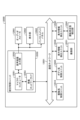
- FIG. 19 is a block diagram showing a schematic configuration example of a vehicle control system, which is an example of a mobile object control system to which the technology according to the present disclosure can be applied.
- the vehicle control system 12000 includes a plurality of electronic control units connected via a communication network 12001.
- the vehicle control system 12000 includes a drive system control unit 12010, a body system control unit 12020, an outside vehicle information detection unit 12030, an inside vehicle information detection unit 12040, and an integrated control unit 12050.
- a microcomputer 12051, an audio/image output section 12052, and an in-vehicle network I/F (Interface) 12053 are illustrated as the functional configuration of the integrated control unit 12050.
- the drive system control unit 12010 controls the operation of devices related to the drive system of the vehicle according to various programs.
- the drive system control unit 12010 includes a drive force generation device such as an internal combustion engine or a drive motor that generates drive force for the vehicle, a drive force transmission mechanism that transmits the drive force to wheels, and a drive force transmission mechanism that controls the steering angle of the vehicle. It functions as a control device for a steering mechanism to adjust and a braking device to generate braking force for the vehicle.
- the body system control unit 12020 controls the operations of various devices installed in the vehicle body according to various programs.
- the body system control unit 12020 functions as a keyless entry system, a smart key system, a power window device, or a control device for various lamps such as a headlamp, a back lamp, a brake lamp, a turn signal, or a fog lamp.
- radio waves transmitted from a portable device that replaces a key or signals from various switches may be input to the body control unit 12020.
- the body system control unit 12020 receives input of these radio waves or signals, and controls the door lock device, power window device, lamp, etc. of the vehicle.
- the external information detection unit 12030 detects information external to the vehicle in which the vehicle control system 12000 is mounted.
- an imaging section 12031 is connected to the outside-vehicle information detection unit 12030.
- the vehicle exterior information detection unit 12030 causes the imaging unit 12031 to capture an image of the exterior of the vehicle, and receives the captured image.
- the external information detection unit 12030 may perform object detection processing such as a person, car, obstacle, sign, or text on the road surface or distance detection processing based on the received image.
- the imaging unit 12031 is an optical sensor that receives light and outputs an electrical signal according to the amount of received light.
- the imaging unit 12031 can output the electrical signal as an image or as distance measurement information.
- the light received by the imaging unit 12031 may be visible light or non-visible light such as infrared rays.
- the in-vehicle information detection unit 12040 detects in-vehicle information.
- a driver condition detection section 12041 that detects the condition of the driver is connected to the in-vehicle information detection unit 12040.
- the driver condition detection unit 12041 includes, for example, a camera that images the driver, and the in-vehicle information detection unit 12040 detects the degree of fatigue or concentration of the driver based on the detection information input from the driver condition detection unit 12041. It may be calculated, or it may be determined whether the driver is falling asleep.
- the microcomputer 12051 calculates control target values for the driving force generation device, steering mechanism, or braking device based on the information inside and outside the vehicle acquired by the vehicle exterior information detection unit 12030 or the vehicle interior information detection unit 12040, Control commands can be output to 12010.
- the microcomputer 12051 realizes ADAS (Advanced Driver Assistance System) functions, including vehicle collision avoidance or shock mitigation, following distance based on vehicle distance, vehicle speed maintenance, vehicle collision warning, vehicle lane departure warning, etc. It is possible to perform cooperative control for the purpose of ADAS (Advanced Driver Assistance System) functions, including vehicle collision avoidance or shock mitigation, following distance based on vehicle distance, vehicle speed maintenance, vehicle collision warning, vehicle lane departure warning, etc. It is possible to perform cooperative control for the purpose of
- ADAS Advanced Driver Assistance System
- the microcomputer 12051 controls the driving force generating device, steering mechanism, braking device, etc. based on information about the surroundings of the vehicle acquired by the vehicle exterior information detection unit 12030 or the vehicle interior information detection unit 12040. It is possible to perform cooperative control for the purpose of autonomous driving, etc., which does not rely on operation.
- the microcomputer 12051 can output a control command to the body system control unit 12020 based on the information outside the vehicle acquired by the outside information detection unit 12030.
- the microcomputer 12051 controls the headlamps according to the position of the preceding vehicle or oncoming vehicle detected by the vehicle exterior information detection unit 12030, and performs cooperative control for the purpose of preventing glare, such as switching from high beam to low beam. It can be carried out.
- the audio and image output unit 12052 transmits an output signal of at least one of audio and images to an output device that can visually or audibly notify information to the occupants of the vehicle or to the outside of the vehicle.
- an audio speaker 12061, a display section 12062, and an instrument panel 12063 are illustrated as output devices.
- the display unit 12062 may include, for example, at least one of an on-board display and a head-up display.
- FIG. 20 is a diagram showing an example of the installation position of the imaging section 12031.
- the imaging unit 12031 includes imaging units 12101, 12102, 12103, 12104, and 12105.
- the imaging units 12101, 12102, 12103, 12104, and 12105 are provided at, for example, the front nose of the vehicle 12100, the side mirrors, the rear bumper, the back door, and the upper part of the windshield inside the vehicle.
- An imaging unit 12101 provided in the front nose and an imaging unit 12105 provided above the windshield inside the vehicle mainly acquire images in front of the vehicle 12100.
- Imaging units 12102 and 12103 provided in the side mirrors mainly capture images of the sides of the vehicle 12100.
- An imaging unit 12104 provided in the rear bumper or back door mainly captures images of the rear of the vehicle 12100.
- the imaging unit 12105 provided above the windshield inside the vehicle is mainly used to detect preceding vehicles, pedestrians, obstacles, traffic lights, traffic signs, lanes, and the like.
- FIG. 20 shows an example of the imaging range of the imaging units 12101 to 12104.
- An imaging range 12111 indicates the imaging range of the imaging unit 12101 provided on the front nose
- imaging ranges 12112 and 12113 indicate imaging ranges of the imaging units 12102 and 12103 provided on the side mirrors, respectively
- an imaging range 12114 shows the imaging range of the imaging unit 12101 provided on the front nose.
- the imaging range of the imaging unit 12104 provided in the rear bumper or back door is shown. For example, by overlapping the image data captured by the imaging units 12101 to 12104, an overhead image of the vehicle 12100 viewed from above can be obtained.
- At least one of the imaging units 12101 to 12104 may have a function of acquiring distance information.
- at least one of the imaging units 12101 to 12104 may be a stereo camera including a plurality of image sensors, or may be an image sensor having pixels for phase difference detection.
- the microcomputer 12051 determines the distance to each three-dimensional object within the imaging ranges 12111 to 12114 and the temporal change in this distance (relative speed with respect to the vehicle 12100) based on the distance information obtained from the imaging units 12101 to 12104. By determining the following, it is possible to extract, in particular, the closest three-dimensional object on the path of vehicle 12100, which is traveling at a predetermined speed (for example, 0 km/h or more) in approximately the same direction as vehicle 12100, as the preceding vehicle. can. Furthermore, the microcomputer 12051 can set an inter-vehicle distance to be secured in advance in front of the preceding vehicle, and perform automatic brake control (including follow-up stop control), automatic acceleration control (including follow-up start control), and the like. In this way, it is possible to perform cooperative control for the purpose of autonomous driving, etc., in which the vehicle travels autonomously without depending on the driver's operation.
- automatic brake control including follow-up stop control
- automatic acceleration control including follow-up start control
- the microcomputer 12051 transfers three-dimensional object data to other three-dimensional objects such as two-wheeled vehicles, regular vehicles, large vehicles, pedestrians, and utility poles based on the distance information obtained from the imaging units 12101 to 12104. It can be classified and extracted and used for automatic obstacle avoidance. For example, the microcomputer 12051 identifies obstacles around the vehicle 12100 into obstacles that are visible to the driver of the vehicle 12100 and obstacles that are difficult to see. Then, the microcomputer 12051 determines a collision risk indicating the degree of risk of collision with each obstacle, and when the collision risk exceeds a set value and there is a possibility of a collision, the microcomputer 12051 transmits information via the audio speaker 12061 and the display unit 12062. By outputting a warning to the driver via the vehicle control unit 12010 and performing forced deceleration and avoidance steering via the drive system control unit 12010, driving support for collision avoidance can be provided.
- the microcomputer 12051 determines a collision risk indicating the degree of risk of collision with each obstacle, and when the collision risk exceed
- At least one of the imaging units 12101 to 12104 may be an infrared camera that detects infrared rays.
- the microcomputer 12051 can recognize a pedestrian by determining whether the pedestrian is present in the images captured by the imaging units 12101 to 12104.
- pedestrian recognition involves, for example, a procedure for extracting feature points in images captured by the imaging units 12101 to 12104 as infrared cameras, and a pattern matching process is performed on a series of feature points indicating the outline of an object to determine whether it is a pedestrian or not.
- the audio image output unit 12052 creates a rectangular outline for emphasis on the recognized pedestrian.
- the display unit 12062 is controlled to display the .
- the audio image output unit 12052 may control the display unit 12062 to display an icon or the like indicating a pedestrian at a desired position.
- the technology according to the present disclosure can be applied to, for example, the imaging unit 12031 among the configurations described above.
- the imaging unit 12031 can be made smaller, have higher performance, and the like.
- the present technology can also have the following configuration.
- the gate electrode of the specific transistor is a first portion located at one of the adjacent pixels; a second portion located at the other pixel of the adjacent pixels; a third part located on the separation part and connected between the first part and the second part; including, The photodetector element according to (1).
- the gate electrodes of the transistors other than the specific transistor among the plurality of transistors are arranged in a region other than the region between the gate electrodes of the specific transistors of each of the adjacent pixels.
- gate electrodes of the plurality of transistors of each of the adjacent pixels are arranged symmetrically with the separation portion interposed therebetween; The photodetecting element according to any one of (1) to (3).
- the adjacent pixels include two pixels arranged side by side in a horizontal direction, which is a direction in which a control line of each of the plurality of transistors extends.
- the photodetector element according to any one of (1) to (4).
- the gate electrode of the specific transistor is a gate electrode of a conversion efficiency switching transistor for switching the conversion efficiency of a floating diffusion that accumulates charge generated in the photoelectric conversion element and converts it into voltage; a gate electrode of a reset transistor for discharging charges accumulated in a floating diffusion that accumulates charges generated in the photoelectric conversion element and changes into voltage; as well as, a gate electrode of a selection transistor for selectively outputting a voltage signal according to the charges accumulated in a floating diffusion that accumulates charges generated in the photoelectric conversion element and changes into voltage; including at least one of The photodetecting element according to (5).
- the adjacent pixels include two pixels arranged side by side in a vertical direction perpendicular to a horizontal direction in which control lines of each of the plurality of transistors extend.
- the photodetecting element according to any one of (1) to (6).
- the gate electrode of the specific transistor is a gate electrode of a reset transistor for discharging charges accumulated in a floating diffusion that accumulates charges generated in the photoelectric conversion element and changes into voltage; as well as, a gate electrode of an overflow transistor for transferring charge overflowing from the photoelectric conversion element to a capacitor; including at least one of The photodetector element according to (7).
- the capacitor has an MIM (Metal-Insulator-Metal) structure, The photodetecting element according to (8).
- Each of the plurality of pixels includes a second photoelectric conversion element smaller than the photoelectric conversion element, When viewed in plan, the gate electrode of the transistor connected to the second photoelectric conversion element of each of the plurality of pixels is closer to the center of the pixel than the gate electrode of the transistor connected to the photoelectric conversion element. be placed, The photodetecting element according to any one of (1) to (9).
- the photodetecting element is Multiple pixels arranged in a plane direction, a separating section extending between the adjacent pixels in a direction intersecting the plane direction so as to separate adjacent pixels among the plurality of pixels; including;
- Each of the plurality of pixels is A photoelectric conversion element, multiple transistors, including; When viewed in plan, the gate electrodes of specific transistors of the plurality of transistors of each of the adjacent pixels are arranged on opposite sides of the separation section, and are arranged on opposite sides of the separation section, and are arranged on opposite sides of each other across the separation section. connected, Electronics.
Landscapes
- Engineering & Computer Science (AREA)
- Multimedia (AREA)
- Signal Processing (AREA)
- Physics & Mathematics (AREA)
- Power Engineering (AREA)
- Electromagnetism (AREA)
- Condensed Matter Physics & Semiconductors (AREA)
- General Physics & Mathematics (AREA)
- Computer Hardware Design (AREA)
- Microelectronics & Electronic Packaging (AREA)
- Solid State Image Pick-Up Elements (AREA)
- Transforming Light Signals Into Electric Signals (AREA)
Abstract
La présente invention concerne un élément de détection de lumière qui comprend : une pluralité de pixels qui sont disposés dans la direction plane ; et une partie de séparation qui s'étend entre des pixels adjacents dans une direction croisant la direction plane de sorte que des pixels adjacents parmi une pluralité de pixels soient séparés les uns des autres, la pluralité de pixels comprenant chacun un élément de conversion photoélectrique et une pluralité de transistors, et, dans une vue en plan, des électrodes de grille de transistors spécifiques respectifs parmi la pluralité de transistors de chacun des pixels adjacents étant disposées en regard les unes des autres avec la partie de séparation entre elles, et étant reliées les unes aux autres à travers la partie de séparation.
Applications Claiming Priority (2)
| Application Number | Priority Date | Filing Date | Title |
|---|---|---|---|
| JP2022-135713 | 2022-08-29 | ||
| JP2022135713A JP2024032194A (ja) | 2022-08-29 | 2022-08-29 | 光検出素子及び電子機器 |
Publications (1)
| Publication Number | Publication Date |
|---|---|
| WO2024048301A1 true WO2024048301A1 (fr) | 2024-03-07 |
Family
ID=90099412
Family Applications (1)
| Application Number | Title | Priority Date | Filing Date |
|---|---|---|---|
| PCT/JP2023/029717 WO2024048301A1 (fr) | 2022-08-29 | 2023-08-17 | Élément de détection de lumière et dispositif électronique |
Country Status (2)
| Country | Link |
|---|---|
| JP (1) | JP2024032194A (fr) |
| WO (1) | WO2024048301A1 (fr) |
Citations (3)
| Publication number | Priority date | Publication date | Assignee | Title |
|---|---|---|---|---|
| WO2017169216A1 (fr) * | 2016-03-31 | 2017-10-05 | ソニー株式会社 | Élément d'imagerie à semi-conducteurs, procédé de commande d'élément d'imagerie à semi-conducteurs et dispositif électronique |
| JP2019080305A (ja) * | 2017-10-20 | 2019-05-23 | ソニーセミコンダクタソリューションズ株式会社 | 固体撮像素子、固体撮像素子の駆動方法および電子機器 |
| JP2020013817A (ja) * | 2018-07-13 | 2020-01-23 | ソニーセミコンダクタソリューションズ株式会社 | 固体撮像素子および電子機器 |
-
2022
- 2022-08-29 JP JP2022135713A patent/JP2024032194A/ja active Pending
-
2023
- 2023-08-17 WO PCT/JP2023/029717 patent/WO2024048301A1/fr unknown
Patent Citations (3)
| Publication number | Priority date | Publication date | Assignee | Title |
|---|---|---|---|---|
| WO2017169216A1 (fr) * | 2016-03-31 | 2017-10-05 | ソニー株式会社 | Élément d'imagerie à semi-conducteurs, procédé de commande d'élément d'imagerie à semi-conducteurs et dispositif électronique |
| JP2019080305A (ja) * | 2017-10-20 | 2019-05-23 | ソニーセミコンダクタソリューションズ株式会社 | 固体撮像素子、固体撮像素子の駆動方法および電子機器 |
| JP2020013817A (ja) * | 2018-07-13 | 2020-01-23 | ソニーセミコンダクタソリューションズ株式会社 | 固体撮像素子および電子機器 |
Also Published As
| Publication number | Publication date |
|---|---|
| JP2024032194A (ja) | 2024-03-12 |
Similar Documents
| Publication | Publication Date | Title |
|---|---|---|
| WO2021054183A1 (fr) | Dispositif d'imagerie à semi-conducteurs et dispositif d'imagerie à fonctions combinées de capteur de vision dynamique et d'imagerie | |
| JP2020145427A (ja) | 固体撮像装置、および、撮像システム | |
| KR20230028422A (ko) | 고체 촬상 장치 | |
| TW202123680A (zh) | 固態成像裝置及具有共享電路元件之成像裝置 | |
| US20220013557A1 (en) | Solid-state imaging device and electronic apparatus | |
| WO2020045142A1 (fr) | Dispositif d'imagerie et instrument électronique | |
| US20220392936A1 (en) | Solid-state imaging device and method of producing the same | |
| US20230013149A1 (en) | Solid-state image pickup device and electronic apparatus | |
| WO2024048301A1 (fr) | Élément de détection de lumière et dispositif électronique | |
| WO2021261070A1 (fr) | Dispositif d'imagerie à semi-conducteurs, et dispositif d'imagerie | |
| US20220103775A1 (en) | Imaging device | |
| WO2024084865A1 (fr) | Dispositif à semi-conducteurs | |
| US20240064433A1 (en) | Imaging element and imaging device | |
| WO2019031089A1 (fr) | Dispositif d'imagerie | |
| WO2023181657A1 (fr) | Dispositif de détection de lumière et appareil électronique | |
| WO2023026576A1 (fr) | Dispositif d'imagerie et appareil électronique | |
| WO2023188868A1 (fr) | Capteur linéaire | |
| WO2023013178A1 (fr) | Dispositif d'imagerie à semi-conducteurs et appareil électronique | |
| TWI835928B (zh) | 固態攝像裝置及電子機器 | |
| WO2023127512A1 (fr) | Dispositif d'imagerie et appareil électronique | |
| US11438534B2 (en) | Solid-state imaging device and electronic apparatus | |
| WO2023100547A1 (fr) | Dispositif d'imagerie et appareil électronique | |
| WO2022080124A1 (fr) | Dispositif d'imagerie et son procédé de fabrication | |
| WO2024042896A1 (fr) | Élément de détection optique et dispositif électronique | |
| CN114424523A (zh) | 固态摄像装置 |
Legal Events
| Date | Code | Title | Description |
|---|---|---|---|
| 121 | Ep: the epo has been informed by wipo that ep was designated in this application |
Ref document number: 23860065 Country of ref document: EP Kind code of ref document: A1 |