WO2024048301A1 - Light detection element and electronic device - Google Patents
Light detection element and electronic device Download PDFInfo
- Publication number
- WO2024048301A1 WO2024048301A1 PCT/JP2023/029717 JP2023029717W WO2024048301A1 WO 2024048301 A1 WO2024048301 A1 WO 2024048301A1 JP 2023029717 W JP2023029717 W JP 2023029717W WO 2024048301 A1 WO2024048301 A1 WO 2024048301A1
- Authority
- WO
- WIPO (PCT)
- Prior art keywords
- transistor
- gate electrode
- pixels
- transistors
- photoelectric conversion
- Prior art date
Links
- 238000001514 detection method Methods 0.000 title abstract description 26
- 238000006243 chemical reaction Methods 0.000 claims abstract description 87
- 238000000926 separation method Methods 0.000 claims abstract description 58
- 238000009792 diffusion process Methods 0.000 claims description 44
- 238000007667 floating Methods 0.000 claims description 44
- 239000003990 capacitor Substances 0.000 claims description 22
- 238000007599 discharging Methods 0.000 claims description 6
- 229910052751 metal Inorganic materials 0.000 claims description 6
- 239000002184 metal Substances 0.000 claims description 6
- 238000003384 imaging method Methods 0.000 description 43
- 238000012545 processing Methods 0.000 description 36
- 238000010586 diagram Methods 0.000 description 20
- 230000000875 corresponding effect Effects 0.000 description 13
- 238000005516 engineering process Methods 0.000 description 13
- 238000000034 method Methods 0.000 description 13
- 238000002955 isolation Methods 0.000 description 7
- 102100036285 25-hydroxyvitamin D-1 alpha hydroxylase, mitochondrial Human genes 0.000 description 6
- 101000875403 Homo sapiens 25-hydroxyvitamin D-1 alpha hydroxylase, mitochondrial Proteins 0.000 description 6
- 101100099196 Saccharomyces cerevisiae (strain ATCC 204508 / S288c) TGL2 gene Proteins 0.000 description 6
- 238000012546 transfer Methods 0.000 description 6
- 230000007246 mechanism Effects 0.000 description 5
- 230000008569 process Effects 0.000 description 5
- 230000007423 decrease Effects 0.000 description 4
- 230000008859 change Effects 0.000 description 3
- 230000000694 effects Effects 0.000 description 3
- 239000012212 insulator Substances 0.000 description 3
- 230000002093 peripheral effect Effects 0.000 description 3
- 239000000758 substrate Substances 0.000 description 3
- VYPSYNLAJGMNEJ-UHFFFAOYSA-N Silicium dioxide Chemical compound O=[Si]=O VYPSYNLAJGMNEJ-UHFFFAOYSA-N 0.000 description 2
- 230000005540 biological transmission Effects 0.000 description 2
- 230000001276 controlling effect Effects 0.000 description 2
- 239000010949 copper Substances 0.000 description 2
- 238000013461 design Methods 0.000 description 2
- 239000010931 gold Substances 0.000 description 2
- 238000009434 installation Methods 0.000 description 2
- 230000010354 integration Effects 0.000 description 2
- 230000003287 optical effect Effects 0.000 description 2
- TWNQGVIAIRXVLR-UHFFFAOYSA-N oxo(oxoalumanyloxy)alumane Chemical compound O=[Al]O[Al]=O TWNQGVIAIRXVLR-UHFFFAOYSA-N 0.000 description 2
- BPUBBGLMJRNUCC-UHFFFAOYSA-N oxygen(2-);tantalum(5+) Chemical compound [O-2].[O-2].[O-2].[O-2].[O-2].[Ta+5].[Ta+5] BPUBBGLMJRNUCC-UHFFFAOYSA-N 0.000 description 2
- 238000005070 sampling Methods 0.000 description 2
- 239000004065 semiconductor Substances 0.000 description 2
- 230000035945 sensitivity Effects 0.000 description 2
- 229910052814 silicon oxide Inorganic materials 0.000 description 2
- 239000002356 single layer Substances 0.000 description 2
- 229910018072 Al 2 O 3 Inorganic materials 0.000 description 1
- RYGMFSIKBFXOCR-UHFFFAOYSA-N Copper Chemical compound [Cu] RYGMFSIKBFXOCR-UHFFFAOYSA-N 0.000 description 1
- 229910004298 SiO 2 Inorganic materials 0.000 description 1
- BQCADISMDOOEFD-UHFFFAOYSA-N Silver Chemical compound [Ag] BQCADISMDOOEFD-UHFFFAOYSA-N 0.000 description 1
- 230000001133 acceleration Effects 0.000 description 1
- 229910052782 aluminium Inorganic materials 0.000 description 1
- XAGFODPZIPBFFR-UHFFFAOYSA-N aluminium Chemical compound [Al] XAGFODPZIPBFFR-UHFFFAOYSA-N 0.000 description 1
- 230000003321 amplification Effects 0.000 description 1
- 239000003086 colorant Substances 0.000 description 1
- 238000002485 combustion reaction Methods 0.000 description 1
- 238000004891 communication Methods 0.000 description 1
- 229910052802 copper Inorganic materials 0.000 description 1
- 230000002596 correlated effect Effects 0.000 description 1
- 239000000428 dust Substances 0.000 description 1
- 230000004313 glare Effects 0.000 description 1
- PCHJSUWPFVWCPO-UHFFFAOYSA-N gold Chemical compound [Au] PCHJSUWPFVWCPO-UHFFFAOYSA-N 0.000 description 1
- 229910052737 gold Inorganic materials 0.000 description 1
- 229910000449 hafnium oxide Inorganic materials 0.000 description 1
- WIHZLLGSGQNAGK-UHFFFAOYSA-N hafnium(4+);oxygen(2-) Chemical compound [O-2].[O-2].[Hf+4] WIHZLLGSGQNAGK-UHFFFAOYSA-N 0.000 description 1
- CJNBYAVZURUTKZ-UHFFFAOYSA-N hafnium(iv) oxide Chemical compound O=[Hf]=O CJNBYAVZURUTKZ-UHFFFAOYSA-N 0.000 description 1
- 238000012423 maintenance Methods 0.000 description 1
- 239000000463 material Substances 0.000 description 1
- 238000005259 measurement Methods 0.000 description 1
- 230000000116 mitigating effect Effects 0.000 description 1
- 238000012986 modification Methods 0.000 description 1
- 230000004048 modification Effects 0.000 description 1
- 238000003199 nucleic acid amplification method Methods 0.000 description 1
- 230000001151 other effect Effects 0.000 description 1
- 238000005192 partition Methods 0.000 description 1
- 229910021420 polycrystalline silicon Inorganic materials 0.000 description 1
- 229920006395 saturated elastomer Polymers 0.000 description 1
- 230000035939 shock Effects 0.000 description 1
- 229910052710 silicon Inorganic materials 0.000 description 1
- 239000010703 silicon Substances 0.000 description 1
- 229910052709 silver Inorganic materials 0.000 description 1
- 239000004332 silver Substances 0.000 description 1
- 229910052715 tantalum Inorganic materials 0.000 description 1
- GUVRBAGPIYLISA-UHFFFAOYSA-N tantalum atom Chemical compound [Ta] GUVRBAGPIYLISA-UHFFFAOYSA-N 0.000 description 1
- 229910001936 tantalum oxide Inorganic materials 0.000 description 1
- 230000002123 temporal effect Effects 0.000 description 1
- 239000011800 void material Substances 0.000 description 1
Images


Classifications
-
- H—ELECTRICITY
- H01—ELECTRIC ELEMENTS
- H01L—SEMICONDUCTOR DEVICES NOT COVERED BY CLASS H10
- H01L27/00—Devices consisting of a plurality of semiconductor or other solid-state components formed in or on a common substrate
- H01L27/14—Devices consisting of a plurality of semiconductor or other solid-state components formed in or on a common substrate including semiconductor components sensitive to infrared radiation, light, electromagnetic radiation of shorter wavelength or corpuscular radiation and specially adapted either for the conversion of the energy of such radiation into electrical energy or for the control of electrical energy by such radiation
- H01L27/144—Devices controlled by radiation
- H01L27/146—Imager structures
-
- H—ELECTRICITY
- H04—ELECTRIC COMMUNICATION TECHNIQUE
- H04N—PICTORIAL COMMUNICATION, e.g. TELEVISION
- H04N25/00—Circuitry of solid-state image sensors [SSIS]; Control thereof
- H04N25/70—SSIS architectures; Circuits associated therewith
-
- H—ELECTRICITY
- H04—ELECTRIC COMMUNICATION TECHNIQUE
- H04N—PICTORIAL COMMUNICATION, e.g. TELEVISION
- H04N25/00—Circuitry of solid-state image sensors [SSIS]; Control thereof
- H04N25/70—SSIS architectures; Circuits associated therewith
- H04N25/76—Addressed sensors, e.g. MOS or CMOS sensors
- H04N25/77—Pixel circuitry, e.g. memories, A/D converters, pixel amplifiers, shared circuits or shared components
- H04N25/771—Pixel circuitry, e.g. memories, A/D converters, pixel amplifiers, shared circuits or shared components comprising storage means other than floating diffusion
Definitions
- the present disclosure relates to a photodetector and an electronic device.
- Patent Document 1 discloses an imaging device including a separation section that separates adjacent pixels.
- the presence of the separation portion limits the arrangement of photoelectric conversion elements and transistors within the pixel, reducing layout efficiency.
- One aspect of the present disclosure improves layout efficiency.
- a photodetection element includes a plurality of pixels arranged in a plane direction, and a direction that intersects the plane direction between adjacent pixels so as to separate adjacent pixels among the plurality of pixels.
- a separating section extending in a direction in which each of the plurality of pixels includes a photoelectric conversion element and a plurality of transistors;
- the gate electrodes of the transistors are disposed on opposite sides of the isolation section and are connected to each other across the isolation section.
- An electronic device includes a photodetection element, and the photodetection element includes a plurality of pixels arranged in a planar direction, and a plurality of pixels that are adjacent to each other so as to separate adjacent pixels among the plurality of pixels. a separation portion extending in a direction intersecting the plane direction between matching pixels, each of the plurality of pixels includes a photoelectric conversion element and a plurality of transistors, and when viewed in plan, adjacent pixels The gate electrodes of specific transistors among the plurality of transistors of each pixel are arranged on opposite sides of the separation section, and are connected to each other across the separation section.
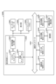
- FIG. 1 is a diagram illustrating an example of a schematic configuration of an electronic device including a photodetection element according to an embodiment.
- FIG. 2 is a circuit diagram showing an example of a schematic configuration of a pixel.
- FIG. 3 is a diagram illustrating an example of pixel operation. It is a figure showing the 1st example of composition of a photodetection element. It is a figure showing the 1st example of composition of a photodetection element. It is a figure showing the 1st example of composition of a photodetection element. It is a figure showing the 2nd example of composition of a photodetection element. It is a figure which shows the 2nd structural example of a photodetection element.
- FIG. 1 is a block diagram showing an example of a schematic configuration of a vehicle control system.
- FIG. 2 is an explanatory diagram showing an example of installation positions of an outside-vehicle information detection section and an imaging section.
- CMOS image sensors (CMOS-type solid-state imaging devices) and the like are known as devices and electronic devices that include photodetecting elements. With the miniaturization technology associated with the CMOS process, it is possible to easily create an active structure with an amplification function for each pixel. Furthermore, a peripheral circuit section such as a signal processing circuit that processes signals output from each pixel of the pixel array section can be integrated on the same chip (substrate) as the pixel array section. Many technologies related to CMOS image sensors have been proposed.
- LOFIC Lateral Overflow Integration Capacitor
- a capacitor is provided within a pixel to directly increase the amount of charge handled.
- one pixel includes photoelectric conversion elements of different sizes with different light-receiving sensitivities.
- a global shutter technique is also known, as disclosed in Patent Document 1, in which exposure is started for all pixels at the same time and exposure is ended for all pixels at the same time.
- a deep insulator such as DTI (Deep Trench Isolation) is sometimes provided as an isolation part.
- DTI Deep Trench Isolation
- the presence of the isolation section surrounding the pixels limits the placement of photoelectric conversion elements and transistors, reducing layout efficiency.
- the gate electrode is placed apart from the isolation part to avoid the risk of short circuits.
- the size of the transistor becomes smaller, which may cause a decrease in the amount of saturated signal, a transfer problem, etc.
- Such problems become more apparent as the number of elements such as transistors increases as pixels become smaller and more sophisticated.
- the elements of adjacent pixels are arranged symmetrically, for example, with the separation section in between.
- transistors located near the separation portion share a gate electrode. This eliminates wasted space and improves layout efficiency.
- FIG. 1 is a diagram illustrating an example of a schematic configuration of an electronic device including a photodetection element according to an embodiment.
- the illustrated electronic device 100 is a CMOS image sensor, and includes a pixel array section 1 and a peripheral section. These elements are formed on a semiconductor substrate, such as silicon.
- a vertical drive section 5 As peripheral parts, in FIG. 1, a vertical drive section 5, a column signal processing section 6, a horizontal drive section 7, a signal processing section 8, and a system control section 9 are illustrated.
- FIG. 1 also shows an XYZ coordinate system for the pixel array section 1.
- the X-axis direction is also referred to as a horizontal direction (lateral direction) or the like.
- the Y-axis direction is also referred to as a vertical direction (longitudinal direction) or the like.
- the Z-axis direction is a direction perpendicular to the XY plane direction, and corresponds to, for example, the thickness direction of the semiconductor substrate.
- the pixel array section 1 includes a plurality of pixels 2.
- the plurality of pixels 2 are two-dimensionally arranged in the X-axis direction and the Y-axis direction.
- Each pixel 2 generates and outputs a voltage signal according to the amount of received light. This signal is also called a pixel signal.
- the photodetecting element 3 includes at least two adjacent pixels among the plurality of pixels 2. As long as there is no contradiction, the light detection element 3 and the plurality of pixels 2 may be read as appropriate.
- the vertical drive section 5 drives the plurality of pixels 2 of the pixel array section 1, for example, all at the same time or for each pixel row. Driving includes selective scanning of the plurality of pixels 2 row by row in order to read out pixel signals. The pixel signal of the selectively scanned pixel 2 is sent to the column signal processing section 6.
- the vertical drive unit 5 is connected to the pixel array unit 1 via a plurality of control lines HL, for example, for each pixel row.
- Each control line HL extends in the row direction and connects each pixel 2 of the corresponding pixel row to the vertical drive unit 5.
- the vertical drive unit 5 includes, for example, a shift register, an address decoder, and the like.
- being connected may be understood to mean being electrically connected.
- Being electrically connected may include being connected with another element interposed therebetween, as long as the functions of the connected elements are not hindered.
- the column signal processing unit 6 processes pixel signals from each pixel 2 in the row selected by the vertical drive unit 5 for each pixel column.
- the column signal processing section 6 includes a plurality of unit circuits corresponding to pixel columns.
- the processing by the column signal processing unit 6 includes noise removal processing, CDS (Correlated Double Sampling) processing, DDS (Double Data Sampling) processing, A/D (Analog/Digital) conversion processing of analog pixel signals, etc. include.
- the pixel signal is digitized and sent to the signal processing section 8.
- the column signal processing section 6 is connected to the pixel array section 1 via a plurality of signal lines VL. Each signal line VL extends in the column direction and connects each pixel 2 of the corresponding pixel column to the column signal processing unit 6.
- the column signal processing section 6 includes, for example, a shift register, an address decoder, and the like.
- the horizontal drive unit 7 sequentially selects the unit circuits of the column signal processing unit 6. Due to this selective scanning by the horizontal driving section 7, pixel signals for each pixel column processed by the column signal processing section 6 are sequentially output to the signal processing section 8.
- the horizontal drive unit 7 includes, for example, a shift register, an address decoder, and the like.
- the signal processing unit 8 processes the pixel signals from the column signal processing unit 6, generates and outputs an image signal based on the pixel signals. Note that the most necessary data for processing may be temporarily stored, for example, in a storage unit (not shown).
- the system control section 9 controls the vertical drive section 5, column signal processing section 6, and horizontal drive section 7.
- the system control unit 9 is configured to include a timing generator and the like to generate various timing signals and supply them to corresponding parts.
- the pixel 2 of the pixel array section 1 will be explained with reference to FIG. 2 as well.
- FIG. 2 is a circuit diagram showing an example of a schematic configuration of a pixel.
- the pixel 2 includes a photoelectric conversion element PD, a floating diffusion FD, a capacitor FC, and a plurality of transistors.
- the plurality of transistors include a transistor TGL, a transistor FDG, a transistor FCG, a transistor OFG, a transistor RST, a transistor AMP, and a transistor SEL.
- the illustrated transistor is a FET, and has a drain and a source that are current terminals, and a gate electrode that is a control terminal. Unless otherwise specified, when a transistor is connected between two elements, it means that one current terminal (drain or source) of the transistor is connected to one element, and the other current terminal of the transistor is connected to the other element. shall mean that the current terminal is connected.
- the gate electrode of the transistor TGL is shown as a gate electrode TGLG.
- the gate electrode of the transistor FDG is illustrated as a gate electrode FDGG.
- the gate electrode of transistor FCG is shown as gate electrode FCGG.
- the gate electrode of the transistor OFG is shown as a gate electrode OFGG.
- the gate electrode of the transistor RST is shown as a gate electrode RSTG.
- the gate electrode of the transistor AMP is illustrated as a gate electrode AMPG.
- the gate electrode of the transistor SEL is shown as a gate electrode SELG. Note that the gate of the transistor AMP is connected to the floating diffusion FD.
- control line HL_TGL the control line HL connected to the gate electrode TGLG of the transistor TGL is referred to as a control line HL_TGL and illustrated.
- the control line HL connected to the gate electrode FDGG of the transistor FDG is illustrated as a control line HL_FDG.
- the control line HL connected to the gate electrode FCGG of the transistor FCG is shown as a control line HL_FCG.
- the control line HL connected to the gate electrode OFGG of the transistor OFG is illustrated as a control line HL_OFG.
- the control line HL connected to the gate electrode RSTG of the transistor RST is shown as a control line HL_RST.
- the control line HL connected to the gate electrode SELG of the transistor SEL is shown as a control line HL_SEL.
- the on/off state (conductive state and non-conductive state) of each transistor is controlled by a control signal from the corresponding control line HL.
- the photoelectric conversion element PD generates and accumulates charges according to the amount of received light.
- An example of the photoelectric conversion element PD is a photodiode or the like.
- the transistor TGL is a transfer transistor for transferring the charge of the photoelectric conversion element PD to the floating diffusion FD.
- Transistor TGL is connected between photoelectric conversion element PD and floating diffusion FD.
- the floating diffusion FD accumulates the charge from the photoelectric conversion element PD transferred via the transfer transistor TGL and converts it into a voltage. A voltage is generated according to the amount of accumulated charge.
- the floating diffusion FD is formed to have a floating diffusion capacitance between at least the transistor TGL, the transistor AMP, and the transistor FDG.
- the transistor FDG is a conversion efficiency switching transistor that switches the conversion efficiency from charge to voltage in the floating diffusion FD.
- Transistor FDG is connected between floating diffusion FD, transistor RST, and transistor FCG.
- the transistor FDG When the transistor FDG is turned on, the region of the floating diffusion FD expands to the region on the opposite side of the floating diffusion FD with FDG in between, and the capacitance of the floating diffusion FD increases accordingly.
- the capacitance of the floating diffusion FD increases, the voltage change corresponding to the change in the amount of stored charge becomes gradual, and the conversion efficiency decreases.
- the transistor FDG is turned off, the capacitance of the floating diffusion FD decreases, and the conversion efficiency increases accordingly.
- the transistor FCG is a capacitive connection transistor for connecting the capacitor FC to the floating diffusion FD.
- Transistor FCG is connected between transistor FDG and transistor RST, and capacitor FC and transistor OFG.
- the transistor OFG is an overflow transistor (overflow gate) for transferring the charge overflowing from the photoelectric conversion element PD to the capacitor FC.
- Transistor OFG is connected between photoelectric conversion element PD, capacitor FC, and transistor FCG.
- the capacitor FC is used to store charges overflowing from the photoelectric conversion element PD.
- Capacitor FC is connected between (a node of) power supply voltage FCVDD and transistor OFG and transistor FCG.
- the capacitor FC has, for example, an MIM (Metal-Insulator-Metal) structure, and the capacitor FC in this case is an MIM capacitor.
- the transistor RST is a reset transistor for discharging the charges accumulated in the floating diffusion FD.
- Transistor RST is connected between (a node of) power supply voltage VDD and transistor FDG and transistor FCG.
- the transistor AMP is an amplifier transistor that outputs a voltage signal according to the voltage of the floating diffusion FD.
- Transistor AMP is connected between power supply voltage VDD and transistor SEL.
- the voltage signal output by the transistor AMP can correspond to a pixel signal.
- the transistor SEL is a selection transistor for selectively outputting the voltage signal output by the transistor AMP to the signal line VL.
- Transistor SEL is connected between transistor AMP and signal line VL.
- FIG. 3 is a diagram showing an example of pixel operation. An example of a timing chart when reading out pixel signals is shown.
- Power supply voltage FCVDD is controlled to either 2.4V or 3.3V. Although the power supply voltage FCVDD may be constant, the lower the power supply voltage FCVDD, the higher the possibility of suppressing dark current, so in this example, the power supply voltage FCVDD is controlled to 3.3V only after the LOFIC period, which will be described later.
- Each gate electrode (gate electrode SELG, etc.) is controlled to either a low voltage that turns off the corresponding transistor or a high voltage that turns on the transistor.
- the period from time t1 to time t3 is a period for reading out the pixel signal (reset voltage signal) when the floating diffusion FD is reset. This period is also referred to as a P phase (Precharge phase) period.
- Gate electrode SELG is maintained at high voltage.
- the gate electrode RSTG and the gate electrode FDGG become high voltage, and the floating diffusion FD is reset.
- the period from time t1 to time t2 is a period in which the conversion efficiency is low (conversion efficiency L), and the gate electrode FDGG is at a high voltage, that is, the transistor FDG is turned on.
- a pixel signal in a state where the capacitance of the floating diffusion FD is expanded is sent to the column signal processing unit 6 via the signal line VL.
- the period from time t2 to time t3 is a period in which the conversion efficiency is high (conversion efficiency H), the gate electrode FDGG becomes a low voltage, and the transistor FDG is turned off. Pixel signals in a state where the capacitance of the floating diffusion FD is not expanded are sent to the column signal processing unit 6 via the signal line VL.
- the period from time t3 to time t5 is a period during which pixel signals corresponding to the charges accumulated in the photoelectric conversion element PD are read out. This period is also referred to as a D phase (Data phase) period.
- the period from time t3 to time t4 is a period of high conversion efficiency (conversion efficiency H), and the gate electrode TGLG becomes a high voltage while the gate electrode FDGG is maintained at a low voltage.
- conversion efficiency H conversion efficiency
- the charges accumulated in the photoelectric conversion element PD are transferred to the floating diffusion FD, and the pixel signal is sent to the column signal processing unit 6 via the signal line VL.
- the period from time t4 to time t5 is a period in which the conversion efficiency is low (conversion efficiency L), and the gate electrode TGLG becomes a high voltage while the gate electrode FDGG is maintained at a high voltage.
- the charges accumulated in the photoelectric conversion element PD are transferred to the floating diffusion FD, and the pixel signal is sent to the column signal processing unit 6 via the signal line VL.
- Time t5 to time t7 is a period in which pixel signals are read out using capacitor FC as well. This period is also referred to as a LOFIC (Lateral Overflow Integration Cpacitor) period. While the gate electrode FDGG is maintained at a high voltage, the gate electrode FCGG also becomes a high voltage. Not only transistor FDG but also transistor FCG is turned on. With the capacitor FC connected to the floating diffusion FD, the pixel signal is sent to the column signal processing unit 6 via the signal line VL. Time t5 to time t6 is a D-phase period, and time t6 to time t7 is a P-phase period.
- LOFIC Lateral Overflow Integration Cpacitor
- the gate electrode RSTG becomes a high voltage, and the floating diffusion FD is reset.
- the above-mentioned DDS processing of the column signal processing section 6 is performed on the pixel signals in the LOFIC period.
- a short period after time t7 is provided as a DOL (Digital Overlap) period. Only during that period, the voltage of the gate electrode SELG is maintained at a high voltage, and the pixel signal is taken out via the signal line VL. It is possible to cope with cases where the amount of received light is extremely large.
- DOL Digital Overlap
- the plurality of pixels 2 are operated by controlling the voltages of the gate electrodes of various transistors.
- layout efficiency can be improved by sharing some gate electrodes.
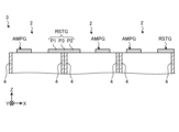
- FIGS. 4 to 6 are diagrams showing a first configuration example of the photodetecting element. Three pixels 2 arranged side by side in the X-axis direction are illustrated.
- FIG. 4 schematically shows a planar layout of each electrode.
- FIG. 5 schematically shows a cross section taken along line VV in FIG. 4.
- FIG. 6 schematically shows a cross section taken along line VI-VI in FIG. Note that in the following description, planar view means viewing the photodetector element 3, that is, the plurality of pixels 2, in a plan view (viewing in the Z-axis direction).
- the photodetector element 3 includes a separation section 4.
- the separation unit 4 separates adjacent pixels 2 from each other.
- the separation by the separation section 4 includes at least one of electrical separation and optical separation.
- the separation section 4 is provided so as to surround each pixel 2 when viewed in plan (when viewed in the Z-axis direction).
- the separation section 4 extends between adjacent pixels 2 in a direction intersecting the XY plane direction, in this example, in the Z-axis direction.
- the separation section 4 can also be said to be a wall section that partitions the adjacent pixels 2.
- Each element of one pixel 2 such as the photoelectric conversion element PD described above, floating diffusion FD, various transistors, capacitor FC, etc., is formed in one region partitioned by the separation section 4.
- the separation part 4 is made of a single layer or a multilayer film of an insulator such as silicon oxide (SiO 2 ), tantalum oxide (Ta 2 O 5 ), hafnium oxide (HfO 2 ), or aluminum oxide (Al 2 O 3 ). may be formed.
- the separation section 4 may be formed of a stacked body of a single layer or multilayer film of an insulator such as tantalum oxide, hafnium oxide, or aluminum oxide, and a silicon oxide film.
- the separation section 4 may have a void therein.
- the separation part 4 may be formed of a metal with high light-shielding properties, such as tantalum (Ta), aluminum (Al), silver (Ag), gold (Au), and copper (Cu). Polycrystalline silicon may be used as the material for the separation part 4.
- the gate electrodes of specific transistors among the plurality of transistors in each of adjacent pixels 2 are arranged on opposite sides of each other with the separation part 4 in between, and the separation part 4 connected to each other beyond.
- the gate electrode FDGG of the transistor FDG, the gate electrode RSTG of the transistor RST, and the gate electrode SELG of the transistor SEL are the gate electrodes of a specific transistor.
- the gates of such specific transistors are connected, for example, by metal wiring extending in the X-axis direction (horizontal direction), so that they can be connected to each other beyond the isolation section 4.
- the gate electrodes of transistors other than the specific transistors are arranged in regions other than the regions between the gate electrodes of the specific transistors of adjacent pixels 2.
- the gate electrode TGLG of the transistor TGL, the gate electrode FCGG of the transistor FCG, the gate electrode OFGG of the transistor OFG, and the gate electrode AMPG of the transistor AMP are This is the gate electrode.
- These gate electrodes TGLG, gate electrode FCGG, gate electrode OFGG, and gate electrode AMPG are located in areas other than the areas between the gate electrodes FDGG of adjacent pixels 2, areas other than the areas between the gate electrodes RSTG, and the gate electrode SELG. It is placed in an area other than the area between them.
- the gate electrodes of each transistor of each adjacent pixel 2 are arranged symmetrically with respect to each other with the separation part 4 in between.
- This arrangement can also be called a mirror arrangement in the X-axis direction (mirror arrangement across the Y-axis). This makes layout design easier. Not only the gate electrode, but also the transistor itself and even other circuit elements may be arranged symmetrically. Note that other patterns not shown may also be provided, such as a ground pattern.
- FIG. 5 schematically shows a cross section of a portion including the gate electrode FDGG and the gate electrode SELG beyond the separation part 4. Illustrations of elements other than the separation section 4 and the gate electrode are omitted. The same applies to other cross-sectional views.
- the gate electrode FDGG includes a first portion P1, a second portion P2, and a third portion P3.
- the first portion P1 of the gate electrode FDGG is a portion located at one of the pixels 2 adjacent in the X-axis direction (in this example, the pixel 2 on the negative side of the X-axis).
- the second portion P2 is a portion located at the other pixel (in this example, pixel 2 on the positive side of the X-axis).
- the third portion P3 is located on the separating portion 4 and is connected between the first portion P1 and the second portion P2.
- Each part of the gate electrode SELG is also referred to as a first part P1, a second part P2, and a third part P3. These are similar to the corresponding portions of the gate electrode FDGG described above.
- FIG. 6 schematically shows a cross section of a portion including the gate electrode RSTG.
- Each portion of the gate electrode RST is also illustrated as a first portion P1, a second portion P2, and a third portion P3. These are also similar to the corresponding portions of the gate electrode FDGG described above.
- the gate electrode of a specific transistor shared between adjacent pixels 2 does not need to be placed apart from the photodetection element 3.
- the layout efficiency can be improved accordingly. For example, by increasing the area of the gate electrode, operation can be stabilized and transfer performance can be improved. It is also possible to suppress signal saturation.
- the electronic device 100 including the photodetector element 3 has advantages such as smaller size and higher performance.
- FIGS. 7 and 8 are diagrams showing a second configuration example of the photodetecting element. Several pixels 2 arranged in a Bayer array are illustrated. In this example, it is assumed that the pixel signals of pixels 2 corresponding to the same color (RED, GREEN, etc.) are read out together in one row at a time.
- FIG. 7 schematically shows a planar layout of each electrode.
- FIG. 8 schematically shows a cross section taken along line VIII-VIII in FIG.
- the transistor OFG of the transistor OFG is also the gate electrode of a specific transistor.
- the gate electrodes OFGG of the transistors OFG of the pixels 2 adjacent to each other in the Y-axis direction are arranged on opposite sides of the separation section 4 and connected to each other across the separation section 4.
- the gate electrode TGLG of the transistor TGL, the gate electrode FCGG of the transistor FCG, and the gate electrode AMPG of the transistor AMP are gate electrodes of transistors other than the specific transistor.
- These gate electrodes TGLG, gate electrode FCGG, and gate electrode AMPG are located in areas other than the areas between the gate electrodes FDGG of adjacent pixels 2, areas other than the areas between the gate electrodes RSTG, and areas other than the area between the gate electrodes SELG.
- the gate electrodes of the respective transistors of the pixels 2 adjacent to each other in the Y-axis direction may be arranged symmetrically with respect to each other with the separation section 4 in between (mirror arrangement in the Y-axis direction (within the X-axis)).
- FIG. 8 schematically shows a cross section of a portion including the gate electrode OFGG beyond the separation part 4.
- Each portion of the gate electrode OFGG is also illustrated as a first portion P1, a second portion P2, and a third portion P3.
- the first portion P1 of the gate electrode OFGG is a portion located at one of the pixels 2 adjacent in the Y-axis direction (in this example, the pixel 2 on the negative side of the Y-axis).
- the second portion P2 is a portion located at the other pixel (in this example, pixel 2 on the positive side of the Y-axis).
- the third portion P3 is located on the separating portion 4 and is connected between the first portion P1 and the second portion P2.
- control line HL_OFG (FIG. 2) connected to the gate electrode OFGG of each pixel 2 adjacent in the Y-axis direction can also be made common.
- the number of control lines HL_OFG for two pixels can be reduced from two to one.
- the degree of freedom in wiring layout is improved. For example, it is possible to improve the RC time constant and reduce the decrease in yield due to dust. Note that the same may be applied to the case of simultaneous reading of four pixels of the same color.
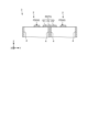
- FIGS. 9 and 10 are diagrams showing a third configuration example of the photodetecting element.
- the pixel arrangement is the same as in FIGS. 7 and 8 described above. However, here, it is assumed that pixel signals of pixels 2 corresponding to different colors adjacent to each other in the Y-axis direction are read out together. In this case, the gate electrodes RSTG of the pixels 2 adjacent to each other in the Y-axis direction are also shared. This is because simultaneous reading allows reset at the same timing.
- FIG. 9 schematically shows a planar layout of each electrode.
- FIG. 10 schematically shows a cross section taken along the line XX in FIG.
- FIG. 10 schematically shows a cross section of a portion including the gate electrode RSTG that exceeds the separation part 4 in the Y-axis direction.
- Each portion of the gate electrode RSTG is also illustrated as a first portion P1, a second portion P2, and a third portion P3. These are similar to the corresponding portions of the above-described gate electrode OFGG (FIG. 8).
- control line HL_RST (FIG. 2) connected to the gate electrode RSTG of each pixel 2 adjacent in the Y-axis direction can also be made common.
- the number of control lines HL can be reduced and the degree of freedom in wiring can be improved.
- FIGS. 11 and 12 are diagrams showing a fourth configuration example of the photodetecting element.
- FIG. 11 shows an example of the circuit of pixel 2.
- FIG. 12 schematically shows a planar layout of each electrode.
- Transistor FDG is connected between floating diffusion FD and transistor RST, and transistor FCG.
- the power supply voltage (node thereof) connected to the transistor RST is shown as a power supply voltage VDD1.
- Transistor AMP is connected between power supply voltage VDD2 different from power supply voltage VDD1 and signal line VL.
- the power supply voltage VDD1 is controlled to be switchable between a high voltage and a low voltage.
- the transistor AMP can have the function of the transistor SEL described above.
- the power supply voltage VDD1 is switched between a high voltage and a low voltage by a control signal of the transistor SEL. Since the pixel 2 does not include the transistor SEL, the circuit configuration is simplified and advantages such as improved layout efficiency can be obtained.
- the gate electrode SELG is also removed from the planar layout.
- the gate electrode FDGG, gate electrode FCGG, and gate electrode OFGG of the pixels 2 adjacent to each other in the X-axis direction are shared. These gate electrodes are connected, for example, by metal wiring extending in the X-axis direction (horizontal direction), so that they can be connected to each other beyond the separation part 4.
- FIGS. 13 and 14 are diagrams showing a fifth configuration example of the photodetecting element.
- FIG. 13 shows a circuit diagram of pixel 2.
- the illustrated pixel 2 differs from the configurations described above in that it does not include the transistor FCG, capacitor FC, and transistor OFG.
- FIG. 14 schematically shows a planar layout of each electrode.
- the gate electrode FDGG, the gate electrode RSTG, and the gate electrode SELG are the gate electrodes of a specific transistor.
- the gate electrodes FDGG of the pixels 2 adjacent to each other in the X-axis direction are arranged on opposite sides of the separation section 4 and connected to each other across the separation section 4 . The same applies to the gate electrode RSTG and the gate electrode SELG.
- FIGS. 15 and 16 are diagrams showing a sixth configuration example of the photodetecting element.
- FIG. 15 shows a circuit diagram of pixel 2.
- the illustrated pixel 2 differs from the configuration of FIG. 13 described above in that it does not include the transistor FDG.
- FIG. 16 schematically shows a planar layout of each electrode.
- Gate electrode RSTG and gate electrode SELG are gate electrodes of a specific transistor.
- FIGS. 17 and 18 are diagrams showing a seventh configuration example of the photodetecting element.
- FIG. 17 shows a circuit diagram of pixel 2.
- the illustrated pixel 2 further includes a photoelectric conversion element PD2, a transistor TGL2, and a floating diffusion FD2, compared to the configuration of FIG. 2 described above.
- Transistor TGL2 is a second transfer transistor for transferring the charge of photoelectric conversion element PD2 to floating diffusion FD2.
- Transistor FCG is connected between floating diffusion FD2, transistor RST, and transistor FDG.
- the gate electrode of the transistor TGL2 is illustrated as a gate electrode TGLG2.
- the control line HL connected to the gate electrode TGLG2 is shown as a control line HL_TGL2.
- the photoelectric conversion element PD and the photoelectric conversion element PD2 have different light receiving sensitivities.
- the photoelectric conversion element PD2 is smaller than the photoelectric conversion element PD, and more specifically, is designed to have a smaller area than the light receiving area of the photoelectric conversion element PD.
- the pixel 2 can also be said to include a large pixel including the photoelectric conversion element PD and a small pixel including the photoelectric conversion element PD2.
- FIG. 18 schematically shows a planar layout of each electrode.
- a region at the center of pixel 2 is indicated by a broken line.
- the photoelectric conversion element PD2 the gate electrode TGLG2 of the transistor TGL2 connected thereto, the floating diffusion FD2, the gate electrode FCGG of the transistor FCG, etc. are arranged.
- photoelectric conversion element PD the gate electrode TGLG of the transistor TGL connected thereto, the gate electrode FDGG of the transistor FDG, the gate electrode RSTG of the transistor RST, the transistor AMP of the transistor AMP, and the transistor SEL A gate electrode SELG and the like are arranged.
- the gate electrode FDGG, the gate electrode RSTG, and the gate electrode SELG are the gate electrodes of a specific transistor.
- the photodetection element 3 As explained with reference to FIGS. 1 to 6, etc., the photodetecting element 3 has a plurality of pixels 2 arranged in the XY plane direction and a structure that separates adjacent pixels 2 among the plurality of pixels 2. A separation section 4 is provided that extends between adjacent pixels 2 in a direction intersecting the XY plane direction (for example, the Z-axis direction).
- Each of the plurality of pixels 2 includes a photoelectric conversion element PD and a plurality of transistors.
- the gate electrodes of specific transistors among the plurality of transistors in each of the adjacent pixels 2 are arranged on opposite sides with the separation section 4 in between. , are connected to each other across the separation part 4.
- the photodetection element 3 described above it is no longer necessary to arrange the gate electrode of a specific transistor apart from the photodetection element 3, for example.
- the layout efficiency can be improved accordingly.
- the gate electrode of a specific transistor is located between the first portion P1 located in one of the adjacent pixels 2 and the gate electrode of a specific transistor located in one of the adjacent pixels 2. , and a third portion P3 located on the separation section 4 and connected between the first portion P1 and the second portion P2. For example, in this way, the gate electrodes of specific transistors of adjacent pixels 2 can be connected to each other across the separation section 4.
- the gate electrodes of transistors other than the specific transistor among the plurality of transistors are located outside the area between the gate electrodes of the specific transistors of adjacent pixels 2. may be placed in the area of For example, by arranging the gate electrodes of each transistor in this manner, the gate electrodes can be shared.
- the gate electrodes of the plurality of transistors in each of the adjacent pixels 2 are arranged symmetrically with the separation section 4 in between. It's fine. This makes layout design easier.
- adjacent pixels 2 are arranged side by side in the X-axis direction (horizontal direction), which is the direction in which the control lines HL of each of the plurality of transistors extend.
- the gate electrode of a specific transistor may include at least one of the gate electrode FDGG of the transistor FDG, the gate electrode RSTG of the transistor RST, the gate electrode SELG of the transistor SEL, and the gate electrode RSTG of the transistor RST.
- the transistor FDG is a conversion efficiency switching transistor for switching the conversion efficiency of the floating diffusion FD that accumulates charges generated in the photoelectric conversion element PD and converts them into voltage.
- Transistor RST is a reset transistor for discharging the charges accumulated in floating diffusion FD.
- the transistor SEL is a selection transistor for selectively outputting a voltage signal (pixel signal) according to the charge accumulated in the floating diffusion FD.
- gate electrodes of specific transistors of such adjacent pixels 2 can be shared.
- adjacent pixels 2 may include two pixels 2 arranged side by side in the Y-axis direction (vertical direction).
- the gate electrode of a specific transistor may include at least one of the gate electrode RSTG of the transistor RST and the gate electrode OFGG of the transistor OFG.
- the transistor OFG is an overflow transistor for transferring the charge overflowing from the photoelectric conversion element PD to, for example, a capacitor FD having an MIM structure.
- gate electrodes of specific transistors of such adjacent pixels 2 can be shared. In this case, the number of control lines HL_RST connected to the shared gate electrode RSTG can be reduced from two to one. Similarly, the number of control lines HL_OFG connected to the shared gate electrode OFGG can be reduced from two to one. Layout efficiency can be further improved.
- each of the plurality of pixels 2 includes a photoelectric conversion element PD2 (second photoelectric conversion element) smaller than the photoelectric conversion element PD, and when viewed in plan, ( When viewed in the Z-axis direction), the gate electrode of the transistor connected to the photoelectric conversion element PD2 of each of the plurality of pixels 2 (gate electrode TGLG2 of the transistor TGL2, etc.) is the gate electrode of the transistor connected to the photoelectric conversion element PD. (The gate electrode TGLG of the transistor TGL, etc.) may be placed closer to the center of the pixel 2. For example, in this way, it is also possible to improve the layout efficiency in a configuration that supports expansion of the dynamic range by using the photoelectric conversion element PD1 and the photoelectric conversion element PD2 together.
- the electronic device 100 including the photodetector element 3 described with reference to FIG. 1 and the like is also one of the techniques disclosed. By providing the photodetector element 3 with improved layout efficiency, the electronic device 100 can be made smaller and have higher performance.
- the technology according to the present disclosure (this technology) can be applied to various products.
- the technology according to the present disclosure may be realized as a device mounted on any type of moving body such as a car, electric vehicle, hybrid electric vehicle, motorcycle, bicycle, personal mobility, airplane, drone, ship, robot, etc. It's okay.
- FIG. 19 is a block diagram showing a schematic configuration example of a vehicle control system, which is an example of a mobile object control system to which the technology according to the present disclosure can be applied.
- the vehicle control system 12000 includes a plurality of electronic control units connected via a communication network 12001.
- the vehicle control system 12000 includes a drive system control unit 12010, a body system control unit 12020, an outside vehicle information detection unit 12030, an inside vehicle information detection unit 12040, and an integrated control unit 12050.
- a microcomputer 12051, an audio/image output section 12052, and an in-vehicle network I/F (Interface) 12053 are illustrated as the functional configuration of the integrated control unit 12050.
- the drive system control unit 12010 controls the operation of devices related to the drive system of the vehicle according to various programs.
- the drive system control unit 12010 includes a drive force generation device such as an internal combustion engine or a drive motor that generates drive force for the vehicle, a drive force transmission mechanism that transmits the drive force to wheels, and a drive force transmission mechanism that controls the steering angle of the vehicle. It functions as a control device for a steering mechanism to adjust and a braking device to generate braking force for the vehicle.
- the body system control unit 12020 controls the operations of various devices installed in the vehicle body according to various programs.
- the body system control unit 12020 functions as a keyless entry system, a smart key system, a power window device, or a control device for various lamps such as a headlamp, a back lamp, a brake lamp, a turn signal, or a fog lamp.
- radio waves transmitted from a portable device that replaces a key or signals from various switches may be input to the body control unit 12020.
- the body system control unit 12020 receives input of these radio waves or signals, and controls the door lock device, power window device, lamp, etc. of the vehicle.
- the external information detection unit 12030 detects information external to the vehicle in which the vehicle control system 12000 is mounted.
- an imaging section 12031 is connected to the outside-vehicle information detection unit 12030.
- the vehicle exterior information detection unit 12030 causes the imaging unit 12031 to capture an image of the exterior of the vehicle, and receives the captured image.
- the external information detection unit 12030 may perform object detection processing such as a person, car, obstacle, sign, or text on the road surface or distance detection processing based on the received image.
- the imaging unit 12031 is an optical sensor that receives light and outputs an electrical signal according to the amount of received light.
- the imaging unit 12031 can output the electrical signal as an image or as distance measurement information.
- the light received by the imaging unit 12031 may be visible light or non-visible light such as infrared rays.
- the in-vehicle information detection unit 12040 detects in-vehicle information.
- a driver condition detection section 12041 that detects the condition of the driver is connected to the in-vehicle information detection unit 12040.
- the driver condition detection unit 12041 includes, for example, a camera that images the driver, and the in-vehicle information detection unit 12040 detects the degree of fatigue or concentration of the driver based on the detection information input from the driver condition detection unit 12041. It may be calculated, or it may be determined whether the driver is falling asleep.
- the microcomputer 12051 calculates control target values for the driving force generation device, steering mechanism, or braking device based on the information inside and outside the vehicle acquired by the vehicle exterior information detection unit 12030 or the vehicle interior information detection unit 12040, Control commands can be output to 12010.
- the microcomputer 12051 realizes ADAS (Advanced Driver Assistance System) functions, including vehicle collision avoidance or shock mitigation, following distance based on vehicle distance, vehicle speed maintenance, vehicle collision warning, vehicle lane departure warning, etc. It is possible to perform cooperative control for the purpose of ADAS (Advanced Driver Assistance System) functions, including vehicle collision avoidance or shock mitigation, following distance based on vehicle distance, vehicle speed maintenance, vehicle collision warning, vehicle lane departure warning, etc. It is possible to perform cooperative control for the purpose of
- ADAS Advanced Driver Assistance System
- the microcomputer 12051 controls the driving force generating device, steering mechanism, braking device, etc. based on information about the surroundings of the vehicle acquired by the vehicle exterior information detection unit 12030 or the vehicle interior information detection unit 12040. It is possible to perform cooperative control for the purpose of autonomous driving, etc., which does not rely on operation.
- the microcomputer 12051 can output a control command to the body system control unit 12020 based on the information outside the vehicle acquired by the outside information detection unit 12030.
- the microcomputer 12051 controls the headlamps according to the position of the preceding vehicle or oncoming vehicle detected by the vehicle exterior information detection unit 12030, and performs cooperative control for the purpose of preventing glare, such as switching from high beam to low beam. It can be carried out.
- the audio and image output unit 12052 transmits an output signal of at least one of audio and images to an output device that can visually or audibly notify information to the occupants of the vehicle or to the outside of the vehicle.
- an audio speaker 12061, a display section 12062, and an instrument panel 12063 are illustrated as output devices.
- the display unit 12062 may include, for example, at least one of an on-board display and a head-up display.
- FIG. 20 is a diagram showing an example of the installation position of the imaging section 12031.
- the imaging unit 12031 includes imaging units 12101, 12102, 12103, 12104, and 12105.
- the imaging units 12101, 12102, 12103, 12104, and 12105 are provided at, for example, the front nose of the vehicle 12100, the side mirrors, the rear bumper, the back door, and the upper part of the windshield inside the vehicle.
- An imaging unit 12101 provided in the front nose and an imaging unit 12105 provided above the windshield inside the vehicle mainly acquire images in front of the vehicle 12100.
- Imaging units 12102 and 12103 provided in the side mirrors mainly capture images of the sides of the vehicle 12100.
- An imaging unit 12104 provided in the rear bumper or back door mainly captures images of the rear of the vehicle 12100.
- the imaging unit 12105 provided above the windshield inside the vehicle is mainly used to detect preceding vehicles, pedestrians, obstacles, traffic lights, traffic signs, lanes, and the like.
- FIG. 20 shows an example of the imaging range of the imaging units 12101 to 12104.
- An imaging range 12111 indicates the imaging range of the imaging unit 12101 provided on the front nose
- imaging ranges 12112 and 12113 indicate imaging ranges of the imaging units 12102 and 12103 provided on the side mirrors, respectively
- an imaging range 12114 shows the imaging range of the imaging unit 12101 provided on the front nose.
- the imaging range of the imaging unit 12104 provided in the rear bumper or back door is shown. For example, by overlapping the image data captured by the imaging units 12101 to 12104, an overhead image of the vehicle 12100 viewed from above can be obtained.
- At least one of the imaging units 12101 to 12104 may have a function of acquiring distance information.
- at least one of the imaging units 12101 to 12104 may be a stereo camera including a plurality of image sensors, or may be an image sensor having pixels for phase difference detection.
- the microcomputer 12051 determines the distance to each three-dimensional object within the imaging ranges 12111 to 12114 and the temporal change in this distance (relative speed with respect to the vehicle 12100) based on the distance information obtained from the imaging units 12101 to 12104. By determining the following, it is possible to extract, in particular, the closest three-dimensional object on the path of vehicle 12100, which is traveling at a predetermined speed (for example, 0 km/h or more) in approximately the same direction as vehicle 12100, as the preceding vehicle. can. Furthermore, the microcomputer 12051 can set an inter-vehicle distance to be secured in advance in front of the preceding vehicle, and perform automatic brake control (including follow-up stop control), automatic acceleration control (including follow-up start control), and the like. In this way, it is possible to perform cooperative control for the purpose of autonomous driving, etc., in which the vehicle travels autonomously without depending on the driver's operation.
- automatic brake control including follow-up stop control
- automatic acceleration control including follow-up start control
- the microcomputer 12051 transfers three-dimensional object data to other three-dimensional objects such as two-wheeled vehicles, regular vehicles, large vehicles, pedestrians, and utility poles based on the distance information obtained from the imaging units 12101 to 12104. It can be classified and extracted and used for automatic obstacle avoidance. For example, the microcomputer 12051 identifies obstacles around the vehicle 12100 into obstacles that are visible to the driver of the vehicle 12100 and obstacles that are difficult to see. Then, the microcomputer 12051 determines a collision risk indicating the degree of risk of collision with each obstacle, and when the collision risk exceeds a set value and there is a possibility of a collision, the microcomputer 12051 transmits information via the audio speaker 12061 and the display unit 12062. By outputting a warning to the driver via the vehicle control unit 12010 and performing forced deceleration and avoidance steering via the drive system control unit 12010, driving support for collision avoidance can be provided.
- the microcomputer 12051 determines a collision risk indicating the degree of risk of collision with each obstacle, and when the collision risk exceed
- At least one of the imaging units 12101 to 12104 may be an infrared camera that detects infrared rays.
- the microcomputer 12051 can recognize a pedestrian by determining whether the pedestrian is present in the images captured by the imaging units 12101 to 12104.
- pedestrian recognition involves, for example, a procedure for extracting feature points in images captured by the imaging units 12101 to 12104 as infrared cameras, and a pattern matching process is performed on a series of feature points indicating the outline of an object to determine whether it is a pedestrian or not.
- the audio image output unit 12052 creates a rectangular outline for emphasis on the recognized pedestrian.
- the display unit 12062 is controlled to display the .
- the audio image output unit 12052 may control the display unit 12062 to display an icon or the like indicating a pedestrian at a desired position.
- the technology according to the present disclosure can be applied to, for example, the imaging unit 12031 among the configurations described above.
- the imaging unit 12031 can be made smaller, have higher performance, and the like.
- the present technology can also have the following configuration.
- the gate electrode of the specific transistor is a first portion located at one of the adjacent pixels; a second portion located at the other pixel of the adjacent pixels; a third part located on the separation part and connected between the first part and the second part; including, The photodetector element according to (1).
- the gate electrodes of the transistors other than the specific transistor among the plurality of transistors are arranged in a region other than the region between the gate electrodes of the specific transistors of each of the adjacent pixels.
- gate electrodes of the plurality of transistors of each of the adjacent pixels are arranged symmetrically with the separation portion interposed therebetween; The photodetecting element according to any one of (1) to (3).
- the adjacent pixels include two pixels arranged side by side in a horizontal direction, which is a direction in which a control line of each of the plurality of transistors extends.
- the photodetector element according to any one of (1) to (4).
- the gate electrode of the specific transistor is a gate electrode of a conversion efficiency switching transistor for switching the conversion efficiency of a floating diffusion that accumulates charge generated in the photoelectric conversion element and converts it into voltage; a gate electrode of a reset transistor for discharging charges accumulated in a floating diffusion that accumulates charges generated in the photoelectric conversion element and changes into voltage; as well as, a gate electrode of a selection transistor for selectively outputting a voltage signal according to the charges accumulated in a floating diffusion that accumulates charges generated in the photoelectric conversion element and changes into voltage; including at least one of The photodetecting element according to (5).
- the adjacent pixels include two pixels arranged side by side in a vertical direction perpendicular to a horizontal direction in which control lines of each of the plurality of transistors extend.
- the photodetecting element according to any one of (1) to (6).
- the gate electrode of the specific transistor is a gate electrode of a reset transistor for discharging charges accumulated in a floating diffusion that accumulates charges generated in the photoelectric conversion element and changes into voltage; as well as, a gate electrode of an overflow transistor for transferring charge overflowing from the photoelectric conversion element to a capacitor; including at least one of The photodetector element according to (7).
- the capacitor has an MIM (Metal-Insulator-Metal) structure, The photodetecting element according to (8).
- Each of the plurality of pixels includes a second photoelectric conversion element smaller than the photoelectric conversion element, When viewed in plan, the gate electrode of the transistor connected to the second photoelectric conversion element of each of the plurality of pixels is closer to the center of the pixel than the gate electrode of the transistor connected to the photoelectric conversion element. be placed, The photodetecting element according to any one of (1) to (9).
- the photodetecting element is Multiple pixels arranged in a plane direction, a separating section extending between the adjacent pixels in a direction intersecting the plane direction so as to separate adjacent pixels among the plurality of pixels; including;
- Each of the plurality of pixels is A photoelectric conversion element, multiple transistors, including; When viewed in plan, the gate electrodes of specific transistors of the plurality of transistors of each of the adjacent pixels are arranged on opposite sides of the separation section, and are arranged on opposite sides of the separation section, and are arranged on opposite sides of each other across the separation section. connected, Electronics.
Abstract
This light detection element comprises: a plurality of pixels which are disposed in the planar direction; and a separation part which extends between adjacent pixels in a direction intersecting the planar direction such that adjacent pixels among a plurality of pixels are separated from each other, wherein the plurality of pixels each include a photoelectric conversion element and a plurality of transistors, and, in a plan view, gate electrodes of respective specific transistors among the plurality of transistors of each of adjacent pixels are disposed opposite to each other with the separation part therebetween, and are connected to each other across the separation part.
Description
本開示は、光検出素子及び電子機器に関する。
The present disclosure relates to a photodetector and an electronic device.
例えば特許文献1は、隣り合う画素どうしを分離する分離部を備える撮像装置を開示する。
For example, Patent Document 1 discloses an imaging device including a separation section that separates adjacent pixels.
分離部が存在する分だけ、画素内の光電変換素子やトランンジスタの配置が制限され、レイアウト効率が低下する。
The presence of the separation portion limits the arrangement of photoelectric conversion elements and transistors within the pixel, reducing layout efficiency.
本開示の一側面は、レイアウト効率を向上させる。
One aspect of the present disclosure improves layout efficiency.
本開示の一側面に係る光検出素子は、平面方向に配置された複数の画素と、複数の画素のうちの隣り合う画素どうしを分離するように、隣り合う画素どうしの間を平面方向と交差する方向に延在する分離部と、を備え、複数の画素それぞれは、光電変換素子と、複数のトランジスタと、を含み、平面視したときに、隣り合う画素それぞれの複数のトランジスタのうちの特定のトランジスタのゲート電極どうしは、分離部を挟んで互いに反対側に配置されるとともに、分離部を超えて互いに接続される。
A photodetection element according to one aspect of the present disclosure includes a plurality of pixels arranged in a plane direction, and a direction that intersects the plane direction between adjacent pixels so as to separate adjacent pixels among the plurality of pixels. a separating section extending in a direction in which each of the plurality of pixels includes a photoelectric conversion element and a plurality of transistors; The gate electrodes of the transistors are disposed on opposite sides of the isolation section and are connected to each other across the isolation section.
本開示の一側面に係る電子機器は、光検出素子を備え、光検出素子は、平面方向に配置された複数の画素と、複数の画素のうちの隣り合う画素どうしを分離するように、隣り合う画素どうしの間を平面方向と交差する方向に延在する分離部と、を含み、複数の画素それぞれは、光電変換素子と、複数のトランジスタと、を含み、平面視したときに、隣り合う画素それぞれの複数のトランジスタのうちの特定のトランジスタのゲート電極どうしは、分離部を挟んで互いに反対側に配置されるとともに、分離部を超えて互いに接続される。
An electronic device according to an aspect of the present disclosure includes a photodetection element, and the photodetection element includes a plurality of pixels arranged in a planar direction, and a plurality of pixels that are adjacent to each other so as to separate adjacent pixels among the plurality of pixels. a separation portion extending in a direction intersecting the plane direction between matching pixels, each of the plurality of pixels includes a photoelectric conversion element and a plurality of transistors, and when viewed in plan, adjacent pixels The gate electrodes of specific transistors among the plurality of transistors of each pixel are arranged on opposite sides of the separation section, and are connected to each other across the separation section.
以下に、本開示の実施形態について図面に基づいて詳細に説明する。なお、以下の各実施形態において、同一の要素には同一の符号を付することにより重複する説明を省略する。
Below, embodiments of the present disclosure will be described in detail based on the drawings. In addition, in each of the following embodiments, the same elements are given the same reference numerals to omit redundant explanation.
以下に示す項目順序に従って本開示を説明する。
0.序
1.実施形態
1.1 第1構成例
1.2 第2構成例
1.3 第3構成例
1.4 第4構成例
1.5 第5構成例
1.6 第6構成例
1.7 第7構成例
2.効果の例
3.移動体への応用例 The present disclosure will be described according to the order of items shown below.
0.Introduction 1. Embodiment 1.1 First configuration example 1.2 Second configuration example 1.3 Third configuration example 1.4 Fourth configuration example 1.5 Fifth configuration example 1.6 Sixth configuration example 1.7 Seventh configuration Example 2. Example of effect 3. Example of application to mobile objects
0.序
1.実施形態
1.1 第1構成例
1.2 第2構成例
1.3 第3構成例
1.4 第4構成例
1.5 第5構成例
1.6 第6構成例
1.7 第7構成例
2.効果の例
3.移動体への応用例 The present disclosure will be described according to the order of items shown below.
0.
0.序
光検出素子を含む装置や電子機器として、CMOSイメージセンサ(CMOS型の固体撮像装置)等が知られている。CMOSのプロセスに付随した微細化技術により、画素ごとに増幅機能をもつアクティブ型の構造を容易に作ることができる。また、画素アレイ部の各画素から出力される信号を処理する信号処理回路等の周辺回路部を、画素アレイ部と同一チップ(基板)上に集積することができる。CMOSイメージセンサに関する多くの技術が提案されている。 0. Introduction CMOS image sensors (CMOS-type solid-state imaging devices) and the like are known as devices and electronic devices that include photodetecting elements. With the miniaturization technology associated with the CMOS process, it is possible to easily create an active structure with an amplification function for each pixel. Furthermore, a peripheral circuit section such as a signal processing circuit that processes signals output from each pixel of the pixel array section can be integrated on the same chip (substrate) as the pixel array section. Many technologies related to CMOS image sensors have been proposed.
光検出素子を含む装置や電子機器として、CMOSイメージセンサ(CMOS型の固体撮像装置)等が知られている。CMOSのプロセスに付随した微細化技術により、画素ごとに増幅機能をもつアクティブ型の構造を容易に作ることができる。また、画素アレイ部の各画素から出力される信号を処理する信号処理回路等の周辺回路部を、画素アレイ部と同一チップ(基板)上に集積することができる。CMOSイメージセンサに関する多くの技術が提案されている。 0. Introduction CMOS image sensors (CMOS-type solid-state imaging devices) and the like are known as devices and electronic devices that include photodetecting elements. With the miniaturization technology associated with the CMOS process, it is possible to easily create an active structure with an amplification function for each pixel. Furthermore, a peripheral circuit section such as a signal processing circuit that processes signals output from each pixel of the pixel array section can be integrated on the same chip (substrate) as the pixel array section. Many technologies related to CMOS image sensors have been proposed.
例えば、ダイナミックレンジを拡大するための各種の技術が提案されている。LOFIC(Lateral Overflow Integration Capacitor)等とも称される技術では、画素内にキャパシタを設けて取り扱い電荷量を直接増大させている。また、受光感度の異なる大小の光電変換素子を1つの画素に含める技術もある。特許文献1に示されるような、全画素同時に露光を開始し、全画素同時に露光を終了するグローバルシャッタ方式の技術も知られている。技術の高度化に伴い、画素アーキテクチャが複雑化し、画素内のトランジスタ等の素子数も増えてきている。
For example, various techniques have been proposed to expand the dynamic range. In a technology also called LOFIC (Lateral Overflow Integration Capacitor), a capacitor is provided within a pixel to directly increase the amount of charge handled. There is also a technique in which one pixel includes photoelectric conversion elements of different sizes with different light-receiving sensitivities. A global shutter technique is also known, as disclosed in Patent Document 1, in which exposure is started for all pixels at the same time and exposure is ended for all pixels at the same time. As technology becomes more sophisticated, pixel architectures become more complex, and the number of elements such as transistors within a pixel also increases.
近年は、画素間の素子分離のために、DTI(Deep Trench Isolation)のような深堀の絶縁体を分離部として設けられることがある。画素を囲む分離部が存在する分だけ、光電変換素子やトランンジスッタの配置が制限され、レイアウト効率が低下する。ゲート電極は、ショートリスクを回避するために、分離部から離間して配置される。その分、トランジスタのサイズが小さくなる等して、飽和信号量の低下、転送不具合等が生じうる。このような問題は、画素の微細化、高機能化に伴うトランジスタ等の素子数の増加によりさらに顕在化する。
In recent years, in order to isolate elements between pixels, a deep insulator such as DTI (Deep Trench Isolation) is sometimes provided as an isolation part. The presence of the isolation section surrounding the pixels limits the placement of photoelectric conversion elements and transistors, reducing layout efficiency. The gate electrode is placed apart from the isolation part to avoid the risk of short circuits. Correspondingly, the size of the transistor becomes smaller, which may cause a decrease in the amount of saturated signal, a transfer problem, etc. Such problems become more apparent as the number of elements such as transistors increases as pixels become smaller and more sophisticated.
上述のような課題の少なくとも一部が、開示される技術によって対処される。隣り合う画素それぞれの素子が、分離部を挟んで例えば対称に配置される。隣り合う画素それぞれのトランジスタのうち、分離部の近くに位置するトランジスタどうしが、ゲート電極を共有する。その分、無駄なスペースがなくなり、レイアウト効率が向上する。
At least some of the issues described above are addressed by the disclosed technology. The elements of adjacent pixels are arranged symmetrically, for example, with the separation section in between. Among the transistors of adjacent pixels, transistors located near the separation portion share a gate electrode. This eliminates wasted space and improves layout efficiency.
1.実施形態
図1は、実施形態に係る光検出素子を含む電子機器の概略構成の例を示す図である。例示される電子機器100は、CMOSイメージセンサであり、画素アレイ部1と、周辺部とを含む。これらの要素は、例えばシリコン等の半導体基板上に形成される。周辺部として、図1には、垂直駆動部5、カラム信号処理部6、水平駆動部7、信号処理部8及びシステム制御部9が例示される。 1. Embodiment FIG. 1 is a diagram illustrating an example of a schematic configuration of an electronic device including a photodetection element according to an embodiment. The illustrated electronic device 100 is a CMOS image sensor, and includes apixel array section 1 and a peripheral section. These elements are formed on a semiconductor substrate, such as silicon. As peripheral parts, in FIG. 1, a vertical drive section 5, a column signal processing section 6, a horizontal drive section 7, a signal processing section 8, and a system control section 9 are illustrated.
図1は、実施形態に係る光検出素子を含む電子機器の概略構成の例を示す図である。例示される電子機器100は、CMOSイメージセンサであり、画素アレイ部1と、周辺部とを含む。これらの要素は、例えばシリコン等の半導体基板上に形成される。周辺部として、図1には、垂直駆動部5、カラム信号処理部6、水平駆動部7、信号処理部8及びシステム制御部9が例示される。 1. Embodiment FIG. 1 is a diagram illustrating an example of a schematic configuration of an electronic device including a photodetection element according to an embodiment. The illustrated electronic device 100 is a CMOS image sensor, and includes a
図1には、画素アレイ部1に対するXYZ座標系も示される。X軸方向を、水平方向(横方向)等とも称する。Y軸方向を、垂直方向(縦方向)等とも称する。Z軸方向は、XY平面方向と直交する方向であり、例えば半導体基板の厚さ方向に相当する。
FIG. 1 also shows an XYZ coordinate system for the pixel array section 1. The X-axis direction is also referred to as a horizontal direction (lateral direction) or the like. The Y-axis direction is also referred to as a vertical direction (longitudinal direction) or the like. The Z-axis direction is a direction perpendicular to the XY plane direction, and corresponds to, for example, the thickness direction of the semiconductor substrate.
画素アレイ部1は、複数の画素2を含む。複数の画素2は、X軸方向及びY軸方向に、2次元状に配置される。各画素2は、受光光量に応じた電圧信号を生成して出力する。この信号を、画素信号とも称する。
The pixel array section 1 includes a plurality of pixels 2. The plurality of pixels 2 are two-dimensionally arranged in the X-axis direction and the Y-axis direction. Each pixel 2 generates and outputs a voltage signal according to the amount of received light. This signal is also called a pixel signal.
複数の画素2の少なくとも一部の画素2が、光検出素子3を構成する。光検出素子3は、複数の画素2のうち、少なくとも、隣り合う2つの画素を含む。矛盾の無い範囲において、光検出素子3及び複数の画素2は適宜読み替えられてよい。
At least some of the plurality of pixels 2 constitute a photodetection element 3. The photodetecting element 3 includes at least two adjacent pixels among the plurality of pixels 2. As long as there is no contradiction, the light detection element 3 and the plurality of pixels 2 may be read as appropriate.
垂直駆動部5は、画素アレイ部1の複数の画素2を、例えばすべて同時に或いは画素行ごとに駆動する。駆動は、画素信号を読み出すために複数の画素2を行単位で選択走査等を含む。選択走査された画素2の画素信号は、カラム信号処理部6に送られる。
The vertical drive section 5 drives the plurality of pixels 2 of the pixel array section 1, for example, all at the same time or for each pixel row. Driving includes selective scanning of the plurality of pixels 2 row by row in order to read out pixel signals. The pixel signal of the selectively scanned pixel 2 is sent to the column signal processing section 6.
垂直駆動部5は、例えば画素行ごとに、複数の制御線HLを介して、画素アレイ部1に接続される。各制御線HLは、行方向に延在し、対応する画素行のそれぞれの画素2と、垂直駆動部5とを接続する。垂直駆動部5は、例えば、シフトレジスタ、アドレスデコーダ等を含んで構成される。
The vertical drive unit 5 is connected to the pixel array unit 1 via a plurality of control lines HL, for example, for each pixel row. Each control line HL extends in the row direction and connects each pixel 2 of the corresponding pixel row to the vertical drive unit 5. The vertical drive unit 5 includes, for example, a shift register, an address decoder, and the like.
なお、本開示において、接続されるとは、電気的に接続される意味に解されてよい。電気的に接続されるとは、接続される要素どうしの機能を妨げない範囲において、間に他の要素が介在して接続されることを含んでよい。
Note that in the present disclosure, being connected may be understood to mean being electrically connected. Being electrically connected may include being connected with another element interposed therebetween, as long as the functions of the connected elements are not hindered.
カラム信号処理部6は、画素列ごとに、垂直駆動部5によって選択された行の各画素2からの画素信号を処理する。例えば、カラム信号処理部6は、画素列に対応する複数の単位回路を含む。カラム信号処理部6による処理は、ノイズ除去処理、CDS(Correlated Double Sampling:相関二重サンプリング)処理、DDS(Double Data Sampling)処理、アナログ画素信号のA/D(Analog/Digital)変換処理等を含む。画素信号がディジタル化され、信号処理部8に送られる。
The column signal processing unit 6 processes pixel signals from each pixel 2 in the row selected by the vertical drive unit 5 for each pixel column. For example, the column signal processing section 6 includes a plurality of unit circuits corresponding to pixel columns. The processing by the column signal processing unit 6 includes noise removal processing, CDS (Correlated Double Sampling) processing, DDS (Double Data Sampling) processing, A/D (Analog/Digital) conversion processing of analog pixel signals, etc. include. The pixel signal is digitized and sent to the signal processing section 8.
カラム信号処理部6は、複数の信号線VLを介して、画素アレイ部1に接続される。各信号線VLは、列方向に延在し、対応する画素列のそれぞれの画素2と、カラム信号処理部6とを接続する。カラム信号処理部6は、例えば、シフトレジスタ、アドレスデコーダ等を含んで構成される。
The column signal processing section 6 is connected to the pixel array section 1 via a plurality of signal lines VL. Each signal line VL extends in the column direction and connects each pixel 2 of the corresponding pixel column to the column signal processing unit 6. The column signal processing section 6 includes, for example, a shift register, an address decoder, and the like.
水平駆動部7は、カラム信号処理部6の単位回路を順番に選択する。この水平駆動部7による選択走査により、カラム信号処理部6によって処理された画素列ごとの画素信号が、信号処理部8に順番に出力される。水平駆動部7は、例えば、シフトレジスタ、アドレスデコーダ等を含んで構成される。
The horizontal drive unit 7 sequentially selects the unit circuits of the column signal processing unit 6. Due to this selective scanning by the horizontal driving section 7, pixel signals for each pixel column processed by the column signal processing section 6 are sequentially output to the signal processing section 8. The horizontal drive unit 7 includes, for example, a shift register, an address decoder, and the like.
信号処理部8は、カラム信号処理部6からの画素信号を処理し、それらに基づく画像信号を生成して出力する。なお、処理の最に必要なデータ等は、例えば図示しない記憶部に一時的に記憶され得る。
The signal processing unit 8 processes the pixel signals from the column signal processing unit 6, generates and outputs an image signal based on the pixel signals. Note that the most necessary data for processing may be temporarily stored, for example, in a storage unit (not shown).
システム制御部9は、垂直駆動部5、カラム信号処理部6及び水平駆動部7を制御する。例えば、システム制御部9は、各種のタイミング信号を生成し、対応する部分に供給するように、タイミングジェネレータ等を含んで構成される。
The system control section 9 controls the vertical drive section 5, column signal processing section 6, and horizontal drive section 7. For example, the system control unit 9 is configured to include a timing generator and the like to generate various timing signals and supply them to corresponding parts.
画素アレイ部1の画素2について、図2も参照して説明する。
The pixel 2 of the pixel array section 1 will be explained with reference to FIG. 2 as well.
図2は、画素の概略構成の例を示す回路図である。この例では、画素2は、光電変換素子PDと、フローティングディフュージョンFDと、キャパシタFCと、複数のトランジスタとを含む。複数のトランジスタとして、トランジスタTGL、トランジスタFDG、トランジスタFCG、トランジスタOFG、トランジスタRST、トランジスタAMP及びトランジスタSELが例示される。
FIG. 2 is a circuit diagram showing an example of a schematic configuration of a pixel. In this example, the pixel 2 includes a photoelectric conversion element PD, a floating diffusion FD, a capacitor FC, and a plurality of transistors. Examples of the plurality of transistors include a transistor TGL, a transistor FDG, a transistor FCG, a transistor OFG, a transistor RST, a transistor AMP, and a transistor SEL.
例示されるトランジスタは、FETであり、電流端子であるドレイン及びソース、並びに、制御端子であるゲート電極を有する。とくに説明がある場合を除き、トランジスタが2つの要素どうしの間に接続されることは、一方の要素にトランジスタの一方の電流端子(ドレイン又はソース)が接続され、他方の要素にトランジスタの他方の電流端子が接続されることを意味するものとする。
The illustrated transistor is a FET, and has a drain and a source that are current terminals, and a gate electrode that is a control terminal. Unless otherwise specified, when a transistor is connected between two elements, it means that one current terminal (drain or source) of the transistor is connected to one element, and the other current terminal of the transistor is connected to the other element. shall mean that the current terminal is connected.
トランジスタTGLのゲート電極を、ゲート電極TGLGと称し図示する。トランジスタFDGのゲート電極を、ゲート電極FDGGと称し図示する。トランジスタFCGのゲート電極を、ゲート電極FCGGと称し図示する。トランジスタOFGのゲート電極を、ゲート電極OFGGと称し図示する。トランジスタRSTのゲート電極を、ゲート電極RSTGと称し図示する。トランジスタAMPのゲート電極を、ゲート電極AMPGと称し図示する。トランジスタSELのゲート電極を、ゲート電極SELGと称し図示する。なお、トランジスタAMPのゲートは、フローティングディフュージョンFDに接続される。
The gate electrode of the transistor TGL is shown as a gate electrode TGLG. The gate electrode of the transistor FDG is illustrated as a gate electrode FDGG. The gate electrode of transistor FCG is shown as gate electrode FCGG. The gate electrode of the transistor OFG is shown as a gate electrode OFGG. The gate electrode of the transistor RST is shown as a gate electrode RSTG. The gate electrode of the transistor AMP is illustrated as a gate electrode AMPG. The gate electrode of the transistor SEL is shown as a gate electrode SELG. Note that the gate of the transistor AMP is connected to the floating diffusion FD.
1つの画素2に接続される複数の制御線HLのうち、トランジスタTGLのゲート電極TGLGに接続される制御線HLを、制御線HL_TGLと称し図示する。トランジスタFDGのゲート電極FDGGに接続される制御線HLを、制御線HL_FDGと称し図示する。トランジスタFCGのゲート電極FCGGに接続される制御線HLを、制御線HL_FCGと称し図示する。トランジスタOFGのゲート電極OFGGに接続される制御線HLを、制御線HL_OFGと称し図示する。トランジスタRSTのゲート電極RSTGに接続される制御線HLを、制御線HL_RSTと称し図示する。トランジスタSELのゲート電極SELGに接続される制御線HLを、制御線HL_SELと称し図示する。各トランジスタのオンオフ(導通状態非導状態)は、対応する制御線HLからの制御信号によって制御される。
Among the plurality of control lines HL connected to one pixel 2, the control line HL connected to the gate electrode TGLG of the transistor TGL is referred to as a control line HL_TGL and illustrated. The control line HL connected to the gate electrode FDGG of the transistor FDG is illustrated as a control line HL_FDG. The control line HL connected to the gate electrode FCGG of the transistor FCG is shown as a control line HL_FCG. The control line HL connected to the gate electrode OFGG of the transistor OFG is illustrated as a control line HL_OFG. The control line HL connected to the gate electrode RSTG of the transistor RST is shown as a control line HL_RST. The control line HL connected to the gate electrode SELG of the transistor SEL is shown as a control line HL_SEL. The on/off state (conductive state and non-conductive state) of each transistor is controlled by a control signal from the corresponding control line HL.
光電変換素子PDは、受光光量に応じた電荷を生成し蓄積する。光電変換素子PDの例は、フォトダイオード等である。
The photoelectric conversion element PD generates and accumulates charges according to the amount of received light. An example of the photoelectric conversion element PD is a photodiode or the like.
トランジスタTGLは、光電変換素子PDの電荷をフローティングディフュージョンFDに転送するための転送トランジスタである。トランジスタTGLは、光電変換素子PDと、フローティングディフュージョンFDとの間に接続される。
The transistor TGL is a transfer transistor for transferring the charge of the photoelectric conversion element PD to the floating diffusion FD. Transistor TGL is connected between photoelectric conversion element PD and floating diffusion FD.
フローティングディフュージョンFDは、転送トランジスタTGLを介して転送された光電変換素子PDからの電荷を蓄積して電圧に変換する。蓄積された電荷量に応じた電圧が生成される。フローティングディフュージョンFDは、少なくともトランジスタTGL、トランジスタAMP及びトランジスタFDGの間に浮遊拡散容量を有するように形成される。
The floating diffusion FD accumulates the charge from the photoelectric conversion element PD transferred via the transfer transistor TGL and converts it into a voltage. A voltage is generated according to the amount of accumulated charge. The floating diffusion FD is formed to have a floating diffusion capacitance between at least the transistor TGL, the transistor AMP, and the transistor FDG.
トランジスタFDGは、フローティングディフュージョンFDにおける電荷から電圧への変換効率を切り替える変換効率切替トランジスタである。トランジスタFDGは、フローティングディフュージョンFDと、トランジスタRST及びトランジスタFCGとの間に接続される。トランジスタFDGがオンになると、フローティングディフュージョンFDの領域がFDGを挟んでフローティングディフュージョンFDとは反対側の領域まで広がり、その分、フローティングディフュージョンFDの容量が増加する。フローティングディフュージョンFDの容量が増加すると、その分、蓄積電荷量変化に対する電圧変化が緩やかになり、変換効率が低くなる。反対に、トランジスタFDGをオフにすると、フローティングディフュージョンFDの容量が減少し、その分、変換効率が高くなる。
The transistor FDG is a conversion efficiency switching transistor that switches the conversion efficiency from charge to voltage in the floating diffusion FD. Transistor FDG is connected between floating diffusion FD, transistor RST, and transistor FCG. When the transistor FDG is turned on, the region of the floating diffusion FD expands to the region on the opposite side of the floating diffusion FD with FDG in between, and the capacitance of the floating diffusion FD increases accordingly. When the capacitance of the floating diffusion FD increases, the voltage change corresponding to the change in the amount of stored charge becomes gradual, and the conversion efficiency decreases. Conversely, when the transistor FDG is turned off, the capacitance of the floating diffusion FD decreases, and the conversion efficiency increases accordingly.
トランジスタFCGは、キャパシタFCをフローティングディフュージョンFDに接続するための容量接続トランジスタである。トランジスタFCGは、トランジスタFDG及びトランジスタRSTと、キャパシタFC及びトランジスタOFGとの間に接続される。
The transistor FCG is a capacitive connection transistor for connecting the capacitor FC to the floating diffusion FD. Transistor FCG is connected between transistor FDG and transistor RST, and capacitor FC and transistor OFG.
トランジスタOFGは、光電変換素子PDから溢れた電荷をキャパシタFCに転送するためのオーバーフロートランジスタ(オーバーフローゲート)である。トランジスタOFGは、光電変換素子PDと、キャパシタFC及びトランジスタFCGとの間に接続される。
The transistor OFG is an overflow transistor (overflow gate) for transferring the charge overflowing from the photoelectric conversion element PD to the capacitor FC. Transistor OFG is connected between photoelectric conversion element PD, capacitor FC, and transistor FCG.
キャパシタFCは、光電変換素子PDから溢れた電荷を蓄積するために用いられる。キャパシタFCは、電源電圧FCVDD(のノード)と、トランジスタOFG及びトランジスタFCGとの間に接続される。キャパシタFCは、例えばMIM(Metal-Insulator-Metal)構造を有し、その場合のキャパシタFCはMIMキャパシタである。
The capacitor FC is used to store charges overflowing from the photoelectric conversion element PD. Capacitor FC is connected between (a node of) power supply voltage FCVDD and transistor OFG and transistor FCG. The capacitor FC has, for example, an MIM (Metal-Insulator-Metal) structure, and the capacitor FC in this case is an MIM capacitor.
トランジスタRSTは、フローティングディフュージョンFDに蓄積された電荷を排出するためのリセットトランジスタである。トランジスタRSTは、電源電圧VDD(のノード)と、トランジスタFDG及びトランジスタFCGとの間に接続される。
The transistor RST is a reset transistor for discharging the charges accumulated in the floating diffusion FD. Transistor RST is connected between (a node of) power supply voltage VDD and transistor FDG and transistor FCG.
トランジスタAMPは、フローティングディフュージョンFDの電圧に応じた電圧信号を出力するアンプトランジスタである。トランジスタAMPは、電源電圧VDDと、トランジスタSELとの間に接続される。トランジスタAMPが出力する電圧信号が、画素信号に相当し得る。
The transistor AMP is an amplifier transistor that outputs a voltage signal according to the voltage of the floating diffusion FD. Transistor AMP is connected between power supply voltage VDD and transistor SEL. The voltage signal output by the transistor AMP can correspond to a pixel signal.
トランジスタSELは、トランジスタAMPが出力する電圧信号を、選択的に信号線VLに出力するための選択トランジスタである。トランジスタSELは、トランジスタAMPと、信号線VLとの間に接続される。
The transistor SEL is a selection transistor for selectively outputting the voltage signal output by the transistor AMP to the signal line VL. Transistor SEL is connected between transistor AMP and signal line VL.
上記の構成を備える画素2の動作の一例について、図3を参照して説明する。
An example of the operation of the pixel 2 having the above configuration will be described with reference to FIG. 3.
図3は、画素の動作の例を示す図である。画素信号を読み出すときのタイミングチャートの一例が示される。電源電圧FCVDDは、2.4V及び3.3Vのいずれかに制御される。電源電圧FCVDDは一定でもよいが、電源電圧FCVDDが低い方が暗電流を抑制できる可能性が高まるので、この例では、後述のLOFIC期間以降にのみ電源電圧FCVDDが3.3Vに制御される。各ゲート電極(ゲート電極SELG等)は、対応するトランジスタをオフにするロー電圧及びトランジスタをオンにするハイ電圧のいずれかに制御される。
FIG. 3 is a diagram showing an example of pixel operation. An example of a timing chart when reading out pixel signals is shown. Power supply voltage FCVDD is controlled to either 2.4V or 3.3V. Although the power supply voltage FCVDD may be constant, the lower the power supply voltage FCVDD, the higher the possibility of suppressing dark current, so in this example, the power supply voltage FCVDD is controlled to 3.3V only after the LOFIC period, which will be described later. Each gate electrode (gate electrode SELG, etc.) is controlled to either a low voltage that turns off the corresponding transistor or a high voltage that turns on the transistor.
時刻t1~時刻t3は、フローティングディフュージョンFDをリセットしたときの画素信号(リセット電圧信号)を読み出す期間である。この期間を、P相(Precharge相)期間とも称する。ゲート電極SELGハイ電圧に維持される。ゲート電極RSTG及びゲート電極FDGGがハイ電圧になり、フローティングディフュージョンFDがリセットされる。時刻t1~時刻t2は、変換効率が低い期間(変換効率L)であり、ゲート電極FDGGがハイ電圧、すなわちトランジスタFDGがオンになる。フローティングディフュージョンFDの容量が拡大された状態での画素信号が、信号線VLを介してカラム信号処理部6に送られる。時刻t2~時刻t3は、変換効率が高い期間(変換効率H)であり、ゲート電極FDGGがロー電圧になり、トランジスタFDGがオフになる。フローティングディフュージョンFDの容量が拡大されていない状態での画素信号が、信号線VLを介してカラム信号処理部6に送られる。
The period from time t1 to time t3 is a period for reading out the pixel signal (reset voltage signal) when the floating diffusion FD is reset. This period is also referred to as a P phase (Precharge phase) period. Gate electrode SELG is maintained at high voltage. The gate electrode RSTG and the gate electrode FDGG become high voltage, and the floating diffusion FD is reset. The period from time t1 to time t2 is a period in which the conversion efficiency is low (conversion efficiency L), and the gate electrode FDGG is at a high voltage, that is, the transistor FDG is turned on. A pixel signal in a state where the capacitance of the floating diffusion FD is expanded is sent to the column signal processing unit 6 via the signal line VL. The period from time t2 to time t3 is a period in which the conversion efficiency is high (conversion efficiency H), the gate electrode FDGG becomes a low voltage, and the transistor FDG is turned off. Pixel signals in a state where the capacitance of the floating diffusion FD is not expanded are sent to the column signal processing unit 6 via the signal line VL.
時刻t3~時刻t5は、光電変換素子PDに蓄積された電荷に応じた画素信号を読み出す期間である。この期間を、D相(Data相)期間とも称する。時刻t3~時刻t4は、変換効率が高い期間(変換効率H)であり、ゲート電極FDGGがロー電圧に維持された状態で、ゲート電極TGLGがハイ電圧になる。光電変換素子PDに蓄積された電荷がフローティングディフュージョンFDに転送され、画素信号が、信号線VLを介してカラム信号処理部6に送られる。時刻t4~時刻t5は、変換効率が低い期間(変換効率L)であり、ゲート電極FDGGがハイ電圧に維持された状態で、ゲート電極TGLGがハイ電圧になる。光電変換素子PDに蓄積された電荷がフローティングディフュージョンFDに転送され、画素信号が、信号線VLを介してカラム信号処理部6に送られる。
The period from time t3 to time t5 is a period during which pixel signals corresponding to the charges accumulated in the photoelectric conversion element PD are read out. This period is also referred to as a D phase (Data phase) period. The period from time t3 to time t4 is a period of high conversion efficiency (conversion efficiency H), and the gate electrode TGLG becomes a high voltage while the gate electrode FDGG is maintained at a low voltage. The charges accumulated in the photoelectric conversion element PD are transferred to the floating diffusion FD, and the pixel signal is sent to the column signal processing unit 6 via the signal line VL. The period from time t4 to time t5 is a period in which the conversion efficiency is low (conversion efficiency L), and the gate electrode TGLG becomes a high voltage while the gate electrode FDGG is maintained at a high voltage. The charges accumulated in the photoelectric conversion element PD are transferred to the floating diffusion FD, and the pixel signal is sent to the column signal processing unit 6 via the signal line VL.
先に述べたカラム信号処理部6のCDS処理により、P相期間に読み出された画素信号と、D相期間に読み出された画素信号とに基づいて、リセットノイズ等が除去される。
By the CDS processing of the column signal processing unit 6 described above, reset noise and the like are removed based on the pixel signal read out during the P-phase period and the pixel signal read out during the D-phase period.
時刻t5~時刻t7は、キャパシタFCも用いて画素信号を読み出す期間である。この期間を、LOFIC(Lateral Overflow Integration Cpacitor)期間とも称する。ゲート電極FDGGがハイ電圧に維持された状態で、ゲート電極FCGGもハイ電圧になる。トランジスタFDGだけでなく、トランジスタFCGもオンになる。キャパシタFCがフローティングディフュージョンFDに接続された状態で、画素信号が、信号線VLを介してカラム信号処理部6に送られる。時刻t5~時刻t6は、D相期間であり、時刻t6~時刻t7は、P相期間である。P相期間のはじめに、ゲート電極RSTGがハイ電圧になり、フローティングディフュージョンFDがリセットされる。LOFIC期間の画素信号に対しては、例えば先に述べたカラム信号処理部6のDDS処理が実行される。
Time t5 to time t7 is a period in which pixel signals are read out using capacitor FC as well. This period is also referred to as a LOFIC (Lateral Overflow Integration Cpacitor) period. While the gate electrode FDGG is maintained at a high voltage, the gate electrode FCGG also becomes a high voltage. Not only transistor FDG but also transistor FCG is turned on. With the capacitor FC connected to the floating diffusion FD, the pixel signal is sent to the column signal processing unit 6 via the signal line VL. Time t5 to time t6 is a D-phase period, and time t6 to time t7 is a P-phase period. At the beginning of the P-phase period, the gate electrode RSTG becomes a high voltage, and the floating diffusion FD is reset. For example, the above-mentioned DDS processing of the column signal processing section 6 is performed on the pixel signals in the LOFIC period.
なお、図3に示される例では、時刻t7以降の短期間が、DOL(Digital Overlap)期間として設けられる。その期間だけゲート電極SELGの電圧がハイ電圧に維持され、画素信号が信号線VLを介して取り出される。受光光量が極端に多い場合等にも対応することができる。
Note that in the example shown in FIG. 3, a short period after time t7 is provided as a DOL (Digital Overlap) period. Only during that period, the voltage of the gate electrode SELG is maintained at a high voltage, and the pixel signal is taken out via the signal line VL. It is possible to cope with cases where the amount of received light is extremely large.
例えば以上で説明したように各種のトランジスタのゲート電極の電圧を制御することで、複数の画素2が動作する。
For example, as explained above, the plurality of pixels 2 are operated by controlling the voltages of the gate electrodes of various transistors.
本実施形態では、いくつかのゲート電極を共通化することで、レイアウト効率の向上が図られる。具体的な構成のいくつかの例について、図4以降を参照して説明する。
In this embodiment, layout efficiency can be improved by sharing some gate electrodes. Some examples of specific configurations will be described with reference to FIG. 4 and subsequent figures.
1.1 第1構成例
図4~図6は、光検出素子の第1の構成例を示す図である。X軸方向に並んで配置された3つの画素2が例示される。図4には、各電極の平面レイアウトが模式的に示される。図5には、図4のV-V線に沿ったみたときの断面が模式的に示される。図6には、図4のVI-VI線に沿ってみたときの断面が模式的に示される。なお、以降の説明において、平面視とは、光検出素子3すなわち複数の画素2を平面視する(Z軸方向にみる)ことを意味する。 1.1 First Configuration Example FIGS. 4 to 6 are diagrams showing a first configuration example of the photodetecting element. Threepixels 2 arranged side by side in the X-axis direction are illustrated. FIG. 4 schematically shows a planar layout of each electrode. FIG. 5 schematically shows a cross section taken along line VV in FIG. 4. FIG. 6 schematically shows a cross section taken along line VI-VI in FIG. Note that in the following description, planar view means viewing the photodetector element 3, that is, the plurality of pixels 2, in a plan view (viewing in the Z-axis direction).
図4~図6は、光検出素子の第1の構成例を示す図である。X軸方向に並んで配置された3つの画素2が例示される。図4には、各電極の平面レイアウトが模式的に示される。図5には、図4のV-V線に沿ったみたときの断面が模式的に示される。図6には、図4のVI-VI線に沿ってみたときの断面が模式的に示される。なお、以降の説明において、平面視とは、光検出素子3すなわち複数の画素2を平面視する(Z軸方向にみる)ことを意味する。 1.1 First Configuration Example FIGS. 4 to 6 are diagrams showing a first configuration example of the photodetecting element. Three
光検出素子3は、分離部4を含む。分離部4は、隣り合う画素2どうしを分離する。分離部4による分離は、電気的な分離及び光学的な分離の少なくとも一方を含む。この例では、分離部4は、平面視したときに(Z軸方向にみたときに)各画素2を囲むように設けられる。分離部4は、隣り合う画素2どうしの間を、XY平面方向と交差する方向、この例ではZ軸方向に延在する。分離部4は、隣り合う画素2を仕切る壁部ともいえる。1つの画素2の各要素、例えば先に説明した光電変換素子PD、フローティングディフュージョンFD、各種のトランジスタ及びキャパシタFC等は、分離部4よって仕切られた1つの領域内に形成される。
The photodetector element 3 includes a separation section 4. The separation unit 4 separates adjacent pixels 2 from each other. The separation by the separation section 4 includes at least one of electrical separation and optical separation. In this example, the separation section 4 is provided so as to surround each pixel 2 when viewed in plan (when viewed in the Z-axis direction). The separation section 4 extends between adjacent pixels 2 in a direction intersecting the XY plane direction, in this example, in the Z-axis direction. The separation section 4 can also be said to be a wall section that partitions the adjacent pixels 2. Each element of one pixel 2, such as the photoelectric conversion element PD described above, floating diffusion FD, various transistors, capacitor FC, etc., is formed in one region partitioned by the separation section 4.
分離部4は、例えば、酸化シリコン(SiO2)、酸化タンタル(Ta2O5)、酸化ハフニウム(HfO2)、酸化アルミニウム(Al2O3)等の絶縁体の単層膜又は多層膜で形成されてよい。分離部4は、酸化タンタル、酸化ハフニウム、酸化アルミニウム等の絶縁体の単層膜あるいは多層膜と、酸化シリコン膜との積層体で形成されてもよい。分離部4は、その内部に空隙を有してもよい。分離部4は、例えばタンタル(Ta)、アルミニウム(Al)、銀(Ag)、金(Au)、銅(Cu)等の遮光性の高い金属により形成されてもよい。分離部4の材料として、ポリシリコン(Polycrystalline Silicon)が用いられてもよい。
The separation part 4 is made of a single layer or a multilayer film of an insulator such as silicon oxide (SiO 2 ), tantalum oxide (Ta 2 O 5 ), hafnium oxide (HfO 2 ), or aluminum oxide (Al 2 O 3 ). may be formed. The separation section 4 may be formed of a stacked body of a single layer or multilayer film of an insulator such as tantalum oxide, hafnium oxide, or aluminum oxide, and a silicon oxide film. The separation section 4 may have a void therein. The separation part 4 may be formed of a metal with high light-shielding properties, such as tantalum (Ta), aluminum (Al), silver (Ag), gold (Au), and copper (Cu). Polycrystalline silicon may be used as the material for the separation part 4.
本実施形態では、平面視したときに、隣り合う画素2それぞれの複数のトランジスタのうちの特定のトランジスタのゲート電極どうしが、分離部4を挟んで互いに反対側に配置されるとともに、分離部4を超えて互いに接続される。具体的に、図4に示される例では、トランジスタFDGのゲート電極FDGG、トランジスタRSTのゲート電極RSTG、及び、トランジスタSELのゲート電極SELGが、特定のトランジスタのゲート電極である。このような特定のトランジスタのゲートは、例えばX軸方向(水平方向)に延在する金属配線で接続されるので、分離部4を超えて互いに接続することができる。
In this embodiment, when viewed in plan, the gate electrodes of specific transistors among the plurality of transistors in each of adjacent pixels 2 are arranged on opposite sides of each other with the separation part 4 in between, and the separation part 4 connected to each other beyond. Specifically, in the example shown in FIG. 4, the gate electrode FDGG of the transistor FDG, the gate electrode RSTG of the transistor RST, and the gate electrode SELG of the transistor SEL are the gate electrodes of a specific transistor. The gates of such specific transistors are connected, for example, by metal wiring extending in the X-axis direction (horizontal direction), so that they can be connected to each other beyond the isolation section 4.
特定のトランジスタ以外のトランジスタのゲート電極は、隣り合う画素2それぞれの特定のトランジスタのゲート電極どうしの間の領域以外の領域に配置される。具体的に、図4に示される例では、トランジスタTGLのゲート電極TGLG、トランジスタFCGのゲート電極FCGG、トランジスタOFGのゲート電極OFGG、及び、トランジスタAMPのゲート電極AMPGが、特定のトランジスタ以外のトランジスタのゲート電極である。これらのゲート電極TGLG、ゲート電極FCGG、ゲート電極OFGG及びゲート電極AMPGは、隣り合う画素2それぞれのゲート電極FDGGどうしの間の領域以外、ゲート電極RSTGどうしの間の領域以外、且つ、ゲート電極SELGどうしの間の領域以外の領域に配置される。
The gate electrodes of transistors other than the specific transistors are arranged in regions other than the regions between the gate electrodes of the specific transistors of adjacent pixels 2. Specifically, in the example shown in FIG. 4, the gate electrode TGLG of the transistor TGL, the gate electrode FCGG of the transistor FCG, the gate electrode OFGG of the transistor OFG, and the gate electrode AMPG of the transistor AMP are This is the gate electrode. These gate electrodes TGLG, gate electrode FCGG, gate electrode OFGG, and gate electrode AMPG are located in areas other than the areas between the gate electrodes FDGG of adjacent pixels 2, areas other than the areas between the gate electrodes RSTG, and the gate electrode SELG. It is placed in an area other than the area between them.
また、図4に示される例では、隣り合う画素2それぞれの各トランジスタのゲート電極は、いずれも分離部4を挟んで互いに対称に配置される。この配置は、X軸方向におけるミラー配置(Y軸を挟んだミラー配置)ともいえる。レイアウト設計の容易化等が可能になる。ゲート電極だけでなく、トランジスタ自体、さらには他の回路の素子も、対称配置されてよい。なお、図示されない他のパターン、例えばグラウンド用のパターン等も設けられてよい。
Further, in the example shown in FIG. 4, the gate electrodes of each transistor of each adjacent pixel 2 are arranged symmetrically with respect to each other with the separation part 4 in between. This arrangement can also be called a mirror arrangement in the X-axis direction (mirror arrangement across the Y-axis). This makes layout design easier. Not only the gate electrode, but also the transistor itself and even other circuit elements may be arranged symmetrically. Note that other patterns not shown may also be provided, such as a ground pattern.
図5には、分離部4を越えるゲート電極FDGG及びゲート電極SELGを含む部分の断面が模式的に示される。分離部4及びゲート電極以外の要素の図示は省略される。他の断面図においても同様である。
FIG. 5 schematically shows a cross section of a portion including the gate electrode FDGG and the gate electrode SELG beyond the separation part 4. Illustrations of elements other than the separation section 4 and the gate electrode are omitted. The same applies to other cross-sectional views.
ゲート電極FDGGは、第1の部分P1と、第2の部分P2と、第3の部分P3とを含む。ゲート電極FDGGの第1の部分P1は、X軸方向に隣り合う画素2のうちの一方の画素(この例では、X軸負方向側の画素2)に位置する部分である。第2の部分P2は、他方の画素(この例では、X軸正方向側の画素2)に位置する部分である。第3の部分P3は、分離部4上に位置し、第1の部分P1と第2の部分P2との間に接続される部分である。
The gate electrode FDGG includes a first portion P1, a second portion P2, and a third portion P3. The first portion P1 of the gate electrode FDGG is a portion located at one of the pixels 2 adjacent in the X-axis direction (in this example, the pixel 2 on the negative side of the X-axis). The second portion P2 is a portion located at the other pixel (in this example, pixel 2 on the positive side of the X-axis). The third portion P3 is located on the separating portion 4 and is connected between the first portion P1 and the second portion P2.
ゲート電極SELGの各部分も、第1の部分P1、第2の部分P2及び第3の部分P3と称し図示する。これらは上述のゲート電極FDGGの対応する部分と同様である。
Each part of the gate electrode SELG is also referred to as a first part P1, a second part P2, and a third part P3. These are similar to the corresponding portions of the gate electrode FDGG described above.
図6には、ゲート電極RSTGを含む部分の断面が模式的に示される。ゲート電極RSTの各部分も、第1の部分P1、第2の部分P2及び第3の部分P3と称し図示する。これらも上述のゲート電極FDGGの対応する部分と同様である。
FIG. 6 schematically shows a cross section of a portion including the gate electrode RSTG. Each portion of the gate electrode RST is also illustrated as a first portion P1, a second portion P2, and a third portion P3. These are also similar to the corresponding portions of the gate electrode FDGG described above.
以上で説明した構成を備える光検出素子3によれば、隣り合う画素2どうしの間で共有化される特定のトランジスタのゲート電極は、光検出素子3から離間して配置する必要が無い。その分、レイアウト効率を向上させることができる。例えば、ゲート電極の面積を大きくすることで、動作を安定化させたり、転送性能を向上させたりすることができる。信号の飽和を抑制することもできる。光検出素子3を含む電子機器100においては、小型化、高性能化等のメリットが得られる。
According to the photodetection element 3 having the configuration described above, the gate electrode of a specific transistor shared between adjacent pixels 2 does not need to be placed apart from the photodetection element 3. The layout efficiency can be improved accordingly. For example, by increasing the area of the gate electrode, operation can be stabilized and transfer performance can be improved. It is also possible to suppress signal saturation. The electronic device 100 including the photodetector element 3 has advantages such as smaller size and higher performance.
1.2 第2構成例
図7及び図8は、光検出素子の第2の構成例を示す図である。ベイヤー配列に配置されたいくつかの画素2が例示される。この例では、1行飛ばしで同じ色(RED、GREEN等)に対応する画素2の画素信号が一緒に読み出されるものとする。図7には、各電極の平面レイアウトが模式的に示される。図8には、図7のVIII-VIII線に沿ってみたときの断面が模式的に示される。 1.2 Second Configuration Example FIGS. 7 and 8 are diagrams showing a second configuration example of the photodetecting element.Several pixels 2 arranged in a Bayer array are illustrated. In this example, it is assumed that the pixel signals of pixels 2 corresponding to the same color (RED, GREEN, etc.) are read out together in one row at a time. FIG. 7 schematically shows a planar layout of each electrode. FIG. 8 schematically shows a cross section taken along line VIII-VIII in FIG.
図7及び図8は、光検出素子の第2の構成例を示す図である。ベイヤー配列に配置されたいくつかの画素2が例示される。この例では、1行飛ばしで同じ色(RED、GREEN等)に対応する画素2の画素信号が一緒に読み出されるものとする。図7には、各電極の平面レイアウトが模式的に示される。図8には、図7のVIII-VIII線に沿ってみたときの断面が模式的に示される。 1.2 Second Configuration Example FIGS. 7 and 8 are diagrams showing a second configuration example of the photodetecting element.
この例では、トランジスタOFGのトランジスタOFGも、特定のトランジスタのゲート電極である。具体的に、Y軸方向に隣り合う画素2それぞれのトランジスタOFGのゲート電極OFGGが、分離部4を挟んで互いに反対側に配置されるとともに、分離部4を超えて互いに接続される。トランジスタTGLのゲート電極TGLG、トランジスタFCGのゲート電極FCGG、及び、トランジスタAMPのゲート電極AMPGが、特定のトランジスタ以外のトランジスタのゲート電極である。これらのゲート電極TGLG、ゲート電極FCGG及びゲート電極AMPGは、隣り合う画素2それぞれのゲート電極FDGGどうしの間の領域以外、ゲート電極RSTGどうしの間の領域以外、ゲート電極SELGどうしの間の領域以外、且つ、ゲート電極OFGGどうしの間の領域以外の領域に配置される。Y軸方向に隣り合う画素2それぞれの各トランジスタのゲート電極は、いずれも分離部4を挟んで互いに対称に配置されてよい(Y軸方向における(X軸を挟んだ)ミラー配置)。
In this example, the transistor OFG of the transistor OFG is also the gate electrode of a specific transistor. Specifically, the gate electrodes OFGG of the transistors OFG of the pixels 2 adjacent to each other in the Y-axis direction are arranged on opposite sides of the separation section 4 and connected to each other across the separation section 4. The gate electrode TGLG of the transistor TGL, the gate electrode FCGG of the transistor FCG, and the gate electrode AMPG of the transistor AMP are gate electrodes of transistors other than the specific transistor. These gate electrodes TGLG, gate electrode FCGG, and gate electrode AMPG are located in areas other than the areas between the gate electrodes FDGG of adjacent pixels 2, areas other than the areas between the gate electrodes RSTG, and areas other than the area between the gate electrodes SELG. , and is arranged in a region other than the region between the gate electrodes OFGG. The gate electrodes of the respective transistors of the pixels 2 adjacent to each other in the Y-axis direction may be arranged symmetrically with respect to each other with the separation section 4 in between (mirror arrangement in the Y-axis direction (within the X-axis)).
図8には、分離部4を越えるゲート電極OFGGを含む部分の断面が模式的に示される。ゲート電極OFGGの各部分も、第1の部分P1、第2の部分P2及び第3の部分P3と称し図示する。ゲート電極OFGGの第1の部分P1は、Y軸方向に隣り合う画素2のうちの一方の画素(この例では、Y軸負方向側の画素2)に位置する部分である。第2の部分P2は、他方の画素(この例では、Y軸正方向側の画素2)に位置する部分である。第3の部分P3は、分離部4上に位置し、第1の部分P1と第2の部分P2との間に接続される部分である。
FIG. 8 schematically shows a cross section of a portion including the gate electrode OFGG beyond the separation part 4. Each portion of the gate electrode OFGG is also illustrated as a first portion P1, a second portion P2, and a third portion P3. The first portion P1 of the gate electrode OFGG is a portion located at one of the pixels 2 adjacent in the Y-axis direction (in this example, the pixel 2 on the negative side of the Y-axis). The second portion P2 is a portion located at the other pixel (in this example, pixel 2 on the positive side of the Y-axis). The third portion P3 is located on the separating portion 4 and is connected between the first portion P1 and the second portion P2.
上記の構成においては、Y軸方向に隣り合う画素2それぞれのゲート電極OFGGに接続される制御線HL_OFG(図2)も共通化することができる。これにより、2つの画素に対する制御線HL_OFGの本数を、2本から1本に減らすことができる。制御線HLの数を減らすことで、配線レイアウトの自由度が向上する。例えば、RC時定数を改善したり、ダストによる歩留まり低下を低減したりできる可能性も高まる。なお、4画素同色同時読み出しの場合も同様であってよい。
In the above configuration, the control line HL_OFG (FIG. 2) connected to the gate electrode OFGG of each pixel 2 adjacent in the Y-axis direction can also be made common. Thereby, the number of control lines HL_OFG for two pixels can be reduced from two to one. By reducing the number of control lines HL, the degree of freedom in wiring layout is improved. For example, it is possible to improve the RC time constant and reduce the decrease in yield due to dust. Note that the same may be applied to the case of simultaneous reading of four pixels of the same color.
1.3 第3構成例
図9及び図10は、光検出素子の第3の構成例を示す図である。画素配置は先に説明した図7及び図8と同様である。ただし、ここでは、Y軸方向に隣り合う異なる色に対応する画素2の画素信号が一緒に読み出されるものとする。この場合、Y軸方向に隣り合う画素2それぞれのゲート電極RSTGも共有化される。同時読み出しのため、同じタイミングでのリセットが可能だからである。図9には、各電極の平面レイアウトが模式的に示される。図10には、図9のX-X線に沿ってみたときの断面が模式的に示される。 1.3 Third Configuration Example FIGS. 9 and 10 are diagrams showing a third configuration example of the photodetecting element. The pixel arrangement is the same as in FIGS. 7 and 8 described above. However, here, it is assumed that pixel signals ofpixels 2 corresponding to different colors adjacent to each other in the Y-axis direction are read out together. In this case, the gate electrodes RSTG of the pixels 2 adjacent to each other in the Y-axis direction are also shared. This is because simultaneous reading allows reset at the same timing. FIG. 9 schematically shows a planar layout of each electrode. FIG. 10 schematically shows a cross section taken along the line XX in FIG.
図9及び図10は、光検出素子の第3の構成例を示す図である。画素配置は先に説明した図7及び図8と同様である。ただし、ここでは、Y軸方向に隣り合う異なる色に対応する画素2の画素信号が一緒に読み出されるものとする。この場合、Y軸方向に隣り合う画素2それぞれのゲート電極RSTGも共有化される。同時読み出しのため、同じタイミングでのリセットが可能だからである。図9には、各電極の平面レイアウトが模式的に示される。図10には、図9のX-X線に沿ってみたときの断面が模式的に示される。 1.3 Third Configuration Example FIGS. 9 and 10 are diagrams showing a third configuration example of the photodetecting element. The pixel arrangement is the same as in FIGS. 7 and 8 described above. However, here, it is assumed that pixel signals of
図10には、Y軸方向において分離部4を越えるゲート電極RSTGを含む部分の断面が模式的に示される。このゲート電極RSTGの各部分も、第1の部分P1、第2の部分P2及び第3の部分P3と称し図示する。これらは上述のゲート電極OFGG(図8)の対応する部分と同様である。
FIG. 10 schematically shows a cross section of a portion including the gate electrode RSTG that exceeds the separation part 4 in the Y-axis direction. Each portion of the gate electrode RSTG is also illustrated as a first portion P1, a second portion P2, and a third portion P3. These are similar to the corresponding portions of the above-described gate electrode OFGG (FIG. 8).
上記の構成においては、Y軸方向に隣り合う画素2それぞれのゲート電極RSTGに接続される制御線HL_RST(図2)も共通化することができる。先にも述べたように、制御線HLの数を減らし、配線の自由度が向上することができる。
In the above configuration, the control line HL_RST (FIG. 2) connected to the gate electrode RSTG of each pixel 2 adjacent in the Y-axis direction can also be made common. As mentioned above, the number of control lines HL can be reduced and the degree of freedom in wiring can be improved.
1.4 第4構成例
図11及び図12は、光検出素子の第4の構成例を示す図である。図11には、画素2の回路の例が示される。図12には、各電極の平面レイアウトが模式的に示される。トランジスタFDGは、フローティングディフュージョンFD及びトランジスタRSTと、トランジスタFCGとの間に接続される。トランジスタRSTに接続される電源電圧(のノード)を、電源電圧VDD1と称し図示する。トランジスタAMPは、電源電圧VDD1とは別の電源電圧VDD2と、信号線VLとの間に接続される。 1.4 Fourth Configuration Example FIGS. 11 and 12 are diagrams showing a fourth configuration example of the photodetecting element. FIG. 11 shows an example of the circuit ofpixel 2. FIG. 12 schematically shows a planar layout of each electrode. Transistor FDG is connected between floating diffusion FD and transistor RST, and transistor FCG. The power supply voltage (node thereof) connected to the transistor RST is shown as a power supply voltage VDD1. Transistor AMP is connected between power supply voltage VDD2 different from power supply voltage VDD1 and signal line VL.
図11及び図12は、光検出素子の第4の構成例を示す図である。図11には、画素2の回路の例が示される。図12には、各電極の平面レイアウトが模式的に示される。トランジスタFDGは、フローティングディフュージョンFD及びトランジスタRSTと、トランジスタFCGとの間に接続される。トランジスタRSTに接続される電源電圧(のノード)を、電源電圧VDD1と称し図示する。トランジスタAMPは、電源電圧VDD1とは別の電源電圧VDD2と、信号線VLとの間に接続される。 1.4 Fourth Configuration Example FIGS. 11 and 12 are diagrams showing a fourth configuration example of the photodetecting element. FIG. 11 shows an example of the circuit of
電源電圧VDD1は、ハイ電圧及びロー電圧の間で切り替え可能に制御される。電源電圧VDD1を制御してトランジスタAMPの入力電圧を変化させることで、これまで説明したトランジスタSELの機能をトランジスタAMPに持たせることができる。例えば、トランジスタSELの制御信号によって、電源電圧VDD1がハイ電圧及びロー電圧の間で切り替えられる。画素2がトランジスタSELを含まない分、回路構成が簡素化され、レイアウト効率向上等のメリットが得られる。
The power supply voltage VDD1 is controlled to be switchable between a high voltage and a low voltage. By controlling the power supply voltage VDD1 and changing the input voltage of the transistor AMP, the transistor AMP can have the function of the transistor SEL described above. For example, the power supply voltage VDD1 is switched between a high voltage and a low voltage by a control signal of the transistor SEL. Since the pixel 2 does not include the transistor SEL, the circuit configuration is simplified and advantages such as improved layout efficiency can be obtained.
トランジスタSELが無いので、ゲート電極SELGも平面レイアウトから除かれる。X軸方向に隣り合う画素2それぞれのゲート電極FDGG、ゲート電極FCGG及びゲート電極OFGGが共有される。これらのゲート電極は、例えばX軸方向(水平方向)に延在する金属配線で接続されるので、分離部4を超えて互いに接続することができる。
Since there is no transistor SEL, the gate electrode SELG is also removed from the planar layout. The gate electrode FDGG, gate electrode FCGG, and gate electrode OFGG of the pixels 2 adjacent to each other in the X-axis direction are shared. These gate electrodes are connected, for example, by metal wiring extending in the X-axis direction (horizontal direction), so that they can be connected to each other beyond the separation part 4.
1.5 第5構成例
図13及び図14は、光検出素子の第5の構成例を示す図である。図13には、画素2の回路図が示される。例示される画素2は、これまで説明した構成と比較して、トランジスタFCG、キャパシタFC及びトランジスタOFGを含まない点において相違する。図14には、各電極の平面レイアウトが模式的に示される。ゲート電極FDGG、ゲート電極RSTG及びゲート電極SELGが、特定のトランジスタのゲート電極である。X軸方向に隣り合う画素2それぞれのゲート電極FDGGは、分離部4を挟んで互いに反対側に配置されるとともに、分離部4を超えて互いに接続される。ゲート電極RSTG及びゲート電極SELGについても同様である。 1.5 Fifth Configuration Example FIGS. 13 and 14 are diagrams showing a fifth configuration example of the photodetecting element. FIG. 13 shows a circuit diagram ofpixel 2. In FIG. The illustrated pixel 2 differs from the configurations described above in that it does not include the transistor FCG, capacitor FC, and transistor OFG. FIG. 14 schematically shows a planar layout of each electrode. The gate electrode FDGG, the gate electrode RSTG, and the gate electrode SELG are the gate electrodes of a specific transistor. The gate electrodes FDGG of the pixels 2 adjacent to each other in the X-axis direction are arranged on opposite sides of the separation section 4 and connected to each other across the separation section 4 . The same applies to the gate electrode RSTG and the gate electrode SELG.
図13及び図14は、光検出素子の第5の構成例を示す図である。図13には、画素2の回路図が示される。例示される画素2は、これまで説明した構成と比較して、トランジスタFCG、キャパシタFC及びトランジスタOFGを含まない点において相違する。図14には、各電極の平面レイアウトが模式的に示される。ゲート電極FDGG、ゲート電極RSTG及びゲート電極SELGが、特定のトランジスタのゲート電極である。X軸方向に隣り合う画素2それぞれのゲート電極FDGGは、分離部4を挟んで互いに反対側に配置されるとともに、分離部4を超えて互いに接続される。ゲート電極RSTG及びゲート電極SELGについても同様である。 1.5 Fifth Configuration Example FIGS. 13 and 14 are diagrams showing a fifth configuration example of the photodetecting element. FIG. 13 shows a circuit diagram of
1.6 第6構成例
図15及び図16は、光検出素子の第6の構成例を示す図である。図15には、画素2の回路図が示される。例示される画素2は、上記の図13の構成と比較して、トランジスタFDGを含まない点において相違する。図16には、各電極の平面レイアウトが模式的に示される。ゲート電極RSTG及びゲート電極SELGが、特定のトランジスタのゲート電極である。 1.6 Sixth Configuration Example FIGS. 15 and 16 are diagrams showing a sixth configuration example of the photodetecting element. FIG. 15 shows a circuit diagram ofpixel 2. The illustrated pixel 2 differs from the configuration of FIG. 13 described above in that it does not include the transistor FDG. FIG. 16 schematically shows a planar layout of each electrode. Gate electrode RSTG and gate electrode SELG are gate electrodes of a specific transistor.
図15及び図16は、光検出素子の第6の構成例を示す図である。図15には、画素2の回路図が示される。例示される画素2は、上記の図13の構成と比較して、トランジスタFDGを含まない点において相違する。図16には、各電極の平面レイアウトが模式的に示される。ゲート電極RSTG及びゲート電極SELGが、特定のトランジスタのゲート電極である。 1.6 Sixth Configuration Example FIGS. 15 and 16 are diagrams showing a sixth configuration example of the photodetecting element. FIG. 15 shows a circuit diagram of
1.7 第7構成例
図17及び図18は、光検出素子の第7の構成例を示す図である。図17には、画素2の回路図が示される。例示される画素2は、先に説明した図2の構成と比較して、光電変換素子PD2、トランジスタTGL2及びフローティングディフュージョンFD2をさらに含む。トランジスタTGL2は、光電変換素子PD2の電荷をフローティングディフュージョンFD2に転送するための第2の転送トランジスタである。トランジスタFCGは、フローティングディフュージョンFD2と、トランジスタRST及びトランジスタFDGとの間に接続される。なお、トランジスタTGL2のゲート電極を、ゲート電極TGLG2と称し図示する。ゲート電極TGLG2に接続される制御線HLを、制御線HL_TGL2と称し図示する。 1.7 Seventh Configuration Example FIGS. 17 and 18 are diagrams showing a seventh configuration example of the photodetecting element. FIG. 17 shows a circuit diagram ofpixel 2. The illustrated pixel 2 further includes a photoelectric conversion element PD2, a transistor TGL2, and a floating diffusion FD2, compared to the configuration of FIG. 2 described above. Transistor TGL2 is a second transfer transistor for transferring the charge of photoelectric conversion element PD2 to floating diffusion FD2. Transistor FCG is connected between floating diffusion FD2, transistor RST, and transistor FDG. Note that the gate electrode of the transistor TGL2 is illustrated as a gate electrode TGLG2. The control line HL connected to the gate electrode TGLG2 is shown as a control line HL_TGL2.
図17及び図18は、光検出素子の第7の構成例を示す図である。図17には、画素2の回路図が示される。例示される画素2は、先に説明した図2の構成と比較して、光電変換素子PD2、トランジスタTGL2及びフローティングディフュージョンFD2をさらに含む。トランジスタTGL2は、光電変換素子PD2の電荷をフローティングディフュージョンFD2に転送するための第2の転送トランジスタである。トランジスタFCGは、フローティングディフュージョンFD2と、トランジスタRST及びトランジスタFDGとの間に接続される。なお、トランジスタTGL2のゲート電極を、ゲート電極TGLG2と称し図示する。ゲート電極TGLG2に接続される制御線HLを、制御線HL_TGL2と称し図示する。 1.7 Seventh Configuration Example FIGS. 17 and 18 are diagrams showing a seventh configuration example of the photodetecting element. FIG. 17 shows a circuit diagram of
光電変換素子PD及び光電変換素子PD2は、互いに異なる受光感度を有する。光電変換素子PD2は、光電変換素子PDよりも小さく、より具体的には、光電変換素子PDの受光面積よりも小さい面積を有するように設計される。画素2は、光電変換素子PDを含む大画素、及び、光電変換素子PD2を含む小画素を含むともいえる。光電変換素子PD及び光電変換素子PD2の2つの受光素子を併用することで、幅広い受光光量に対応することができ、その分、ダイナミックレンジを拡大することができる。
The photoelectric conversion element PD and the photoelectric conversion element PD2 have different light receiving sensitivities. The photoelectric conversion element PD2 is smaller than the photoelectric conversion element PD, and more specifically, is designed to have a smaller area than the light receiving area of the photoelectric conversion element PD. The pixel 2 can also be said to include a large pixel including the photoelectric conversion element PD and a small pixel including the photoelectric conversion element PD2. By using two light receiving elements, the photoelectric conversion element PD and the photoelectric conversion element PD2, it is possible to deal with a wide range of received light amounts, and the dynamic range can be expanded accordingly.
光検出素子3を平面視したときに、光電変換素子PD2に接続されたトランジスタのゲート電極は、光電変換素子PDに接続されたトランジスタのゲート電極よりも、画素2の中心の近くに配置される。図18には、各電極の平面レイアウトが模式的に示される。画素2の中心部分の領域が、破線で示される。破線で示される領域の内側に、光電変換素子PD2、及び、これに接続されたトランジスタTGL2のゲート電極TGLG2、フローティングディフュージョンFD2及びトランジスタFCGのゲート電極FCGG等が配置される。破線で示される領域の外側に、光電変換素子PD、及び、これに接続されたトランジスタTGLのゲート電極TGLG、トランジスタFDGのゲート電極FDGG、トランジスタRSTのゲート電極RSTG、トランジスタAMPのトランジスタAMP及びトランジスタSELのゲート電極SELG等が配置される。ゲート電極FDGG、ゲート電極RSTG及びゲート電極SELGが、特定のトランジスタのゲート電極である。
When the photodetector element 3 is viewed from above, the gate electrode of the transistor connected to the photoelectric conversion element PD2 is arranged closer to the center of the pixel 2 than the gate electrode of the transistor connected to the photoelectric conversion element PD. . FIG. 18 schematically shows a planar layout of each electrode. A region at the center of pixel 2 is indicated by a broken line. Inside the region indicated by the broken line, the photoelectric conversion element PD2, the gate electrode TGLG2 of the transistor TGL2 connected thereto, the floating diffusion FD2, the gate electrode FCGG of the transistor FCG, etc. are arranged. Outside the area indicated by the broken line, photoelectric conversion element PD, the gate electrode TGLG of the transistor TGL connected thereto, the gate electrode FDGG of the transistor FDG, the gate electrode RSTG of the transistor RST, the transistor AMP of the transistor AMP, and the transistor SEL A gate electrode SELG and the like are arranged. The gate electrode FDGG, the gate electrode RSTG, and the gate electrode SELG are the gate electrodes of a specific transistor.
2.効果の例
以上で説明した技術は、例えば次のように特定される。開示される技術の1つは、光検出素子3である。図1~図6等を参照して説明したように、光検出素子3は、XY平面方向に配置された複数の画素2と、複数の画素2のうちの隣り合う画素2どうしを分離するように、隣り合う画素2どうしの間をXY平面方向と交差する方向(例えばZ軸方向)に延在する分離部4と、を備える。複数の画素2それぞれは、光電変換素子PDと、複数のトランジスタと、を含む。平面視したときに(Z軸方向にみたときに)、隣り合う画素2それぞれの複数のトランジスタのうちの特定のトランジスタのゲート電極どうしは、分離部4を挟んで互いに反対側に配置されるとともに、分離部4を超えて互いに接続される。 2. Examples of effects The techniques described above are specified as follows, for example. One of the techniques disclosed is thephotodetection element 3. As explained with reference to FIGS. 1 to 6, etc., the photodetecting element 3 has a plurality of pixels 2 arranged in the XY plane direction and a structure that separates adjacent pixels 2 among the plurality of pixels 2. A separation section 4 is provided that extends between adjacent pixels 2 in a direction intersecting the XY plane direction (for example, the Z-axis direction). Each of the plurality of pixels 2 includes a photoelectric conversion element PD and a plurality of transistors. When viewed in plan (when viewed in the Z-axis direction), the gate electrodes of specific transistors among the plurality of transistors in each of the adjacent pixels 2 are arranged on opposite sides with the separation section 4 in between. , are connected to each other across the separation part 4.
以上で説明した技術は、例えば次のように特定される。開示される技術の1つは、光検出素子3である。図1~図6等を参照して説明したように、光検出素子3は、XY平面方向に配置された複数の画素2と、複数の画素2のうちの隣り合う画素2どうしを分離するように、隣り合う画素2どうしの間をXY平面方向と交差する方向(例えばZ軸方向)に延在する分離部4と、を備える。複数の画素2それぞれは、光電変換素子PDと、複数のトランジスタと、を含む。平面視したときに(Z軸方向にみたときに)、隣り合う画素2それぞれの複数のトランジスタのうちの特定のトランジスタのゲート電極どうしは、分離部4を挟んで互いに反対側に配置されるとともに、分離部4を超えて互いに接続される。 2. Examples of effects The techniques described above are specified as follows, for example. One of the techniques disclosed is the
上記の光検出素子3によれば、例えば特定のトランジスタのゲート電極を光検出素子3から離間して配置する必要が無くなる。その分、レイアウト効率を向上させることができる。
According to the photodetection element 3 described above, it is no longer necessary to arrange the gate electrode of a specific transistor apart from the photodetection element 3, for example. The layout efficiency can be improved accordingly.
図5及び図6等を参照して説明したように、特定のトランジスタのゲート電極は、隣り合う画素2のうちの一方の画素2に位置する第1の部分P1と、隣り合う画素2のうちの他方の画素2に位置する第2の部分P2と、分離部4上に位置し、第1の部分P1及び第2の部分P2の間に接続された第3の部分P3と、を含む。例えばこのようにして、隣り合う画素2それぞれの特定のトランジスタのゲート電極どうしを、分離部4を超えて互いに接続することができる。
As described with reference to FIGS. 5, 6, etc., the gate electrode of a specific transistor is located between the first portion P1 located in one of the adjacent pixels 2 and the gate electrode of a specific transistor located in one of the adjacent pixels 2. , and a third portion P3 located on the separation section 4 and connected between the first portion P1 and the second portion P2. For example, in this way, the gate electrodes of specific transistors of adjacent pixels 2 can be connected to each other across the separation section 4.
図4~図6等を参照して説明したように、複数のトランジスタのうちの特定のトランジスタ以外のトランジスタのゲート電極は、隣り合う画素2それぞれの特定のトランジスタのゲート電極どうしの間の領域以外の領域に配置されてよい。例えばこのようなに各トランジスタのゲート電極を配置することで、ゲート電極を共通化することができる。
As explained with reference to FIGS. 4 to 6, the gate electrodes of transistors other than the specific transistor among the plurality of transistors are located outside the area between the gate electrodes of the specific transistors of adjacent pixels 2. may be placed in the area of For example, by arranging the gate electrodes of each transistor in this manner, the gate electrodes can be shared.
図4等を参照して説明したように、平面視したとき(Z軸方向にみたとき)に、隣り合う画素2それぞれの複数のトランジスタのゲート電極は、分離部4を挟んで対称に配置されてよい。これにより、レイアウト設計の容易化等が可能になる。
As explained with reference to FIG. 4 and the like, when viewed from above (when viewed in the Z-axis direction), the gate electrodes of the plurality of transistors in each of the adjacent pixels 2 are arranged symmetrically with the separation section 4 in between. It's fine. This makes layout design easier.
図2及び図4~図6等を参照して説明したように、隣り合う画素2は、複数のトランジスタそれぞれの制御線HLの延在方向であるX軸方向(水平方向)に並んで配置された2つの画素2を含んでよい。特定のトランジスタのゲート電極は、トランジスタFDGのゲート電極FDGG、トランジスタRSTのゲート電極RSTG、及び、トランジスタSELのゲート電極SELG及びトランジスタRSTのゲート電極RSTGの少なくとも1つを含んでよい。トランジスタFDGは、光電変換素子PDで発生した電荷を蓄積して電圧に変換するフローティングディフュージョンFDの変換効率を切り替えるための変換効率切替トランジスタである。トランジスタRSTは、フローティングディフュージョンFDに蓄積された電荷を排出するためのリセットトランジスタである。トランジスタSELは、フローティングディフュージョンFDに蓄積された電荷に応じた電圧信号(画素信号)を選択的に出力するための選択トランジスタである。例えばこのような隣り合う画素2の特定のトランジスタのゲート電極を共通化することができる。
As described with reference to FIGS. 2, 4 to 6, etc., adjacent pixels 2 are arranged side by side in the X-axis direction (horizontal direction), which is the direction in which the control lines HL of each of the plurality of transistors extend. may include two pixels 2. The gate electrode of a specific transistor may include at least one of the gate electrode FDGG of the transistor FDG, the gate electrode RSTG of the transistor RST, the gate electrode SELG of the transistor SEL, and the gate electrode RSTG of the transistor RST. The transistor FDG is a conversion efficiency switching transistor for switching the conversion efficiency of the floating diffusion FD that accumulates charges generated in the photoelectric conversion element PD and converts them into voltage. Transistor RST is a reset transistor for discharging the charges accumulated in floating diffusion FD. The transistor SEL is a selection transistor for selectively outputting a voltage signal (pixel signal) according to the charge accumulated in the floating diffusion FD. For example, gate electrodes of specific transistors of such adjacent pixels 2 can be shared.
図2、図4及び図6~図10等を参照して説明したように、隣り合う画素2は、Y軸方向(垂直方向)に並んで配置された2つの画素2を含んでよい。特定のトランジスタのゲート電極は、トランジスタRSTのゲート電極RSTG、及び、トランジスタOFGのゲート電極OFGG、の少なくとも一方を含んでよい。トランジスタOFGは、光電変換素子PDで溢れた電荷を例えばMIM構造を有するキャパシタFDに転送するためのオーバーフロートランジスタである。例えばこのような隣り合う画素2の特定のトランジスタのゲート電極を共通化することができる。この場合、共通化されたゲート電極RSTGに接続される制御線HL_RSTの本数を、2本から1本に減らすことができる。同様に、共通化されたゲート電極OFGGに接続される制御線HL_OFGの本数を、2本から1本に減らすことができる。レイアウト効率をさらに向上させることができる。
As described with reference to FIGS. 2, 4, 6 to 10, etc., adjacent pixels 2 may include two pixels 2 arranged side by side in the Y-axis direction (vertical direction). The gate electrode of a specific transistor may include at least one of the gate electrode RSTG of the transistor RST and the gate electrode OFGG of the transistor OFG. The transistor OFG is an overflow transistor for transferring the charge overflowing from the photoelectric conversion element PD to, for example, a capacitor FD having an MIM structure. For example, gate electrodes of specific transistors of such adjacent pixels 2 can be shared. In this case, the number of control lines HL_RST connected to the shared gate electrode RSTG can be reduced from two to one. Similarly, the number of control lines HL_OFG connected to the shared gate electrode OFGG can be reduced from two to one. Layout efficiency can be further improved.
図17及び図18等を参照して説明したように、複数の画素2それぞれは、光電変換素子PDよりも小さい光電変換素子PD2(第2の光電変換素子)を含み、平面視したときに(Z軸方向にみたときに)、複数の画素2それぞれの光電変換素子PD2に接続されたトランジスタのゲート電極(トランジスタTGL2のゲート電極TGLG2等)は、光電変換素子PDに接続されたトランジスタのゲート電極(トランジスタTGLのゲート電極TGLG等)よりも、画素2の中心の近くに配置されてよい。例えばこのようにして、光電変換素子PD1及び光電変換素子PD2を併用してダイナミックレンジ拡大に対応した構成でのレイアウト効率を向上させることもできる。
As described with reference to FIGS. 17, 18, etc., each of the plurality of pixels 2 includes a photoelectric conversion element PD2 (second photoelectric conversion element) smaller than the photoelectric conversion element PD, and when viewed in plan, ( When viewed in the Z-axis direction), the gate electrode of the transistor connected to the photoelectric conversion element PD2 of each of the plurality of pixels 2 (gate electrode TGLG2 of the transistor TGL2, etc.) is the gate electrode of the transistor connected to the photoelectric conversion element PD. (The gate electrode TGLG of the transistor TGL, etc.) may be placed closer to the center of the pixel 2. For example, in this way, it is also possible to improve the layout efficiency in a configuration that supports expansion of the dynamic range by using the photoelectric conversion element PD1 and the photoelectric conversion element PD2 together.
図1等を参照して説明した、光検出素子3を備える電子機器100も、開示される技術の1つである。レイアウト効率が向上された光検出素子3を備えることで、電子機器100の小型化、高性能化等が可能になる。
The electronic device 100 including the photodetector element 3 described with reference to FIG. 1 and the like is also one of the techniques disclosed. By providing the photodetector element 3 with improved layout efficiency, the electronic device 100 can be made smaller and have higher performance.
なお、本開示に記載された効果は、あくまで例示であって、開示された内容に限定されない。他の効果があってもよい。
Note that the effects described in the present disclosure are merely examples and are not limited to the disclosed contents. There may also be other effects.
3.移動体への応用例
本開示に係る技術(本技術)は、様々な製品へ応用することができる。例えば、本開示に係る技術は、自動車、電気自動車、ハイブリッド電気自動車、自動二輪車、自転車、パーソナルモビリティ、飛行機、ドローン、船舶、ロボット等のいずれかの種類の移動体に搭載される装置として実現されてもよい。 3. Example of Application to Mobile Object The technology according to the present disclosure (this technology) can be applied to various products. For example, the technology according to the present disclosure may be realized as a device mounted on any type of moving body such as a car, electric vehicle, hybrid electric vehicle, motorcycle, bicycle, personal mobility, airplane, drone, ship, robot, etc. It's okay.
本開示に係る技術(本技術)は、様々な製品へ応用することができる。例えば、本開示に係る技術は、自動車、電気自動車、ハイブリッド電気自動車、自動二輪車、自転車、パーソナルモビリティ、飛行機、ドローン、船舶、ロボット等のいずれかの種類の移動体に搭載される装置として実現されてもよい。 3. Example of Application to Mobile Object The technology according to the present disclosure (this technology) can be applied to various products. For example, the technology according to the present disclosure may be realized as a device mounted on any type of moving body such as a car, electric vehicle, hybrid electric vehicle, motorcycle, bicycle, personal mobility, airplane, drone, ship, robot, etc. It's okay.
図19は、本開示に係る技術が適用され得る移動体制御システムの一例である車両制御システムの概略的な構成例を示すブロック図である。
FIG. 19 is a block diagram showing a schematic configuration example of a vehicle control system, which is an example of a mobile object control system to which the technology according to the present disclosure can be applied.
車両制御システム12000は、通信ネットワーク12001を介して接続された複数の電子制御ユニットを備える。図19に示した例では、車両制御システム12000は、駆動系制御ユニット12010、ボディ系制御ユニット12020、車外情報検出ユニット12030、車内情報検出ユニット12040、及び統合制御ユニット12050を備える。また、統合制御ユニット12050の機能構成として、マイクロコンピュータ12051、音声画像出力部12052、及び車載ネットワークI/F(Interface)12053が図示されている。
The vehicle control system 12000 includes a plurality of electronic control units connected via a communication network 12001. In the example shown in FIG. 19, the vehicle control system 12000 includes a drive system control unit 12010, a body system control unit 12020, an outside vehicle information detection unit 12030, an inside vehicle information detection unit 12040, and an integrated control unit 12050. Further, as the functional configuration of the integrated control unit 12050, a microcomputer 12051, an audio/image output section 12052, and an in-vehicle network I/F (Interface) 12053 are illustrated.
駆動系制御ユニット12010は、各種プログラムにしたがって車両の駆動系に関連する装置の動作を制御する。例えば、駆動系制御ユニット12010は、内燃機関又は駆動用モータ等の車両の駆動力を発生させるための駆動力発生装置、駆動力を車輪に伝達するための駆動力伝達機構、車両の舵角を調節するステアリング機構、及び、車両の制動力を発生させる制動装置等の制御装置として機能する。
The drive system control unit 12010 controls the operation of devices related to the drive system of the vehicle according to various programs. For example, the drive system control unit 12010 includes a drive force generation device such as an internal combustion engine or a drive motor that generates drive force for the vehicle, a drive force transmission mechanism that transmits the drive force to wheels, and a drive force transmission mechanism that controls the steering angle of the vehicle. It functions as a control device for a steering mechanism to adjust and a braking device to generate braking force for the vehicle.
ボディ系制御ユニット12020は、各種プログラムにしたがって車体に装備された各種装置の動作を制御する。例えば、ボディ系制御ユニット12020は、キーレスエントリシステム、スマートキーシステム、パワーウィンドウ装置、あるいは、ヘッドランプ、バックランプ、ブレーキランプ、ウィンカー又はフォグランプ等の各種ランプの制御装置として機能する。この場合、ボディ系制御ユニット12020には、鍵を代替する携帯機から発信される電波又は各種スイッチの信号が入力され得る。ボディ系制御ユニット12020は、これらの電波又は信号の入力を受け付け、車両のドアロック装置、パワーウィンドウ装置、ランプ等を制御する。
The body system control unit 12020 controls the operations of various devices installed in the vehicle body according to various programs. For example, the body system control unit 12020 functions as a keyless entry system, a smart key system, a power window device, or a control device for various lamps such as a headlamp, a back lamp, a brake lamp, a turn signal, or a fog lamp. In this case, radio waves transmitted from a portable device that replaces a key or signals from various switches may be input to the body control unit 12020. The body system control unit 12020 receives input of these radio waves or signals, and controls the door lock device, power window device, lamp, etc. of the vehicle.
車外情報検出ユニット12030は、車両制御システム12000を搭載した車両の外部の情報を検出する。例えば、車外情報検出ユニット12030には、撮像部12031が接続される。車外情報検出ユニット12030は、撮像部12031に車外の画像を撮像させるとともに、撮像された画像を受信する。車外情報検出ユニット12030は、受信した画像に基づいて、人、車、障害物、標識又は路面上の文字等の物体検出処理又は距離検出処理を行ってもよい。
The external information detection unit 12030 detects information external to the vehicle in which the vehicle control system 12000 is mounted. For example, an imaging section 12031 is connected to the outside-vehicle information detection unit 12030. The vehicle exterior information detection unit 12030 causes the imaging unit 12031 to capture an image of the exterior of the vehicle, and receives the captured image. The external information detection unit 12030 may perform object detection processing such as a person, car, obstacle, sign, or text on the road surface or distance detection processing based on the received image.
撮像部12031は、光を受光し、その光の受光量に応じた電気信号を出力する光センサである。撮像部12031は、電気信号を画像として出力することもできるし、測距の情報として出力することもできる。また、撮像部12031が受光する光は、可視光であっても良いし、赤外線等の非可視光であっても良い。
The imaging unit 12031 is an optical sensor that receives light and outputs an electrical signal according to the amount of received light. The imaging unit 12031 can output the electrical signal as an image or as distance measurement information. Further, the light received by the imaging unit 12031 may be visible light or non-visible light such as infrared rays.
車内情報検出ユニット12040は、車内の情報を検出する。車内情報検出ユニット12040には、例えば、運転者の状態を検出する運転者状態検出部12041が接続される。運転者状態検出部12041は、例えば運転者を撮像するカメラを含み、車内情報検出ユニット12040は、運転者状態検出部12041から入力される検出情報に基づいて、運転者の疲労度合い又は集中度合いを算出してもよいし、運転者が居眠りをしていないかを判別してもよい。
The in-vehicle information detection unit 12040 detects in-vehicle information. For example, a driver condition detection section 12041 that detects the condition of the driver is connected to the in-vehicle information detection unit 12040. The driver condition detection unit 12041 includes, for example, a camera that images the driver, and the in-vehicle information detection unit 12040 detects the degree of fatigue or concentration of the driver based on the detection information input from the driver condition detection unit 12041. It may be calculated, or it may be determined whether the driver is falling asleep.
マイクロコンピュータ12051は、車外情報検出ユニット12030又は車内情報検出ユニット12040で取得される車内外の情報に基づいて、駆動力発生装置、ステアリング機構又は制動装置の制御目標値を演算し、駆動系制御ユニット12010に対して制御指令を出力することができる。例えば、マイクロコンピュータ12051は、車両の衝突回避あるいは衝撃緩和、車間距離に基づく追従走行、車速維持走行、車両の衝突警告、又は車両のレーン逸脱警告等を含むADAS(Advanced Driver Assistance System)の機能実現を目的とした協調制御を行うことができる。
The microcomputer 12051 calculates control target values for the driving force generation device, steering mechanism, or braking device based on the information inside and outside the vehicle acquired by the vehicle exterior information detection unit 12030 or the vehicle interior information detection unit 12040, Control commands can be output to 12010. For example, the microcomputer 12051 realizes ADAS (Advanced Driver Assistance System) functions, including vehicle collision avoidance or shock mitigation, following distance based on vehicle distance, vehicle speed maintenance, vehicle collision warning, vehicle lane departure warning, etc. It is possible to perform cooperative control for the purpose of
また、マイクロコンピュータ12051は、車外情報検出ユニット12030又は車内情報検出ユニット12040で取得される車両の周囲の情報に基づいて駆動力発生装置、ステアリング機構又は制動装置等を制御することにより、運転者の操作に拠らずに自律的に走行する自動運転等を目的とした協調制御を行うことができる。
In addition, the microcomputer 12051 controls the driving force generating device, steering mechanism, braking device, etc. based on information about the surroundings of the vehicle acquired by the vehicle exterior information detection unit 12030 or the vehicle interior information detection unit 12040. It is possible to perform cooperative control for the purpose of autonomous driving, etc., which does not rely on operation.
また、マイクロコンピュータ12051は、車外情報検出ユニット12030で取得される車外の情報に基づいて、ボディ系制御ユニット12020に対して制御指令を出力することができる。例えば、マイクロコンピュータ12051は、車外情報検出ユニット12030で検知した先行車又は対向車の位置に応じてヘッドランプを制御し、ハイビームをロービームに切り替える等の防眩を図ることを目的とした協調制御を行うことができる。
Furthermore, the microcomputer 12051 can output a control command to the body system control unit 12020 based on the information outside the vehicle acquired by the outside information detection unit 12030. For example, the microcomputer 12051 controls the headlamps according to the position of the preceding vehicle or oncoming vehicle detected by the vehicle exterior information detection unit 12030, and performs cooperative control for the purpose of preventing glare, such as switching from high beam to low beam. It can be carried out.
音声画像出力部12052は、車両の搭乗者又は車外に対して、視覚的又は聴覚的に情報を通知することが可能な出力装置へ音声及び画像のうちの少なくとも一方の出力信号を送信する。図19の例では、出力装置として、オーディオスピーカ12061、表示部12062及びインストルメントパネル12063が例示されている。表示部12062は、例えば、オンボードディスプレイ及びヘッドアップディスプレイの少なくとも一つを含んでいてもよい。
The audio and image output unit 12052 transmits an output signal of at least one of audio and images to an output device that can visually or audibly notify information to the occupants of the vehicle or to the outside of the vehicle. In the example of FIG. 19, an audio speaker 12061, a display section 12062, and an instrument panel 12063 are illustrated as output devices. The display unit 12062 may include, for example, at least one of an on-board display and a head-up display.
図20は、撮像部12031の設置位置の例を示す図である。
FIG. 20 is a diagram showing an example of the installation position of the imaging section 12031.
図20では、撮像部12031として、撮像部12101、12102、12103、12104、12105を有する。
In FIG. 20, the imaging unit 12031 includes imaging units 12101, 12102, 12103, 12104, and 12105.
撮像部12101、12102、12103、12104、12105は、例えば、車両12100のフロントノーズ、サイドミラー、リアバンパ、バックドア及び車室内のフロントガラスの上部等の位置に設けられる。フロントノーズに備えられる撮像部12101及び車室内のフロントガラスの上部に備えられる撮像部12105は、主として車両12100の前方の画像を取得する。サイドミラーに備えられる撮像部12102、12103は、主として車両12100の側方の画像を取得する。リアバンパ又はバックドアに備えられる撮像部12104は、主として車両12100の後方の画像を取得する。車室内のフロントガラスの上部に備えられる撮像部12105は、主として先行車両又は、歩行者、障害物、信号機、交通標識又は車線等の検出に用いられる。
The imaging units 12101, 12102, 12103, 12104, and 12105 are provided at, for example, the front nose of the vehicle 12100, the side mirrors, the rear bumper, the back door, and the upper part of the windshield inside the vehicle. An imaging unit 12101 provided in the front nose and an imaging unit 12105 provided above the windshield inside the vehicle mainly acquire images in front of the vehicle 12100. Imaging units 12102 and 12103 provided in the side mirrors mainly capture images of the sides of the vehicle 12100. An imaging unit 12104 provided in the rear bumper or back door mainly captures images of the rear of the vehicle 12100. The imaging unit 12105 provided above the windshield inside the vehicle is mainly used to detect preceding vehicles, pedestrians, obstacles, traffic lights, traffic signs, lanes, and the like.
なお、図20には、撮像部12101ないし12104の撮影範囲の一例が示されている。撮像範囲12111は、フロントノーズに設けられた撮像部12101の撮像範囲を示し、撮像範囲12112,12113は、それぞれサイドミラーに設けられた撮像部12102,12103の撮像範囲を示し、撮像範囲12114は、リアバンパ又はバックドアに設けられた撮像部12104の撮像範囲を示す。例えば、撮像部12101ないし12104で撮像された画像データが重ね合わせられることにより、車両12100を上方から見た俯瞰画像が得られる。
Note that FIG. 20 shows an example of the imaging range of the imaging units 12101 to 12104. An imaging range 12111 indicates the imaging range of the imaging unit 12101 provided on the front nose, imaging ranges 12112 and 12113 indicate imaging ranges of the imaging units 12102 and 12103 provided on the side mirrors, respectively, and an imaging range 12114 shows the imaging range of the imaging unit 12101 provided on the front nose. The imaging range of the imaging unit 12104 provided in the rear bumper or back door is shown. For example, by overlapping the image data captured by the imaging units 12101 to 12104, an overhead image of the vehicle 12100 viewed from above can be obtained.
撮像部12101ないし12104の少なくとも1つは、距離情報を取得する機能を有していてもよい。例えば、撮像部12101ないし12104の少なくとも1つは、複数の撮像素子からなるステレオカメラであってもよいし、位相差検出用の画素を有する撮像素子であってもよい。
At least one of the imaging units 12101 to 12104 may have a function of acquiring distance information. For example, at least one of the imaging units 12101 to 12104 may be a stereo camera including a plurality of image sensors, or may be an image sensor having pixels for phase difference detection.
例えば、マイクロコンピュータ12051は、撮像部12101ないし12104から得られた距離情報を基に、撮像範囲12111ないし12114内における各立体物までの距離と、この距離の時間的変化(車両12100に対する相対速度)を求めることにより、特に車両12100の進行路上にある最も近い立体物で、車両12100と略同じ方向に所定の速度(例えば、0km/h以上)で走行する立体物を先行車として抽出することができる。さらに、マイクロコンピュータ12051は、先行車の手前に予め確保すべき車間距離を設定し、自動ブレーキ制御(追従停止制御も含む)や自動加速制御(追従発進制御も含む)等を行うことができる。このように運転者の操作に拠らずに自律的に走行する自動運転等を目的とした協調制御を行うことができる。
For example, the microcomputer 12051 determines the distance to each three-dimensional object within the imaging ranges 12111 to 12114 and the temporal change in this distance (relative speed with respect to the vehicle 12100) based on the distance information obtained from the imaging units 12101 to 12104. By determining the following, it is possible to extract, in particular, the closest three-dimensional object on the path of vehicle 12100, which is traveling at a predetermined speed (for example, 0 km/h or more) in approximately the same direction as vehicle 12100, as the preceding vehicle. can. Furthermore, the microcomputer 12051 can set an inter-vehicle distance to be secured in advance in front of the preceding vehicle, and perform automatic brake control (including follow-up stop control), automatic acceleration control (including follow-up start control), and the like. In this way, it is possible to perform cooperative control for the purpose of autonomous driving, etc., in which the vehicle travels autonomously without depending on the driver's operation.
例えば、マイクロコンピュータ12051は、撮像部12101ないし12104から得られた距離情報を元に、立体物に関する立体物データを、2輪車、普通車両、大型車両、歩行者、電柱等その他の立体物に分類して抽出し、障害物の自動回避に用いることができる。例えば、マイクロコンピュータ12051は、車両12100の周辺の障害物を、車両12100のドライバが視認可能な障害物と視認困難な障害物とに識別する。そして、マイクロコンピュータ12051は、各障害物との衝突の危険度を示す衝突リスクを判断し、衝突リスクが設定値以上で衝突可能性がある状況であるときには、オーディオスピーカ12061や表示部12062を介してドライバに警報を出力することや、駆動系制御ユニット12010を介して強制減速や回避操舵を行うことで、衝突回避のための運転支援を行うことができる。
For example, the microcomputer 12051 transfers three-dimensional object data to other three-dimensional objects such as two-wheeled vehicles, regular vehicles, large vehicles, pedestrians, and utility poles based on the distance information obtained from the imaging units 12101 to 12104. It can be classified and extracted and used for automatic obstacle avoidance. For example, the microcomputer 12051 identifies obstacles around the vehicle 12100 into obstacles that are visible to the driver of the vehicle 12100 and obstacles that are difficult to see. Then, the microcomputer 12051 determines a collision risk indicating the degree of risk of collision with each obstacle, and when the collision risk exceeds a set value and there is a possibility of a collision, the microcomputer 12051 transmits information via the audio speaker 12061 and the display unit 12062. By outputting a warning to the driver via the vehicle control unit 12010 and performing forced deceleration and avoidance steering via the drive system control unit 12010, driving support for collision avoidance can be provided.
撮像部12101ないし12104の少なくとも1つは、赤外線を検出する赤外線カメラであってもよい。例えば、マイクロコンピュータ12051は、撮像部12101ないし12104の撮像画像中に歩行者が存在するか否かを判定することで歩行者を認識することができる。かかる歩行者の認識は、例えば赤外線カメラとしての撮像部12101ないし12104の撮像画像における特徴点を抽出する手順と、物体の輪郭を示す一連の特徴点にパターンマッチング処理を行って歩行者か否かを判別する手順によって行われる。マイクロコンピュータ12051が、撮像部12101ないし12104の撮像画像中に歩行者が存在すると判定し、歩行者を認識すると、音声画像出力部12052は、当該認識された歩行者に強調のための方形輪郭線を重畳表示するように、表示部12062を制御する。また、音声画像出力部12052は、歩行者を示すアイコン等を所望の位置に表示するように表示部12062を制御してもよい。
At least one of the imaging units 12101 to 12104 may be an infrared camera that detects infrared rays. For example, the microcomputer 12051 can recognize a pedestrian by determining whether the pedestrian is present in the images captured by the imaging units 12101 to 12104. Such pedestrian recognition involves, for example, a procedure for extracting feature points in images captured by the imaging units 12101 to 12104 as infrared cameras, and a pattern matching process is performed on a series of feature points indicating the outline of an object to determine whether it is a pedestrian or not. This is done through a procedure that determines the When the microcomputer 12051 determines that a pedestrian is present in the images captured by the imaging units 12101 to 12104 and recognizes the pedestrian, the audio image output unit 12052 creates a rectangular outline for emphasis on the recognized pedestrian. The display unit 12062 is controlled to display the . Furthermore, the audio image output unit 12052 may control the display unit 12062 to display an icon or the like indicating a pedestrian at a desired position.
以上、本開示に係る技術が適用され得る車両制御システムの一例について説明した。本開示に係る技術は、以上説明した構成のうち、例えば、撮像部12031等に適用され得る。撮像部12031等に本開示に係る技術を適用することにより、撮像部12031の小型化、高性能化等が可能になる。
An example of a vehicle control system to which the technology according to the present disclosure can be applied has been described above. The technology according to the present disclosure can be applied to, for example, the imaging unit 12031 among the configurations described above. By applying the technology according to the present disclosure to the imaging unit 12031 and the like, the imaging unit 12031 can be made smaller, have higher performance, and the like.
以上、本開示の実施形態について説明したが、本開示の技術的範囲は、上述の実施形態そのままに限定されるものではなく、本開示の要旨を逸脱しない範囲において種々の変更が可能である。また、異なる実施形態及び変形例にわたる構成要素を適宜組み合わせてもよい。
Although the embodiments of the present disclosure have been described above, the technical scope of the present disclosure is not limited to the above-described embodiments as they are, and various changes can be made without departing from the gist of the present disclosure. Furthermore, components of different embodiments and modifications may be combined as appropriate.
なお、本技術は以下のような構成も取ることができる。
(1)
平面方向に配置された複数の画素と、
前記複数の画素のうちの隣り合う画素どうしを分離するように、前記隣り合う画素どうしの間を前記平面方向と交差する方向に延在する分離部と、
を備え、
前記複数の画素それぞれは、
光電変換素子と、
複数のトランジスタと、
を含み、
平面視したときに、前記隣り合う画素それぞれの前記複数のトランジスタのうちの特定のトランジスタのゲート電極どうしは、前記分離部を挟んで互いに反対側に配置されるとともに、前記分離部を超えて互いに接続される、
光検出素子。
(2)
前記特定のトランジスタのゲート電極は、
前記隣り合う画素のうちの一方の画素に位置する第1の部分と、
前記隣り合う画素のうちの他方の画素に位置する第2の部分と、
前記分離部上に位置し、前記第1の部分及び前記第2の部分の間に接続された第3の部分と、
を含む、
(1)に記載の光検出素子。
(3)
前記複数のトランジスタのうちの前記特定のトランジスタ以外のトランジスタのゲート電極は、前記隣り合う画素それぞれの前記特定のトランジスタのゲート電極どうしの間の領域以外の領域に配置される、
(1)又は(2)に記載の光検出素子。
(4)
平面視したときに、前記隣り合う画素それぞれの前記複数のトランジスタのゲート電極は、前記分離部を挟んで対称に配置される、
(1)~(3)のいずれかに記載の光検出素子。
(5)
前記隣り合う画素は、前記複数のトランジスタそれぞれの制御線の延在方向である水平方向に並んで配置された2つの画素を含む、
(1)~(4)のいずれかに記載の光検出素子。
(6)
前記特定のトランジスタのゲート電極は、
前記光電変換素子で発生した電荷を蓄積して電圧に変換するフローティングディフュージョンの変換効率を切り替えるための変換効率切替トランジスタのゲート電極、
前記光電変換素子で発生した電荷を蓄積して電圧に変化するフローティングディフュージョンに蓄積された電荷を排出するためのリセットトランジスタのゲート電極、
及び、
前記光電変換素子で発生した電荷を蓄積して電圧に変化するフローティングディフュージョンに蓄積された電荷に応じた電圧信号を選択的に出力するための選択トランジスタのゲート電極、
の少なくとも1つを含む、
(5)に記載の光検出素子。
(7)
前記隣り合う画素は、前記複数のトランジスタそれぞれの制御線の延在方向である水平方向と直交する垂直方向に並んで配置された2つの画素を含む、
(1)~(6)のいずれかに記載の光検出素子。
(8)
前記特定のトランジスタのゲート電極は、
前記光電変換素子で発生した電荷を蓄積して電圧に変化するフローティングディフュージョンに蓄積された電荷を排出するためのリセットトランジスタのゲート電極、
及び、
前記光電変換素子で溢れた電荷をキャパシタに転送するためのオーバーフロートランジスタのゲート電極、
の少なくとも一方を含む、
(7)に記載の光検出素子。
(9)
前記キャパシタは、MIM(Metal-Insulator-Metal)構造を有する、
(8)に記載の光検出素子。
(10)
前記複数の画素それぞれは、前記光電変換素子よりも小さい第2の光電変換素子を含み、
平面視したときに、前記複数の画素それぞれの前記第2の光電変換素子に接続されたトランジスタのゲート電極は、前記光電変換素子に接続されたトランジスタのゲート電極よりも、画素の中心の近くに配置される、
(1)~(9)のいずれかに記載の光検出素子。
(11)
光検出素子を備え、
前記光検出素子は、
平面方向に配置された複数の画素と、
前記複数の画素のうちの隣り合う画素どうしを分離するように、前記隣り合う画素どうしの間を前記平面方向と交差する方向に延在する分離部と、
を含み、
前記複数の画素それぞれは、
光電変換素子と、
複数のトランジスタと、
を含み、
平面視したときに、前記隣り合う画素それぞれの前記複数のトランジスタのうちの特定のトランジスタのゲート電極どうしは、前記分離部を挟んで互いに反対側に配置されるとともに、前記分離部を超えて互いに接続される、
電子機器。 Note that the present technology can also have the following configuration.
(1)
Multiple pixels arranged in a plane direction,
a separating section extending between the adjacent pixels in a direction intersecting the plane direction so as to separate adjacent pixels among the plurality of pixels;
Equipped with
Each of the plurality of pixels is
A photoelectric conversion element,
multiple transistors,
including;
When viewed in plan, the gate electrodes of specific transistors of the plurality of transistors of each of the adjacent pixels are arranged on opposite sides of each other with the separation section in between, and are arranged on opposite sides of each other across the separation section. connected,
Photodetection element.
(2)
The gate electrode of the specific transistor is
a first portion located at one of the adjacent pixels;
a second portion located at the other pixel of the adjacent pixels;
a third part located on the separation part and connected between the first part and the second part;
including,
The photodetector element according to (1).
(3)
The gate electrodes of the transistors other than the specific transistor among the plurality of transistors are arranged in a region other than the region between the gate electrodes of the specific transistors of each of the adjacent pixels.
The photodetector element according to (1) or (2).
(4)
When viewed in a plan view, gate electrodes of the plurality of transistors of each of the adjacent pixels are arranged symmetrically with the separation portion interposed therebetween;
The photodetecting element according to any one of (1) to (3).
(5)
The adjacent pixels include two pixels arranged side by side in a horizontal direction, which is a direction in which a control line of each of the plurality of transistors extends.
The photodetector element according to any one of (1) to (4).
(6)
The gate electrode of the specific transistor is
a gate electrode of a conversion efficiency switching transistor for switching the conversion efficiency of a floating diffusion that accumulates charge generated in the photoelectric conversion element and converts it into voltage;
a gate electrode of a reset transistor for discharging charges accumulated in a floating diffusion that accumulates charges generated in the photoelectric conversion element and changes into voltage;
as well as,
a gate electrode of a selection transistor for selectively outputting a voltage signal according to the charges accumulated in a floating diffusion that accumulates charges generated in the photoelectric conversion element and changes into voltage;
including at least one of
The photodetecting element according to (5).
(7)
The adjacent pixels include two pixels arranged side by side in a vertical direction perpendicular to a horizontal direction in which control lines of each of the plurality of transistors extend.
The photodetecting element according to any one of (1) to (6).
(8)
The gate electrode of the specific transistor is
a gate electrode of a reset transistor for discharging charges accumulated in a floating diffusion that accumulates charges generated in the photoelectric conversion element and changes into voltage;
as well as,
a gate electrode of an overflow transistor for transferring charge overflowing from the photoelectric conversion element to a capacitor;
including at least one of
The photodetector element according to (7).
(9)
The capacitor has an MIM (Metal-Insulator-Metal) structure,
The photodetecting element according to (8).
(10)
Each of the plurality of pixels includes a second photoelectric conversion element smaller than the photoelectric conversion element,
When viewed in plan, the gate electrode of the transistor connected to the second photoelectric conversion element of each of the plurality of pixels is closer to the center of the pixel than the gate electrode of the transistor connected to the photoelectric conversion element. be placed,
The photodetecting element according to any one of (1) to (9).
(11)
Equipped with a photodetection element,
The photodetecting element is
Multiple pixels arranged in a plane direction,
a separating section extending between the adjacent pixels in a direction intersecting the plane direction so as to separate adjacent pixels among the plurality of pixels;
including;
Each of the plurality of pixels is
A photoelectric conversion element,
multiple transistors,
including;
When viewed in plan, the gate electrodes of specific transistors of the plurality of transistors of each of the adjacent pixels are arranged on opposite sides of the separation section, and are arranged on opposite sides of the separation section, and are arranged on opposite sides of each other across the separation section. connected,
Electronics.
(1)
平面方向に配置された複数の画素と、
前記複数の画素のうちの隣り合う画素どうしを分離するように、前記隣り合う画素どうしの間を前記平面方向と交差する方向に延在する分離部と、
を備え、
前記複数の画素それぞれは、
光電変換素子と、
複数のトランジスタと、
を含み、
平面視したときに、前記隣り合う画素それぞれの前記複数のトランジスタのうちの特定のトランジスタのゲート電極どうしは、前記分離部を挟んで互いに反対側に配置されるとともに、前記分離部を超えて互いに接続される、
光検出素子。
(2)
前記特定のトランジスタのゲート電極は、
前記隣り合う画素のうちの一方の画素に位置する第1の部分と、
前記隣り合う画素のうちの他方の画素に位置する第2の部分と、
前記分離部上に位置し、前記第1の部分及び前記第2の部分の間に接続された第3の部分と、
を含む、
(1)に記載の光検出素子。
(3)
前記複数のトランジスタのうちの前記特定のトランジスタ以外のトランジスタのゲート電極は、前記隣り合う画素それぞれの前記特定のトランジスタのゲート電極どうしの間の領域以外の領域に配置される、
(1)又は(2)に記載の光検出素子。
(4)
平面視したときに、前記隣り合う画素それぞれの前記複数のトランジスタのゲート電極は、前記分離部を挟んで対称に配置される、
(1)~(3)のいずれかに記載の光検出素子。
(5)
前記隣り合う画素は、前記複数のトランジスタそれぞれの制御線の延在方向である水平方向に並んで配置された2つの画素を含む、
(1)~(4)のいずれかに記載の光検出素子。
(6)
前記特定のトランジスタのゲート電極は、
前記光電変換素子で発生した電荷を蓄積して電圧に変換するフローティングディフュージョンの変換効率を切り替えるための変換効率切替トランジスタのゲート電極、
前記光電変換素子で発生した電荷を蓄積して電圧に変化するフローティングディフュージョンに蓄積された電荷を排出するためのリセットトランジスタのゲート電極、
及び、
前記光電変換素子で発生した電荷を蓄積して電圧に変化するフローティングディフュージョンに蓄積された電荷に応じた電圧信号を選択的に出力するための選択トランジスタのゲート電極、
の少なくとも1つを含む、
(5)に記載の光検出素子。
(7)
前記隣り合う画素は、前記複数のトランジスタそれぞれの制御線の延在方向である水平方向と直交する垂直方向に並んで配置された2つの画素を含む、
(1)~(6)のいずれかに記載の光検出素子。
(8)
前記特定のトランジスタのゲート電極は、
前記光電変換素子で発生した電荷を蓄積して電圧に変化するフローティングディフュージョンに蓄積された電荷を排出するためのリセットトランジスタのゲート電極、
及び、
前記光電変換素子で溢れた電荷をキャパシタに転送するためのオーバーフロートランジスタのゲート電極、
の少なくとも一方を含む、
(7)に記載の光検出素子。
(9)
前記キャパシタは、MIM(Metal-Insulator-Metal)構造を有する、
(8)に記載の光検出素子。
(10)
前記複数の画素それぞれは、前記光電変換素子よりも小さい第2の光電変換素子を含み、
平面視したときに、前記複数の画素それぞれの前記第2の光電変換素子に接続されたトランジスタのゲート電極は、前記光電変換素子に接続されたトランジスタのゲート電極よりも、画素の中心の近くに配置される、
(1)~(9)のいずれかに記載の光検出素子。
(11)
光検出素子を備え、
前記光検出素子は、
平面方向に配置された複数の画素と、
前記複数の画素のうちの隣り合う画素どうしを分離するように、前記隣り合う画素どうしの間を前記平面方向と交差する方向に延在する分離部と、
を含み、
前記複数の画素それぞれは、
光電変換素子と、
複数のトランジスタと、
を含み、
平面視したときに、前記隣り合う画素それぞれの前記複数のトランジスタのうちの特定のトランジスタのゲート電極どうしは、前記分離部を挟んで互いに反対側に配置されるとともに、前記分離部を超えて互いに接続される、
電子機器。 Note that the present technology can also have the following configuration.
(1)
Multiple pixels arranged in a plane direction,
a separating section extending between the adjacent pixels in a direction intersecting the plane direction so as to separate adjacent pixels among the plurality of pixels;
Equipped with
Each of the plurality of pixels is
A photoelectric conversion element,
multiple transistors,
including;
When viewed in plan, the gate electrodes of specific transistors of the plurality of transistors of each of the adjacent pixels are arranged on opposite sides of each other with the separation section in between, and are arranged on opposite sides of each other across the separation section. connected,
Photodetection element.
(2)
The gate electrode of the specific transistor is
a first portion located at one of the adjacent pixels;
a second portion located at the other pixel of the adjacent pixels;
a third part located on the separation part and connected between the first part and the second part;
including,
The photodetector element according to (1).
(3)
The gate electrodes of the transistors other than the specific transistor among the plurality of transistors are arranged in a region other than the region between the gate electrodes of the specific transistors of each of the adjacent pixels.
The photodetector element according to (1) or (2).
(4)
When viewed in a plan view, gate electrodes of the plurality of transistors of each of the adjacent pixels are arranged symmetrically with the separation portion interposed therebetween;
The photodetecting element according to any one of (1) to (3).
(5)
The adjacent pixels include two pixels arranged side by side in a horizontal direction, which is a direction in which a control line of each of the plurality of transistors extends.
The photodetector element according to any one of (1) to (4).
(6)
The gate electrode of the specific transistor is
a gate electrode of a conversion efficiency switching transistor for switching the conversion efficiency of a floating diffusion that accumulates charge generated in the photoelectric conversion element and converts it into voltage;
a gate electrode of a reset transistor for discharging charges accumulated in a floating diffusion that accumulates charges generated in the photoelectric conversion element and changes into voltage;
as well as,
a gate electrode of a selection transistor for selectively outputting a voltage signal according to the charges accumulated in a floating diffusion that accumulates charges generated in the photoelectric conversion element and changes into voltage;
including at least one of
The photodetecting element according to (5).
(7)
The adjacent pixels include two pixels arranged side by side in a vertical direction perpendicular to a horizontal direction in which control lines of each of the plurality of transistors extend.
The photodetecting element according to any one of (1) to (6).
(8)
The gate electrode of the specific transistor is
a gate electrode of a reset transistor for discharging charges accumulated in a floating diffusion that accumulates charges generated in the photoelectric conversion element and changes into voltage;
as well as,
a gate electrode of an overflow transistor for transferring charge overflowing from the photoelectric conversion element to a capacitor;
including at least one of
The photodetector element according to (7).
(9)
The capacitor has an MIM (Metal-Insulator-Metal) structure,
The photodetecting element according to (8).
(10)
Each of the plurality of pixels includes a second photoelectric conversion element smaller than the photoelectric conversion element,
When viewed in plan, the gate electrode of the transistor connected to the second photoelectric conversion element of each of the plurality of pixels is closer to the center of the pixel than the gate electrode of the transistor connected to the photoelectric conversion element. be placed,
The photodetecting element according to any one of (1) to (9).
(11)
Equipped with a photodetection element,
The photodetecting element is
Multiple pixels arranged in a plane direction,
a separating section extending between the adjacent pixels in a direction intersecting the plane direction so as to separate adjacent pixels among the plurality of pixels;
including;
Each of the plurality of pixels is
A photoelectric conversion element,
multiple transistors,
including;
When viewed in plan, the gate electrodes of specific transistors of the plurality of transistors of each of the adjacent pixels are arranged on opposite sides of the separation section, and are arranged on opposite sides of the separation section, and are arranged on opposite sides of each other across the separation section. connected,
Electronics.
100 電子機器
1 画素アレイ部
2 画素
3 光検出素子
4 分離部
5 垂直駆動部
6 カラム信号処理部
7 水平駆動部
8 信号処理部
9 システム制御部
AMP トランジスタ
AMPG ゲート電極
FC キャパシタ
FCG トランジスタ
FCGG ゲート電極
FCVDD 電源電圧
FD フローティングディフュージョン
FD2 フローティングディフュージョン
FDG トランジスタ
FDGG ゲート電極
HL 制御線
HL_FCG 制御線
HL_FDG 制御線
HL_OFG 制御線
HL_RST 制御線
HL_SEL 制御線
HL_TGL 制御線
HL_TGL2 制御線
OFG トランジスタ
OFGG ゲート電極
P1 第1の部分
P2 第2の部分
P3 第3の部分
PD 光電変換素子
PD2 光電変換素子
RST トランジスタ
RSTG ゲート電極
SEL トランジスタ
SELG ゲート電極
TGL トランジスタ
TGL2 トランジスタ
VDD 電源電圧
VDD1 電源電圧
VDD2 電源電圧
VL 信号線 100Electronic equipment 1 Pixel array section 2 Pixel 3 Photodetection element 4 Separation section 5 Vertical drive section 6 Column signal processing section 7 Horizontal drive section 8 Signal processing section 9 System control section AMP Transistor AMPG Gate electrode FC Capacitor FCG Transistor FCGG Gate electrode FCVDD Power supply voltage FD Floating diffusion FD2 Floating diffusion FDG Transistor FDGG Gate electrode HL Control line HL_FCG Control line HL_FDG Control line HL_OFG Control line HL_RST Control line HL_SEL Control line HL_TGL Control line HL_TGL2 Control line OFG Transistor OFGG Gate electrode P1 first part P2 second Part P3 Third part PD Photoelectric conversion element PD2 Photoelectric conversion element RST Transistor RSTG Gate electrode SEL Transistor SELG Gate electrode TGL Transistor TGL2 Transistor VDD Power supply voltage VDD1 Power supply voltage VDD2 Power supply voltage VL Signal line
1 画素アレイ部
2 画素
3 光検出素子
4 分離部
5 垂直駆動部
6 カラム信号処理部
7 水平駆動部
8 信号処理部
9 システム制御部
AMP トランジスタ
AMPG ゲート電極
FC キャパシタ
FCG トランジスタ
FCGG ゲート電極
FCVDD 電源電圧
FD フローティングディフュージョン
FD2 フローティングディフュージョン
FDG トランジスタ
FDGG ゲート電極
HL 制御線
HL_FCG 制御線
HL_FDG 制御線
HL_OFG 制御線
HL_RST 制御線
HL_SEL 制御線
HL_TGL 制御線
HL_TGL2 制御線
OFG トランジスタ
OFGG ゲート電極
P1 第1の部分
P2 第2の部分
P3 第3の部分
PD 光電変換素子
PD2 光電変換素子
RST トランジスタ
RSTG ゲート電極
SEL トランジスタ
SELG ゲート電極
TGL トランジスタ
TGL2 トランジスタ
VDD 電源電圧
VDD1 電源電圧
VDD2 電源電圧
VL 信号線 100
Claims (11)
- 平面方向に配置された複数の画素と、
前記複数の画素のうちの隣り合う画素どうしを分離するように、前記隣り合う画素どうしの間を前記平面方向と交差する方向に延在する分離部と、
を備え、
前記複数の画素それぞれは、
光電変換素子と、
複数のトランジスタと、
を含み、
平面視したときに、前記隣り合う画素それぞれの前記複数のトランジスタのうちの特定のトランジスタのゲート電極どうしは、前記分離部を挟んで互いに反対側に配置されるとともに、前記分離部を超えて互いに接続される、
光検出素子。 Multiple pixels arranged in a plane direction,
a separating section extending between the adjacent pixels in a direction intersecting the plane direction so as to separate adjacent pixels among the plurality of pixels;
Equipped with
Each of the plurality of pixels is
A photoelectric conversion element,
multiple transistors,
including;
When viewed in plan, the gate electrodes of specific transistors of the plurality of transistors of each of the adjacent pixels are arranged on opposite sides of each other with the separation section in between, and are arranged on opposite sides of each other across the separation section. connected,
Photodetection element. - 前記特定のトランジスタのゲート電極は、
前記隣り合う画素のうちの一方の画素に位置する第1の部分と、
前記隣り合う画素のうちの他方の画素に位置する第2の部分と、
前記分離部上に位置し、前記第1の部分及び前記第2の部分の間に接続された第3の部分と、
を含む、
請求項1に記載の光検出素子。 The gate electrode of the specific transistor is
a first portion located at one of the adjacent pixels;
a second portion located at the other pixel of the adjacent pixels;
a third part located on the separation part and connected between the first part and the second part;
including,
The photodetector element according to claim 1. - 前記複数のトランジスタのうちの前記特定のトランジスタ以外のトランジスタのゲート電極は、前記隣り合う画素それぞれの前記特定のトランジスタのゲート電極どうしの間の領域以外の領域に配置される、
請求項1に記載の光検出素子。 The gate electrodes of the transistors other than the specific transistor among the plurality of transistors are arranged in a region other than the region between the gate electrodes of the specific transistors of each of the adjacent pixels.
The photodetector element according to claim 1. - 平面視したときに、前記隣り合う画素それぞれの前記複数のトランジスタのゲート電極は、前記分離部を挟んで対称に配置される、
請求項1に記載の光検出素子。 When viewed in plan, gate electrodes of the plurality of transistors of each of the adjacent pixels are arranged symmetrically with the separation section in between;
The photodetector element according to claim 1. - 前記隣り合う画素は、前記複数のトランジスタそれぞれの制御線の延在方向である水平方向に並んで配置された2つの画素を含む、
請求項1に記載の光検出素子。 The adjacent pixels include two pixels arranged side by side in a horizontal direction, which is a direction in which a control line of each of the plurality of transistors extends.
The photodetector element according to claim 1. - 前記特定のトランジスタのゲート電極は、
前記光電変換素子で発生した電荷を蓄積して電圧に変換するフローティングディフュージョンの変換効率を切り替えるための変換効率切替トランジスタのゲート電極、
前記光電変換素子で発生した電荷を蓄積して電圧に変化するフローティングディフュージョンに蓄積された電荷を排出するためのリセットトランジスタのゲート電極、
及び、
前記光電変換素子で発生した電荷を蓄積して電圧に変化するフローティングディフュージョンに蓄積された電荷に応じた電圧信号を選択的に出力するための選択トランジスタのゲート電極、
の少なくとも1つを含む、
請求項5に記載の光検出素子。 The gate electrode of the specific transistor is
a gate electrode of a conversion efficiency switching transistor for switching the conversion efficiency of a floating diffusion that accumulates charge generated in the photoelectric conversion element and converts it into voltage;
a gate electrode of a reset transistor for discharging charges accumulated in a floating diffusion that accumulates charges generated in the photoelectric conversion element and changes into voltage;
as well as,
a gate electrode of a selection transistor for selectively outputting a voltage signal according to the charges accumulated in a floating diffusion that accumulates charges generated in the photoelectric conversion element and changes into voltage;
including at least one of
The photodetector element according to claim 5. - 前記隣り合う画素は、前記複数のトランジスタそれぞれの制御線の延在方向である水平方向と直交する垂直方向に並んで配置された2つの画素を含む、
請求項1に記載の光検出素子。 The adjacent pixels include two pixels arranged side by side in a vertical direction perpendicular to a horizontal direction in which control lines of each of the plurality of transistors extend.
The photodetector element according to claim 1. - 前記特定のトランジスタのゲート電極は、
前記光電変換素子で発生した電荷を蓄積して電圧に変化するフローティングディフュージョンに蓄積された電荷を排出するためのリセットトランジスタのゲート電極、
及び、
前記光電変換素子で溢れた電荷をキャパシタに転送するためのオーバーフロートランジスタのゲート電極、
の少なくとも一方を含む、
請求項7に記載の光検出素子。 The gate electrode of the specific transistor is
a gate electrode of a reset transistor for discharging charges accumulated in a floating diffusion that accumulates charges generated in the photoelectric conversion element and changes into voltage;
as well as,
a gate electrode of an overflow transistor for transferring charge overflowing from the photoelectric conversion element to a capacitor;
including at least one of
The photodetection element according to claim 7. - 前記キャパシタは、MIM(Metal-Insulator-Metal)構造を有する、
請求項8に記載の光検出素子。 The capacitor has an MIM (Metal-Insulator-Metal) structure,
The photodetecting element according to claim 8. - 前記複数の画素それぞれは、前記光電変換素子よりも小さい第2の光電変換素子を含み、
平面視したときに、前記複数の画素それぞれの前記第2の光電変換素子に接続されたトランジスタのゲート電極は、前記光電変換素子に接続されたトランジスタのゲート電極よりも、画素の中心の近くに配置される、
請求項1に記載の光検出素子。 Each of the plurality of pixels includes a second photoelectric conversion element smaller than the photoelectric conversion element,
When viewed in plan, the gate electrode of the transistor connected to the second photoelectric conversion element of each of the plurality of pixels is closer to the center of the pixel than the gate electrode of the transistor connected to the photoelectric conversion element. be placed,
The photodetector element according to claim 1. - 光検出素子を備え、
前記光検出素子は、
平面方向に配置された複数の画素と、
前記複数の画素のうちの隣り合う画素どうしを分離するように、前記隣り合う画素どうしの間を前記平面方向と交差する方向に延在する分離部と、
を含み、
前記複数の画素それぞれは、
光電変換素子と、
複数のトランジスタと、
を含み、
平面視したときに、前記隣り合う画素それぞれの前記複数のトランジスタのうちの特定のトランジスタのゲート電極どうしは、前記分離部を挟んで互いに反対側に配置されるとともに、前記分離部を超えて互いに接続される、
電子機器。 Equipped with a photodetection element,
The photodetecting element is
Multiple pixels arranged in a plane direction,
a separating section extending between the adjacent pixels in a direction intersecting the plane direction so as to separate adjacent pixels among the plurality of pixels;
including;
Each of the plurality of pixels is
A photoelectric conversion element,
multiple transistors,
including;
When viewed in plan, the gate electrodes of specific transistors of the plurality of transistors of each of the adjacent pixels are arranged on opposite sides of each other with the separation section in between, and are arranged on opposite sides of each other across the separation section. connected,
Electronics.
Applications Claiming Priority (2)
| Application Number | Priority Date | Filing Date | Title |
|---|---|---|---|
| JP2022-135713 | 2022-08-29 | ||
| JP2022135713A JP2024032194A (en) | 2022-08-29 | 2022-08-29 | Photodetection elements and electronic equipment |
Publications (1)
| Publication Number | Publication Date |
|---|---|
| WO2024048301A1 true WO2024048301A1 (en) | 2024-03-07 |
Family
ID=90099412
Family Applications (1)
| Application Number | Title | Priority Date | Filing Date |
|---|---|---|---|
| PCT/JP2023/029717 WO2024048301A1 (en) | 2022-08-29 | 2023-08-17 | Light detection element and electronic device |
Country Status (2)
| Country | Link |
|---|---|
| JP (1) | JP2024032194A (en) |
| WO (1) | WO2024048301A1 (en) |
Citations (3)
| Publication number | Priority date | Publication date | Assignee | Title |
|---|---|---|---|---|
| WO2017169216A1 (en) * | 2016-03-31 | 2017-10-05 | ソニー株式会社 | Solid-state imaging element, solid-state imaging element drive method, and electronic device |
| JP2019080305A (en) * | 2017-10-20 | 2019-05-23 | ソニーセミコンダクタソリューションズ株式会社 | Solid-state imaging element, method of driving the same, and electronic device |
| JP2020013817A (en) * | 2018-07-13 | 2020-01-23 | ソニーセミコンダクタソリューションズ株式会社 | Solid-state imaging element and electronic apparatus |
-
2022
- 2022-08-29 JP JP2022135713A patent/JP2024032194A/en active Pending
-
2023
- 2023-08-17 WO PCT/JP2023/029717 patent/WO2024048301A1/en unknown
Patent Citations (3)
| Publication number | Priority date | Publication date | Assignee | Title |
|---|---|---|---|---|
| WO2017169216A1 (en) * | 2016-03-31 | 2017-10-05 | ソニー株式会社 | Solid-state imaging element, solid-state imaging element drive method, and electronic device |
| JP2019080305A (en) * | 2017-10-20 | 2019-05-23 | ソニーセミコンダクタソリューションズ株式会社 | Solid-state imaging element, method of driving the same, and electronic device |
| JP2020013817A (en) * | 2018-07-13 | 2020-01-23 | ソニーセミコンダクタソリューションズ株式会社 | Solid-state imaging element and electronic apparatus |
Also Published As
| Publication number | Publication date |
|---|---|
| JP2024032194A (en) | 2024-03-12 |
Similar Documents
| Publication | Publication Date | Title |
|---|---|---|
| WO2021054183A1 (en) | Solid-state imaging device and imaging device with combined dynamic vision sensor and imaging functions | |
| JP2020145427A (en) | Solid-state imaging apparatus, and imaging system | |
| KR20230028422A (en) | solid state imaging device | |
| TW202123680A (en) | Solid-state imaging device and imaging device with shared circuit elements | |
| US20220013557A1 (en) | Solid-state imaging device and electronic apparatus | |
| WO2020045142A1 (en) | Imaging device and electronic instrument | |
| US20220392936A1 (en) | Solid-state imaging device and method of producing the same | |
| US20230013149A1 (en) | Solid-state image pickup device and electronic apparatus | |
| WO2024048301A1 (en) | Light detection element and electronic device | |
| WO2021261070A1 (en) | Solid-state imaging device, and imaging device | |
| US20220103775A1 (en) | Imaging device | |
| WO2024084865A1 (en) | Semiconductor device | |
| US20240064433A1 (en) | Imaging element and imaging device | |
| WO2019031089A1 (en) | Imaging device | |
| WO2023181657A1 (en) | Light detection device and electronic apparatus | |
| WO2023026576A1 (en) | Imaging device and electronic apparatus | |
| WO2023188868A1 (en) | Linear sensor | |
| WO2023013178A1 (en) | Solid-state imaging device and electronic apparatus | |
| TWI835928B (en) | Solid-state camera devices and electronic equipment | |
| WO2023127512A1 (en) | Imaging device and electronic apparatus | |
| US11438534B2 (en) | Solid-state imaging device and electronic apparatus | |
| WO2022080124A1 (en) | Imaging device and manufacturing method for imaging device | |
| WO2024042896A1 (en) | Optical detection element and electronic device | |
| CN114424523A (en) | Solid-state image pickup device | |
| CN114008783A (en) | Image pickup apparatus |
Legal Events
| Date | Code | Title | Description |
|---|---|---|---|
| 121 | Ep: the epo has been informed by wipo that ep was designated in this application |
Ref document number: 23860065 Country of ref document: EP Kind code of ref document: A1 |