WO2024043167A1 - 対象物質の測定方法、及び対象物質測定システム - Google Patents
対象物質の測定方法、及び対象物質測定システム Download PDFInfo
- Publication number
- WO2024043167A1 WO2024043167A1 PCT/JP2023/029719 JP2023029719W WO2024043167A1 WO 2024043167 A1 WO2024043167 A1 WO 2024043167A1 JP 2023029719 W JP2023029719 W JP 2023029719W WO 2024043167 A1 WO2024043167 A1 WO 2024043167A1
- Authority
- WO
- WIPO (PCT)
- Prior art keywords
- nanoparticles
- nanostructure
- target substance
- scattered light
- substance
- Prior art date
- Legal status (The legal status is an assumption and is not a legal conclusion. Google has not performed a legal analysis and makes no representation as to the accuracy of the status listed.)
- Ceased
Links
Images





Classifications
-
- G—PHYSICS
- G01—MEASURING; TESTING
- G01N—INVESTIGATING OR ANALYSING MATERIALS BY DETERMINING THEIR CHEMICAL OR PHYSICAL PROPERTIES
- G01N21/00—Investigating or analysing materials by the use of optical means, i.e. using sub-millimetre waves, infrared, visible or ultraviolet light
- G01N21/17—Systems in which incident light is modified in accordance with the properties of the material investigated
- G01N21/41—Refractivity; Phase-affecting properties, e.g. optical path length
-
- G—PHYSICS
- G01—MEASURING; TESTING
- G01N—INVESTIGATING OR ANALYSING MATERIALS BY DETERMINING THEIR CHEMICAL OR PHYSICAL PROPERTIES
- G01N33/00—Investigating or analysing materials by specific methods not covered by groups G01N1/00 - G01N31/00
- G01N33/48—Biological material, e.g. blood, urine; Haemocytometers
- G01N33/50—Chemical analysis of biological material, e.g. blood, urine; Testing involving biospecific ligand binding methods; Immunological testing
- G01N33/53—Immunoassay; Biospecific binding assay; Materials therefor
- G01N33/543—Immunoassay; Biospecific binding assay; Materials therefor with an insoluble carrier for immobilising immunochemicals
Definitions
- the present invention relates to a method for measuring a target substance and a system for measuring a target substance.
- This application claims priority based on Japanese Patent Application No. 2022-133083 filed in Japan on August 24, 2022, the contents of which are incorporated herein.
- the surface plasmon resonance (SPR) detection method uses a sensor chip with a thin gold film deposited on the surface of a prism to optically detect changes in the refractive index near the sensor chip surface. This method detects the interaction between the analyte (analyte) and the ligand (Patent Document 1). When an analyte binds to a ligand immobilized on the sensor chip, the refractive index near the sensor chip surface changes.
- the SPR detection method can detect the degree of reaction of a target molecule (analyte) to a ligand in real time, and there is no need to use labels such as enzymes or fluorescence that are often used in immunoassays.
- a target molecule analyte
- the thickness of the refractive index standard solution changes over time, which causes the detection signal to shift (drift).
- the refractive index of the solvent containing the molecules to be detected changes very sensitively to temperature changes. Changes in the refractive index due to temperature also cause a drift in the detection signal, and these factors combine to reduce detection accuracy.
- an object of the present invention is to provide a method for measuring a target substance and a system for measuring a target substance, which can measure a target substance easily and with high sensitivity.
- a method for measuring a target substance wherein the nanoparticles are capable of exciting surface plasmon resonance, and the nanoparticles exhibit a peak in the visible light region based on Mie scattering theory when irradiated with visible light.
- the nanoparticles are irradiated with light to the solid phase carrier bonded to the nanostructure surface in this order, and the scattered light spectrum of the nanoparticles bonded to the predetermined nanostructure and the nanoparticle having the predetermined nanostructure are determined.
- a method for measuring a target substance comprising the step of identifying and counting the nanoparticles that bind to the nanostructure based on the difference between the scattered light spectrum of the nanoparticles that bind to a region that does not bind to the nanostructure.
- the predetermined nanostructures are arranged in a periodic arrangement, and the nanostructures are bonded to the predetermined nanostructures based on the coordinates of each of the predetermined nanostructures in the periodic arrangement.
- a light source for detecting scattered light from the nanoparticles, a scattered light spectrum of the nanoparticles bonded to the predetermined nanostructures from an image of the scattered light acquired by the detector; a counting unit that identifies and counts the nanoparticles that bind to the predetermined nanostructure based on the difference between the scattered light spectrum of the nanoparticles that bind to a region that does not have a nanostructure; measurement system.
- a method for measuring a target substance and a system for measuring a target substance are provided, which are capable of measuring a target substance easily and with high sensitivity.
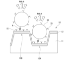
- FIG. 1 is a schematic diagram illustrating the principle of a method for measuring a target substance according to an embodiment.
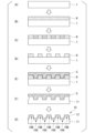
- FIG. 1 is a schematic diagram showing an example of a method for manufacturing a solid phase carrier used in a method for measuring a target substance according to an embodiment.
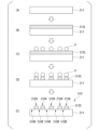
- FIG. 2 is a schematic diagram showing an example of a method for manufacturing a solid phase carrier used in a method for measuring a target substance according to an embodiment.
- FIG. 1 is a schematic diagram showing an example of a method for manufacturing a solid phase carrier used in a method for measuring a target substance according to an embodiment.
- FIG. 1 is a schematic diagram showing an example of a method for manufacturing a solid phase carrier used in a method for measuring a target substance according to an embodiment.
- FIG. 1 is a schematic diagram showing an example of a method for manufacturing a solid phase carrier used in a method for measuring a target substance according to an embodiment.
- FIG. 1 is a schematic diagram showing an example of a method for manufacturing a solid phase carrier used in
- 1 is a schematic diagram showing an example of a method for manufacturing a solid phase carrier used in a method for measuring a target substance according to an embodiment.
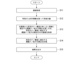
- 2 is a flowchart showing the flow of processing after acquisition of a scattered light image in a method for measuring a target substance according to an embodiment.
- 2 is a flowchart showing the flow of processing after acquisition of a scattered light image in a method for measuring a target substance according to an embodiment.
- 1 shows a configuration example of a target substance measurement system according to an embodiment. Scattered light from nanohole structure-bound particles and non-nanohole structure-bound particles when labeled nanoparticles are bonded to the nanostructure surface using a channel-type solid phase carrier device (1) having a nanohole structure as a predetermined nanostructure. The spectrum is shown.
- a dark-field microscopic image is shown when labeled nanoparticles are bonded to the nanostructure surface using a channel type solid phase carrier device (1) having a nanohole structure as a predetermined nanostructure.
- B Shows an image in which only the red spectrum (600 to 700 nm) was extracted from the dark-field microscope image in (A) using image processing software (ImageJ).
- C An image obtained by subtracting the image (B) from the image (A) and extracting only bright spots originating from the green spectrum (500 to 600 nm) is shown.
- the term “comprise” means that components other than the target component may be included.
- the term “consist of” means that no components other than the component in question are included.
- the term “consist essentially of” does not include components other than the target component in a manner that exerts a special function (such as a manner in which the effect of the invention is completely lost). means.
- the term “comprises” includes both “consist of” and “consist essentially of” aspects.
- Proteins, antibodies, peptides, polynucleotides (DNA, RNA), extracellular vesicles (exosomes, etc.), and cells can be isolated.
- isolated means in its natural state or separated from other components.
- isolated may be substantially free of other components.
- substantially free of other components means that the content of other components contained in the isolated component is negligible.
- the content of other components contained in the isolated component is, for example, 10% by mass or less, 5% by mass or less, 4% by mass or less, 3% by mass or less, 2% by mass or less, 1% by mass or less, 0. It can be up to 5% by weight, or up to 0.1% by weight.
- Proteins, antibodies, peptides, polynucleotides (DNA, RNA), extracellular vesicles (such as exosomes), and cells described herein refer to isolated proteins, isolated antibodies, isolated proteins, respectively.
- Specific binding substance means a substance that specifically binds to a specific biomolecule. "Bind specifically” means having high binding affinity for a particular biomolecule, but having very low binding affinity for other biomolecules. A specific binding substance preferably has a high binding property to a specific biomolecule, but has little binding property to other biomolecules.
- Combinations of biomolecules and specific binding substances include, for example, peptides or proteins and antibodies; nucleic acids and nucleic acids containing sequences complementary to the sequences contained in the nucleic acids; ligands and their receptors; enzymes and their substrates. , inhibitors or cofactors; sugar chains, lectins; peptides, proteins, nucleic acids, etc.; aptamers; transcription control sequence portions of nucleic acids and transcription control factors thereof; and the like, but are not limited to these.
- the target substance is an extracellular vesicle such as an exosome
- the specific binding substance that binds to the target substance may be a substance that specifically binds to a membrane protein of the extracellular vesicle.
- Antibody means an immunoglobulin that has antigen-binding activity.
- the antibody does not need to be an intact antibody as long as it has antigen-binding activity, and may be an antigen-binding fragment.
- the term "antibody” includes antigen-binding fragments.
- An "antigen-binding fragment” is a polypeptide that includes a portion of an antibody and maintains the antigen-binding properties of the original antibody.
- the antigen-binding fragment contains all six complementarity determining regions (CDRs) of the original antibody. That is, it is preferable to include all of CDR1, CDR2, and CDR3 of the heavy chain variable region and CDR1, CDR2, and CDR3 of the light chain variable region.
- CDRs complementarity determining regions
- Examples of antigen-binding fragments include Fab, Fab', F(ab') 2 , variable region fragment (Fv), disulfide bond Fv, single chain Fv (scFv), sc(Fv) 2,
- Antibodies may be derived from any organism. Examples of organisms from which antibodies are derived include, but are not limited to, mammals (humans, mice, rats, rabbits, horses, cows, pigs, monkeys, dogs, etc.), birds (chickens, ostriches), and the like. Antibodies may be of any class and subclass of immunoglobulin. The antibody may be a monoclonal antibody or a polyclonal antibody, but a monoclonal antibody is preferred. Antibodies can be produced by known methods such as immunization, hybridoma methods, and phage display methods.
- Target substance means the substance to be measured.
- the target substance is not particularly limited as long as it has a specific binding substance that specifically binds to the target substance.
- target substances include, but are not limited to, exosomes, peptides, proteins, nucleic acids, sugar chains, lectins, and lipids.
- the target substance may be contained in, for example, a biological sample.
- the biological sample is not particularly limited, and a sample collected from a living body can be used.
- Biological samples include, for example, body fluid samples such as blood, serum, plasma, saliva, urine, tears, sweat, milk, nasal discharge, semen, pleural effusion, gastrointestinal secretions, cerebrospinal fluid, interstitial fluid, and lymph, and cells. Examples include, but are not limited to, crushed samples and cell extract samples.
- the biological sample may be one obtained by extracting or concentrating a specific biological material fraction.
- a first aspect of the present invention is a method for measuring a target substance.
- the measurement method of this aspect is directed to nanoparticles capable of exciting surface plasmon resonance, the nanoparticles having a peak in the visible light region based on Mie scattering theory when irradiated with visible light.
- the predetermined nanostructure is one that changes the scattered light spectrum of the nanoparticles when the nanoparticles are bonded to the predetermined nanostructure, and the predetermined nanostructure has a structure in which the target substance is attached to the surface of the nanostructure.
- a solid phase carrier to which a second specific binding substance that specifically binds is bound is used.
- the second specific binding substance, the target substance, the first specific binding substance, and the nanoparticle are bound to the nanostructure surface in this order.
- the method of this aspect is directed to the solid phase carrier to which the target substance and the nanoparticle are sequentially bound via the second specific binding substance and the first specific binding substance.
- the target substance is bound between the nanoparticle and the solid phase carrier using the first specific binding substance and the second specific binding substance.
- light is irradiated onto the sandwich structure, and the scattered light spectrum of the nanoparticles that bind to the predetermined nanostructure and the scattered light spectrum of the nanoparticles that bind to a region that does not have the predetermined nanostructure are determined. identifying and counting the nanoparticles that bind to the nanostructures based on the difference.
- FIG. 1 is a schematic diagram illustrating the outline of the method of this embodiment.
- the solid phase carrier 10 has a nanostructure surface including a predetermined nanostructure 10A and a region 10B other than the nanostructure 10A.
- a second specific binding substance 15 is bound to the nanostructure surface.
- the target substance A is brought into contact with the nanostructure surface, the target substance A is captured by the second specific binding substance 15 (hereinafter also referred to as "step (i)").
- step (i) the second specific binding substance 15
- the labeled nanoparticles 20 on which the first specific binding substance 25 is immobilized are brought into contact with the nanostructure surface, the first specific binding substance 25 binds to the target substance A.
- step (ii) the labeled nanoparticles 20 bind to the nanostructure surface via the second specific binding substance 15, the target substance A, and the first specific binding substance 25 (hereinafter referred to as "step (ii)"). ).
- a structure is formed in which the labeled nanoparticles 20 are bound to the nanostructure surface of the solid phase carrier 10 via the second specific binding substance 15, the target substance A, and the first specific binding substance 25.
- This structure is a sandwich structure in which the target substance A is bound between the solid phase carrier 10 and the labeled nanoparticles 20 via the second specific binding substance 15 and the first specific binding substance 25. . In the sandwich structure in FIG.
- a second specific binding substance 15, a target substance A, a first specific binding substance 25, and a labeled nanoparticle 20 are sequentially placed on the nanostructure surface of a solid phase carrier 10. It has a connected structure.
- the labeled nanoparticles 20 bound to the nanostructure surface are bound to either the predetermined nanostructure 10A or the region 10B other than the nanostructure 10A.
- surface plasmon resonance is excited and a predetermined scattered light is generated.
- the nanostructure 10A has a nanostructure that changes the scattered light spectrum of the labeled nanoparticle 20 when the labeled nanoparticle 20 is bound thereto.
- the labeled nanoparticles 20 that bind to the nanostructure 10A generate scattered light of a different wavelength from those of the labeled nanoparticles 20 that bind to the region 10B. Therefore, the labeled nanoparticles 20 bonded to the nanostructure 10A are identified and counted based on the difference in the wavelength of the scattered light (hereinafter referred to as "step (iii)").
- the number of labeled nanoparticles 20 that bind to the nanostructure 10A shows a positive correlation with the concentration of the target substance in the sample. Therefore, by counting the labeled nanoparticles 20 that bind to the nanostructures 10A, the target substance in the sample can be measured.
- labeled nanoparticles capable of exciting surface plasmon resonance.
- the labeled nanoparticles have a particle size that, when irradiated with visible light, produces a scattered light spectrum having a peak in the visible light region based on Mie scattering theory. Further, a first specific binding substance that specifically binds to the target substance is bound to the labeled nanoparticle.
- Nanoparticles refer to particles having a particle size on the nanometer order (1 to 1000 nm).
- Nanoparticles capable of exciting surface plasmon resonance refer to nanoparticles having a size and material that can excite surface plasmon resonance when the nanoparticles are irradiated with light.
- Surface plasmon resonance is a phenomenon that occurs when light is incident on a conductive material, and the electric field oscillation of the incident light and the collective oscillation of free electrons of the conductive material combine at or near the surface of the conductive material. This refers to the propagation phenomenon of surface plasmon polaritons.
- Surface plasmon resonance is generally a collective oscillation phenomenon of conduction band electrons propagating along the interface between a metal with a negative dielectric function and a medium with a positive dielectric function.
- Surface plasmon resonance can be classified into propagating surface plasmon resonance, which is observed at the interface between a metal thin film and a dielectric, and localized surface plasmon resonance, which is observed at the surface of nanoparticles or nanostructures.
- “Nanoparticles capable of exciting surface plasmon resonance” may be nanoparticles capable of exciting localized surface plasmon resonance.
- the labeled nanoparticle includes a substance capable of exciting surface plasmon resonance on at least a portion of its surface.
- a substance capable of exciting surface plasmon resonance refers to, for example, a substance that has free electrons.
- a substance that can excite surface plasmon resonance is, for example, a substance that has a complex refractive index that satisfies the relationship [real part (n) ⁇ extinction coefficient (k)] with respect to incident light.
- the complex refractive index is the refractive index of an absorbing substance.
- the complex refractive index (m) can be expressed by the following formula.
- the real part n represents a normal refractive index
- the imaginary part k is called an extinction coefficient.
- Examples of substances that can excite surface plasmon resonance include metals.
- Examples of the metal include gold, silver, platinum, and aluminum.
- a portion of the surface of the labeled nanoparticle may be composed of a substance that can excite surface plasmon resonance, or the entire surface may be composed of a substance that can excite surface plasmon resonance.
- the entire particle of the labeled nanoparticle may be composed of a substance that can excite surface plasmon resonance, or a core that is composed of a substance that does not excite surface plasmon resonance and a shell that is composed of a substance that can excite surface plasmon resonance. It may also include.
- the labeled nanoparticle has a size capable of exciting surface plasmon resonance.
- the size that can excite surface plasmon resonance may be, for example, a size comparable to or smaller than the wavelength of light.
- the labeled nanoparticles have a particle size that, when irradiated with visible light, produces a scattered light spectrum having a peak in the visible light region based on Mie scattering theory.
- visible light refers to electromagnetic waves in the wavelength range of 360 to 830 nm.
- “Visible light region” refers to a wavelength region of 360 to 830 nm.
- the labeled nanoparticles may have a particle size of, for example, 10 nm to 300 nm, preferably 100 nm to 150 nm.
- the particle size means the average particle size on a number basis.
- the shape of the labeled nanoparticles is not particularly limited as long as it can have a peak of the scattered light spectrum in the visible light region when irradiated with visible light.
- the shape of the labeled nanoparticles includes, for example, a spherical shape, a cube shape, an arcine shape, a rod shape, a triangular pyramid shape, and the like.
- a first specific binding substance that specifically binds to the target substance is bound to the labeled nanoparticle.
- the first specific binding substance is appropriately selected depending on the target substance.
- the target substance is a peptide or protein
- an antibody that specifically binds to the peptide or protein can be used as the first specific binding substance.
- the target substance is a nucleic acid such as DNA or RNA
- a nucleic acid probe polynucleotide probe or oligonucleotide probe having a sequence complementary to the DNA or RNA may be used as the first specific binding substance. I can do it.
- the first specific binding substance can be bound to the labeled nanoparticles by a known method. For example, methods that utilize physical adsorption, methods that modify the labeled nanoparticle surface with a functional group that reacts with the functional group of the first specific binding substance (e.g., amino group modification, hydroxyl group modification, carboxy group modification, succinimide (group modification, etc.), a method using biotin-avidin bonding, etc.
- the surface of labeled nanoparticles is modified with avidin or an avidin derivative (streptavidin, etc.)
- the first specific binding substance is modified with biotin
- the biotin-avidin bond is used to bind the labeled nanoparticles to the first specific binding substance.
- a target binding substance may also be bound.
- the surface of the labeled nanoparticles may be treated so that the first specific binding substance can bind thereto.
- the surface treatment method include wet type surface treatment using an acid or alkali, and chemical surface treatment in which a linker molecule having a functional group such as an amino group or a carboxy group is bonded to the terminal.
- the labeled nanoparticles may be subjected to blocking treatment for the purpose of reducing nonspecific adsorption.
- the blocking treatment can be performed, for example, after binding the first specific binding substance to the labeled nanoparticles. By performing the blocking treatment, the particle surface to which the first specific binding substance is not bound is blocked. Thereby, non-specific adsorption to labeled nanoparticles can be reduced.
- Blocking agents include, for example, biologically derived protein-based blocking agents commonly used in the field of biochemistry such as bovine serum albumin (BSA), casein, skim milk, and fish gelatin; polyethylene glycol (PEG), polyvinyl alcohol (PVA); ) and other synthetic polymer compounds.
- BSA bovine serum albumin
- PEG polyethylene glycol
- PVA polyvinyl alcohol
- One type of blocking agent may be used alone, or two or more types may be used in combination.
- PEG and a protein-based blocking agent may be used in combination.
- the labeled nanoparticles may be stored in a storage solution until used.
- the pH of the storage solution is desirably such that the zeta potential on the surface of the labeled nanoparticles becomes high (or low) and the labeled nanoparticles repel each other.
- the storage solution does not contain molecules having the effect of neutralizing ions (eg, salts such as NaCl and KCl).
- the storage solution may contain a surfactant from the viewpoint of suppressing nonspecific adsorption and aggregation. Examples of the surfactant include nonionic surfactants such as Tweem20.
- the concentration of the surfactant in the storage solution can be, for example, 0.01 to 1% by mass, preferably 0.05 to 0.5% by mass. Specific examples of the storage solution include those containing about 0.1% of a nonionic surfactant such as Tween 20.
- a solid phase carrier having a nanostructure surface on which a plurality of predetermined nanostructures are arranged is used.
- the predetermined nanostructure changes the scattered light spectrum of the labeled nanoparticles when the labeled nanoparticles bind thereto.
- a second specific binding substance that specifically binds to the target substance is bound to the nanostructure surface.
- Nanostructure refers to a three-dimensional structure in which the structural unit is on the order of nanometers (1 to 1000 nm). In the nanostructure, the longest side of a virtual circumscribed rectangular parallelepiped that can accommodate the nanostructure may be on the order of nanometers.
- Nanostructured surface refers to the surface of a solid support having nanostructures.
- the solid phase carrier has a nanostructure surface on which a predetermined nanostructure (hereinafter referred to as "nanostructure (A)”) is arranged, which changes the scattered light spectrum of the labeled nanoparticle by binding the labeled nanoparticle.
- nanostructure (A) a predetermined nanostructure
- a second specific binding substance is immobilized on the nanostructured surface of the solid phase carrier, and a bond between the second specific binding substance, the target substance, and the first specific binding substance is formed.
- the labeled nanoparticles can then bind to the nanostructure surface.
- the state of localized surface plasmon resonance excited by light irradiation changes, and the scattered light spectrum of the labeled nanoparticles changes.
- the nanostructure (A) has a shape and material that changes the scattered light spectrum of the labeled nanoparticles when the labeled nanoparticles are bound thereto.
- the nanostructure (A) includes a substance capable of exciting surface plasmon resonance on at least a portion of its surface.
- the substance that can excite surface plasmon resonance include the same substances as mentioned above.
- a part of the surface of the nanostructure (A) may be composed of a substance capable of exciting surface plasmon resonance, or the entire surface may be composed of a substance capable of exciting surface plasmon resonance.
- the entire structure of the nanostructure (A) may be made of a substance that can excite surface plasmon resonance, and a layer that is made of a substance that does not excite surface plasmon resonance is provided with a substance that can excite surface plasmon resonance. It may be a stack of layers made up of.
- a part of the structure including a part of the surface may be made of a substance that can excite surface plasmon resonance.
- the shape of the nanostructure (A) is not particularly limited as long as it changes the scattered light spectrum of the labeled nanoparticles by binding the labeled nanoparticles.
- Examples of the shape of the nanostructure (A) include pit shape, hole shape, cone shape, spherical shape, donut shape, and the like.
- the size of the nanostructure (A) is not particularly limited as long as it changes the scattered light spectrum of the labeled nanoparticles by binding the labeled nanoparticles. In image processing, it is easier to extract the scattered light of the labeled nanoparticles bound to the nanostructure (A).
- the particles are of a size that allows them to bond.
- the longest side of a virtual circumscribed rectangular parallelepiped that can accommodate the nanostructure (A) is 0.2 times or more and less than 2 times the particle size of the labeled nanoparticle.
- a plurality of nanostructures (A) are arranged on the nanostructure surface of the solid support.
- the plurality of nanostructures (A) arranged on the nanostructure surface are all the same nanostructure.
- the nanostructures (A) are arranged in a periodic array on the nanostructure surface of the solid phase support, since it becomes easier to extract the scattered light of the labeled nanoparticles bound to the nanostructures (A). It is preferable.
- Period arrangement means that the nanostructures (A) are arranged at a constant period. Examples of the periodic arrangement of the nanostructures (A) include a lattice arrangement.
- the nanostructure surface of the solid phase support may or may not have a structure other than the nanostructure (A).
- the surface of the nanostructure preferably does not have any nanostructures other than the nanostructure (A) because it becomes easier to extract the scattered light of the labeled nanoparticles bound to the nanostructure (A).
- the solid phase support may be one in which nanostructures (A) are formed on the surface of a substrate.
- the material of the substrate is not particularly limited.
- the substrate is made of, for example, a dielectric material. Examples of the material of the substrate include, but are not limited to, glass, silicon, and plastic resin.
- Figures 2 to 6 show examples of methods for producing solid phase carriers.
- FIG. 2 is an example of manufacturing a solid phase carrier using a lithography method.
- the surface of the substrate is polished and cleaned to produce a stamper substrate 1 having a smooth surface (FIG. 2(A)).
- a resist film R is formed on the surface of the stamper substrate 1 (FIG. 2(B)).
- the resist film R may be formed of either a positive resist or a negative resist.
- the resist can be selected as appropriate depending on the nanostructure (A) to be produced.
- the resist film R can be formed by a known method such as a spin coating method.
- a pattern is drawn on the resist film R (FIG. 2(C)).
- a known method can be used for drawing the pattern. Examples of the pattern drawing method include electron beam drawing, laser drawing, and the like.
- the pattern can be formed as appropriate depending on the arrangement of the nanostructures (A).
- the nanostructures (A) are arranged in a periodic manner, a pattern is drawn in accordance with the periodic arrangement.
- the resist film R is developed (FIG. 12(D)).
- the resist film in the exposed portion is removed to form a resist pattern.
- the resist film in non-exposed areas is removed to form a resist pattern.
- a stamper S having an inverted uneven shape is produced by electroforming (plating) (FIG. 2(E)).
- the substrate 11 is molded using the stamper S as a mold (FIG. 2(F)).
- the stamper S it is possible to produce a plurality of substrates 11.
- an injection molding method, a nanoimprint method, etc. can be used as appropriate.
- the base material and the nanostructure on the substrate surface can be made of different materials.
- a thin film 12 of a substance capable of exciting surface plasmon resonance is formed on the surface of the substrate 11 (FIG. 2(G)).
- a solid phase carrier 10 having a nanostructure surface having a nanostructure 10A, which is the nanostructure (A), and a region 10B other than the nanostructure (A).
- FIG. 3 is an example of manufacturing a solid phase carrier using nanoparticles.
- the surface of the substrate is polished and cleaned to produce a substrate 111 having a smooth surface (FIG. 3A).
- nanoparticles 112 made of a substance capable of exciting surface plasmon resonance are applied onto the substrate 111 (FIG. 3(B)).
- the nanoparticles 112 can have a size such that when irradiated with visible light, a scattered light spectrum having a peak in the visible light region is generated based on Mie scattering theory.
- the particle size of the nanoparticles 112 is, for example, 10 nm to 300 nm.
- the shape of the nanoparticles 112 examples include a spherical shape, a cube shape, an arcine shape, a rod shape, and a triangular pyramid shape.
- the method for applying the nanoparticles 112 is not particularly limited, and a known method can be used.
- the nanoparticles 112 can be applied to the substrate 111 by dropping a dispersion of the nanoparticles 112 prepared by dispersing the nanoparticles 112 in a solvent onto the surface of the substrate 111 and drying.
- the dispersion of nanoparticles 112 can be applied to the substrate 111 using a spin coating method. The type of solvent, the concentration of the nanoparticles 112, the drying time, etc.
- the rotation speed, rotation time, etc. of the substrate 111 can be adjusted as appropriate. In this way, it is possible to obtain a solid phase carrier 110 having a nanostructure surface having a nanostructure 110A, which is the nanostructure (A), and a region 110B other than the nanostructure (A).
- FIG. 4 shows an example of manufacturing a solid phase carrier using a substrate on which a thin film of a substance capable of exciting surface plasmon resonance is formed.
- the surface of the substrate is polished and cleaned to produce a substrate 211 having a smooth surface (FIG. 4A).
- a thin film 212L of a substance capable of exciting surface plasmon resonance is formed on the surface of the substrate 211 (FIG. 4(B)).
- the thin film 212L can be formed using a known method. Examples of the method for forming the thin film 212L include a vacuum film forming method (sputtering method, vacuum evaporation method, etc.), a spin coating method, and the like.
- the thickness of the thin film 212L can be, for example, 10 to 300 nm, 20 to 200 nm, or 40 to 100 nm.
- nanoparticles 212P made of a substance capable of exciting surface plasmon resonance are applied to the surface of the thin film 212L (FIG. 4(C)).
- the method for applying the nanoparticles 212P includes a method similar to the method for applying the nanoparticles 112 in the method shown in FIG. In this way, it is possible to obtain a solid phase carrier 210 having a nanostructure surface having a nanostructure 210A which is the nanostructure (A) and a region 210B other than the nanostructure (A).
- the thin film formed on the surface of the substrate 211 may be a thin film of a substance that does not excite surface plasmon resonance.
- the thin film may be formed of resin.
- the resin used for forming the thin film is not particularly limited, and examples thereof include acrylic resin, polyolefin, cycloolefin polymer, cycloolefin copolymer, epoxy resin, phenol resin, polystyrene, polydimethylsiloxane (PDMS), and the like.
- FIG. 5 is an example of manufacturing a solid phase carrier using an etching method.
- the surface of the substrate is polished and cleaned to produce a substrate 311 having a smooth surface (FIG. 5A).
- a thin film 312L of a substance capable of exciting surface plasmon resonance is formed on the surface of the substrate 311 (FIG. 5(B)).
- the thin film 312L can be formed using a known method. Examples of the method for forming the thin film 312L include a vacuum film forming method (sputtering method, vacuum evaporation method, etc.), a spin coating method, and the like.
- the thickness of the thin film 312L is not particularly limited, but can be selected depending on the particle size of the labeled nanoparticles.
- the thickness of the thin film 312L can be, for example, 10 to 300 nm, 20 to 200 nm, or 40 to 100 nm.
- nanoparticles P are applied to the surface of the thin film 312L (FIG. 5(C)).
- the material of the nanoparticles P is not particularly limited, and any desired material can be used.
- the nanoparticles P for example, resin beads or the like (eg, polystyrene beads) can be used.
- the particle size of the nanoparticles P can be appropriately selected depending on the size of the nanostructure (A) to be finally formed.
- the particle size of the nanoparticles P can be, for example, 0.2 times or more and less than 2 times the particle size of the labeled nanoparticles.
- the nanoparticles P As a method for applying the nanoparticles P, a method similar to the method for applying the nanoparticles 112 in the method shown in FIG. 3 can be mentioned.
- a specific example of the nanoparticles P is polystyrene beads with a particle size of 100 nm.
- the thin film 312L is etched by an etching process using the nanoparticles P as a mask (FIG. 5(D)).
- a structure 312C made of a substance capable of exciting surface plasmon resonance is formed.
- the etching process may be dry etching such as reactive ion etching, or wet etching using acid, alkali, or the like.
- Etching conditions can be appropriately selected depending on the shape and material of the nanostructure (A) to be finally produced.
- the nanoparticles (P) are removed (FIG. 5(E)).
- the method for removing nanoparticles (P) is not particularly limited.
- An example of a method for removing nanoparticles (P) is ultrasonication. In this way, it is possible to obtain a solid phase carrier 310 having a nanostructure surface having a nanostructure 310A, which is the nanostructure (A), and a region 310B other than the nanostructure (A).
- a 50 nm thin gold film is formed on a glass substrate by sputtering, polystyrene beads with a diameter of 100 nm are applied by spin coating, the gold thin film is etched with Ar gas using the polystyrene beads as a mask, and then the polystyrene beads are exposed to ultrasonic waves. removed by processing.
- a solid phase support having a nanostructured surface on which 100 nm gold nanostructures are arranged can be produced on a glass substrate.
- FIG. 6 is an example of manufacturing a solid phase support by combining a lithography method and an etching method.
- a substrate 411 having a smooth surface is manufactured by polishing and cleaning the surface of the substrate (FIG. 6A).
- a thin film 412L of a substance capable of exciting surface plasmon resonance is formed on the surface of the substrate 411 (FIG. 6(B)).
- the method for forming the thin film 412L and its thickness may be the same as that for the thin film 312L in the method shown in FIG.
- a resist film R is formed on the surface of the thin film 412L (FIG. 6(C)).
- a pattern is drawn on the resist film R (FIG. 6(D)).
- the resist film R is developed (FIG. 6(E)).
- the resist film in the exposed portion is removed to form a resist pattern.
- the resist film in non-exposed areas is removed to form a resist pattern.
- the thin film 412L is etched using the resist pattern as a mask (FIG. 6(F)).
- a structure 412C made of a substance capable of exciting surface plasmon resonance is formed.
- the resist film R is removed (FIG. 6(G)). In this way, it is possible to obtain a solid phase carrier 410 having a nanostructure surface having a nanostructure 410A, which is the nanostructure (A), and a region 410B other than the nanostructure (A).
- a second specific binding substance that specifically binds to the target substance is bound to the nanostructure surface of the solid phase carrier.
- the second specific binding substance is appropriately selected depending on the target substance.
- the second specific binding substance may be the same as or different from the first specific binding substance.
- the second specific binding substance is preferably different from the first specific binding substance.
- the first specific binding substance and the second specific binding substance may be antibodies that bind to mutually different epitopes.
- the first specific binding substance and the second specific binding substance are nucleic acid probes (polynucleotide probes or oligonucleotide probes) that hybridize to different regions. There may be.
- the second specific binding substance can be bound to the nanostructured surface of the solid phase support by a known method.
- Examples of the method for binding the second specific binding substance to the nanostructure surface include the same methods as those mentioned as the method for binding the first specific binding substance to the labeled nanoparticles.
- the nanostructured surface of the solid phase support may be subjected to surface treatment.
- Surface treatments include, for example, optical treatment such as ultraviolet treatment, plasma treatment, wet type treatment with acid or alkali, chemical treatment to bond linker molecules having a functional group such as an amino group or a carboxy group at the end, etc. can be mentioned.
- the second specific binding substance may be bound to the nanostructure surface by forming a structure on the nanostructure surface of the solid phase support in which a reaction solution containing the second specific binding substance can be retained. .
- a reaction solution containing the second specific binding substance for example, by retaining the reaction solution containing the second specific binding substance for a certain period of time in a structure in which the reaction solution on the nanostructure surface can be retained, the binding reaction of the second specific binding substance to the nanostructure surface can be performed. It can be performed.
- the structure in which the reaction solution can be kept include a well structure, a channel structure, and the like.
- the well structure can be formed, for example, by laminating a resin sheet or the like having through holes of a desired size on the surface of the nanostructure.
- the channel structure can be formed, for example, by arranging a resin sheet so that a channel is formed on the surface of the nanostructure, and closing the upper part of the channel with another resin sheet.
- the material of the resin sheet is not particularly limited, and examples thereof include PDMS, cycloolefin polymer, cycloolefin copolymer, and the like.
- the binding reaction of the second specific binding substance to the nanostructure surface may be carried out at room temperature (20 to 30°C) or may be carried out in a constant temperature bath maintained at a predetermined temperature. The temperature of the binding reaction can be appropriately selected depending on the type of the second specific binding substance.
- the nanostructured surface of the solid phase support may be subjected to blocking treatment for the purpose of reducing nonspecific adsorption.
- the blocking treatment can be performed, for example, after binding the second specific binding substance to the nanostructure surface of the solid phase carrier. By performing the blocking treatment, the nanostructure surface to which the second specific binding substance is not bound is blocked. Thereby, non-specific adsorption to the nanostructure surface can be reduced.
- the blocking agent the same ones as those mentioned above as the blocking agent for the labeled nanoparticles can be mentioned.
- the nanostructured surface of the solid phase support may be subjected to a cleaning treatment.
- the washing treatment can be performed, for example, after binding the second binding substance to the nanostructure surface of the solid phase support and/or after the blocking treatment.
- the cleaning process can be performed by repeating the steps of supplying a cleaning liquid to the nanostructure surface and removing the cleaning liquid about 1 to 3 times.
- the washing solution include a buffer solution such as PBS (Phosphate-buffered saline) to which a nonionic surfactant such as Tween 20 is added.
- Step (i) is a step of binding the target substance to the nanostructure surface through binding with a second specific binding substance.
- Step (i) can be performed by bringing a sample that may contain the target substance into contact with the nanostructured surface of the solid support.
- the sample may be brought into contact with the nanostructured surface by forming a structure on the nanostructured surface of the solid support in which the sample can be placed.
- the sample can be brought into contact with the nanostructure surface by leaving the sample for a certain period of time in a structure in which the sample on the nanostructure surface can be placed.
- Examples of the structure in which the sample can be placed include a well structure, a channel structure, and the like.
- Conditions for the binding reaction between the second specific binding substance and the target substance can be selected as appropriate depending on the types of the target substance and the second specific binding substance.
- the reaction temperature include 20°C or higher, 30°C or higher, or 35°C or higher.
- the upper limit of the reaction temperature is not particularly limited, but may be, for example, 50°C or lower, 45°C or lower, or 40°C or lower.
- Examples of the reaction temperature range include 20 to 50°C, 30 to 45°C, or 30 to 40°C.
- the reaction time is not particularly limited, and can be set to a time that allows the binding reaction between the second specific binding substance and the target substance to sufficiently proceed.
- the reaction time can be appropriately selected depending on the type of target substance and second specific binding substance.
- the target substance is a protein or a peptide and the second specific target substance is an antibody
- examples of the reaction time include 3 minutes or more, 5 minutes or more, or 10 minutes or more.
- the upper limit of the reaction time is not particularly limited, and may be, for example, 60 minutes or less, 45 minutes or less, 30 minutes or less, or 20 minutes or less. Examples of the reaction time range include 3 to 60 minutes, 5 to 45 minutes, or 10 to 30 minutes.
- the sample may be appropriately diluted with a dilution buffer.
- the dilution buffer may contain a salt such as NaCl or KCl in order to lower the zeta potential (surface potential) and maintain reaction efficiency.
- a buffer containing salt PBS, etc.
- the dilution buffer may also contain a blocking agent and/or a surfactant (such as Tween 20) to reduce non-specific adsorption.
- the sample may be removed from the nanostructure surface and a cleaning process may be performed.
- a cleaning process By performing the cleaning treatment, unreacted impurities remaining on the nanostructure surface can be removed.
- the cleaning process can be performed by repeating the steps of supplying a cleaning liquid to the nanostructure surface and removing the cleaning liquid about 1 to 3 times.
- the cleaning liquid the same ones as mentioned above can be mentioned.
- Step (ii) is a step of binding labeled nanoparticles to the surface of the nanostructure through binding between the target substance and the first binding substance.
- Step (ii) can be performed by bringing a dispersion containing labeled nanoparticles into contact with the nanostructure surface of the solid support.
- the labeled nanoparticle dispersion may be brought into contact with the nanostructured surface by forming a structure on the nanostructured surface of the solid support in which a sample can be retained.
- the labeled nanoparticle dispersion can be brought into contact with the nanostructure surface by leaving the sample in a structure capable of retaining the labeled nanoparticle dispersion on the nanostructure surface for a certain period of time.
- Examples of the structure in which the labeled nanoparticle dispersion can be placed include a well structure, a channel structure, and the like.
- the first specific binding substance that binds to the labeled nanoparticles binds to the target substance captured by the second specific binding substance.
- the labeled nanoparticles can be bound to the nanostructure surface through binding with the second specific binding substance, the target substance, and the first specific binding substance.
- the labeled nanoparticle dispersion may contain a salt such as NaCl or KCl in order to lower the zeta potential (surface potential) and maintain reaction efficiency.
- a salt such as NaCl or KCl
- PBS buffer containing salt
- the labeled nanoparticle dispersion may contain a blocking agent and/or a surfactant (such as Tween 20) in order to reduce non-specific adsorption.
- Conditions for the binding reaction between the first specific binding substance and the target substance can be selected as appropriate depending on the types of the target substance and the first specific binding substance.
- the reaction temperature include 20°C or higher, 30°C or higher, or 35°C or higher.
- the upper limit of the reaction temperature is not particularly limited, but may be, for example, 50°C or lower, 45°C or lower, or 40°C or lower.
- Examples of the reaction temperature range include 20 to 50°C, 30 to 45°C, or 30 to 40°C.
- the reaction time is not particularly limited, and can be set to a time that allows the binding reaction between the first specific binding substance and the target substance to sufficiently proceed.
- the reaction time can be appropriately selected depending on the type of target substance and first specific binding substance.
- the target substance is a protein or a peptide and the first specific target substance is an antibody
- examples of the reaction time include 3 minutes or more, 5 minutes or more, or 10 minutes or more.
- the upper limit of the reaction time is not particularly limited, and may be, for example, 60 minutes or less, 45 minutes or less, 30 minutes or less, or 20 minutes or less. Examples of the reaction time range include 3 to 60 minutes, 5 to 45 minutes, or 10 to 30 minutes.
- the labeled nanoparticle dispersion liquid may be removed from the nanostructure surface and a washing process may be performed.
- a washing process By performing the cleaning treatment, unreacted impurities remaining on the nanostructure surface can be removed.
- the cleaning process can be performed by repeating the steps of supplying a cleaning liquid to the nanostructure surface and removing the cleaning liquid about 1 to 3 times.
- the cleaning liquid the same ones as mentioned above can be mentioned.
- step (i) and step (ii) the target substance is bound to the nanostructure surface via the second specific binding substance, and the first specific binding substance that binds to the labeled nanoparticle is bound to the second specific binding substance.
- a solid phase support can be obtained that is bound to a target substance that binds to a specific binding substance. That is, in the solid phase carrier after step (i) and step (ii), the target substance is bonded to the second specific binding substance and the first specific binding substance between the nanostructure surface of the solid phase carrier and the labeled nanoparticle. It has a sandwich structure that is bonded via a binding substance. In this sandwich structure, a second specific binding substance, a target substance, a first specific binding substance, and a labeled nanoparticle are bound in this order to the nanostructure surface of a solid support. It has become.
- Step (iii)> In the solid phase carrier, the target substance is bound to the nanostructured surface via a second specific binding substance, and the nanoparticles have the second specific binding substance, the target substance, and the first bonded to the nanostructured surface. It is preferable that the compound is bound to the compound via a specific binding substance.
- the nanostructure surface of this solid phase support is irradiated with light, and the scattered light spectrum of the labeled nanoparticles bonded to the predetermined nanostructure (nanostructure (A)) and the predetermined nanostructure (nanostructure (A)) are detected. Labeled nanoparticles that bind to the nanostructure (nanostructure (A)) are identified and counted based on the difference between the scattered light spectrum of the labeled nanoparticle that binds to a region that does not have (A)).
- the light irradiated onto the nanostructure surface of the solid phase support is visible light.
- the labeled nanoparticles bonded to the nanostructure surface generate scattered light.
- labeled nanoparticles bound to the nanostructure surface can be detected.
- the surface plasmon resonance state of the labeled nanoparticles bound to the nanostructure (A) changes due to the nanostructure (A), and the scattered light spectrum changes. Therefore, the labeled nanoparticles that bind to the nanostructure (A) generate a scattered light spectrum (hereinafter also referred to as "scattered light spectrum (A)”) specific to the nanostructure (A).
- labeled nanoparticles that bind to a region that does not have a nanostructure (A) (hereinafter also referred to as "region (B)") generate a scattered light spectrum that is different from the scattered light spectrum (A). If region (B) does not have a nanostructure that changes the scattered light spectrum of the labeled nanoparticle, the labeled nanoparticle bound to region (B) will have the same scattered light spectrum as that generated by the labeled nanoparticle alone. Generate a spectrum. When the region (B) has a nanostructure (a structure different from the nanostructure (A)) that changes the scattered light spectrum of the labeled nanoparticle, the labeled nanoparticle bound to the region (B) is unique to the nanostructure.
- the light source of the irradiation light is not particularly limited.
- the irradiation light source include a halogen lamp, an LED lamp, and a laser light source.
- the irradiation light source can be appropriately selected depending on the scattered light spectrum generated from the labeled nanoparticles. For example, a microscope with dark field optical system can be used.
- the scattered light spectrum generated from the labeled nanoparticles can be detected with a detector equipped with a light receiving element, such as a CCD camera or a CMOS camera.
- a light receiving element such as a CCD camera or a CMOS camera.
- a highly sensitive light receiving element such as a photomultiplier tube (PMT) or EM-CCD may be used.
- An optical filter that transmits or blocks specific wavelengths may be used between the solid phase carrier and the light receiving element.
- an optical filter may be used between the solid phase carrier and the light receiving element to block the peak wavelength of the scattered light spectrum generated by the labeled nanoparticles bound to the region (B).
- an optical filter that transmits only the peak wavelength of the scattered light spectrum generated by the labeled nanoparticles bonded to the nanostructure (A) may be used between the solid phase carrier and the light receiving element.
- FIG. 7 is a flowchart showing the flow of processing after image acquisition. After acquiring the image in S11, the image undergoes hue separation using RGB information, HSV information, etc. (S12). Next, a bright spot originating from the scattered light of the labeled nanoparticles bound to region (B) is subtracted from the original image.
- an image of only bright spots originating from the scattered light of the labeled nanoparticles bonded to the nanostructure (A) is obtained (S13).
- bright spots of labeled nanoparticles bonded to the nanostructure (A) are counted from the image acquired in S13 (S14).
- the counting result is output (S15) and the process ends.
- an image may be obtained by extracting only the bright spots originating from the scattered light of the labeled nanoparticles bonded to the nanostructure (A) from the original image.
- FIG. 8 is a flowchart showing the flow of processing after image acquisition when an optical filter that transmits or blocks specific wavelengths is used between the solid phase carrier and the light receiving element.
- the image acquired in S21 is an image of only bright spots originating from the scattered light of the labeled nanoparticles bonded to the nanostructure (A).
- bright spots originating from the scattered light of the labeled nanoparticles bonded to the nanostructure (A) are counted from the image acquired in S21 (S22).
- the counting result is output (S23) and the process ends.
- the coordinate information of the periodic arrangement is used in image processing to detect the scattered light of the labeled nanoparticles that bind to the region (B).
- the resulting bright spot may be removed.
- only the bright spots originating from the scattered light of the labeled nanoparticles bonded to the nanostructure (A) may be extracted using the coordinate information of the periodic array.
- a method may be used in which statistical processing based on Poisson distribution is used to improve the counting accuracy of a very small number. It is also possible to comprehensively quantify the target substance by performing counting in a plurality of observation fields and using the total value, average value, or other statistical method. By using statistical processing of Poisson distribution, the target substance may be quantified with a relatively small observation field.
- a target substance is captured using a solid phase carrier having a nanostructure surface on which a predetermined nanostructure that changes the scattered light spectrum of the labeled nanoparticle is arranged, and the labeled nanoparticle is attached to the nanostructure surface.
- a second aspect of the present invention is a target substance measurement system used in the target substance measurement method of the first aspect.
- the target substance measurement system of this aspect includes: a light source that irradiates light to the nanoparticles bound to the solid phase carrier; a detector that detects scattered light from the nanoparticles; Based on the scattered light image, based on the difference between the scattered light spectrum of the nanoparticles that bind to the predetermined nanostructure and the scattered light spectrum of the nanoparticles that bind to a region that does not have the predetermined nanostructure, and a counting unit that identifies and counts the nanoparticles bound to a predetermined nanostructure.
- FIG. 9 is a diagram showing an example of the configuration of a target substance measurement system.
- the target substance measurement system 100 includes a light source 40, a detector 30, an arithmetic device 50, and an output device 60.
- the light source 40 is a light source that irradiates the labeled nanoparticles 20 bonded to the nanostructure surface of the solid phase carrier 10 with light.
- Examples of the light source include those exemplified above.
- a light source of a microscope with a dark field optical system may be used.
- the labeled nanoparticles 20 may be bonded to the nanostructure surface via a second specific binding substance, a target substance, and a first specific binding substance (not shown).
- the bonding structure between the solid phase carrier 10 and the labeled nanoparticles 20 may be the same as that shown in FIG. 1.
- the detector 30 detects scattered light from the labeled nanoparticles 20 bonded to the nanostructure surface of the solid phase support 10.
- the detector 30 can include a light receiving element 31, a filter 32, and a lens 33.
- the light receiving element 31 may be any element as long as it can detect the scattered light from the labeled nanoparticles 20. Examples of the light receiving element 31 include a CCD, CMOS, photomultiplier tube (PMT), and EM-CCD.
- the filter 32 a filter that transmits light of a specific wavelength or a filter that blocks light of a specific wavelength can be used.
- the filter 32 may be, for example, a filter that transmits the peak wavelength of the scattered light spectrum of the labeled nanoparticle 20 that binds to the nanostructure (A) (10A in FIG. 9). Alternatively, it may be a filter that blocks the peak wavelength of the scattered light spectrum of the labeled nanoparticles 20 that binds to the region (region (B): 10B in FIG. 9) that does not have the nanostructure (A).
- an objective lens can be used as the lens 33. The magnification of the objective lens is, for example, 50 to 100 times.
- the arithmetic device 50 includes a processor such as a CPU and a memory, and executes image processing of the image acquired by the detector 30.
- the computing device 50 includes a counting unit that identifies and counts labeled nanoparticles that bind to the nanostructure (A) from the scattered light image acquired by the detector 30.
- the scattered light image acquired by the detector 30 may be an image of only bright spots of scattered light originating from the labeled nanoparticles 20 bonded to the nanostructure (A).
- the counting unit can count the number of labeled nanoparticles 20 bonded to the nanostructure (A) by counting bright spots in the scattered light image acquired by the detector 30 (see FIG. 8).
- the scattered light image acquired by the detector 30 will show a bright spot of scattered light from the labeled nanoparticles 20 that binds to the nanostructure (A) and a region (B). It includes both a bright spot of scattered light from the labeled nanoparticle 20.
- the computing device 50 obtains an image in which only bright spots of scattered light from the labeled nanoparticles 20 bonded to the nanostructure (A) are extracted from the original image obtained by the detector 30. In the image acquired above, the number of labeled nanoparticles 20 bonded to the nanostructure (A) is counted by counting the bright spots (see FIG. 7).
- the arithmetic device 50 may be an external computer connected to the detector 30, or may be a computer built into a dark-field optical microscope device including the detector 30 and the light source 40.
- the external computer may be connected by wire or wirelessly, or may be connected to the detector 30 via a network such as the Internet or a communication line such as a telephone line.
- the output device 60 outputs various information such as the results counted by the counting section.
- the output device 60 includes, for example, a display device such as a CRT display, a liquid crystal display, or an organic EL display.
- the target substance measurement system of this aspect can be used to carry out the target substance measurement method of the first aspect.
- Example 1 (Preparation of solid phase carrier (1)) According to the method shown in FIGS. 2(A) to 2(F), a molded substrate (1) having a nanostructured surface in which nanoholes were formed in a periodic arrangement was produced.
- a cycloolefin polymer resin (Zeonor manufactured by Nippon Zeon) was used as the material for the molded substrate.
- the nanohole was an inverted truncated conical hole with a bottom diameter of 100 nm, an opening diameter of 160 nm, and a depth of 100 nm.
- the pitch of nanoholes was 500 nm.
- a thin gold film with a thickness of 50 nm was formed on the surface of the molded substrate using a vacuum sputtering method. In this way, a solid phase carrier (1) was obtained.
- channel type solid phase carrier device (1) Preparation of channel type solid phase carrier device (1)
- a 140 ⁇ m thick channel forming sheet manufactured by Microfluidic, model number 10001380
- a 100 ⁇ m thick cycloolefin polymer sheet was laminated and bonded to the flow path forming sheet.
- a channel type solid phase carrier device (1) was produced.
- the bottom surface of the channel is constituted by the nanostructured surface of the solid phase carrier (1).
- the flow path forming sheet and the flow path cover sheet are not limited to those described above, and any ones can be used. From the viewpoints of the reaction efficiency of the detection target substance, the amount of sample used, and aberrations in the optical detection method, it is preferable that the thickness of the flow path forming sheet and the flow path cover sheet be as small as possible.
- An anti-PSA antibody (manufactured by HyTest, model number 4P33-1H12) was diluted with PBS to prepare an anti-PSA antibody solution with a concentration of 5 ⁇ g/mL.
- a pad for example, Kimwipe, etc.
- 1 ⁇ L of the anti-PSA antibody solution was pipetted into the channel from the inlet of the channel.
- the anti-PSA antibody was placed in the channel and allowed to stand at room temperature for 10 minutes to allow the anti-PSA antibody to be adsorbed onto the nanostructure surface.
- 1 ⁇ L of PBS containing 0.05% Tween 20 was pipetted into the channel to remove unreacted anti-PSA antibody. This washing operation was repeated twice.
- a blocking solution was prepared by diluting BSA (bovine serum albumin, manufactured by Thermo Fisher, model number 37525) to 1% with PBS. 1 ⁇ L of blocking solution was poured into the channel using a pipette, and the mixture was allowed to stand at room temperature for 10 minutes. Next, 1 ⁇ L of PBS containing 0.05% Tween 20 was pipetted into the channel to remove unreacted BSA. This washing operation was repeated twice.
- BSA bovine serum albumin
- Anti-PSA antibody (manufactured by HyTest, model number 4P33-5A6) was bound to the surface of gold nanoparticles with a diameter of 150 nm (manufactured by Cytodiagnostics, model number G-150-100), and diluted with PBS containing 0.05% Tween 20.
- a labeled gold nanoparticle suspension with a concentration of 0.06 mg/mL (OD 0.5) was prepared.
- 1 ⁇ L of the labeled gold nanoparticle suspension was poured into the flow channel using a pipette, and left at room temperature for 10 minutes.
- 1 ⁇ L of PBS containing 0.05% Tween 20 was pipetted into the channel to remove unreacted labeled gold nanoparticles. This washing operation was repeated twice.
- the nanostructure surface within the channel was observed from above the channel type solid phase carrier device (1) using a dark field microscope (objective lens magnification of 50 times, NA 0.55). In a dark field microscope, only scattered light caused by substances and structures present on the sample surface is observed. Using a dark-field microscope, labeled gold nanoparticles bound to the nanostructure surface of the channel-type solid phase carrier device (1) via the antigen-antibody complex of anti-PSA antibody/PSA/anti-PSA antibody and nanoholes on the nanostructure surface were observed. Scattered light was observed. The coordinates of nanoholes on the nanostructure surface were determined from the scattered light spectrum generated by the nanohole structure.
- the color of the scattered light of gold nanoparticles (hereinafter referred to as “nanohole structure-bound particles”) at a position that matches the nanohole coordinates does not match the nanohole coordinates. It was confirmed that the color of scattered light of gold nanoparticles (hereinafter referred to as “non-nanohole structure-bound particles”) at different positions can be distinguished. Non-nanohole structure-bound particles were observed with red scattered light. Nanohole structure-bound particles were observed with green scattered light.
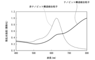
- FIG. 10 shows the results of measuring the scattered light spectra of nanohole structure-bound particles and non-nanohole structure-bound particles.
- the scattered light spectrum of the non-nanohole structure-bound particles had a peak at a wavelength of 600 nm to 700 nm.
- the scattered light spectrum of the nanohole structure-coupled particles had a peak at a wavelength of 500 nm to 600 nm.
- the scattered light spectra of both were significantly different from each other.
- the analyte and labeled gold nanoparticles were reacted in the same manner as above, except that the PSA concentration in the analyte sample was 1.0 ng/mL, 0.1 ng/mL, or 0 ng/mL, and the nanostructure surface
- the scattered light spectrum of labeled gold nanoparticles bound to was measured.
- an image (C) in which only bright spots originating from the green spectrum (500 nm to 600 nm) were extracted was obtained, and the number of bright spots was counted.
- Table 1 The results are shown in Table 1.
- Example 2 (Preparation of solid phase carrier (2))
- a stamper (A) was produced according to the method shown in FIGS. 2(A) to 2(E).
- the electroforming process was performed again to produce a stamper (B).
- a molded substrate (2) was produced using this stamper (B).
- the molded substrate (2) had a concavo-convex pattern reversed from that of the molded substrate (1) of Example 1, and had a nanostructured surface in which nanopits were formed in a periodic arrangement.
- a thin gold film with a thickness of 50 nm was formed on the surface of the molded substrate using a vacuum sputtering method. In this way, a solid phase carrier (2) was obtained.
- a channel type solid phase carrier device (2) was produced in the same manner as in Example 1 except that solid phase carrier (2) was used instead of solid phase carrier (1).
- the nanostructure surface within the channel was observed from above the channel type solid phase carrier device (2) using a dark field microscope (objective lens magnification of 50 times, NA 0.55).
- a dark-field microscope labeled gold nanoparticles bound to the nanostructured surface of the channel-type solid phase carrier device (2) via the antigen-antibody complex of anti-PSA antibody/PSA/anti-PSA antibody, and nanopits on the nanostructured surface were observed. Scattered light was observed. The coordinates of the nanopits on the nanostructure surface were determined from the scattered light spectrum generated by the nanopit structure.
- the color of the scattered light of gold nanoparticles (hereinafter referred to as “nanopit structure bonding particles”) at a position that matches the nanopit coordinates and the color that does not match the nanopit coordinates can be adjusted. It was confirmed that the color of scattered light of gold nanoparticles (hereinafter referred to as “non-nanopit structured bonded particles”) at different positions can be distinguished. Non-nanostructured bound particles were observed with red scattered light. Nanostructured bound particles were observed with pink scattered light.
- FIG. 12 shows the results of measuring the scattered light spectra of nanopit structure-bound particles and non-nanopit structure-bound particles.
- the scattered light spectrum of the non-nanopit structured bonded particles had a peak at a wavelength of 600 nm to 700 nm.
- the scattered light spectrum of the nanostructured bonded particles had a peak at a wavelength of about 800 nm.
- the scattered light spectra of both were significantly different from each other.
- a method for measuring a target substance and a system for measuring a target substance are provided, which are capable of measuring a target substance easily and with high sensitivity.
- Target substance detection device 10,110,210,310,410 Solid phase carrier 11,111,211,311,411 Substrate 15 Second specific binding substance 20 Labeled nanoparticle 25 First specific binding substance 30 Detector 31 Light receiving element 32 Filter 33 Lens 40 Light source
Landscapes
- Health & Medical Sciences (AREA)
- Immunology (AREA)
- Life Sciences & Earth Sciences (AREA)
- Chemical & Material Sciences (AREA)
- Engineering & Computer Science (AREA)
- Biochemistry (AREA)
- Molecular Biology (AREA)
- General Physics & Mathematics (AREA)
- Physics & Mathematics (AREA)
- Pathology (AREA)
- Analytical Chemistry (AREA)
- Biomedical Technology (AREA)
- General Health & Medical Sciences (AREA)
- Urology & Nephrology (AREA)
- Hematology (AREA)
- Biotechnology (AREA)
- Microbiology (AREA)
- Cell Biology (AREA)
- Food Science & Technology (AREA)
- Medicinal Chemistry (AREA)
- Investigating Or Analysing Materials By Optical Means (AREA)
Abstract
表面プラズモン共鳴を励起可能な、対象物質(A)に対する第1の特異的結合物質(25)が結合されているナノ粒子(20)と、ナノ粒子(20)の散乱光スペクトルを変化させるナノ構造表面を有し、対象物質(A)に対する第2の特異的結合物質(15)が結合されている固相担体(10)と、を用いて前記対象物質(A)を測定する方法。前記第2の特異的結合物質(15)と前記対象物質(A)と前記第1の特異的結合物質(25)と前記ナノ粒子(20)とがこの順に前記ナノ構造表面に結合した前記固相担体(10)に対して光を照射し、所定のナノ構造(10A)に結合するナノ粒子(20)の散乱光スペクトルと、所定のナノ構造を有しない領域(10B)に結合するナノ粒子(20)の散乱光スペクトルとの差に基づいて、所定のナノ構造(10A)に結合するナノ粒子(20)を識別して計数する工程、を含む。
Description
本発明は、対象物質の測定方法、及び対象物質測定システムに関する。
本願は、2022年8月24日に、日本に出願された特願2022-133083号に基づき優先権を主張し、その内容をここに援用する。
本願は、2022年8月24日に、日本に出願された特願2022-133083号に基づき優先権を主張し、その内容をここに援用する。
抗原、抗体、遺伝子物質、微生物、ウイルス、及びバイオマーカー等の生化学分子又は生物粒子を、定量的に分析する様々な手法が開発されている。表面プラズモン共鳴(Surface Plasmon Resonance:SPR)検出方式は、プリズム表面に金薄膜を蒸着したセンサーチップを用いて、センサーチップ表面近傍の屈折率の変化を光学的に検出することにより、検出対象分子(アナライト)とリガンドとの相互作用を検出する方式である(特許文献1)。センサーチップ上に固定されたリガンドにアナライトが結合すると、センサーチップ表面近傍の屈折率が変化する。金薄膜が蒸着されたセンサーチップに全反射角度以上の入射角で光を入射すると、反射光がゼロとなる表面プラズモン共鳴が生じる。この共鳴角度変化が、センサーチップ表面の屈折率変化に対して非常に鋭敏に変化する現象を利用して、アナライトの定量を行う。
SPR検出方式は、リガンドに対する検出対象分子(アナライト)の反応の度合をリアルタイムに検出可能であり、免疫検定法でよく用いられる酵素又は蛍光などの標識を用いる必要がない。一方、基材となるガラスと入射光プリズムとの界面での反射光を低減するために、屈折率標準液(マッチングオイル)で密着させる必要がある。屈折率標準液の厚みは、時間経過とともに変化し、これにより検出信号が変位(ドリフト)する。また、検出対象分子が含まれる溶媒の屈折率は、温度変化に非常に敏感に変化する。温度による屈折率の変化も検出信号のドリフト要因となり、これらが相まって、検出精度を低下させる要因となっている。
表面プラズモン共鳴を検出する方式として、共鳴角度変化ではなく、共鳴スペクトルの変化を検出する方式も存在する。しかし、高額な分光システムが必要となるなど、簡便で高感度な検出システムは実現されていない。
従来のSPR検出方式のシステムは、微量のアナライトの検出には適しておらず、前述のドリフトの課題に対するシステム剛性の強化、温度制御機構、及び各種送液機構などの必要性から装置が高額であるという課題がある。そのため、簡便に利用可能な、高感度の分子検出システムの実現が望まれている。
そこで、本発明は、簡便且つ高感度で対象物質を測定可能な、対象物質の測定方法、及び対象物質測定システムを提供することを目的とする。
[1]対象物質を測定する方法であって、表面プラズモン共鳴を励起可能なナノ粒子であって、前記ナノ粒子は、可視光を照射したときにミー散乱理論に基づいて可視光領域にピークを有する散乱光スペクトルを生じる粒子径を有し、且つ前記対象物質に特異的に結合する第1の特異的結合物質が結合されている、ナノ粒子と、所定のナノ構造が複数個配置されたナノ構造表面を有する固相担体であって、前記所定のナノ構造は、前記ナノ粒子が結合することで、前記ナノ粒子の散乱光スペクトルを変化させるものであり、且つ前記ナノ構造表面に、前記対象物質に特異的に結合する第2の特異的結合物質が結合されている、固相担体と、を用い、前記第2の特異的結合物質と前記対象物質と前記第1の特異的結合物質と前記ナノ粒子とがこの順に前記ナノ構造表面に結合した前記固相担体に対して光を照射し、前記所定のナノ構造に結合する前記ナノ粒子の散乱光スペクトルと、前記所定のナノ構造を有しない領域に結合する前記ナノ粒子の散乱光スペクトルとの差に基づいて、前記ナノ構造に結合する前記ナノ粒子を識別して計数する工程、を含む、対象物質の測定方法。
[2]1個の前記所定のナノ構造に対して、1個の前記ナノ粒子が結合する、[1]に記載の対象物質の測定方法。
[3]前記ナノ構造表面において、前記所定のナノ構造が周期的配列で配置されており、前記周期的配列における個々の前記所定のナノ構造の座標を基準として、前記所定のナノ構造に結合する前記ナノ粒子を計数する、[1]又は[2]に記載の対象物質の測定方法。
[4]前記ナノ粒子及び前記所定のナノ構造の表面が、前記散乱光スペクトルの検出に用いる波長の光に対して、
実部(n)<消衰係数(k)
の関係を満たす複素屈折率を有する物質を含む、[1]~[3]のいずれか一つに記載の対象物質の測定方法。
[5][1]~[4]のいずれか一つに記載の対象物質の測定方法に用いる対象物質測定システムであって、前記固相担体に結合する前記ナノ粒子に対して光を照射する光源と、前記ナノ粒子からの散乱光を検出する検出器と、前記検出器で取得された前記散乱光の画像から、前記所定のナノ構造に結合する前記ナノ粒子の散乱光スペクトルと、前記所定のナノ構造を有しない領域に結合する前記ナノ粒子の散乱光スペクトルとの差に基づいて、前記所定のナノ構造に結合する前記ナノ粒子を識別して計数する計数部と、を含む、対象物質測定システム。
[2]1個の前記所定のナノ構造に対して、1個の前記ナノ粒子が結合する、[1]に記載の対象物質の測定方法。
[3]前記ナノ構造表面において、前記所定のナノ構造が周期的配列で配置されており、前記周期的配列における個々の前記所定のナノ構造の座標を基準として、前記所定のナノ構造に結合する前記ナノ粒子を計数する、[1]又は[2]に記載の対象物質の測定方法。
[4]前記ナノ粒子及び前記所定のナノ構造の表面が、前記散乱光スペクトルの検出に用いる波長の光に対して、
実部(n)<消衰係数(k)
の関係を満たす複素屈折率を有する物質を含む、[1]~[3]のいずれか一つに記載の対象物質の測定方法。
[5][1]~[4]のいずれか一つに記載の対象物質の測定方法に用いる対象物質測定システムであって、前記固相担体に結合する前記ナノ粒子に対して光を照射する光源と、前記ナノ粒子からの散乱光を検出する検出器と、前記検出器で取得された前記散乱光の画像から、前記所定のナノ構造に結合する前記ナノ粒子の散乱光スペクトルと、前記所定のナノ構造を有しない領域に結合する前記ナノ粒子の散乱光スペクトルとの差に基づいて、前記所定のナノ構造に結合する前記ナノ粒子を識別して計数する計数部と、を含む、対象物質測定システム。
本発明によれば、簡便且つ高感度で対象物質を測定可能な、対象物質の測定方法、及び対象物質測定システムが提供される。
以下、場合により図面を参照しつつ、本発明の実施形態について詳細に説明する。図面中、同一又は相当部分には同一又は対応する符号を付し、重複する説明は省略する。各図における寸法比は、説明のため誇張している部分があり、必ずしも実際の寸法比とは一致しない。
「を含む」(comprise)という用語は、対象となる構成要素以外の構成要素を含んでいてもよいことを意味する。「からなる」(consist of)という用語は、対象となる構成要素以外の構成要素を含まないことを意味する。「から本質的になる」(consist essentially of)という用語は、対象となる構成要素以外の構成要素を特別な機能を発揮する態様(発明の効果を完全に喪失させる態様など)では含まないことを意味する。本明細書において、「を含む」(comprise)と記載する場合、「からなる」(consist of)態様、及び「から本質的になる」(consist essentially of)態様を包含する。
タンパク質、抗体、ペプチド、ポリヌクレオチド(DNA、RNA)、細胞外小胞(エクソソーム等)、及び細胞は、単離されたものであり得る。「単離された」とは、天然状態又は他の成分から分離された状態を意味する。「単離された」ものは、他の成分を実質的に含まないものであり得る。「他の成分を実質的に含まない」とは、単離された成分に含まれる他の成分の含有量が無視できる程度であることを意味する。単離された成分に含まれる他の成分の含有量は、例えば、10質量%以下、5質量%以下、4質量%以下、3質量%以下、2質量%以下、1質量%以下、0.5質量%以下、又は0.1質量%以下であり得る。本明細書に記載されるタンパク質、抗体、ペプチド、ポリヌクレオチド(DNA、RNA)、細胞外小胞(エクソソーム等)、及び細胞は、それぞれ、単離されたタンパク質、単離された抗体、単離されたペプチド、単離されたポリヌクレオチド(単離されたDNA、単離されたRNA)、単離された細胞外小胞(単離されたエクソソーム)、及び単離された細胞であり得る。
「特異的結合物質」とは、特定の生体分子に対して、特異的に結合する物質を意味する。「特異的に結合する」とは、特定の生体分子に対して高い結合親和性を有するが、他の生体分子に対しては、極めて低い結合親和性しか有さないことを意味する。特異的結合物質は、好ましくは、特定の生体分子に高い結合性を有するが、他の生体分子にはほとんど結合性を有しない。
生体分子と特異的結合物質の組合せとしては、例えば、ペプチド若しくはタンパク質と、抗体;核酸と、当該核酸が含む配列に相補的な配列を含む核酸;リガンドと、その受容体;酵素と、その基質、阻害剤若しくは補因子;糖鎖と、レクチン;ペプチド、タンパク質若しくは核酸等と、アプタマー;核酸の転写制御配列部分と、その転写制御因子;等が挙げられるがこれらに限定されない。対象物質がエクソソーム等の細胞外小胞である場合、対象物質に結合する特異的結合物質は、細胞外小胞の膜タンパク質に特異的に結合する物質であってもよい。
「抗体」とは、抗原結合活性を有する免疫グロブリンを意味する。抗体は、抗原結合活性を有していれば、インタクトな抗体である必要はなく、抗原結合断片であってもよい。本明細書において、「抗体」という用語は、抗原結合断片を包含する。「抗原結合断片」とは、抗体の一部を含むポリペプチドであって、元の抗体の抗原結合性を維持しているポリペプチドである。抗原結合断片は、元の抗体の6つの相補性決定領域(complementarity determining region:CDR)を全て含むものが好ましい。すなわち、重鎖可変領域のCDR1、CDR2、CDR3、並びに軽鎖可変領域のCDR1、CDR2、CDR3を全て含むことが好ましい。抗原結合断片としては、例えば、Fab、Fab’、F(ab’)2、可変領域断片(Fv)、ジスルフィド結合Fv、一本鎖Fv(scFv)、sc(Fv)2等が挙げられる。
抗体は、いずれの生物に由来するものであってもよい。抗体が由来する生物としては、例えば、哺乳類(ヒト、マウス、ラット、ウサギ、ウマ、ウシ、ブタ、サル、イヌ等)、鳥類(ニワトリ、ダチョウ)等が挙げられるが、これらに限定されない。
抗体は、免疫グロブリンのいずれのクラス及びサブクラスであってもよい。抗体は、モノクローナル抗体であってもよく、ポリクローナル抗体であってもよいが、モノクローナル抗体が好ましい。
抗体は、免疫法、ハイブリドーマ法、ファージディスプレイ法等の公知の方法により作製することができる。
抗体は、免疫グロブリンのいずれのクラス及びサブクラスであってもよい。抗体は、モノクローナル抗体であってもよく、ポリクローナル抗体であってもよいが、モノクローナル抗体が好ましい。
抗体は、免疫法、ハイブリドーマ法、ファージディスプレイ法等の公知の方法により作製することができる。
「対象物質」とは、測定対象となる物質を意味する。対象物質は、特に限定されず、当該対象物質に特異的に結合する特異的結合物質が存在する物質であればよい。対象物質としては、例えば、エクソソーム、ペプチド、タンパク質、核酸、糖鎖、レクチン、脂質等が挙げられるが、これらに限定されない。
対象物質は、例えば、生体試料等に含まれるものであってもよい。生体試料は特に限定されず、生体から採取された試料を用いることができる。生体試料としては、例えば、血液、血清、血漿、唾液、尿、涙、汗、乳汁、鼻汁、精液、胸水、消化管分泌液、脳脊髄液、組織間液、及びリンパ液等の体液試料、細胞破砕物試料、及び細胞抽出物試料等が挙げられるが、これらに限定されない。生体試料は、特定の生体物質画分を抽出又は濃縮したものであってもよい。
[対象物質測定方法]
本発明の第1の態様は、対象物質の測定方法である。一実施形態において、本態様の測定方法は、表面プラズモン共鳴を励起可能なナノ粒子であって、前記ナノ粒子は、可視光を照射したときにミー散乱理論に基づいて可視光領域にピークを有する散乱光スペクトルを生じる粒子径を有し、且つ対象物質に特異的に結合する第1の特異的結合物質が結合されている、ナノ粒子と、所定のナノ構造が複数個配置されたナノ構造表面を有する固相担体であって、前記所定のナノ構造は、前記ナノ粒子が結合することで、前記ナノ粒子の散乱光スペクトルを変化させるものであり、且つ前記ナノ構造表面に、前記対象物質に特異的に結合する第2の特異的結合物質が結合されている、固相担体と、を用いる。一実施形態において、本態様の方法では、前記第2の特異的結合物質と前記対象物質と前記第1の特異的結合物質と前記ナノ粒子とがこの順に前記ナノ構造表面に結合している。一実施形態において、本態様の方法は、前記第2の特異的結合物質と前記第1の特異的結合物質とを介して前記対象物質と前記ナノ粒子とが順に結合した前記固相担体に対して光を照射し、前記所定のナノ構造に結合する前記ナノ粒子の散乱光スペクトルと、前記所定のナノ構造を有しない領域に結合する前記ナノ粒子の散乱光スペクトルとの差に基づいて、前記ナノ構造に結合する前記ナノ粒子を識別して計数する工程、を含む。つまり、本態様の方法は、前記ナノ粒子と前記固相担体との間に、前記対象物質が、前記第1の特異的結合物質と前記第2の特異的結合物質とを用いて結合されている、サンドイッチ構造に対して光を照射し、前記所定のナノ構造に結合する前記ナノ粒子の散乱光スペクトルと、前記所定のナノ構造を有しない領域に結合する前記ナノ粒子の散乱光スペクトルとの差に基づいて、前記ナノ構造に結合する前記ナノ粒子を識別して計数する工程、を含む。
本発明の第1の態様は、対象物質の測定方法である。一実施形態において、本態様の測定方法は、表面プラズモン共鳴を励起可能なナノ粒子であって、前記ナノ粒子は、可視光を照射したときにミー散乱理論に基づいて可視光領域にピークを有する散乱光スペクトルを生じる粒子径を有し、且つ対象物質に特異的に結合する第1の特異的結合物質が結合されている、ナノ粒子と、所定のナノ構造が複数個配置されたナノ構造表面を有する固相担体であって、前記所定のナノ構造は、前記ナノ粒子が結合することで、前記ナノ粒子の散乱光スペクトルを変化させるものであり、且つ前記ナノ構造表面に、前記対象物質に特異的に結合する第2の特異的結合物質が結合されている、固相担体と、を用いる。一実施形態において、本態様の方法では、前記第2の特異的結合物質と前記対象物質と前記第1の特異的結合物質と前記ナノ粒子とがこの順に前記ナノ構造表面に結合している。一実施形態において、本態様の方法は、前記第2の特異的結合物質と前記第1の特異的結合物質とを介して前記対象物質と前記ナノ粒子とが順に結合した前記固相担体に対して光を照射し、前記所定のナノ構造に結合する前記ナノ粒子の散乱光スペクトルと、前記所定のナノ構造を有しない領域に結合する前記ナノ粒子の散乱光スペクトルとの差に基づいて、前記ナノ構造に結合する前記ナノ粒子を識別して計数する工程、を含む。つまり、本態様の方法は、前記ナノ粒子と前記固相担体との間に、前記対象物質が、前記第1の特異的結合物質と前記第2の特異的結合物質とを用いて結合されている、サンドイッチ構造に対して光を照射し、前記所定のナノ構造に結合する前記ナノ粒子の散乱光スペクトルと、前記所定のナノ構造を有しない領域に結合する前記ナノ粒子の散乱光スペクトルとの差に基づいて、前記ナノ構造に結合する前記ナノ粒子を識別して計数する工程、を含む。
図1は、本態様の方法の概略を説明する模式図である。
固相担体10は、所定のナノ構造10Aと、ナノ構造10A以外の領域10Bを含むナノ構造表面を有している。ナノ構造表面には、第2の特異的結合物質15が結合されている。ナノ構造表面に、対象物質Aを接触させると、第2の特異的結合物質15に対象物質Aが捕捉される(以下、「工程(i)」ともいう)。次いで、ナノ構造表面に、第1の特異的結合物質25が固定された標識ナノ粒子20を接触させると、第1の特異的結合物質25が、対象物質Aに結合する。これにより、第2の特異的結合物質15、対象物質A、及び第1の特異的結合物質25を介して、ナノ構造表面に、標識ナノ粒子20が結合する(以下、「工程(ii)」ともいう)。その結果、固相担体10のナノ構造表面に、第2の特異的結合物質15、対象物質A、及び第1の特異的結合物質25を介して、標識ナノ粒子20が結合されている構造となる。この構造は、対象物質Aが、固相担体10と標識ナノ粒子20との間に、第2の特異的結合物質15及び第1の特異的結合物質25を介して結合されたサンドイッチ構造となる。図1におけるサンドイッチ構造は、固相担体10のナノ構造表面に、第2の特異的結合物質15と、対象物質Aと、第1の特異的結合物質25と、標識ナノ粒子20とが、順に結合された構造となっている。ナノ構造表面に結合する標識ナノ粒子20は、所定のナノ構造10A及びナノ構造10A以外の領域10Bのいずれかに結合している。標識ナノ粒子20は、光照射により、表面プラズモン共鳴が励起され、所定の散乱光を生じる。ナノ構造10Aは、標識ナノ粒子20が結合することで、標識ナノ粒子20の散乱光スペクトルを変化させるナノ構造を有している。そのため、ナノ構造10Aに結合する標識ナノ粒子20は、領域10Bに結合する標識ナノ粒子20とは異なる波長の散乱光を生じる。そこで、散乱光の波長の違いに基づいて、ナノ構造10Aに結合する標識ナノ粒子20を識別して計数する(以下、「工程(iii)」という)。ナノ構造10Aに結合する標識ナノ粒子20の数は、試料中の対象物質の濃度と正の相関を示す。したがって、ナノ構造10Aに結合する標識ナノ粒子20を計数することで、試料中の対象物質を測定することができる。
固相担体10は、所定のナノ構造10Aと、ナノ構造10A以外の領域10Bを含むナノ構造表面を有している。ナノ構造表面には、第2の特異的結合物質15が結合されている。ナノ構造表面に、対象物質Aを接触させると、第2の特異的結合物質15に対象物質Aが捕捉される(以下、「工程(i)」ともいう)。次いで、ナノ構造表面に、第1の特異的結合物質25が固定された標識ナノ粒子20を接触させると、第1の特異的結合物質25が、対象物質Aに結合する。これにより、第2の特異的結合物質15、対象物質A、及び第1の特異的結合物質25を介して、ナノ構造表面に、標識ナノ粒子20が結合する(以下、「工程(ii)」ともいう)。その結果、固相担体10のナノ構造表面に、第2の特異的結合物質15、対象物質A、及び第1の特異的結合物質25を介して、標識ナノ粒子20が結合されている構造となる。この構造は、対象物質Aが、固相担体10と標識ナノ粒子20との間に、第2の特異的結合物質15及び第1の特異的結合物質25を介して結合されたサンドイッチ構造となる。図1におけるサンドイッチ構造は、固相担体10のナノ構造表面に、第2の特異的結合物質15と、対象物質Aと、第1の特異的結合物質25と、標識ナノ粒子20とが、順に結合された構造となっている。ナノ構造表面に結合する標識ナノ粒子20は、所定のナノ構造10A及びナノ構造10A以外の領域10Bのいずれかに結合している。標識ナノ粒子20は、光照射により、表面プラズモン共鳴が励起され、所定の散乱光を生じる。ナノ構造10Aは、標識ナノ粒子20が結合することで、標識ナノ粒子20の散乱光スペクトルを変化させるナノ構造を有している。そのため、ナノ構造10Aに結合する標識ナノ粒子20は、領域10Bに結合する標識ナノ粒子20とは異なる波長の散乱光を生じる。そこで、散乱光の波長の違いに基づいて、ナノ構造10Aに結合する標識ナノ粒子20を識別して計数する(以下、「工程(iii)」という)。ナノ構造10Aに結合する標識ナノ粒子20の数は、試料中の対象物質の濃度と正の相関を示す。したがって、ナノ構造10Aに結合する標識ナノ粒子20を計数することで、試料中の対象物質を測定することができる。
<標識ナノ粒子>
本態様の対象物質の測定方法では、表面プラズモン共鳴を励起可能なナノ粒子(以下、「標識ナノ粒子」ともいう)を用いる。標識ナノ粒子は、可視光を照射したときにミー散乱理論に基づいて可視光領域にピークを有する散乱光スペクトルを生じる粒子径を有する。また、標識ナノ粒子は、対象物質に特異的に結合する第1の特異的結合物質が結合されている。
本態様の対象物質の測定方法では、表面プラズモン共鳴を励起可能なナノ粒子(以下、「標識ナノ粒子」ともいう)を用いる。標識ナノ粒子は、可視光を照射したときにミー散乱理論に基づいて可視光領域にピークを有する散乱光スペクトルを生じる粒子径を有する。また、標識ナノ粒子は、対象物質に特異的に結合する第1の特異的結合物質が結合されている。
「ナノ粒子」とは、ナノメートルオーダー(1~1000nm)の粒径を有する粒子をいう。
「表面プラズモン共鳴を励起可能なナノ粒子」とは、ナノ粒子に光を照射したときに、表面プラズモン共鳴を励起可能な、サイズ及び材質を有するナノ粒子をいう。
「表面プラズモン共鳴を励起可能なナノ粒子」とは、ナノ粒子に光を照射したときに、表面プラズモン共鳴を励起可能な、サイズ及び材質を有するナノ粒子をいう。
表面プラズモン共鳴とは、導電性材料に光を入射したときに、導電性材料の表面又はその付近で、入射光の電界振動と導電性材料の自由電子の集団振動とが結合して生成される表面プラズモンポラリトンの伝搬現象をいう。表面プラズモン共鳴は、一般に、負の誘電関数を有する金属と正の誘電関数を有する媒質との界面に沿って伝搬する伝導帯電子の集団的な振動現象である。
表面プラズモン共鳴は、金属薄膜と誘電体との界面で観察される伝搬型表面プラズモン共鳴と、ナノ粒子又はナノ構造体の表面で観察される局在表面プラズモン共鳴とに分類され得る。「表面プラズモン共鳴を励起可能なナノ粒子」は、局在表面プラズモン共鳴を励起可能なナノ粒子であり得る。
一実施形態において、標識ナノ粒子は、その表面の少なくとも一部に、表面プラズモン共鳴を励起可能な物質を含む。「表面プラズモン共鳴を励起可能な物質」とは、例えば、自由電子を有する物質をいう。表面プラズモン共鳴を励起可能な物質は、例えば、入射光に対して[実部(n)<消衰係数(k)]の関係を満たす複素屈折率を有する物質である。
複素屈折率は、吸収のある物質の屈折率である。複素屈折率(m)は、下記式で表すことができる。下記式中、実部nは通常の屈折率を表し、虚部kは消衰係数と呼ばれる。
m=n-ik
m=n-ik
表面プラズモン共鳴を励起可能な物質としては、例えば、金属が挙げられる。金属としては、例えば、金、銀、白金、アルミニウム等が挙げられる。
標識ナノ粒子は、表面の一部が表面プラズモン共鳴を励起可能な物質で構成されていてもよく、表面の全部が表面プラズモン共鳴を励起可能な物質で構成されていてもよい。標識ナノ粒子は、粒子全体が表面プラズモン共鳴を励起可能な物質で構成されていてもよく、表面プラズモン共鳴を励起しない物質で構成されたコアと表面プラズモン共鳴を励起可能な物質で構成されたシェルとを含むものであってもよい。
標識ナノ粒子は、表面プラズモン共鳴を励起可能なサイズを有する。表面プラズモン共鳴を励起可能なサイズは、例えば、光の波長と同程度以下のサイズであり得る。
一実施形態において、標識ナノ粒子は、可視光を照射したときにミー散乱理論に基づいて可視光領域にピークを有する散乱光スペクトルを生じる粒子径を有する。本明細書において、「可視光」とは、360~830nmの波長領域の電磁波をいう。「可視光領域」とは、360~830nmの波長領域をいう。
標識ナノ粒子は、例えば、10nm~300nmの粒径を有していてもよく、100nm~150nmの粒径を有することが好ましい。前記粒径は、個数基準の平均粒子径を意味する。
一実施形態において、標識ナノ粒子は、可視光を照射したときにミー散乱理論に基づいて可視光領域にピークを有する散乱光スペクトルを生じる粒子径を有する。本明細書において、「可視光」とは、360~830nmの波長領域の電磁波をいう。「可視光領域」とは、360~830nmの波長領域をいう。
標識ナノ粒子は、例えば、10nm~300nmの粒径を有していてもよく、100nm~150nmの粒径を有することが好ましい。前記粒径は、個数基準の平均粒子径を意味する。
標識ナノ粒子の形状は、可視光を照射したときに可視光領域に散乱光スペクトルのピークを有し得る形状であれば、特に限定されない。標識ナノ粒子の形状としては、例えば、球状、キューブ型、アーチン型、棒状、三角錐形状等が挙げられる。
標識ナノ粒子には、対象物質に特異的に結合する第1の特異的結合物質が結合されている。第1の特異的結合物質は、対象物質に応じて適宜選択される。例えば、対象物質がペプチド又はタンパク質である場合、第1の特異的結合物質としては、前記ペプチド又は蛋白質に特異的に結合する抗体を用いることができる。例えば、対象物質がDNA又はRNA等の核酸である場合、第1の特異的結合物質としては、前記DNA又はRNAに相補的な配列を有する核酸プローブ(ポリヌクレオチドプローブ又はオリゴヌクレオチドプローブ)を用いることができる。
標識ナノ粒子への第1の特異的結合物質の結合は、公知の方法で行うことができる。例えば、物理的吸着を利用する方法、第1の特異的結合物質が有する官能基と反応する官能基により標識ナノ粒子表面を修飾する方法(例えば、アミノ基修飾、水酸基修飾、カルボキシ基修飾、スクシンイミド基修飾等)、ビオチン-アビジン結合を利用する方法等が挙げられる。例えば、標識ナノ粒子表面をアビジン又はアビジン誘導体(ストレプトアビジン等)で修飾し、第1の特異的結合物質をビオチン修飾して、ビオチン-アビジン結合を利用して、標識ナノ粒子に第1の特異的結合物質を結合させてもよい。あるいは、第1の特異的結合物質が結合可能なように、標識ナノ粒子の表面処理を行ってもよい。表面処理方法としては、例えば、酸又はアルカリ等によるウェットタイプの表面処理、及び末端にアミノ基又はカルボキシ基等の官能基を有するリンカー分子等を結合させる化学的表面処理等が挙げられる。
標識ナノ粒子は、非特異的吸着を低減する目的で、ブロッキング処理を行ってもよい。ブロッキング処理は、例えば、標識ナノ粒子に第1の特異的結合物質を結合させた後に、行うことができる。ブロッキング処理を行うことにより、第1の特異的結合物質が結合していない粒子表面がブロッキングされる。これにより、標識ナノ粒子に対する非特異的吸着を低減することができる。
ブロッキング剤は、公知のブロッキング剤を特に制限なく用いることができる。ブロッキング剤としては、例えば、ウシ血清アルブミン(BSA)、カゼイン、スキムミルク、フィッシュゼラチン等の生化学の分野で一般的に用いられる生体由来タンパク質系のブロッキング剤;ポリエチレングリコール(PEG)、ポリビニルアルコール(PVA)等の合成高分子化合物等が挙げられる。ブロッキング剤は、1種を単独で用いてもよく、2種以上を組み合わせて用いてもよい。例えば、PEGとタンパク質系ブロッキング剤とを組み合わせて用いてもよい。
標識ナノ粒子は、使用するまで、保存液で保存してもよい。保存液は、標識ナノ粒子表面のゼータ電位が高く(または低く)なるようにして、標識ナノ粒子どうしが互いに反発しあうpHであることが望ましい。保存液は、例えば、イオンを中和する作用を有する分子(例えば、NaCl、KCl等の塩)を含まないことが好ましい。保存液は、非特異吸着及び凝集の抑制の観点から、界面活性剤を含んでいてもよい。界面活性剤としては、例えば、Tweem20等の非イオン性界面活性剤が挙げられる。保存液における界面活性剤の濃度は、例えば、0.01~1質量%とすることができ、0.05~0.5質量%が好ましい。保存液の具体例としては、例えば、Tween20等の非イオン性界面活性剤を0.1%程度含むものが挙げられる。
<固相担体>
本態様の対象物質の測定方法では、所定のナノ構造が複数個配置されたナノ構造表面を有する固相担体を用いる。所定のナノ構造は、標識ナノ粒子が結合することで、標識ナノ粒子の散乱光スペクトルを変化させるものである。ナノ構造表面には、対象物質に特異的に結合する第2の特異的結合物質が結合されている。
本態様の対象物質の測定方法では、所定のナノ構造が複数個配置されたナノ構造表面を有する固相担体を用いる。所定のナノ構造は、標識ナノ粒子が結合することで、標識ナノ粒子の散乱光スペクトルを変化させるものである。ナノ構造表面には、対象物質に特異的に結合する第2の特異的結合物質が結合されている。
「ナノ構造」とは、構造単位がナノメートルオーダー(1~1000nm)である立体構造をいう。ナノ構造は、ナノ構造を収容し得る仮想的な外接直方体の最長辺が、ナノメートルオーダーであり得る。
「ナノ構造表面」とは、ナノ構造を有する固相担体の表面をいう。
「ナノ構造表面」とは、ナノ構造を有する固相担体の表面をいう。
固相担体は、標識ナノ粒子が結合することで、標識ナノ粒子の散乱光スペクトルを変化させる所定のナノ構造(以下、「ナノ構造(A)」という)が配置されたナノ構造表面を有する。後述するように、固相担体のナノ構造表面には、第2の特異的結合物質が固定されており、第2の特異的結合物質-対象物質-第1の特異的結合物質の結合を介して、標識ナノ粒子がナノ構造表面に結合し得る。ナノ構造表面において、標識ナノ粒子がナノ構造(A)に結合すると、光照射により励起される局在表面プラズモン共鳴の状態が変化し、標識ナノ粒子の散乱光スペクトルが変化する。
ナノ構造(A)は、標識ナノ粒子が結合することで、標識ナノ粒子の散乱光スペクトルを変化させる形状及び材質を有する。
一実施形態において、ナノ構造(A)は、その表面の少なくとも一部に、表面プラズモン共鳴を励起可能な物質を含む。表面プラズモン共鳴を励起可能な物質としては、上記と同様のものが挙げられる。ナノ構造(A)は、表面の一部が表面プラズモン共鳴を励起可能な物質で構成されていてもよく、表面の全部が表面プラズモン共鳴を励起可能な物質で構成されていてもよい。ナノ構造(A)は、構造全体が表面プラズモン共鳴を励起可能な物質で構成されていてもよく、表面プラズモン共鳴を励起しない物質で構成された層の上に、表面プラズモン共鳴を励起可能な物質で構成された層が積層されたものであってもよい。ナノ構造(A)は、表面の一部を含む構造の一部が、表面プラズモン共鳴を励起可能な物質で構成されていてもよい。
ナノ構造(A)の形状は、標識ナノ粒子が結合することで、標識ナノ粒子の散乱光スペクトルを変化させる形状であれば、特に限定されない。ナノ構造(A)の形状としては、例えば、ピット形状、ホール形状、コーン形状、球体形状、ドーナツ型形状等が挙げられる。
ナノ構造(A)のサイズは、標識ナノ粒子が結合することで、標識ナノ粒子の散乱光スペクトルを変化させるサイズであれば、特に限定されない。画像処理において、ナノ構造(A)に結合した標識ナノ粒子の散乱光を抽出しやすくなることから、ナノ構造(A)は、1個のナノ構造(A)に対して、1個の標識ナノ粒子が結合するサイズであることが好ましい。例えば、ナノ構造(A)を収容し得る仮想的な外接直方体の最長辺が、標識ナノ粒子の粒径の0.2倍以上2倍未満であることが好ましい。
固相担体のナノ構造表面には、複数個のナノ構造(A)が配置されている。一実施形態において、ナノ構造表面に配置される複数個のナノ構造(A)は、全て同じナノ構造である。画像処理において、ナノ構造(A)に結合した標識ナノ粒子の散乱光を抽出しやすくなることから、ナノ構造(A)は、固相担体のナノ構造表面において、周期的配列で配置されていることが好ましい。「周期的配列」とは、一定の周期でナノ構造(A)が配列されていることをいう。ナノ構造(A)の周期的配列としては、例えば、格子状配置が挙げられる。
固相担体のナノ構造表面は、ナノ構造(A)以外の構造を有していてもよく、有していなくてもよい。画像処理において、ナノ構造(A)に結合した標識ナノ粒子の散乱光を抽出しやすくなることから、ナノ構造表面は、ナノ構造(A)以外のナノ構造を有さないことが好ましい。
固相担体は、基板の表面に、ナノ構造(A)が形成されたものであり得る。基板は、基板の材質は、特に制限されない。基板は、例えば、誘電体で構成される。基板の材質としては、例えば、ガラス、シリコン、プラスチック樹脂等が挙げられるが、これらに限定されない。
(固相担体の製造方法)
図2~6に、固相担体の製造方法の例を示す。
図2~6に、固相担体の製造方法の例を示す。
図2は、リソグラフィ法を用いた固相担体の製造例である。
まず、基板の表面を研磨及び洗浄して、平滑な表面を有するスタンパー用基板1を作製する(図2(A))。
次いで、スタンパー用基板1の表面にレジスト膜Rを形成する(図2(B))。レジスト膜Rは、ポジ型レジスト、及びネガ型レジストのいずれで形成してもよい。レジストは、作製するナノ構造(A)に応じて、適宜選択可能である。レジスト膜Rは、スピンコーティング法等の公知の方法により形成することができる。
次いで、レジスト膜Rに、パターンを描画する(図2(C))。パターンの描画方法は、公知の方法を用いることができる。パターンの描画方法としては、電子線描画法、レーザー描画法等が挙げられる。パターンは、ナノ構造(A)の配置に合わせて適宜形成することができる。ナノ構造(A)を周期的配列とする場合、当該周期的配列に合わせてパターンを描画する。
次いで、レジスト膜Rの現像を行う(図12(D))。ポジ型レジストの場合には、露光部のレジスト膜が除去されて、レジストパターンが形成される。ネガ型レジストの場合には、非露光部のレジスト膜が除去されて、レジストパターンが形成される。
次いで、前記レジストパターンを用いて、電鋳(メッキ)により凹凸形状が反転したスタンパーSを作製する(図2(E))。
次いで、スタンパーSを型にして、基板11を成型する(図2(F))。スタンパーSからは、複数の基板11を作製することが可能である。成型には、射出成型法、ナノインプリント法等を適宜用いることができる。ナノインプリント法を用いることで、ベースの基材と基板表面のナノ構造とを、それぞれ異なった材料で作製することもできる。
次いで、基板11の表面に、表面プラズモン共鳴を励起可能な物質の薄膜12を形成する(図2(G))。これにより、ナノ構造(A)であるナノ構造10Aと、ナノ構造(A)以外の領域10Bとを有するナノ構造表面を備えた固相担体10を得ることができる。
まず、基板の表面を研磨及び洗浄して、平滑な表面を有するスタンパー用基板1を作製する(図2(A))。
次いで、スタンパー用基板1の表面にレジスト膜Rを形成する(図2(B))。レジスト膜Rは、ポジ型レジスト、及びネガ型レジストのいずれで形成してもよい。レジストは、作製するナノ構造(A)に応じて、適宜選択可能である。レジスト膜Rは、スピンコーティング法等の公知の方法により形成することができる。
次いで、レジスト膜Rに、パターンを描画する(図2(C))。パターンの描画方法は、公知の方法を用いることができる。パターンの描画方法としては、電子線描画法、レーザー描画法等が挙げられる。パターンは、ナノ構造(A)の配置に合わせて適宜形成することができる。ナノ構造(A)を周期的配列とする場合、当該周期的配列に合わせてパターンを描画する。
次いで、レジスト膜Rの現像を行う(図12(D))。ポジ型レジストの場合には、露光部のレジスト膜が除去されて、レジストパターンが形成される。ネガ型レジストの場合には、非露光部のレジスト膜が除去されて、レジストパターンが形成される。
次いで、前記レジストパターンを用いて、電鋳(メッキ)により凹凸形状が反転したスタンパーSを作製する(図2(E))。
次いで、スタンパーSを型にして、基板11を成型する(図2(F))。スタンパーSからは、複数の基板11を作製することが可能である。成型には、射出成型法、ナノインプリント法等を適宜用いることができる。ナノインプリント法を用いることで、ベースの基材と基板表面のナノ構造とを、それぞれ異なった材料で作製することもできる。
次いで、基板11の表面に、表面プラズモン共鳴を励起可能な物質の薄膜12を形成する(図2(G))。これにより、ナノ構造(A)であるナノ構造10Aと、ナノ構造(A)以外の領域10Bとを有するナノ構造表面を備えた固相担体10を得ることができる。
図3は、ナノ粒子を用いた固相担体の製造例である。
まず、基板の表面を研磨及び洗浄して、平滑な表面を有する基板111を作製する(図3(A))。
次いで、基板111上に、表面プラズモン共鳴を励起可能な物質で形成されたナノ粒子112を塗布する(図3(B))。ナノ粒子112は、例えば、可視光の照射により、ミー散乱理論に基づいて可視光領域にピークを有する散乱光スペクトルが生じる大きさとすることができる。ナノ粒子112の粒径としては、例えば、10nm~300nmが挙げられる。ナノ粒子112の形状としては、例えば、球状、キューブ型、アーチン型、棒状、三角錐形状等が挙げられる。ナノ粒子112の塗布方法は、特に限定されず、公知の方法を用いることができる。例えば、ナノ粒子112を溶媒に分散して作製したナノ粒子112の分散液を、基板111の表面に滴下し、乾燥することで、ナノ粒子112を基板111に塗布することができる。あるいは、スピンコーティング法により、ナノ粒子112の分散液を基板111に塗布することができる。ナノ粒子112が、基板111の表面で均一に分散した状態となるように、溶媒の種類、ナノ粒子112の濃度、乾燥時間等を適宜調整可能である。スピンコーティング法を用いる場合、基板111の回転速度、回転時間等を適宜調整可能である。このようにして、ナノ構造(A)であるナノ構造110Aと、ナノ構造(A)以外の領域110Bとを有するナノ構造表面を備えた固相担体110を得ることができる。
まず、基板の表面を研磨及び洗浄して、平滑な表面を有する基板111を作製する(図3(A))。
次いで、基板111上に、表面プラズモン共鳴を励起可能な物質で形成されたナノ粒子112を塗布する(図3(B))。ナノ粒子112は、例えば、可視光の照射により、ミー散乱理論に基づいて可視光領域にピークを有する散乱光スペクトルが生じる大きさとすることができる。ナノ粒子112の粒径としては、例えば、10nm~300nmが挙げられる。ナノ粒子112の形状としては、例えば、球状、キューブ型、アーチン型、棒状、三角錐形状等が挙げられる。ナノ粒子112の塗布方法は、特に限定されず、公知の方法を用いることができる。例えば、ナノ粒子112を溶媒に分散して作製したナノ粒子112の分散液を、基板111の表面に滴下し、乾燥することで、ナノ粒子112を基板111に塗布することができる。あるいは、スピンコーティング法により、ナノ粒子112の分散液を基板111に塗布することができる。ナノ粒子112が、基板111の表面で均一に分散した状態となるように、溶媒の種類、ナノ粒子112の濃度、乾燥時間等を適宜調整可能である。スピンコーティング法を用いる場合、基板111の回転速度、回転時間等を適宜調整可能である。このようにして、ナノ構造(A)であるナノ構造110Aと、ナノ構造(A)以外の領域110Bとを有するナノ構造表面を備えた固相担体110を得ることができる。
図4は、表面プラズモン共鳴を励起可能な物質の薄膜を形成した基板を用いた固相担体の作製例である。
まず、基板の表面を研磨及び洗浄して、平滑な表面を有する基板211を作製する(図4(A))。
次いで、基板211の表面に、表面プラズモン共鳴を励起可能な物質の薄膜212Lを形成する(図4(B))。薄膜212Lは、公知の方法を用いて形成することができる。薄膜212Lの形成方法としては、例えば、真空成膜法(スパッタリング法、真空蒸着法等)、スピンコーティング法等が挙げられる。薄膜212Lの厚さは、例えば、10~300nm、20~200nm、又は40~100nmとすることができる。
次いで、薄膜212Lの表面に、表面プラズモン共鳴を励起可能な物質で形成されたナノ粒子212Pを塗布する(図4(C))。ナノ粒子212Pの塗布方法としては、図3の方法におけるナノ粒子112の塗布方法と同様の方法が挙げられる。このようにして、ナノ構造(A)であるナノ構造210Aと、ナノ構造(A)以外の領域210Bとを有するナノ構造表面を備えた固相担体210を得ることができる。
まず、基板の表面を研磨及び洗浄して、平滑な表面を有する基板211を作製する(図4(A))。
次いで、基板211の表面に、表面プラズモン共鳴を励起可能な物質の薄膜212Lを形成する(図4(B))。薄膜212Lは、公知の方法を用いて形成することができる。薄膜212Lの形成方法としては、例えば、真空成膜法(スパッタリング法、真空蒸着法等)、スピンコーティング法等が挙げられる。薄膜212Lの厚さは、例えば、10~300nm、20~200nm、又は40~100nmとすることができる。
次いで、薄膜212Lの表面に、表面プラズモン共鳴を励起可能な物質で形成されたナノ粒子212Pを塗布する(図4(C))。ナノ粒子212Pの塗布方法としては、図3の方法におけるナノ粒子112の塗布方法と同様の方法が挙げられる。このようにして、ナノ構造(A)であるナノ構造210Aと、ナノ構造(A)以外の領域210Bとを有するナノ構造表面を備えた固相担体210を得ることができる。
なお、基板211の表面に形成する薄膜は、表面プラズモン共鳴を励起しない物質の薄膜であってもよい。例えば、薄膜は、樹脂で形成してもよい。薄膜形成に用いる樹脂は、特に限定されないが、例えば、アクリル樹脂、ポリオレフィン、シクロオレフィンポリマー、シクロオレフィンコポリマー、エポキシ樹脂、フェノール樹脂、ポリスチレン、ポリジメチルシロキサン(PDMS)等が挙げられる。
図5は、エッチング法を用いた固相担体の作製例である。
まず、基板の表面を研磨及び洗浄して、平滑な表面を有する基板311を作製する(図5(A))。
次いで、基板311の表面に、表面プラズモン共鳴を励起可能な物質の薄膜312Lを形成する(図5(B))。薄膜312Lは、公知の方法を用いて形成することができる。薄膜312Lの形成方法としては、例えば、真空成膜法(スパッタリング法、真空蒸着法等)、スピンコーティング法等が挙げられる。薄膜312Lの厚さは、特に限定されないが、標識ナノ粒子の粒径に応じて選択することができる。薄膜312Lの厚さは、例えば、10~300nm、20~200nm、又は40~100nmとすることができる。
次いで、薄膜312Lの表面に、ナノ粒子Pを塗布する(図5(C))。ナノ粒子Pの材質は、特に限定されず、所望の材質を用いることができる。ナノ粒子Pは、例えば、樹脂ビーズ等(例えば、ポリスチレンビーズ)を用いることができる。ナノ粒子Pの粒径は、最終的に形成するナノ構造(A)のサイズに合わせて適宜選択可能である。ナノ粒子Pの粒径は、例えば、標識ナノ粒子の粒径の0.2倍以上2倍未満とすることができる。ナノ粒子Pの塗布方法としては、図3の方法におけるナノ粒子112の塗布方法と同様の方法が挙げられる。ナノ粒子Pの具体例としては、粒径100nmのポリスチレンビーズが挙げられる。
次いで、エッチングプロセスにより、ナノ粒子Pをマスクとして、薄膜312Lをエッチングする(図5(D))。これにより、表面プラズモン共鳴を励起可能な物質により構成される構造312Cが形成される。エッチングプロセスは、反応性イオンエッチング等のドライエッチングであってもよく、酸又はアルカリ等を用いたウェットエッチングであってもよい。エッチング条件は、最終的に作製するナノ構造(A)の形状及び材質に合わせて、適宜選択可能である。
次いで、ナノ粒子(P)を除去する(図5(E))。ナノ粒子(P)の除去方法は、特に限定されない。ナノ粒子(P)の除去方法としては、例えば、超音波処理が挙げられる。このようにして、ナノ構造(A)であるナノ構造310Aと、ナノ構造(A)以外の領域310Bとを有するナノ構造表面を備えた固相担体310を得ることができる。
まず、基板の表面を研磨及び洗浄して、平滑な表面を有する基板311を作製する(図5(A))。
次いで、基板311の表面に、表面プラズモン共鳴を励起可能な物質の薄膜312Lを形成する(図5(B))。薄膜312Lは、公知の方法を用いて形成することができる。薄膜312Lの形成方法としては、例えば、真空成膜法(スパッタリング法、真空蒸着法等)、スピンコーティング法等が挙げられる。薄膜312Lの厚さは、特に限定されないが、標識ナノ粒子の粒径に応じて選択することができる。薄膜312Lの厚さは、例えば、10~300nm、20~200nm、又は40~100nmとすることができる。
次いで、薄膜312Lの表面に、ナノ粒子Pを塗布する(図5(C))。ナノ粒子Pの材質は、特に限定されず、所望の材質を用いることができる。ナノ粒子Pは、例えば、樹脂ビーズ等(例えば、ポリスチレンビーズ)を用いることができる。ナノ粒子Pの粒径は、最終的に形成するナノ構造(A)のサイズに合わせて適宜選択可能である。ナノ粒子Pの粒径は、例えば、標識ナノ粒子の粒径の0.2倍以上2倍未満とすることができる。ナノ粒子Pの塗布方法としては、図3の方法におけるナノ粒子112の塗布方法と同様の方法が挙げられる。ナノ粒子Pの具体例としては、粒径100nmのポリスチレンビーズが挙げられる。
次いで、エッチングプロセスにより、ナノ粒子Pをマスクとして、薄膜312Lをエッチングする(図5(D))。これにより、表面プラズモン共鳴を励起可能な物質により構成される構造312Cが形成される。エッチングプロセスは、反応性イオンエッチング等のドライエッチングであってもよく、酸又はアルカリ等を用いたウェットエッチングであってもよい。エッチング条件は、最終的に作製するナノ構造(A)の形状及び材質に合わせて、適宜選択可能である。
次いで、ナノ粒子(P)を除去する(図5(E))。ナノ粒子(P)の除去方法は、特に限定されない。ナノ粒子(P)の除去方法としては、例えば、超音波処理が挙げられる。このようにして、ナノ構造(A)であるナノ構造310Aと、ナノ構造(A)以外の領域310Bとを有するナノ構造表面を備えた固相担体310を得ることができる。
図5に示す方法の具体例としては、以下の方法が挙げられる。例えば、ガラス基板上にスパッタリング法で金薄膜を50nm形成し、直径100nmのポリスチレンビーズをスピンコーティングで塗布し、次いで、ポリスチレンビーズをマスクとしてArガスで金薄膜をエッチングした後、ポリスチレンビーズを超音波処理で除去する。このようにして、ガラス基板上に、100nmの金ナノ構造が配置されたナノ構造表面を有する固相担体を作製することができる。
図6は、リソグラフィ法とエッチング法とを組み合わせた固相担体の作製例である。
まず、基板の表面を研磨及び洗浄して、平滑な表面を有する基板411を作製する(図6(A))。
次いで、基板411の表面に、表面プラズモン共鳴を励起可能な物質の薄膜412Lを形成する(図6(B))。薄膜412Lの形成方法及び厚さとしては、図5の方法における薄膜312Lと同様のものが挙げられる。
次いで、薄膜412Lの表面に、レジスト膜Rを形成する(図6(C))。
次いで、レジスト膜Rに、パターンを描画する(図6(D))。パターンの描画方法としては、図2で挙げたものと同様の方法が挙げられる。
次いで、レジスト膜Rの現像を行う(図6(E))。ポジ型レジストの場合には、露光部のレジスト膜が除去されて、レジストパターンが形成される。ネガ型レジストの場合には、非露光部のレジスト膜が除去されて、レジストパターンが形成される。
次いで、前記レジストパターンをマスクとして用いて、薄膜412Lをエッチングする(図6(F))。これにより、表面プラズモン共鳴を励起可能な物質により構成される構造412Cが形成される。エッチングプロセスとしては、図5の方法で挙げたものと同様の方法が挙げられる。
次いで、レジスト膜Rを除去する(図6(G))。このようにして、ナノ構造(A)であるナノ構造410Aと、ナノ構造(A)以外の領域410Bとを有するナノ構造表面を備えた固相担体410を得ることができる。
まず、基板の表面を研磨及び洗浄して、平滑な表面を有する基板411を作製する(図6(A))。
次いで、基板411の表面に、表面プラズモン共鳴を励起可能な物質の薄膜412Lを形成する(図6(B))。薄膜412Lの形成方法及び厚さとしては、図5の方法における薄膜312Lと同様のものが挙げられる。
次いで、薄膜412Lの表面に、レジスト膜Rを形成する(図6(C))。
次いで、レジスト膜Rに、パターンを描画する(図6(D))。パターンの描画方法としては、図2で挙げたものと同様の方法が挙げられる。
次いで、レジスト膜Rの現像を行う(図6(E))。ポジ型レジストの場合には、露光部のレジスト膜が除去されて、レジストパターンが形成される。ネガ型レジストの場合には、非露光部のレジスト膜が除去されて、レジストパターンが形成される。
次いで、前記レジストパターンをマスクとして用いて、薄膜412Lをエッチングする(図6(F))。これにより、表面プラズモン共鳴を励起可能な物質により構成される構造412Cが形成される。エッチングプロセスとしては、図5の方法で挙げたものと同様の方法が挙げられる。
次いで、レジスト膜Rを除去する(図6(G))。このようにして、ナノ構造(A)であるナノ構造410Aと、ナノ構造(A)以外の領域410Bとを有するナノ構造表面を備えた固相担体410を得ることができる。
固相担体のナノ構造表面には、対象物質に特異的に結合する第2の特異的結合物質が結合されている。第2の特異的結合物質は、対象物質に応じて適宜選択される。第2の特異的結合物質は、第1の特異的結合物質と同じであってもよく、異なっていてもよい。第2特異的結合物質-対象物質-第1特異的結合物質の複合体の形成の観点から、第2特異的結合物質は、第1特異的結合物質と異なることが好ましい。例えば、対象物質がペプチド又はタンパク質である場合、第1の特異的結合物質及び第2特異的結合物質は、互いに異なるエピトープに結合する抗体であってもよい。例えば、対象物質がRNA又はDNA等の核酸である場合、第1の特異的結合物質及び第2特異的結合物質は、互いに異なる領域にハイブリダイズする核酸プローブ(ポリヌクレオチドプローブ又はオリゴヌクレオチドプローブ)であってもよい。
固相担体のナノ構造表面への第2の特異的結合物質の結合は、公知の方法で行うことができる。ナノ構造表面への第2の特異的結合物質の結合方法としては、標識ナノ粒子への第1の特異的結合物質の結合方法として挙げたものと同様の方法が挙げられる。
第2の特異的結合物質を結合するために、固相担体のナノ構造表面の表面処理を行ってもよい。表面処理としては、例えば、紫外線処理等により光学的処理、プラズマ処理、酸又はアルカリ等によるウェットタイプの処理、末端にアミノ基又はカルボキシ基等の官能基を有するリンカー分子等を結合させる化学的処理等が挙げられる。
ナノ構造表面への第2の特異的結合物質の結合は、固相担体のナノ構造表面に、第2の特異的結合物質を含む反応液を留置可能な構造を形成することにより行ってもよい。例えば、ナノ構造表面の反応液を留置可能な構造内に、第2の特異的結合物質を含む反応液を一定時間留置することで、ナノ構造表面への第2の特異的結合物質の結合反応を行うことができる。反応液を留置可能な構造としては、例えば、ウェル構造、流路構造等が挙げられる。ウェル構造は、例えば、所望の大きさの貫通孔を有する樹脂シート等を、ナノ構造表面に積層することにより、形成することができる。流路構造は、例えば、ナノ構造表面に流路が形成されるように樹脂シートを配置し、前記流路の上部を別の樹脂シートで封鎖することにより形成することができる。樹脂シートの材質は、特に限定されないが、例えば、PDMS、シクロオレフィンポリマー、シクロオレフィンコポリマー等が挙げられる。ナノ構造表面への第2の特異的結合物質の結合反応は、室温(20~30℃)で行ってもよく、所定温度に維持した恒温槽内で行ってもよい。結合反応の温度は、第2の特異的結合物質の種類に応じて、適宜選択することができる。
固相担体のナノ構造表面は、非特異的吸着を低減する目的で、ブロッキング処理を行ってもよい。ブロッキング処理は、例えば、固相担体のナノ構造表面に第2の特異的結合物質を結合させた後に、行うことができる。ブロッキング処理を行うことにより、第2の特異的結合物質が結合していないナノ構造表面がブロッキングされる。これにより、ナノ構造表面に対する非特異的吸着を低減することができる。ブロッキング剤としては、上記標識ナノ粒子のブロッキング剤として挙げたものと同様のものが挙げられる。
固相担体のナノ構造表面は、洗浄処理を行ってもよい。洗浄処理は、例えば、固相担体のナノ構造表面に第2の結合物質を結合させた後、及び/又はブロッキング処理の後に、行うことができる。洗浄処理は、洗浄液をナノ構造表面に供給し、洗浄液を除去することを1~3回程度繰り返すことにより、行うことができる。洗浄液としては、PBS(Phosphate-buffered saline)等の緩衝液にTween20等の非イオン性界面活性剤を添加したもの等が挙げられる。洗浄処理を行うことにより、ナノ構造表面に付着する夾雑物を除去することができる。
<工程(i)>
本実施形態の方法は、工程(i)を有してもよい。工程(i)は、第2の特異的結合物質との結合を介して、前記ナノ構造表面に、前記対象物質を結合させる工程である。
本実施形態の方法は、工程(i)を有してもよい。工程(i)は、第2の特異的結合物質との結合を介して、前記ナノ構造表面に、前記対象物質を結合させる工程である。
工程(i)は、固相担体のナノ構造表面に、対象物質を含み得る試料を接触させることにより、行うことができる。ナノ構造表面に対する試料の接触は、固相担体のナノ構造表面に、試料を留置可能な構造を形成することにより行ってもよい。例えば、ナノ構造表面の試料を留置可能な構造内に、試料を一定時間留置することで、ナノ構造表面への試料の接触を行うことができる。試料を留置可能な構造としては、例えば、ウェル構造、流路構造等が挙げられる。ナノ構造表面に試料を接触させることで、試料中の対象物質が第2の特異的結合物質に結合する。これにより、第2の特異的結合物質との結合を介して、ナノ構造表面に、対象物質を結合させることができる。
第2の特異的結合物質と対象物質との結合反応の条件は、対象物質及び第2の特異的結合物質の種類に応じて、適宜選択可能である。例えば、対象物質がタンパク質又はペプチドであり、第2の特異的結合物質が抗体である場合、反応温度としては、20℃以上、30℃以上、又は35℃以上等が挙げられる。反応温度の上限は、特に限定されないが、例えば、50℃以下、45℃以下、又は40℃以下等が挙げられる。反応温度の範囲としては、例えば、20~50℃、30~45℃、又は30~40℃等が挙げられる。
反応時間は、特に限定されず、第2の特異的結合物質と対象物質との結合反応が十分に進行する程度の時間とすることができる。反応時間は、対象物質及び第2の特異的結合物質の種類に応じて適宜選択することができる。対象物質がタンパク質又はペプチドであり、第2の特異的対象物質が抗体である場合、反応時間としては、例えば、3分以上、5分以上、又は10分以上等が挙げられる。反応時間の上限は、特に限定されないが、例えば、60分以下、45分以下、30分以下、又は20分以下等とすることができる。反応時間の範囲としては、例えば、3~60分、5~45分、又は10~30分等が挙げられる。
反応時間は、特に限定されず、第2の特異的結合物質と対象物質との結合反応が十分に進行する程度の時間とすることができる。反応時間は、対象物質及び第2の特異的結合物質の種類に応じて適宜選択することができる。対象物質がタンパク質又はペプチドであり、第2の特異的対象物質が抗体である場合、反応時間としては、例えば、3分以上、5分以上、又は10分以上等が挙げられる。反応時間の上限は、特に限定されないが、例えば、60分以下、45分以下、30分以下、又は20分以下等とすることができる。反応時間の範囲としては、例えば、3~60分、5~45分、又は10~30分等が挙げられる。
試料は、希釈バッファーで適宜希釈してもよい。希釈バッファーとしては、ゼータ電位(表面電位)を低下させて反応効率を維持するために、NaCl又はKCl等の塩を含むものであってもよい。例えば、塩を含む緩衝液(PBS等)等を用いることができる。また、希釈バッファーは、非特異的吸着を低減するために、ブロッキング剤及び/又は界面活性剤(Tween20等)を含んでいてもよい。
第2の特異的結合物質と対象物質との結合反応の後、ナノ構造表面から試料を除去し、洗浄処理を行ってもよい。洗浄処理を行うことで、ナノ構造表面に残存する未反応の夾雑物を除去することができる。洗浄処理は、洗浄液をナノ構造表面に供給し、洗浄液を除去することを1~3回程度繰り返すことにより、行うことができる。洗浄液としては、上記と同様のものが挙げられる。
<工程(ii)>
本実施形態の方法は、工程(ii)を有してもよい。工程(ii)は、対象物質と第1の結合物質との結合を介して、ナノ構造表面に、標識ナノ粒子を結合させる工程である。
本実施形態の方法は、工程(ii)を有してもよい。工程(ii)は、対象物質と第1の結合物質との結合を介して、ナノ構造表面に、標識ナノ粒子を結合させる工程である。
工程(ii)は、固相担体のナノ構造表面に、標識ナノ粒子を含む分散液を接触させることにより、行うことができる。ナノ構造表面に対する標識ナノ粒子分散液の接触は、固相担体のナノ構造表面に、試料を留置可能な構造を形成することにより行ってもよい。例えば、ナノ構造表面の標識ナノ粒子分散液を留置可能な構造内に、試料を一定時間留置することで、ナノ構造表面への標識ナノ粒子分散液の接触を行うことができる。標識ナノ粒子分散液を留置可能な構造としては、例えば、ウェル構造、流路構造等が挙げられる。ナノ構造表面に標識ナノ粒子分散液を接触させることで、標識ナノ粒子に結合する第1の特異的結合物質が、第2の特異的結合物質に捕捉された対象物質に結合する。これにより、第2の特異的結合物質、対象物質、及び第1の特異的結合物質との結合を介して、ナノ構造表面に、標識ナノ粒子を結合させることができる。
標識ナノ粒子分散液は、ゼータ電位(表面電位)を低下させて反応効率を維持するために、NaCl又はKCl等の塩を含むものであってもよい。例えば、塩を含む緩衝液(PBS等)等を用いることができる。また、標識ナノ粒子分散液は、非特異的吸着を低減するために、ブロッキング剤及び又は界面活性剤(Tween20等)を含んでいてもよい。
第1の特異的結合物質と対象物質との結合反応の条件は、対象物質及び第1の特異的結合物質の種類に応じて、適宜選択可能である。例えば、対象物質がタンパク質又はペプチドであり、第1の特異的結合物質が抗体である場合、反応温度としては、20℃以上、30℃以上、又は35℃以上等が挙げられる。反応温度の上限は、特に限定されないが、例えば、50℃以下、45℃以下、又は40℃以下等が挙げられる。反応温度の範囲としては、例えば、20~50℃、30~45℃、又は30~40℃等が挙げられる。
反応時間は、特に限定されず、第1の特異的結合物質と対象物質との結合反応が十分に進行する程度の時間とすることができる。反応時間は、対象物質及び第1の特異的結合物質の種類に応じて適宜選択することができる。対象物質がタンパク質又はペプチドであり、第1の特異的対象物質が抗体である場合、反応時間としては、例えば、3分以上、5分以上、又は10分以上等が挙げられる。反応時間の上限は、特に限定されないが、例えば、60分以下、45分以下、30分以下、又は20分以下等とすることができる。反応時間の範囲としては、例えば、3~60分、5~45分、又は10~30分等が挙げられる。
反応時間は、特に限定されず、第1の特異的結合物質と対象物質との結合反応が十分に進行する程度の時間とすることができる。反応時間は、対象物質及び第1の特異的結合物質の種類に応じて適宜選択することができる。対象物質がタンパク質又はペプチドであり、第1の特異的対象物質が抗体である場合、反応時間としては、例えば、3分以上、5分以上、又は10分以上等が挙げられる。反応時間の上限は、特に限定されないが、例えば、60分以下、45分以下、30分以下、又は20分以下等とすることができる。反応時間の範囲としては、例えば、3~60分、5~45分、又は10~30分等が挙げられる。
第1の特異的結合物質と対象物質との結合反応の後、ナノ構造表面から標識ナノ粒子分散液を除去し、洗浄処理を行ってもよい。洗浄処理を行うことで、ナノ構造表面に残存する未反応の夾雑物を除去することができる。洗浄処理は、洗浄液をナノ構造表面に供給し、洗浄液を除去することを1~3回程度繰り返すことにより、行うことができる。洗浄液としては、上記と同様のものが挙げられる。
工程(i)及び工程(ii)により、対象物質が第2の特異的結合物質を介してナノ構造表面と結合されており、標識ナノ粒子に結合する第1の特異的結合物質が前記第2の特異的結合物質に結合する対象物質に結合している、固相担体を得ることができる。すなわち、工程(i)及び工程(ii)後の固相担体は、対象物質が、固相担体のナノ構造表面と標識ナノ粒子との間に、第2の特異的結合物質及び第1の特異的結合物質を介して結合されたサンドイッチ構造を有する。このサンドイッチ構造では、固相担体のナノ構造表面に、第2の特異的結合物質と、対象物質と、第1の特異的結合物質と、標識ナノ粒子とが、この順で結合された構造となっている。
<工程(iii)>
固相担体は、対象物質が第2の特異的結合物質を介してナノ構造表面と結合されており、ナノ粒子は、ナノ構造表面に、第2の特異的結合物質、対象物質、及び第1の特異的結合物質を介して結合されているとよい。工程(iii)では、この固相担体のナノ構造表面に光を照射し、所定のナノ構造(ナノ構造(A))に結合する標識ナノ粒子の散乱光スペクトルと、所定のナノ構造(ナノ構造(A))を有しない領域に結合する標識ナノ粒子の散乱光スペクトルとの差に基づいて、ナノ構造(ナノ構造(A))に結合する標識ナノ粒子を識別して計数する。
固相担体は、対象物質が第2の特異的結合物質を介してナノ構造表面と結合されており、ナノ粒子は、ナノ構造表面に、第2の特異的結合物質、対象物質、及び第1の特異的結合物質を介して結合されているとよい。工程(iii)では、この固相担体のナノ構造表面に光を照射し、所定のナノ構造(ナノ構造(A))に結合する標識ナノ粒子の散乱光スペクトルと、所定のナノ構造(ナノ構造(A))を有しない領域に結合する標識ナノ粒子の散乱光スペクトルとの差に基づいて、ナノ構造(ナノ構造(A))に結合する標識ナノ粒子を識別して計数する。
一実施形態において、固相担体のナノ構造表面に照射する光は、可視光である。ナノ構造表面に光を照射すると、ナノ構造表面に結合する標識ナノ粒子が散乱光を発生する。この散乱光を検出することで、ナノ構造表面に結合する標識ナノ粒子を検出することができる。ナノ構造(A)に結合する標識ナノ粒子は、ナノ構造(A)により表面プラズモン共鳴の状態が変化し、散乱光スペクトルが変化する。そのため、ナノ構造(A)に結合する標識ナノ粒子は、ナノ構造(A)に特異的な散乱光スペクトル(以下、「散乱光スペクトル(A)」ともいう)を発生する。一方、ナノ構造(A)を有しない領域(以下、「領域(B)」ともいう)に結合する標識ナノ粒子は、散乱光スペクトル(A)とは異なる散乱光スペクトルを発生する。領域(B)が、標識ナノ粒子の散乱光スペクトルを変化させるナノ構造を有しない場合、領域(B)に結合する標識ナノ粒子は、標識ナノ粒子単体で発生する散乱光スペクトルと同一の散乱光スペクトルを発生する。領域(B)が、標識ナノ粒子の散乱光スペクトルを変化させるナノ構造(ナノ構造(A)とは異なる構造)を有する場合、領域(B)に結合する標識ナノ粒子は、当該ナノ構造に特異的な散乱光スペクトルを発生する。したがって、ナノ構造表面に光を照射し、散乱光スペクトルを測定することで、散乱光スペクトルの差異に基づいて、ナノ構造(A)に結合する標識ナノ粒子と、領域(B)に結合する標識ナノ粒子とを識別することができる。
照射光の光源は、特に限定されない。照射光源としては、例えば、ハロゲンランプ、LEDランプ、レーザー光源が挙げられる。照射光源は、標識ナノ粒子から生じる散乱光スペクトルに合わせて、適宜選択することができる。例えば、暗視野光学系の顕微鏡を用いることができる。
標識ナノ粒子から生じる散乱光スペクトルは、CCDカメラ及びCMOSカメラ等の受光素子を備えた検出器で検出することができる。受光素子としては、光電子増倍管(PMT)、EM-CCD等の高感度な受光素子を用いてもよい。
固相担体と受光素子との間に、特定の波長を透過又は遮断する光学フィルターを用いてもよい。例えば、固相担体と受光素子との間に、領域(B)に結合する標識ナノ粒子が発生する散乱光スペクトルのピーク波長を遮断する光学フィルターを用いてもよい。あるいは、例えば、固相担体と受光素子との間に、ナノ構造(A)に結合する標識ナノ粒子が発生する散乱光スペクトルのピーク波長のみを透過する光学フィルターを用いてもよい。
固相担体と受光素子との間に、特定の波長を透過又は遮断する光学フィルターを用いてもよい。例えば、固相担体と受光素子との間に、領域(B)に結合する標識ナノ粒子が発生する散乱光スペクトルのピーク波長を遮断する光学フィルターを用いてもよい。あるいは、例えば、固相担体と受光素子との間に、ナノ構造(A)に結合する標識ナノ粒子が発生する散乱光スペクトルのピーク波長のみを透過する光学フィルターを用いてもよい。
ナノ構造表面に結合する標識ナノ粒子の散乱光スペクトルは、散乱光画像として取得し、コンピュータ等の演算装置により画像処理を行って、ナノ構造(A)に結合する標識ナノ粒子が発生する散乱光の輝点のみを計数してもよい。図7は、画像取得以降の処理の流れを示すフローチャートである。
S11により画像を取得後、画像は、RGB情報又はHSV情報等を用いて色相分離を行う(S12)。次いで、元の画像から、領域(B)に結合する標識ナノ粒子の散乱光に由来する輝点を差し引く。これにより、ナノ構造(A)に結合する標識ナノ粒子の散乱光に由来する輝点のみの画像を取得する(S13)。次いで、S13で取得した画像から、ナノ構造(A)に結合する標識ナノ粒子の輝点を計数する(S14)。計数結果を出力し(S15)、処理を終了する。S13において、元画像から、ナノ構造(A)に結合する標識ナノ粒子の散乱光に由来する輝点のみを抽出し、画像を取得してもよい。
S11により画像を取得後、画像は、RGB情報又はHSV情報等を用いて色相分離を行う(S12)。次いで、元の画像から、領域(B)に結合する標識ナノ粒子の散乱光に由来する輝点を差し引く。これにより、ナノ構造(A)に結合する標識ナノ粒子の散乱光に由来する輝点のみの画像を取得する(S13)。次いで、S13で取得した画像から、ナノ構造(A)に結合する標識ナノ粒子の輝点を計数する(S14)。計数結果を出力し(S15)、処理を終了する。S13において、元画像から、ナノ構造(A)に結合する標識ナノ粒子の散乱光に由来する輝点のみを抽出し、画像を取得してもよい。
図8は、固相担体と受光素子との間に、特定の波長を透過又は遮断する光学フィルターを用いた場合の画像取得以降の処理の流れを示すフローチャートである。この場合、光学フィルターにより、ナノ構造(A)に結合する標識ナノ粒子の散乱光スペクトルのみが受光素子に検出される。そのため、S21により取得される画像は、ナノ構造(A)に結合する標識ナノ粒子の散乱光に由来する輝点のみの画像である。次いで、S21により取得された画像から、ナノ構造(A)に結合する標識ナノ粒子の散乱光に由来する輝点を計数する(S22)。計数結果を出力し(S23)、処理を終了する。
ナノ構造表面において、ナノ構造(A)が、周期的配列で配置されている場合、画像処理において、周期的配列の座標情報を用いて、領域(B)に結合する標識ナノ粒子の散乱光に由来する輝点を除去してもよい。あるいは、周期的配列の座標情報を用いて、ナノ構造(A)に結合する標識ナノ粒子の散乱光に由来する輝点のみを抽出してもよい。
ナノ構造(A)に結合した標識ナノ粒子から生じた散乱光の輝点は、ポアソン分布による統計処理を用いて、非常に少ない数の計数精度を向上させる方式を用いてもよい。複数の観察視野において計数を行い、それらの合計値、平均値、又はその他の統計的手法を用いて、総合的に対象物質の定量を行うこともできる。ポアソン分布の統計処理を用いることにより、比較的少ない観察視野で、対象物質を定量してもよい。
本態様の方法では、標識ナノ粒子の散乱光スペクトルを変化させる所定のナノ構造が配置されたナノ構造表面を有する固相担体を用いて、対象物質を捕捉し、標識ナノ粒子をナノ構造表面に結合させる。これにより、光を照射して散乱光スペクトルを検出することで、所定のナノ構造に結合した標識ナノ粒子のみを精度よく計数することができる。所定のナノ構造に結合する標識ナノ粒子の数は、試料中の対象物質の濃度と高い相関を示す。そのため、微量の対象物質も精度よく定量することができる。
[対象物質測定システム]
本発明の第2の態様は、前記第1の態様の対象物質の測定方法に用いる対象物質測定システムである。本態様の対象物質測定システムは、前記固相担体に結合する前記ナノ粒子に対して光を照射する光源と、前記ナノ粒子からの散乱光を検出する検出器と、前記検出器で取得された散乱光の画像から、前記所定のナノ構造に結合する前記ナノ粒子の散乱光スペクトルと、前記所定のナノ構造を有しない領域に結合する前記ナノ粒子の散乱光スペクトルとの差に基づいて、前記所定のナノ構造に結合する前記ナノ粒子を識別して計数する計数部と、を含む。
本発明の第2の態様は、前記第1の態様の対象物質の測定方法に用いる対象物質測定システムである。本態様の対象物質測定システムは、前記固相担体に結合する前記ナノ粒子に対して光を照射する光源と、前記ナノ粒子からの散乱光を検出する検出器と、前記検出器で取得された散乱光の画像から、前記所定のナノ構造に結合する前記ナノ粒子の散乱光スペクトルと、前記所定のナノ構造を有しない領域に結合する前記ナノ粒子の散乱光スペクトルとの差に基づいて、前記所定のナノ構造に結合する前記ナノ粒子を識別して計数する計数部と、を含む。
図9は、対象物質測定システムの構成の一例を示す図である。対象物質測定システム100は、光源40と、検出器30と、演算装置50と、出力装置60とを備えている。
光源40は、固相担体10のナノ構造表面に結合する標識ナノ粒子20に、光を照射する光源である。光源としては、上記で例示したものが挙げられる。光源は、暗視野光学系の顕微鏡の光源を用いてもよい。標識ナノ粒子20は、図示しない第2の特異的結合物質、対象物質、及び第1の特異的結合物質を介して、ナノ構造表面に結合していてもよい。例えば、固相担体10と標識ナノ粒子20との結合構造は、図1と同様であってもよい。
検出器30は、固相担体10のナノ構造表面に結合する標識ナノ粒子20からの散乱光を検出する。検出器30は、受光素子31、フィルター32、及びレンズ33を備えることができる。
受光素子31は、標識ナノ粒子20からの散乱光を検出できるものであればよい。受光素子31としては、例えば、CCD、CMOS、光電子増倍管(PMT)、EM-CCD等が挙げられる。
フィルター32は、特定の波長の光を透過するフィルター、又は特定の波長の光を遮断するフィルターを用いることができる。フィルター32は、例えば、ナノ構造(A)(図9中の10A)に結合する標識ナノ粒子20の散乱光スペクトルのピーク波長を透過するフィルターであってもよい。あるいは、ナノ構造(A)を有しない領域(領域(B):図9中の10B)に結合する標識ナノ粒子20の散乱光スペクトルのピーク波長を遮断するフィルターであってもよい。
レンズ33は、対物レンズを用いることができる。対物レンズの倍率としては、例えば、50~100倍が挙げられる。
受光素子31は、標識ナノ粒子20からの散乱光を検出できるものであればよい。受光素子31としては、例えば、CCD、CMOS、光電子増倍管(PMT)、EM-CCD等が挙げられる。
フィルター32は、特定の波長の光を透過するフィルター、又は特定の波長の光を遮断するフィルターを用いることができる。フィルター32は、例えば、ナノ構造(A)(図9中の10A)に結合する標識ナノ粒子20の散乱光スペクトルのピーク波長を透過するフィルターであってもよい。あるいは、ナノ構造(A)を有しない領域(領域(B):図9中の10B)に結合する標識ナノ粒子20の散乱光スペクトルのピーク波長を遮断するフィルターであってもよい。
レンズ33は、対物レンズを用いることができる。対物レンズの倍率としては、例えば、50~100倍が挙げられる。
演算装置50は、CPU等のプロセッサとメモリとを備え、検出器30で取得された画像の画像処理を実行する。演算装置50は、検出器30で取得された散乱光の画像から、ナノ構造(A)に結合する標識ナノ粒子を識別して計数する計数部を備える。検出器30がフィルター32を含む場合、検出器30が取得する散乱光画像は、ナノ構造(A)に結合する標識ナノ粒子20から生じる散乱光の輝点のみの画像であり得る。計数部は、検出器30で取得された散乱光画像の輝点を計数ことにより、ナノ構造(A)に結合する標識ナノ粒子20の数を計数することができる(図8参照)。
検出器30がフィルター32を含まない場合、検出器30が取得する散乱光画像は、ナノ構造(A)に結合する標識ナノ粒子20からの散乱光の輝点と、領域(B)に結合する標識ナノ粒子20からの散乱光の輝点との両方を含む。この場合、演算装置50は、検出器30で取得された元画像から、ナノ構造(A)に結合する標識ナノ粒子20からの散乱光の輝点のみを抽出した画像を取得する。前記で取得した画像において、輝点を計数することにより、ナノ構造(A)に結合する標識ナノ粒子20の数を計数する(図7参照)。
演算装置50は、検出器30に接続された外部コンピュータであってもよく、検出器30及び光源40を含む暗視野光学系の顕微鏡装置等に内蔵されるコンピュータであってもよい。前記外部コンピュータは、有線で接続されてもよく、無線で接続されてもよく、インターネット等のネットワーク又は電話回線当の通信回線を介して検出器30に接続されてもよい。
出力装置60は、計数部で計数された結果等の各種情報を出力する。出力装置60は、例えばCRTディスプレイや液晶ディスプレイ、有機ELディスプレイ等の表示装置を含んで構成される。
本態様の対象物質測定システムは、第1の態様の対象物質の測定方法を実行するために用いることができる。
以下、実施例により本発明を説明するが、本発明は以下の実施例に限定されるものではない。
[実施例1]
(固相担体(1)の作製)
図2(A)~2(F)に示す方法に従い、ナノホールが周期的配列で形成されたナノ構造表面を有する成型基板(1)を作製した。成型基板の材質には、シクロオレフィンポリマー樹脂(日本ゼオン製Zeonor)を用いた。ナノホールは、底面部の直径100nm、開口部の直径160nm、深さ100nmの逆円錐台型ホールとした。ナノホールのピッチは、500nmとした。次いで、真空スパッタ法を用いて、前記成型基板の表面に、厚さ50nmの金薄膜を形成した。このようにして、固相担体(1)を得た。
(固相担体(1)の作製)
図2(A)~2(F)に示す方法に従い、ナノホールが周期的配列で形成されたナノ構造表面を有する成型基板(1)を作製した。成型基板の材質には、シクロオレフィンポリマー樹脂(日本ゼオン製Zeonor)を用いた。ナノホールは、底面部の直径100nm、開口部の直径160nm、深さ100nmの逆円錐台型ホールとした。ナノホールのピッチは、500nmとした。次いで、真空スパッタ法を用いて、前記成型基板の表面に、厚さ50nmの金薄膜を形成した。このようにして、固相担体(1)を得た。
(流路型固相担体デバイス(1)の作製)
次に、固相担体(1)のナノ構造表面に、厚さ140μmの流路形成用シート(microfluidic社製、型番10001380)を積層し、流路幅1mm、流路長100mmの流路を形成した。次いで、流路カバー用シートとして、厚さ100μmのシクロオレフィンポリマーシートを前記流路形成用シートに積層して張り合わせた。このようにして、流路型固相担体デバイス(1)を作製した。流路型固相担体デバイス(1)では、流路底面が、固相担体(1)のナノ構造表面により構成されている。
流路形成用シート及び流路カバー用シートは、上記のものに限定されず、任意のものを使用することができる。検出対象物質の反応効率、使用する検体量、及び光学的検出法における収差の観点から、流路形成用シート及び流路カバー用シートの厚さは、できる限り小さいほうが好ましい。
次に、固相担体(1)のナノ構造表面に、厚さ140μmの流路形成用シート(microfluidic社製、型番10001380)を積層し、流路幅1mm、流路長100mmの流路を形成した。次いで、流路カバー用シートとして、厚さ100μmのシクロオレフィンポリマーシートを前記流路形成用シートに積層して張り合わせた。このようにして、流路型固相担体デバイス(1)を作製した。流路型固相担体デバイス(1)では、流路底面が、固相担体(1)のナノ構造表面により構成されている。
流路形成用シート及び流路カバー用シートは、上記のものに限定されず、任意のものを使用することができる。検出対象物質の反応効率、使用する検体量、及び光学的検出法における収差の観点から、流路形成用シート及び流路カバー用シートの厚さは、できる限り小さいほうが好ましい。
(ナノ構造表面への抗PSA抗体の固定)
抗PSA抗体(HyTest社製、型番4P33-1H12)をPBSで希釈し、濃度5μg/mLの抗PSA抗体溶液を調製した。
流路型固相担体デバイス(1)の流路の排出口に、不要な溶液を吸収するパッド(例えばキムワイプ等)を置いた。次いで、流路の導入口から、抗PSA抗体溶液1μLを、流路内にピペットで流し込んだ。抗PSA抗体を流路内に留置して、室温で、10分間静置し、ナノ構造表面に抗PSA抗体を吸着させた。次いで、0.05%Tween20含有PBS 1μLを流路にピペットで流し込み、未反応の抗PSA抗体を除去した。この洗浄操作を2回繰り返した。
抗PSA抗体(HyTest社製、型番4P33-1H12)をPBSで希釈し、濃度5μg/mLの抗PSA抗体溶液を調製した。
流路型固相担体デバイス(1)の流路の排出口に、不要な溶液を吸収するパッド(例えばキムワイプ等)を置いた。次いで、流路の導入口から、抗PSA抗体溶液1μLを、流路内にピペットで流し込んだ。抗PSA抗体を流路内に留置して、室温で、10分間静置し、ナノ構造表面に抗PSA抗体を吸着させた。次いで、0.05%Tween20含有PBS 1μLを流路にピペットで流し込み、未反応の抗PSA抗体を除去した。この洗浄操作を2回繰り返した。
(ナノ構造表面のブロッキング処理)
次いで、アナライト及び標識ナノ粒子の非特異的吸着を抑制するために、ナノ構造表面のブロッキング処理を行った。BSA(牛血清アルブミン、サーモフィッシャー製、型番37525)をPBSで1%となるように希釈して、ブロッキング液を調製した。ブロッキング液1μLを、流路内にピペットで流し込み、室温で、10分間静置した。次いで、0.05%Tween20含有PBS 1μLを、流路内にピペットで流し込み、未反応のBSAを除去した。この洗浄操作を2回繰り返した。
次いで、アナライト及び標識ナノ粒子の非特異的吸着を抑制するために、ナノ構造表面のブロッキング処理を行った。BSA(牛血清アルブミン、サーモフィッシャー製、型番37525)をPBSで1%となるように希釈して、ブロッキング液を調製した。ブロッキング液1μLを、流路内にピペットで流し込み、室温で、10分間静置した。次いで、0.05%Tween20含有PBS 1μLを、流路内にピペットで流し込み、未反応のBSAを除去した。この洗浄操作を2回繰り返した。
(アナライトとの反応)
PSA(HyTest社製、型番8P78)をPBSで10ng/mLに希釈し、アナライトサンプルを調製した。アナライトサンプル1μLを、ピペットで流路内に流し込み、室温で、10分間静置した。次いで、0.05%Tween20含有PBS 1μLを、流路内にピペットで流し込み、未反応のPSA抗原を除去した。この洗浄操作を2回繰り返した。
PSA(HyTest社製、型番8P78)をPBSで10ng/mLに希釈し、アナライトサンプルを調製した。アナライトサンプル1μLを、ピペットで流路内に流し込み、室温で、10分間静置した。次いで、0.05%Tween20含有PBS 1μLを、流路内にピペットで流し込み、未反応のPSA抗原を除去した。この洗浄操作を2回繰り返した。
(標識金ナノ粒子との反応)
直径150nmの金ナノ粒子(Cytodiagnostics社製、型番G-150-100)の表面に、抗PSA抗体(HyTest社製、型番4P33-5A6)を結合し、0.05%Tween20含有PBSで希釈して、濃度0.06mg/mL(OD0.5)の標識金ナノ粒子懸濁液を調製した。
標識金ナノ粒子懸濁液1μLを、ピペットで流路内に流し込み、室温で、10分間静置した。次いで、0.05%Tween20含有PBS 1μLを、ピペットで流路内に流し込み、未反応の標識金ナノ粒子を除去した。この洗浄操作を2回繰り返した。
直径150nmの金ナノ粒子(Cytodiagnostics社製、型番G-150-100)の表面に、抗PSA抗体(HyTest社製、型番4P33-5A6)を結合し、0.05%Tween20含有PBSで希釈して、濃度0.06mg/mL(OD0.5)の標識金ナノ粒子懸濁液を調製した。
標識金ナノ粒子懸濁液1μLを、ピペットで流路内に流し込み、室温で、10分間静置した。次いで、0.05%Tween20含有PBS 1μLを、ピペットで流路内に流し込み、未反応の標識金ナノ粒子を除去した。この洗浄操作を2回繰り返した。
(散乱光スペクトルの測定)
次いで、流路型固相担体デバイス(1)の上方から、流路内のナノ構造表面を暗視野顕微鏡(対物レンズ倍率50倍、NA0.55)で観察した。暗視野顕微鏡では、サンプル表面に存在する物質及び構造に起因して生じた散乱光のみを観察する。暗視野顕微鏡により、抗PSA抗体/PSA/抗PSA抗体の抗原抗体複合体を介して流路型固相担体デバイス(1)のナノ構造表面に結合した標識金ナノ粒子、及びナノ構造表面のナノホールによる散乱光が観察された。ナノホール構造により生じる散乱光スペクトルから、ナノ構造表面におけるナノホールの座標を特定した。照射光強度及びCMOSカメラの露出等を調整することにより、ナノホールの座標と一致する位置の金ナノ粒子(以下、「ナノホール構造結合粒子」という)の散乱光の色と、ナノホールの座標と一致しない位置の金ナノ粒子(以下、「非ナノホール構造結合粒子」という)の散乱光の色とを区別できることが確認された。非ナノホール構造結合粒子は、赤い散乱光で観測された。ナノホール構造結合粒子は、緑色の散乱光で観測された。
次いで、流路型固相担体デバイス(1)の上方から、流路内のナノ構造表面を暗視野顕微鏡(対物レンズ倍率50倍、NA0.55)で観察した。暗視野顕微鏡では、サンプル表面に存在する物質及び構造に起因して生じた散乱光のみを観察する。暗視野顕微鏡により、抗PSA抗体/PSA/抗PSA抗体の抗原抗体複合体を介して流路型固相担体デバイス(1)のナノ構造表面に結合した標識金ナノ粒子、及びナノ構造表面のナノホールによる散乱光が観察された。ナノホール構造により生じる散乱光スペクトルから、ナノ構造表面におけるナノホールの座標を特定した。照射光強度及びCMOSカメラの露出等を調整することにより、ナノホールの座標と一致する位置の金ナノ粒子(以下、「ナノホール構造結合粒子」という)の散乱光の色と、ナノホールの座標と一致しない位置の金ナノ粒子(以下、「非ナノホール構造結合粒子」という)の散乱光の色とを区別できることが確認された。非ナノホール構造結合粒子は、赤い散乱光で観測された。ナノホール構造結合粒子は、緑色の散乱光で観測された。
図10に、ナノホール構造結合粒子、及び非ナノホール構造結合粒子の散乱光スペクトルを測定した結果を示す。図10で示すように、非ナノホール構造結合粒子の散乱光スペクトルは、波長600nm~700nmにピークを有していた。一方、ナノホール構造結合粒子の散乱光スペクトルは、波長500nm~600nmにピークを有していた。両者の散乱光スペクトルは、互いに大きく異なるスペクトルであった。
(アナライト濃度測定の検討)
次いで、この暗視野顕微鏡の観察像をCMOSカメラで撮影した画像(元画像(A))をパソコンに取り込んだ(図11(A))。次いで、画像処理ソフト(ImageJ)を使って、赤色のスペクトル(600nm~700nm)だけを抽出した画像(B)を取得した(図11(B))。この画像(B)を元画像(A)から差し引き、緑色のスペクトル(500nm~600nm)に由来する輝点だけを抽出した画像(C)を取得した(図11(C))。次いで、この画像(C)から輝点の数を計数した。測定位置を移動して合計5視野の測定を同様に行い、その平均値を求めた。
次いで、この暗視野顕微鏡の観察像をCMOSカメラで撮影した画像(元画像(A))をパソコンに取り込んだ(図11(A))。次いで、画像処理ソフト(ImageJ)を使って、赤色のスペクトル(600nm~700nm)だけを抽出した画像(B)を取得した(図11(B))。この画像(B)を元画像(A)から差し引き、緑色のスペクトル(500nm~600nm)に由来する輝点だけを抽出した画像(C)を取得した(図11(C))。次いで、この画像(C)から輝点の数を計数した。測定位置を移動して合計5視野の測定を同様に行い、その平均値を求めた。
アナライトサンプルにおけるPSA濃度を1.0ng/mL、0.1ng/mL、又は0ng/mLとしたこと以外は、上記と同様にして、アナライト及び標識金ナノ粒子の反応を行い、ナノ構造表面に結合した標識金ナノ粒子の散乱光スペクトルを測定した。上記と同様に、緑色のスペクトル(500nm~600nm)に由来する輝点だけを抽出した画像(C)を取得し、輝点の数を計数した。結果を表1に示す。

画像(C)における輝点の数は、PSA濃度に依存して線形に変化し、PSA濃度0.1ng/mLは、PSA濃度0ng/mLと十分な差をもって測定可能であることが確認できた。これにより、従来のSPR検出方式のようなドリフトによる変動の影響無しに、非常に低濃度のアナライトを精度良く検出できることが示された。
[実施例2]
(固相担体(2)の作製)
実施例1と同様に、図2(A)~2(E)に示す方法に従い、スタンパー(A)を作製した。このスタンパー(A)を用いて、再度電鋳プロセスを行い、スタンパー(B)を作製した。このスタンパー(B)を用いて、成型基板(2)を作製した。成型基板(2)は、実施例1の成型基板(1)とは凹凸パターンが反転しており、ナノピットが周期的配列で形成されたナノ構造表面を有していた。次いで、真空スパッタ法を用いて、前記成型基板の表面に、厚さ50nmの金薄膜を形成した。このようにして、固相担体(2)を得た。
(固相担体(2)の作製)
実施例1と同様に、図2(A)~2(E)に示す方法に従い、スタンパー(A)を作製した。このスタンパー(A)を用いて、再度電鋳プロセスを行い、スタンパー(B)を作製した。このスタンパー(B)を用いて、成型基板(2)を作製した。成型基板(2)は、実施例1の成型基板(1)とは凹凸パターンが反転しており、ナノピットが周期的配列で形成されたナノ構造表面を有していた。次いで、真空スパッタ法を用いて、前記成型基板の表面に、厚さ50nmの金薄膜を形成した。このようにして、固相担体(2)を得た。
(流路型固相担体デバイス(2)の作製)
固相担体(1)に替えて固相担体(2)を用いたこと以外は、実施例1と同様の方法で、流路型固相担体デバイス(2)を作製した。
固相担体(1)に替えて固相担体(2)を用いたこと以外は、実施例1と同様の方法で、流路型固相担体デバイス(2)を作製した。
(ナノ構造表面への抗PSA抗体の固定~標識金ナノ粒子との反応)
流路型固相担体デバイス(1)に替えて流路型固相担体デバイス(2)を用いたこと以外は、実施例1と同様の方法で、ナノ構造表面への抗PSA抗体の固定、ナノ構造表面のブロッキング処理、アナライトとの反応、及び標識金ナノ粒子との反応を行った。アナライトとの反応において、PSA濃度10ng/mL、1.0ng/mL、0.1ng/mL、又は0ng/mLのアナライトサンプルを用いた。
流路型固相担体デバイス(1)に替えて流路型固相担体デバイス(2)を用いたこと以外は、実施例1と同様の方法で、ナノ構造表面への抗PSA抗体の固定、ナノ構造表面のブロッキング処理、アナライトとの反応、及び標識金ナノ粒子との反応を行った。アナライトとの反応において、PSA濃度10ng/mL、1.0ng/mL、0.1ng/mL、又は0ng/mLのアナライトサンプルを用いた。
(散乱光スペクトルの測定)
次いで、流路型固相担体デバイス(2)の上方から、流路内のナノ構造表面を暗視野顕微鏡(対物レンズ倍率50倍、NA0.55)で観察した。暗視野顕微鏡により、抗PSA抗体/PSA/抗PSA抗体の抗原抗体複合体を介して流路型固相担体デバイス(2)のナノ構造表面に結合した標識金ナノ粒子、及びナノ構造表面のナノピットによる散乱光が観察された。ナノピット構造により生じる散乱光スペクトルから、ナノ構造表面におけるナノピットの座標を特定した。照射光強度及びCMOSカメラの露出等を調整することにより、ナノピットの座標と一致する位置の金ナノ粒子(以下、「ナノピット構造結合粒子」という)の散乱光の色と、ナノピットの座標と一致しない位置の金ナノ粒子(以下、「非ナノピット構造結合粒子」という)の散乱光の色とを区別できることが確認された。非ナノ構造結合粒子は、赤い散乱光で観測された。ナノ構造結合粒子は、ピンクの散乱光で観測された。
次いで、流路型固相担体デバイス(2)の上方から、流路内のナノ構造表面を暗視野顕微鏡(対物レンズ倍率50倍、NA0.55)で観察した。暗視野顕微鏡により、抗PSA抗体/PSA/抗PSA抗体の抗原抗体複合体を介して流路型固相担体デバイス(2)のナノ構造表面に結合した標識金ナノ粒子、及びナノ構造表面のナノピットによる散乱光が観察された。ナノピット構造により生じる散乱光スペクトルから、ナノ構造表面におけるナノピットの座標を特定した。照射光強度及びCMOSカメラの露出等を調整することにより、ナノピットの座標と一致する位置の金ナノ粒子(以下、「ナノピット構造結合粒子」という)の散乱光の色と、ナノピットの座標と一致しない位置の金ナノ粒子(以下、「非ナノピット構造結合粒子」という)の散乱光の色とを区別できることが確認された。非ナノ構造結合粒子は、赤い散乱光で観測された。ナノ構造結合粒子は、ピンクの散乱光で観測された。
図12に、ナノピット構造結合粒子、及び非ナノピット構造結合粒子の散乱光スペクトルを測定した結果を示す。図12で示すように、非ナノピット構造結合粒子の散乱光スペクトルは、波長600nm~700nmにピークを有していた。一方、ナノ構造結合粒子の散乱光スペクトルは、約波長800nmにピークを有していた。両者の散乱光スペクトルは、互いに大きく異なるスペクトルであった。
次いで、この暗視野顕微鏡の観察像をCMOSカメラで撮影した画像(元画像(A))をパソコンに取り込んだ。次いで、画像処理ソフト(ImageJ)を使って、赤色のスペクトル(600nm~700nm)だけを抽出した画像(B)を取得した。この画像(B)を元画像(A)から差し引き、緑色のスペクトル(500nm~600nm)に由来する輝点だけを抽出した画像(C)を取得した。次いで、この画像(C)から輝点の数を計数した。測定位置を移動して合計5視野の測定を同様に行い、その平均値を求めた。結果を表2に示す。

画像(C)における輝点の数は、PSA濃度に依存して線形に変化し、PSA濃度0.1ng/mLは、PSA濃度0ng/mLと十分な差をもって測定可能であることが確認できた。これにより、従来のSPR検出方式のようなドリフトによる変動の影響無しに、非常に低濃度のアナライトを精度良く検出できることが示された。
本発明によれば、簡便且つ高感度で対象物質を測定可能な、対象物質の測定方法、及び対象物質測定システムが提供される。
以上、本発明の好ましい実施例を説明したが、本発明はこれら実施例に限定されることはない。本発明の趣旨を逸脱しない範囲で、構成の付加、省略、置換、およびその他の変更が可能である。本発明は前述した説明によって限定されることはなく、添付のクレームの範囲によってのみ限定される。
1 対象物質検出装置
10,110,210,310,410 固相担体
11,111,211,311,411 基板
15 第2の特異的結合物質
20 標識ナノ粒子
25 第1の特異的結合物質
30 検出器
31 受光素子
32 フィルター
33 レンズ
40 光源
10,110,210,310,410 固相担体
11,111,211,311,411 基板
15 第2の特異的結合物質
20 標識ナノ粒子
25 第1の特異的結合物質
30 検出器
31 受光素子
32 フィルター
33 レンズ
40 光源
Claims (5)
- 対象物質を測定する方法であって、
表面プラズモン共鳴を励起可能なナノ粒子であって、前記ナノ粒子は、可視光を照射したときにミー散乱理論に基づいて可視光領域にピークを有する散乱光スペクトルを生じる粒子径を有し、且つ対象物質に特異的に結合する第1の特異的結合物質が結合されている、ナノ粒子と、
所定のナノ構造が複数個配置されたナノ構造表面を有する固相担体であって、前記所定のナノ構造は、前記ナノ粒子が結合することで、前記ナノ粒子の散乱光スペクトルを変化させるものであり、且つ前記ナノ構造表面に、前記対象物質に特異的に結合する第2の特異的結合物質が結合されている、固相担体と、を用い、
前記第2の特異的結合物質と前記対象物質と前記第1の特異的結合物質と前記ナノ粒子とがこの順に前記ナノ構造表面に結合した前記固相担体に対して光を照射し、前記所定のナノ構造に結合する前記ナノ粒子の散乱光スペクトルと、前記所定のナノ構造を有しない領域に結合する前記ナノ粒子の散乱光スペクトルとの差に基づいて、前記ナノ構造に結合する前記ナノ粒子を識別して計数する工程、
を含む、対象物質の測定方法。 - 1個の前記所定のナノ構造に対して、1個の前記ナノ粒子が結合する、請求項1に記載の対象物質の測定方法。
- 前記ナノ構造表面において、前記所定のナノ構造が周期的配列で配置されており、前記周期的配列における個々の前記所定のナノ構造の座標を基準として、前記所定のナノ構造に結合する前記ナノ粒子を計数する、請求項1又は2に記載の対象物質の測定方法。
- 前記ナノ粒子及び前記所定のナノ構造の表面が、前記散乱光スペクトルの検出に用いる波長の光に対して、
実部(n)<消衰係数(k)
の関係を満たす複素屈折率を有する物質を含む、請求項1又は2に記載の対象物質の測定方法。 - 請求項1又は2に記載の対象物質の測定方法に用いる対象物質測定システムであって、
前記固相担体に結合する前記ナノ粒子に対して光を照射する光源と、
前記ナノ粒子からの散乱光を検出する検出器と、
前記検出器で取得された前記散乱光の画像から、前記所定のナノ構造に結合する前記ナノ粒子の散乱光スペクトルと、前記所定のナノ構造を有しない領域に結合する前記ナノ粒子の散乱光スペクトルとの差に基づいて、前記所定のナノ構造に結合する前記ナノ粒子を識別して計数する計数部と、
を含む、対象物質測定システム。
Applications Claiming Priority (2)
| Application Number | Priority Date | Filing Date | Title |
|---|---|---|---|
| JP2022-133083 | 2022-08-24 | ||
| JP2022133083A JP2024030302A (ja) | 2022-08-24 | 2022-08-24 | 対象物質の測定方法、及び対象物質測定システム |
Publications (1)
| Publication Number | Publication Date |
|---|---|
| WO2024043167A1 true WO2024043167A1 (ja) | 2024-02-29 |
Family
ID=90013227
Family Applications (1)
| Application Number | Title | Priority Date | Filing Date |
|---|---|---|---|
| PCT/JP2023/029719 Ceased WO2024043167A1 (ja) | 2022-08-24 | 2023-08-17 | 対象物質の測定方法、及び対象物質測定システム |
Country Status (2)
| Country | Link |
|---|---|
| JP (1) | JP2024030302A (ja) |
| WO (1) | WO2024043167A1 (ja) |
Citations (4)
| Publication number | Priority date | Publication date | Assignee | Title |
|---|---|---|---|---|
| JP2008170248A (ja) * | 2007-01-11 | 2008-07-24 | Fujifilm Corp | 蛍光測定装置 |
| WO2014168237A1 (ja) * | 2013-04-12 | 2014-10-16 | 株式会社カネカ | 構造体の複製方法及び当該複製方法を含む局在型表面プラズモン共鳴センサ用チップの製造方法、並びに、構造体、局在型表面プラズモン共鳴センサ用チップ及び局在型表面プラズモン共鳴センサ |
| WO2021040021A1 (ja) * | 2019-08-30 | 2021-03-04 | 公立大学法人大阪 | 被検出物質の検出方法および被検出物質の検出システム |
| JP2022061692A (ja) * | 2020-10-07 | 2022-04-19 | Phcホールディングス株式会社 | ナノ粒子体 |
-
2022
- 2022-08-24 JP JP2022133083A patent/JP2024030302A/ja active Pending
-
2023
- 2023-08-17 WO PCT/JP2023/029719 patent/WO2024043167A1/ja not_active Ceased
Patent Citations (4)
| Publication number | Priority date | Publication date | Assignee | Title |
|---|---|---|---|---|
| JP2008170248A (ja) * | 2007-01-11 | 2008-07-24 | Fujifilm Corp | 蛍光測定装置 |
| WO2014168237A1 (ja) * | 2013-04-12 | 2014-10-16 | 株式会社カネカ | 構造体の複製方法及び当該複製方法を含む局在型表面プラズモン共鳴センサ用チップの製造方法、並びに、構造体、局在型表面プラズモン共鳴センサ用チップ及び局在型表面プラズモン共鳴センサ |
| WO2021040021A1 (ja) * | 2019-08-30 | 2021-03-04 | 公立大学法人大阪 | 被検出物質の検出方法および被検出物質の検出システム |
| JP2022061692A (ja) * | 2020-10-07 | 2022-04-19 | Phcホールディングス株式会社 | ナノ粒子体 |
Also Published As
| Publication number | Publication date |
|---|---|
| JP2024030302A (ja) | 2024-03-07 |
Similar Documents
| Publication | Publication Date | Title |
|---|---|---|
| JP7008334B2 (ja) | 光学的検出方法及び光学的検出装置 | |
| US8638442B2 (en) | Substrate of target substance detection element to be used in apparatus for detecting target substance by utilizing surface plasmon resonance and detection element and detection apparatus using same | |
| CN103025859A (zh) | 用于检测生物学和化学分析中的颗粒的位置自由度的方法和装置以及在免疫诊断学中的应用 | |
| JP7334978B2 (ja) | 検体の決定のためのナノセンサ方法および装置 | |
| WO2015129361A1 (ja) | 表面プラズモン励起増強蛍光分光測定用センサーチップ | |
| US20230160809A1 (en) | Methods and systems of enhancing optical signals of extracellular vesicles | |
| US12078595B2 (en) | Nanoplasmonic devices and applications thereof | |
| US20170370924A1 (en) | Target substance detection chip, target substance detection plate, target substance detection device and target substance detection method | |
| JP2010256161A (ja) | プラズモン励起センサおよびそれを用いたアッセイ法 | |
| Im et al. | Characterization of extracellular vesicles by surface plasmon resonance | |
| Ekiz-Kanik et al. | Surface chemistry and morphology in single particle optical imaging | |
| JP2007192806A (ja) | 標的物質検出素子用基板、標的物質検出素子、それを用いた標的物質の検出装置及び検出方法、並びにそのためのキット | |
| CN108387563A (zh) | 基于纳米棒的荧光增强结构、荧光检测系统及自动进样检测芯片 | |
| US20250180550A1 (en) | Solid-phase carrier and kit for measuring an analyte | |
| JP4878238B2 (ja) | 標的物質検出用の素子及びそれを用いた標的物質の検出方法、並びにそのための検出装置及びキット | |
| Fukutomi et al. | Single-extracellular-vesicle detection with a plasmonic chip and enhanced fluorescence microscopy | |
| JP5923811B2 (ja) | 目的物質検出プレート、目的物質検出装置及び目的物質検出方法 | |
| WO2024043167A1 (ja) | 対象物質の測定方法、及び対象物質測定システム | |
| KR102772456B1 (ko) | 고착 액적 바이오센서 및 이를 사용한 세포외소포체 검출방법 | |
| US10241233B2 (en) | Methods and apparatus for monitoring interactions between particles and molecules using nanophotonic trapping | |
| JP2011127991A (ja) | プラズモン励起センサおよび該センサを用いたアッセイ法 | |
| JP2011169609A (ja) | プラズモン励起センサを用いたアッセイ法 | |
| EP4242654A1 (en) | A method for rapid immunoassays using a three-dimensional microfluidic capillary system | |
| WO2015005691A1 (ko) | 세포 생존량 측정 방법 및 이를 위한 장치 | |
| JP5516197B2 (ja) | プラズモン励起センサおよび該センサを用いたアッセイ法 |
Legal Events
| Date | Code | Title | Description |
|---|---|---|---|
| 121 | Ep: the epo has been informed by wipo that ep was designated in this application |
Ref document number: 23857279 Country of ref document: EP Kind code of ref document: A1 |
|
| NENP | Non-entry into the national phase |
Ref country code: DE |
|
| 122 | Ep: pct application non-entry in european phase |
Ref document number: 23857279 Country of ref document: EP Kind code of ref document: A1 |