WO2024038537A1 - 光源ユニット、照明ユニット、露光装置、及び露光方法 - Google Patents
光源ユニット、照明ユニット、露光装置、及び露光方法 Download PDFInfo
- Publication number
- WO2024038537A1 WO2024038537A1 PCT/JP2022/031212 JP2022031212W WO2024038537A1 WO 2024038537 A1 WO2024038537 A1 WO 2024038537A1 JP 2022031212 W JP2022031212 W JP 2022031212W WO 2024038537 A1 WO2024038537 A1 WO 2024038537A1
- Authority
- WO
- WIPO (PCT)
- Prior art keywords
- light source
- substrate
- source unit
- heat sink
- unit according
- Prior art date
- Legal status (The legal status is an assumption and is not a legal conclusion. Google has not performed a legal analysis and makes no representation as to the accuracy of the status listed.)
- Ceased
Links
Images


Classifications
-
- G—PHYSICS
- G03—PHOTOGRAPHY; CINEMATOGRAPHY; ANALOGOUS TECHNIQUES USING WAVES OTHER THAN OPTICAL WAVES; ELECTROGRAPHY; HOLOGRAPHY
- G03F—PHOTOMECHANICAL PRODUCTION OF TEXTURED OR PATTERNED SURFACES, e.g. FOR PRINTING, FOR PROCESSING OF SEMICONDUCTOR DEVICES; MATERIALS THEREFOR; ORIGINALS THEREFOR; APPARATUS SPECIALLY ADAPTED THEREFOR
- G03F7/00—Photomechanical, e.g. photolithographic, production of textured or patterned surfaces, e.g. printing surfaces; Materials therefor, e.g. comprising photoresists; Apparatus specially adapted therefor
- G03F7/70—Microphotolithographic exposure; Apparatus therefor
- G03F7/70008—Production of exposure light, i.e. light sources
- G03F7/7005—Production of exposure light, i.e. light sources by multiple sources, e.g. light-emitting diodes [LED] or light source arrays
-
- G—PHYSICS
- G03—PHOTOGRAPHY; CINEMATOGRAPHY; ANALOGOUS TECHNIQUES USING WAVES OTHER THAN OPTICAL WAVES; ELECTROGRAPHY; HOLOGRAPHY
- G03F—PHOTOMECHANICAL PRODUCTION OF TEXTURED OR PATTERNED SURFACES, e.g. FOR PRINTING, FOR PROCESSING OF SEMICONDUCTOR DEVICES; MATERIALS THEREFOR; ORIGINALS THEREFOR; APPARATUS SPECIALLY ADAPTED THEREFOR
- G03F7/00—Photomechanical, e.g. photolithographic, production of textured or patterned surfaces, e.g. printing surfaces; Materials therefor, e.g. comprising photoresists; Apparatus specially adapted therefor
- G03F7/20—Exposure; Apparatus therefor
-
- G—PHYSICS
- G03—PHOTOGRAPHY; CINEMATOGRAPHY; ANALOGOUS TECHNIQUES USING WAVES OTHER THAN OPTICAL WAVES; ELECTROGRAPHY; HOLOGRAPHY
- G03F—PHOTOMECHANICAL PRODUCTION OF TEXTURED OR PATTERNED SURFACES, e.g. FOR PRINTING, FOR PROCESSING OF SEMICONDUCTOR DEVICES; MATERIALS THEREFOR; ORIGINALS THEREFOR; APPARATUS SPECIALLY ADAPTED THEREFOR
- G03F7/00—Photomechanical, e.g. photolithographic, production of textured or patterned surfaces, e.g. printing surfaces; Materials therefor, e.g. comprising photoresists; Apparatus specially adapted therefor
- G03F7/70—Microphotolithographic exposure; Apparatus therefor
- G03F7/70058—Mask illumination systems
- G03F7/70075—Homogenization of illumination intensity in the mask plane by using an integrator, e.g. fly's eye lens, facet mirror or glass rod, by using a diffusing optical element or by beam deflection
-
- G—PHYSICS
- G03—PHOTOGRAPHY; CINEMATOGRAPHY; ANALOGOUS TECHNIQUES USING WAVES OTHER THAN OPTICAL WAVES; ELECTROGRAPHY; HOLOGRAPHY
- G03F—PHOTOMECHANICAL PRODUCTION OF TEXTURED OR PATTERNED SURFACES, e.g. FOR PRINTING, FOR PROCESSING OF SEMICONDUCTOR DEVICES; MATERIALS THEREFOR; ORIGINALS THEREFOR; APPARATUS SPECIALLY ADAPTED THEREFOR
- G03F7/00—Photomechanical, e.g. photolithographic, production of textured or patterned surfaces, e.g. printing surfaces; Materials therefor, e.g. comprising photoresists; Apparatus specially adapted therefor
- G03F7/70—Microphotolithographic exposure; Apparatus therefor
- G03F7/70058—Mask illumination systems
- G03F7/7015—Details of optical elements
- G03F7/70183—Zoom systems for adjusting beam diameter
-
- G—PHYSICS
- G03—PHOTOGRAPHY; CINEMATOGRAPHY; ANALOGOUS TECHNIQUES USING WAVES OTHER THAN OPTICAL WAVES; ELECTROGRAPHY; HOLOGRAPHY
- G03F—PHOTOMECHANICAL PRODUCTION OF TEXTURED OR PATTERNED SURFACES, e.g. FOR PRINTING, FOR PROCESSING OF SEMICONDUCTOR DEVICES; MATERIALS THEREFOR; ORIGINALS THEREFOR; APPARATUS SPECIALLY ADAPTED THEREFOR
- G03F7/00—Photomechanical, e.g. photolithographic, production of textured or patterned surfaces, e.g. printing surfaces; Materials therefor, e.g. comprising photoresists; Apparatus specially adapted therefor
- G03F7/70—Microphotolithographic exposure; Apparatus therefor
- G03F7/70058—Mask illumination systems
- G03F7/70208—Multiple illumination paths, e.g. radiation distribution devices, microlens illumination systems, multiplexers or demultiplexers for single or multiple projection systems
-
- G—PHYSICS
- G03—PHOTOGRAPHY; CINEMATOGRAPHY; ANALOGOUS TECHNIQUES USING WAVES OTHER THAN OPTICAL WAVES; ELECTROGRAPHY; HOLOGRAPHY
- G03F—PHOTOMECHANICAL PRODUCTION OF TEXTURED OR PATTERNED SURFACES, e.g. FOR PRINTING, FOR PROCESSING OF SEMICONDUCTOR DEVICES; MATERIALS THEREFOR; ORIGINALS THEREFOR; APPARATUS SPECIALLY ADAPTED THEREFOR
- G03F7/00—Photomechanical, e.g. photolithographic, production of textured or patterned surfaces, e.g. printing surfaces; Materials therefor, e.g. comprising photoresists; Apparatus specially adapted therefor
- G03F7/70—Microphotolithographic exposure; Apparatus therefor
- G03F7/708—Construction of apparatus, e.g. environment aspects, hygiene aspects or materials
- G03F7/70808—Construction details, e.g. housing, load-lock, seals or windows for passing light in or out of apparatus
- G03F7/70833—Mounting of optical systems, e.g. mounting of illumination system, projection system or stage systems on base-plate or ground
-
- G—PHYSICS
- G03—PHOTOGRAPHY; CINEMATOGRAPHY; ANALOGOUS TECHNIQUES USING WAVES OTHER THAN OPTICAL WAVES; ELECTROGRAPHY; HOLOGRAPHY
- G03F—PHOTOMECHANICAL PRODUCTION OF TEXTURED OR PATTERNED SURFACES, e.g. FOR PRINTING, FOR PROCESSING OF SEMICONDUCTOR DEVICES; MATERIALS THEREFOR; ORIGINALS THEREFOR; APPARATUS SPECIALLY ADAPTED THEREFOR
- G03F7/00—Photomechanical, e.g. photolithographic, production of textured or patterned surfaces, e.g. printing surfaces; Materials therefor, e.g. comprising photoresists; Apparatus specially adapted therefor
- G03F7/70—Microphotolithographic exposure; Apparatus therefor
- G03F7/708—Construction of apparatus, e.g. environment aspects, hygiene aspects or materials
- G03F7/70858—Environment aspects, e.g. pressure of beam-path gas, temperature
- G03F7/70883—Environment aspects, e.g. pressure of beam-path gas, temperature of optical system
- G03F7/70891—Temperature
Definitions
- It relates to a light source unit, a lighting unit, an exposure device, and an exposure method.
- liquid crystal display panels have been widely used as display elements for personal computers, televisions, etc.
- a liquid crystal display panel is manufactured by forming a circuit pattern of thin film transistors on a plate (glass substrate) using a photolithography method.
- an exposure apparatus is used that projects and exposes an original pattern formed on a mask onto a photoresist layer on a plate via a projection optical system.
- the light source unit includes a substrate having a first surface and a second surface facing each other, and a plurality of light source elements two-dimensionally arranged on the first surface of the substrate.
- a heat sink the substrate has at least one recess formed in a portion of the second surface that faces the range in which the plurality of light source elements are arranged in a plan view
- the heat sink includes: The substrate has a through hole, and the substrate and the heat sink are fixed by a fixing member that is inserted through the through hole and fitted into the recess.
- the illumination unit includes the light source unit and an illumination optical system that guides the light emitted from the light source unit to the irradiated object.
- the illumination unit includes a plurality of the above-mentioned light source units and a combining optical element that combines the light emitted from the plurality of light source units, and the combined light emitted from the combining optical element.
- an illumination optical system that guides the light to the irradiated object.
- an exposure apparatus includes the illumination unit described above and a projection optical system that projects a pattern image of a mask illuminated by the illumination unit onto a photosensitive substrate.
- an exposure method is an exposure method using the above-mentioned exposure apparatus, comprising illuminating a mask with the illumination unit and projecting a pattern image of the mask using the projection optical system. and projecting onto a photosensitive substrate.
- configurations of the embodiments described below may be modified as appropriate, and at least a portion thereof may be replaced with other components.
- the configuration elements whose arrangement is not particularly limited are not limited to the arrangement disclosed in the embodiments, but can be arranged at a position where the function can be achieved.
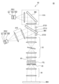
- FIG. 1 is a schematic diagram showing the configuration of an exposure apparatus according to an embodiment.
- FIG. 2 is a schematic diagram showing the configuration of the lighting unit.
- 3(A) is a front view of the first and second light source arrays
- FIG. 3(B) is a sectional view taken along the line AA in FIG. 3(A).
- FIG. 4 is a rear view of the board.
- FIG. 5 is a perspective view showing a heat sink and a first light source array.
- FIG. 6 is a perspective view showing the ⁇ Z1 side surface of the heat sink.
- FIG. 7(A) is a front view showing the heat sink and the first light source array
- FIG. 7(B) is a sectional view taken along the line AA in FIG. 7(A).
- FIG. 7(A) is a front view showing the heat sink and the first light source array
- FIG. 7(B) is a sectional view taken along the line AA in FIG. 7(A).
- FIG. 8 is a diagram for explaining the first and second enlarging optical systems.
- 9(A) is a front view showing a heat sink and a light source array according to a comparative example
- FIG. 9(B) is a sectional view taken along the line AA in FIG. 9(A).
- FIG. 10 is a diagram showing the measurement results of the surface temperature of the substrate.
- FIG. 11 is a sectional view for explaining a modification.
- FIG. 1 is a diagram schematically showing the configuration of an exposure apparatus 10 according to an embodiment.
- the exposure apparatus 10 drives the mask MSK and the glass substrate (hereinafter referred to as "plate") P in the same direction and at the same speed relative to the projection optical system PL, thereby transferring the pattern formed on the mask MSK to the plate P.
- This is a scanning stepper (scanner) that transfers images onto the image.
- the plate P is a rectangular glass substrate used, for example, in a liquid crystal display device (flat panel display), and has at least one side length or diagonal length of 500 mm or more.
- the direction in which the mask MSK and plate P are driven during scanning exposure is the X-axis direction
- the direction in the horizontal plane perpendicular to this is the Y-axis direction, which is perpendicular to the X-axis and the Y-axis.
- the direction of rotation is defined as the Z-axis direction
- the directions of rotation (tilt) around the X-axis, Y-axis, and Z-axis are defined as ⁇ x, ⁇ y, and ⁇ z directions, respectively.
- the exposure apparatus 10 includes an illumination system IOP, a mask stage MST holding a mask MSK, a projection optical system PL, a body 70 supporting these, a substrate stage PST holding a plate P, a control system for these, and the like.
- the control system centrally controls each component of the exposure apparatus 10.
- the body 70 includes a base (vibration isolator) 71, columns 72A, 72B, an optical surface plate 73, a support 74, and a slide guide 75.
- the base (vibration isolation table) 71 is placed on the floor F, isolates vibrations from the floor F, and supports the columns 72A, 72B, etc.
- Columns 72A and 72B each have a frame shape, and column 72A is arranged inside column 72B.
- the optical surface plate 73 has a flat plate shape and is fixed to the ceiling of the column 72A.
- the support body 74 is supported on the ceiling of the column 72B via a slide guide 75.
- Slide guide 75 includes an air ball lifter and a positioning mechanism, and positions support body 74 (that is, mask stage MST, which will be described later) at an appropriate position in the X-axis direction with respect to optical surface plate 73.
- the illumination system IOP is arranged above the body 70.
- the illumination system IOP irradiates the mask MSK with illumination light IL.
- the detailed configuration of the illumination system IOP will be described later.
- Mask stage MST is supported by support body 74.
- a mask MSK having a pattern surface (lower surface in FIG. 1) on which a circuit pattern is formed is fixed to the mask stage MST by, for example, vacuum suction (or electrostatic suction).
- Mask stage MST is driven with a predetermined stroke in the scanning direction (X-axis direction) by a drive system including, for example, a linear motor, and is also slightly driven in the non-scanning direction (Y-axis direction and ⁇ z direction).
- Positional information (including rotational information in the ⁇ z direction) of mask stage MST in the XY plane is measured by an interferometer system.
- the interferometer system irradiates a length measurement beam onto a movable mirror (or mirror-finished reflective surface (not shown)) provided at the end of mask stage MST, and receives reflected light from the movable mirror. Measure the position of mask stage MST.
- the measurement results are supplied to a control device (not shown), and the control device drives mask stage MST via a drive system according to the measurement results of the interferometer system.
- Projection optical system PL is supported by optical surface plate 73 below mask stage MST (-Z side).
- the projection optical system PL is configured similarly to the projection optical system disclosed in, for example, U.S. Pat. 7), and forms a rectangular image field whose longitudinal direction is the Y-axis direction.
- four projection optical units 100 are arranged at predetermined intervals in the Y-axis direction, and the remaining three projection optical units 100 are spaced apart from the four projection optical units 100 on the +X side and at predetermined intervals in the Y-axis direction. It is located in As each of the plurality of projection optical units 100, for example, one that forms an erect normal image with a double-sided telecentric, equal-magnification system is used.
- the plurality of projection areas of the projection optical units 100 arranged in a staggered manner are collectively referred to as an exposure area.
- the illumination light IL When the illumination region on the mask MSK is illuminated by the illumination light IL from the illumination system IOP, the illumination light IL that has passed through the mask MSK illuminates the circuit pattern of the mask MSK in the illumination region through the projection optical system PL.
- a projected image (partially erected image) is formed in an irradiation area (exposure area (conjugate to the illumination area)) on plate P arranged on the image plane side of projection optical system PL.
- the surface of the plate P is coated with a resist (sensitizer).
- Mask stage MST and substrate stage PST are driven synchronously, that is, mask MSK is driven in the scanning direction (X-axis direction) with respect to the illumination area (illumination light IL), and plate P is moved into the exposure area (illumination light IL). On the other hand, by driving in the same scanning direction, the plate P is exposed and the pattern of the mask MSK is transferred onto the plate P.
- the substrate stage PST is arranged on a base (vibration isolation table) 71 below (-Z side) the projection optical system PL.
- a plate P is held on substrate stage PST via a substrate holder (not shown).
- Position information in the XY plane of substrate stage PST (including rotation information (yawing amount (rotation amount ⁇ z in the ⁇ z direction), pitching amount (rotation amount ⁇ x in the ⁇ x direction), rolling amount (rotation amount ⁇ y in the ⁇ y direction)) is measured by an interferometer system.
- the interferometer system irradiates a length measurement beam from an optical surface plate 73 onto a movable mirror (or a mirror-finished reflective surface (not shown)) provided at the end of the substrate stage PST, and collects the reflected light from the movable mirror. By receiving light, the position of substrate stage PST is measured.
- the measurement results are supplied to a control device (not shown), and the control device drives substrate stage PST according to the measurement results of the interferometer system.
- the exposure apparatus 10 performs alignment measurement (eg, EGA, etc.) prior to exposure, and uses the results to expose the plate P according to the following procedure.
- mask stage MST and substrate stage PST are synchronously driven in the X-axis direction.
- the control device moves (steps) substrate stage PST to a position corresponding to the second shot area.
- scanning exposure is performed for the second shot area.
- the control device transfers the pattern of the mask MSK to all shot areas on the plate P by repeating stepping between shot areas of the plate P and scanning exposure for the shot areas.
- the illumination system IOP includes a plurality of illumination units 90 corresponding to each of the plurality of projection optical units 100 included in the projection optical system PL.
- FIG. 2 is a diagram schematically showing the configuration of the lighting unit 90.
- the illumination unit 90 includes a first light source unit OPU1, a second light source unit OPU2, and an illumination optical system 80.
- the first light source unit OPU1 includes a heat sink 40, a first light source array 20A, and a first enlarging optical system 30A
- the second light source unit OPU2 includes a heat sink 40, a second light source array 20B, and a second enlarging optical system. system 30B.
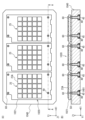
- FIG. 3(A) is a front view schematically showing the configuration of the first light source array 20A and the second light source array 20B
- FIG. 3(B) is a sectional view taken along the line AA in FIG. 3(A). be.
- FIG. 3(B) hatching of LED chips 23A and 23B, which will be described later, is omitted.
- the first light source array 20A includes a substrate 21A and a plurality of (5 ⁇ 5 in FIG. 3A) LEDs (Light Emitting Diodes) two-dimensionally arranged on the substrate 21A.
- a chip 23A is provided. The number of LED chips 23A may be changed as necessary.
- the substrate 21A has a first surface 21a and a second surface 21b facing each other, and LED chips 23A are arranged on the first surface 21a.
- the LED chips 23A are arranged at a pitch P1, and the pitch P1 is the distance between the centers of adjacent LED chips 23A.
- Each of the plurality of LED chips 23A has a light emitting section 231A, and the peak wavelength of light emitted from the light emitting section 231A is within the range of 380 to 390 nm. That is, the light emitting section 231A is an ultraviolet LED (UV LED). More preferably, the peak wavelength of the light emitted from the light emitting section 231A is 385 nm.
- the light emitting surface of the light emitting section 231A is square, and the length of one side thereof is a1.
- the two directions in which the LED chips 23A are arranged are referred to as the X1 direction and the Y1 direction.
- the X1 direction and the Y1 direction are orthogonal. Further, the direction perpendicular to the X1 direction and the Y1 direction is defined as the Z1 direction.
- the Z1 direction is approximately parallel to the optical axis of light emitted by the light emitting section 231A.
- the second light source array 20B includes a substrate 21B and a plurality of (5 ⁇ 5 in FIG. 3A) LED chips 23B two-dimensionally arranged on the substrate 21B.
- the number of LED chips 23B may be changed as necessary.
- the substrate 21B also has a first surface 21a and a second surface 21b facing each other, and LED chips 23B are arranged on the first surface 21a.
- the LED chips 23B are arranged at a pitch P2, and the pitch P2 is the distance between the centers of adjacent LED chips 23B.
- the arrangement pitch P1 of the LED chips 23A and the arrangement pitch P2 of the LED chips 23B may be the same or different.
- Each of the plurality of LED chips 23B has a light emitting section 231B, and the peak wavelength of light emitted from the light emitting section 231B is within the range of 360 to 370 nm. That is, the light emitting section 231B is a UV LED. More preferably, the peak wavelength of the light emitted from the light emitting section 231B is 365 nm.
- the light emitting surface of the light emitting section 231B is square, and the length of one side thereof is a2. The length a2 of one side of the light emitting surface of the light emitting section 231B may be the same as or different from the length a1 of one side of the light emitting surface of the light emitting section 231A.
- FIG. 4 is a rear view of the substrates 21A and 21B.
- the substrates 21A and 21B are metal substrates with a thickness of 5 mm or less.
- the substrates 21A and 21B are preferably made of a material with high thermal conductivity, and may be, for example, a copper substrate.
- on the second surface 21b of the substrates 21A, 21B opposite to the first surface 21a in a range where a plurality of LED chips 23A, 23B are arranged in plan view.
- a plurality of recesses 211 (3 ⁇ 3 in FIG. 4) are formed in the opposing portion AR1. In this embodiment, the plurality of recesses 211 are provided at equal intervals in each of the X1 direction and the Y1 direction.
- the recess 211 does not penetrate the substrates 21A and 21B.
- the recess 211 is a screw hole, and the boards 21A and 21B can be fixed to the heat sink 40 by engaging the bolt 61 in the recess 211, which will be described in detail later.
- FIG. 5 is a perspective view showing the heat sink 40 and the first light source array 20A
- FIG. 6 is a perspective view showing the -Z1 side surface of the heat sink 40
- FIG. 7(A) is a front view showing the heat sink 40 and the first light source array 20A
- FIG. 7(B) is a sectional view taken along the line AA in FIG. 7(A). Since the relationship between the second light source array 20B and the heat sink 40 is the same as the relationship between the first light source array 20A and the heat sink 40, the heat sink 40 and the first light source array 20A will be described below.
- FIG. 5 illustrates, as an example, a case where the first light source array 20A includes 10 ⁇ 14 LED chips 23A. Moreover, in FIG. 7(B), hatching of the LED chip 23A is omitted.
- first light source arrays 20A are arranged on the heat sink 40.
- the number of first light source arrays 20A arranged on the heat sink 40 is not limited to three, and may be two or less or four or more. That is, it is sufficient that at least one first light source array 20A is disposed on the heat sink 40.
- the heat sink 40 has a flow path 402 through which the refrigerant passes, a supply port 41 that supplies the refrigerant to the flow path 402, and an exhaust port 42 that discharges the refrigerant that has passed through the flow path 402. and cools the LED chips 23A included in the first light source array 20A.
- the refrigerant may be a liquid or a gas, but preferably water.
- the brightness of light from the light emitting section 231A included in the LED chip 23A decreases as the temperature of the LED chip 23A increases. In other words, the luminous efficiency of the LED chip 23A decreases as the temperature increases.
- the heat sink 40 has a through hole 401 that penetrates the heat sink 40, as shown in FIGS. 6 and 7(B).
- the through hole 401 is a stepped through hole whose diameter changes in two steps.
- a flow path 402 inside the heat sink 40 is formed in a portion where the through hole 401 is not formed.
- the through hole 401 is provided at a position corresponding to the recess 211 provided in the second surface 21b of the substrate 21A included in the first light source array 20A.
- a heat conductive member 50 such as Thermal Interface Material (TIM) is provided between the substrate 21A and the heat sink 40.
- TIM Thermal Interface Material
- a heat conductive sheet is used as the heat conductive member 50.
- the thermally conductive member 50 may be thermally conductive grease or the like.
- the thermally conductive member 50 is provided so as to be in contact with a portion AR1 of the second surface 21b of the substrate 21A that corresponds to at least the range where the LED chips 23A are arranged. Thereby, small gaps and unevenness between the substrate 21A and the heat sink 40 can be filled, and the LED chip 23A can be efficiently cooled by the heat sink 40.
- the heat sink 40 and the substrate 21A are fixed by bolts 61 that pass through the through holes 401 and engage (fit) into the recesses 211.
- the bolt 61 passes through the heat conductive member 50.
- the length of the bolt 61 is set to such a length that it passes through the heat conduction member 50 and allows the heat sink 40 and the heat conduction member 50 and the substrate 21A and the heat conduction member 50 to come into close contact with each other. Thereby, the heat sink 40 can cool the LED chip 23A more efficiently.
- the heat conductive member 50 is provided corresponding to each first light source array 20A, but for example, one sheet-like heat conductive member 50 is provided for three first light source arrays 20A. It may be provided.
- FIG. 8 is a diagram for explaining the first enlarging optical system 30A and the second enlarging optical system 30B that are included in the first light source unit OPU1 and the second light source unit OPU2, respectively.
- the first enlarging optical system 30A is an enlarging optical system for forming an enlarged image of the light emitting portion 231A of each LED chip 23A on a predetermined plane PP.
- the first magnifying optical system 30A includes a plurality of lens sections 31A arranged to correspond to the arrangement of the LED chips 23A.
- Each of the lens sections 31A is a double-sided telecentric optical system that enlarges and projects the light emitting section 231A at a magnification M1 equal to or greater than (array pitch P1 of LED chips 23B)/(length a1 of one side of the light emitting surface of the light emitting section 231A).
- M1 magnification
- FIG. 8 for clarity of the drawing, only four LED chips 23A (23B) lined up in a row along the Y1 direction are shown.
- the second enlarging optical system 30B is an enlarging optical system for forming an enlarged image of the light emitting portion 231B of each LED chip 23B on a predetermined plane PP.
- the second magnifying optical system 30B includes a plurality of lens sections 31B arranged to correspond to the arrangement of the LED chips 23B.
- Each lens section 31B is a double-sided telecentric optical system that enlarges and projects the light emitting section 231B at a magnification M2 equal to or greater than (array pitch P2 of the LED chips 23A)/(length a2 of one side of the light emitting surface of the light emitting section 231B). .
- each of the lens sections 31A and 31B includes four plano-convex lenses, but the invention is not limited to this.
- the lens sections 31A and 31B include two biconvex lenses. Alternatively, it may include three biconvex lenses.
- the lens portions 31A and 31B may include, for example, a plano-convex lens and a biconvex lens.
- the illumination optical system 80 includes a first condensing optical system (first optical system) 81A that includes a first dichroic mirror DM1, and a second condensing optical system (second optical system). (optical system) 81B, a second dichroic mirror DM2, an imaging optical system 83, a fly's eye lens FEL, and a condenser optical system 84.
- the first condensing optical system 81A forms a pupil of an enlarged image of the light emitting section 231A formed by the first enlarging optical system 30A. That is, the rear focal position of the first condensing optical system 81A is the position of the pupil.
- the first condensing optical system 81A includes a first dichroic mirror DM1 in the middle of the optical path, and reflects at least a portion of the light having a peak wavelength of 385 nm. As a result, the light beam enters the second dichroic mirror DM2.
- the first condensing optical system 81A may be configured without the first dichroic mirror DM1, and in that case, the arrangement of the first light source unit OPU1 and each lens of the first condensing optical system 81A may be changed. The arrangement may be appropriately adjusted so that the light beam is incident on the second dichroic mirror DM2. Further, the first condensing optical system 81A may be composed of one lens, or may be composed of a lens group including a plurality of lenses.
- the second condensing optical system 81B forms a pupil of an enlarged image of the light emitting section 231B formed by the second enlarging optical system 30B. That is, the rear focal position of the second condensing optical system 81B is the position of the pupil.
- the second condensing optical system 81B may be composed of one lens, or may be composed of a lens group including a plurality of lenses.
- the second dichroic mirror DM2 transmits at least part of the light with a peak wavelength of 385 nm and reflects at least part of the light with a peak wavelength of 365 nm. Thereby, a composite image is formed in which the pupil image formed by the first condensing optical system 81A and the pupil image formed by the second condensing optical system 81B are superimposed.
- the second dichroic mirror DM2 superimposes the pupil image formed by the first condensing optical system 81A and the pupil image formed by the second condensing optical system 81B to create a composite image. form. That is, the second dichroic mirror DM2 is arranged at a position that is the rear focal position of the first condensing optical system 81A and the rear focal position of the second condensing optical system 81B. Thereby, the second dichroic mirror DM2 is illuminated by Koehler illumination with the light emitted from the first light source unit OPU1 and the light emitted from the second light source unit OPU2.
- the first condensing optical system 81A and the second condensing optical system 81B respectively attach the image of the first light source unit OPU1 and the second condensing optical system to the second dichroic mirror DM2. It may be configured to perform critical illumination to form an image of the light source unit OPU2.
- the illumination unit 90 includes a detector DT10 for monitoring light with a peak wavelength of 385 nm, a detector DT20 for monitoring light with a peak wavelength of 365 nm, and a detector DT20 for monitoring light with a peak wavelength of 385 nm and light with a peak wavelength of 365 nm.
- a detector DT30 is provided for the detection.
- the detector DT10 detects the illuminance of the light with a peak wavelength of 385 nm reflected by the first dichroic mirror DM1.
- the detector DT20 detects the illuminance of the light having a peak wavelength of 365 nm reflected by the second dichroic mirror DM2.
- the detector DT30 detects the illuminance of the 385 nm light unintentionally reflected by the second dichroic mirror DM2 and the illuminance of the 365 nm light unintentionally transmitted by the second dichroic mirror DM2.
- the detection results of the detectors DT10 to DT30 are output to a control device (not shown), and the control device outputs the LED chips 23A of the first light source unit OPU1 and the second light source unit OPU2, respectively, based on the detection results of the detectors DT10 to DT30. and controls the value of the current supplied to 23B.
- the imaging optical system 83 is a double-sided telecentric optical system that projects the composite image synthesized by the second dichroic mirror DM2 at the same magnification onto the incident end of the fly's eye lens FEL. Note that the imaging optical system 83 may reduce and project the composite image synthesized by the second dichroic mirror DM2 onto the incident end of the fly's eye lens FEL.
- the fly's eye lens FEL is constructed by densely arranging a large number of lens elements each having, for example, positive refractive power, vertically and horizontally so that their optical axes are parallel to the reference optical axis AX.
- Each lens element constituting the fly's eye lens FEL has a rectangular cross section similar to the shape of the illumination field to be formed on the mask MSK (and thus the shape of the exposure area to be formed on the plate P).
- the light beam incident on the fly's eye lens FEL is wavefront-divided by a large number of lens elements, and one light source image is formed at or near the rear focal plane (output surface) of each lens element. That is, a substantial surface light source, ie, a secondary light source, consisting of a large number of light source images is formed at or near the rear focal plane (output surface) of the fly's eye lens FEL.
- a light beam from a secondary light source formed at or near the rear focal plane (output surface) of the fly's eye lens FEL enters an aperture stop 85 arranged near it.
- the rear focal plane (output surface) of the fly's eye lens FEL and the first light source array 20A and the second light source array 20B are optically conjugate.
- the aperture stop 85 is arranged at a position that is optically approximately conjugate with the entrance pupil plane of the projection optical system PL, and has a variable aperture for defining the range that contributes to the illumination of the secondary light source.
- the aperture stop 85 changes the aperture diameter of the variable aperture to determine the ⁇ value (the aperture of the secondary light source image on the pupil plane of the projection optical system relative to the aperture diameter of the pupil plane of the projection optical system), which determines the illumination condition. ratio) to the desired value.
- the light from the secondary light source passes through the aperture diaphragm 85 and, after being condensed by the condenser optical system 84, illuminates the mask MSK in which a predetermined pattern is formed in a superimposed manner.
- the wavelengths of the light emitted by the first light source unit OPU1 and the second light source unit OPU2 are not limited to those described above, and the first light source unit OPU1 and the second light source unit OPU2 may be The light source unit OPU1 and the second light source unit OPU2 may be configured.
- the first light source unit OPU1 may emit light with a peak wavelength of 405 nm
- the second light source unit OPU2 may emit light with a peak wavelength of 385 nm.
- the first light source unit OPU1 may emit light with a peak wavelength of 395 nm
- the second light source unit OPU2 may emit light with a peak wavelength of 385 nm.
- the combination of the wavelength of the light emitted from the first light source unit OPU1 and the wavelength of the light emitted from the second light source unit OPU2 is not limited to these examples. Note that if the combination of the wavelength of the light emitted by the first light source unit OPU1 and the wavelength of the light emitted by the second light source unit OPU2 is a combination other than that of the first embodiment, dichroic dichroic may be used as appropriate depending on the wavelength used. It is preferable to change the material of the mirror.
- the temperature of the substrate was determined when the heat sink and the substrate were fixed by the method according to the embodiment and when the heat sink and the substrate were fixed by the method according to the comparative example.
- the number of LED chips arranged in the light source array was 5 ⁇ 5.
- FIG. 9(A) is a front view showing a heat sink 1040 and a light source array 1020 according to a comparative example
- FIG. 9(B) is a sectional view taken along the line AA in FIG. 9(A).
- Each light source array 1020 includes a substrate 1021 and a plurality of LED chips 23A.
- the number of LED chips 23A provided on the substrate 1021 and the arrangement pitch are the same as those of the first light source array 20A.
- the heat sink 1040 according to the comparative example includes a through hole 1401 and a fixing block 45.
- Fixed block 45 is fixed to heat sink 1040 with bolts 46. Further, a screw hole is formed at the end of the fixed block 45 on the +Z1 side.
- Through holes are provided in the substrate 1021 at four locations outside the area where the plurality of LED chips 23A are arranged.
- the board 1021 is fixed to the heat sink 1040 by inserting the bolt 60 into the through hole from the +Z1 side and engaging the screw hole formed at the end of the fixing block 45 on the +Z1 side.
- the other configurations are the same as those in the embodiment, so detailed description will be omitted.
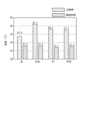
- FIG. 10 is a diagram showing the measurement results.
- the horizontal axis in FIG. 10 indicates each board, and the "left” is the board placed on the -Y1 side, the “center” is the board placed in the center, and the “right” is the board placed on the +Y1 side. "Average” indicates the average value for all substrates.
- the vertical axis in FIG. 10 indicates the temperature determined from the measurement value of the thermistor 25.
- the surface temperature of the substrate was lower than that using the method according to the comparative example. It was done. That is, it was confirmed that the fixing method according to the embodiment has a higher cooling effect on the LED chip 23A than the fixing method according to the comparative example. This is considered to be due to the following reasons.
- the board 1021 is fixed to the heat sink 1040 at four locations outside the range where the plurality of LED chips 23A are arranged. , the adhesion between the heat conductive member 50, the substrate 1021, and the heat sink 1040 becomes insufficient.
- the fixing method according to the embodiment since the substrate 21A can be fixed to the heat sink 40 at nine locations within the range where the LED chips 23A are arranged, the warping of the board 21A in the range where the LED chips 23A are arranged can be avoided. Deflection can be suppressed, and the adhesion between the heat conductive member 50, the substrate 21A, and the heat sink 40 can be improved. As a result, it is thought that the fixing method according to the embodiment has a higher cooling effect on the LED chip 23A than the fixing method according to the comparative example.
- the comparison can be made. It has been confirmed that the LED 23A can be cooled more efficiently than when the substrate 1021 and the heat sink 1040 are fixed by providing a mechanism for fixing the substrate 1021 and the heat sink 1040 outside the range where the LED chips 23A are arranged as in the example. Ta.
- the first light source unit OPU1 includes a substrate 21A having a first surface 21a and a second surface 21b facing each other, and
- the device includes LED chips 23A arranged two-dimensionally, a heat sink 40, and a heat conductive member 50 provided between the substrate 21A and the heat sink 40.
- the substrate 21A has a plurality of recesses 211 in a portion AR1 of the second surface 21b that faces the range where the LED chips 23A are arranged in a plan view
- the heat sink 40 has a through hole 401, which is connected to the substrate 21A.
- the heat sink 40 is fixed to the heat sink 40 with a bolt 61 that passes through the through hole 401 and fits into the recess 211 .
- the substrate 21A and the heat sink 40 are fixed outside the area where the LED chips 23A are arranged, warpage and deflection of the substrate 21A in the area where the LED chips 23A are arranged can be suppressed. Therefore, the adhesion between the heat conductive member 50, the substrate 21A, and the heat sink 40 can be improved. Therefore, the LED chip 23A can be efficiently cooled. Thereby, it is possible to suppress a decrease in the brightness of the light emitted from the light emitting section 231A due to a rise in the temperature of the LED chip 23A.
- the recess 211 is a screw hole. Therefore, the board 21A and the heat sink 40 can be easily fixed using the bolts 61.
- a plurality of recesses 211 are formed in the portion AR1 facing the range in which the LED chips 23A are arranged, and a plurality of through holes 401 are formed corresponding to the plurality of recesses 211.
- the board 21A and the heat sink 40 can be fixed at multiple locations, so the board 21A and the heat conductive member 50 and the heat conductive member 50 and the heat sink 40 can be brought into close contact with each other, and the LED chip 23A can be fixed more efficiently. Can be cooled.
- the plurality of recesses 211 and through holes 401 are formed at equal intervals. This makes it possible to equalize the force acting on the board 21A from the bolts 61, so that distortion, deflection, etc. of the board 21A can be suppressed.
- the recess 211 does not penetrate the substrate 21A. This can prevent the bolt 61 from coming into contact with the LED chip 23A.
- the substrate 21A is a metal substrate. Therefore, the recess 211 can be easily formed.
- the heat conduction member 50 was provided between the heat sink 40 and the substrate 21A, but the heat conduction member 50 may be omitted. That is, the heat sink 40 and the substrate 21A may be fixed with the bolts 61 so that the heat sink 40 and the substrate 21A are in direct contact with each other. Even in this case, the LED chip 23A can be cooled, and the brightness of the light emitted by the light emitting part 231A of the LED chip 23A can be prevented from decreasing due to a rise in the temperature of the LED chip 23A.
- the recess 211 is a screw hole, but it is not limited to this.
- the recess 211 may be a hole without a thread groove.
- a fixing member that fits into the recess 211 may be used, and the fixing member may be fixed to the substrate 21A by soldering or adhesive.
- a plurality of recesses 211 are provided, and at least one recess 211 is provided in a portion of the second surface 21b of the substrate 21A that corresponds to a portion where the LED chips 23A are arranged. It is sufficient if it is formed. Further, the number of recesses 211 is not limited to the above embodiment, and may be 8 or less, or 10 or more.
- the recesses 211 are provided at equal intervals in each of the X1 direction and the Y1 direction, but they may be provided at irregular intervals.
- the through hole 401 of the heat sink 40 may be formed at a position corresponding to the position of the recess 211.
- the heat sink 40 had the flow path 402 through which the refrigerant flows inside, but the heat sink 40 is not limited to this.
- the heat sink 40 may be, for example, a fin type heat sink.
- a control unit CTR for controlling the LED chips 23A may be arranged on the surface of the heat sink 40 opposite to the surface on which the substrates 21A are arranged.
- the control unit CTR can be cooled by the heat sink 40, there is no need to separately provide a mechanism for cooling the control unit CTR, and the configuration of the first light source unit OPU1 can be simplified.
- the illumination unit 90 includes the first light source unit OPU1, the second light source unit OPU2, and the illumination optical system 80 including the second dichroic mirror DM2. It is not limited.
- the lighting unit 90 may include only one of the first light source unit OPU1 and the second light source unit OPU2.
- the illumination optical system 80 can have any configuration as long as it can guide the light emitted from the first light source unit OPU1 or the second light source unit OPU2 to the mask MSK.
- Exposure device 20A First light source array 20B Second light source array 21A, 21B Substrate 21a First surface 21b Second surface 23A, 23B LED chip 30A First magnifying optical system 30B Second magnifying optical system 31A, 31B Lens section 40 Heat sink 50 Thermal conduction member 61 Bolt 211 Recesses 231A, 231B Light emitting section 401 Through hole 80 Illumination optical system 90 Illumination unit 100 Projection optical unit CTR Control section DM2 Second dichroic mirror MSK Mask OPU1 First light source unit OPU2 Second light source unit P Glass substrate
Landscapes
- Physics & Mathematics (AREA)
- General Physics & Mathematics (AREA)
- Health & Medical Sciences (AREA)
- Engineering & Computer Science (AREA)
- Environmental & Geological Engineering (AREA)
- Epidemiology (AREA)
- Public Health (AREA)
- Life Sciences & Earth Sciences (AREA)
- Atmospheric Sciences (AREA)
- Toxicology (AREA)
- Exposure And Positioning Against Photoresist Photosensitive Materials (AREA)
- Light Sources And Details Of Projection-Printing Devices (AREA)
- Fastening Of Light Sources Or Lamp Holders (AREA)
Priority Applications (5)
| Application Number | Priority Date | Filing Date | Title |
|---|---|---|---|
| JP2024541343A JPWO2024038537A1 (https=) | 2022-08-18 | 2022-08-18 | |
| PCT/JP2022/031212 WO2024038537A1 (ja) | 2022-08-18 | 2022-08-18 | 光源ユニット、照明ユニット、露光装置、及び露光方法 |
| CN202280099101.1A CN119790351A (zh) | 2022-08-18 | 2022-08-18 | 光源单元、照明单元、曝光装置、以及曝光方法 |
| KR1020257004339A KR20250036881A (ko) | 2022-08-18 | 2022-08-18 | 광원 유닛, 조명 유닛, 노광 장치, 및 노광 방법 |
| TW112127508A TWI855790B (zh) | 2022-08-18 | 2023-07-24 | 光源單元、照明單元、曝光裝置、及曝光方法 |
Applications Claiming Priority (1)
| Application Number | Priority Date | Filing Date | Title |
|---|---|---|---|
| PCT/JP2022/031212 WO2024038537A1 (ja) | 2022-08-18 | 2022-08-18 | 光源ユニット、照明ユニット、露光装置、及び露光方法 |
Publications (1)
| Publication Number | Publication Date |
|---|---|
| WO2024038537A1 true WO2024038537A1 (ja) | 2024-02-22 |
Family
ID=89941586
Family Applications (1)
| Application Number | Title | Priority Date | Filing Date |
|---|---|---|---|
| PCT/JP2022/031212 Ceased WO2024038537A1 (ja) | 2022-08-18 | 2022-08-18 | 光源ユニット、照明ユニット、露光装置、及び露光方法 |
Country Status (5)
| Country | Link |
|---|---|
| JP (1) | JPWO2024038537A1 (https=) |
| KR (1) | KR20250036881A (https=) |
| CN (1) | CN119790351A (https=) |
| TW (1) | TWI855790B (https=) |
| WO (1) | WO2024038537A1 (https=) |
Citations (4)
| Publication number | Priority date | Publication date | Assignee | Title |
|---|---|---|---|---|
| US6683421B1 (en) * | 2001-01-25 | 2004-01-27 | Exfo Photonic Solutions Inc. | Addressable semiconductor array light source for localized radiation delivery |
| WO2014061555A1 (ja) * | 2012-10-19 | 2014-04-24 | シャープ株式会社 | 発光装置および発光装置のヒートシンクへの取付構造 |
| JP2016041959A (ja) * | 2014-08-18 | 2016-03-31 | カシオ計算機株式会社 | 締結構造及びこの締結構造を備える投影装置、締結方法 |
| JP2017048263A (ja) * | 2015-08-31 | 2017-03-09 | 公立大学法人大阪府立大学 | 光硬化性樹脂組成物の硬化物の製造方法および光照射装置 |
Family Cites Families (6)
| Publication number | Priority date | Publication date | Assignee | Title |
|---|---|---|---|---|
| JP4587170B2 (ja) | 2005-01-20 | 2010-11-24 | キヤノン株式会社 | 露光装置及びデバイスの製造方法 |
| KR102315472B1 (ko) * | 2017-03-31 | 2021-10-21 | 가부시키가이샤 니콘 | 물체 유지 장치, 처리 장치, 플랫 패널 디스플레이의 제조 방법, 디바이스 제조 방법, 및 물체 유지 방법 |
| WO2019064511A1 (ja) * | 2017-09-29 | 2019-04-04 | 株式会社ニコン | 電子ビーム装置及びデバイス製造方法 |
| WO2019064521A1 (ja) * | 2017-09-29 | 2019-04-04 | 株式会社ニコン | 電子ビーム装置及びデバイス製造方法 |
| WO2019064520A1 (ja) * | 2017-09-29 | 2019-04-04 | 株式会社ニコン | 電子ビーム装置及びデバイス製造方法 |
| WO2019064516A1 (ja) * | 2017-09-29 | 2019-04-04 | 株式会社ニコン | 電子ビーム装置及びデバイス製造方法 |
-
2022
- 2022-08-18 WO PCT/JP2022/031212 patent/WO2024038537A1/ja not_active Ceased
- 2022-08-18 CN CN202280099101.1A patent/CN119790351A/zh active Pending
- 2022-08-18 KR KR1020257004339A patent/KR20250036881A/ko active Pending
- 2022-08-18 JP JP2024541343A patent/JPWO2024038537A1/ja active Pending
-
2023
- 2023-07-24 TW TW112127508A patent/TWI855790B/zh active
Patent Citations (4)
| Publication number | Priority date | Publication date | Assignee | Title |
|---|---|---|---|---|
| US6683421B1 (en) * | 2001-01-25 | 2004-01-27 | Exfo Photonic Solutions Inc. | Addressable semiconductor array light source for localized radiation delivery |
| WO2014061555A1 (ja) * | 2012-10-19 | 2014-04-24 | シャープ株式会社 | 発光装置および発光装置のヒートシンクへの取付構造 |
| JP2016041959A (ja) * | 2014-08-18 | 2016-03-31 | カシオ計算機株式会社 | 締結構造及びこの締結構造を備える投影装置、締結方法 |
| JP2017048263A (ja) * | 2015-08-31 | 2017-03-09 | 公立大学法人大阪府立大学 | 光硬化性樹脂組成物の硬化物の製造方法および光照射装置 |
Also Published As
| Publication number | Publication date |
|---|---|
| TWI855790B (zh) | 2024-09-11 |
| KR20250036881A (ko) | 2025-03-14 |
| JPWO2024038537A1 (https=) | 2024-02-22 |
| TW202417999A (zh) | 2024-05-01 |
| CN119790351A (zh) | 2025-04-08 |
Similar Documents
| Publication | Publication Date | Title |
|---|---|---|
| CN101299134B (zh) | 光刻设备和方法 | |
| TW200941901A (en) | Planar motor and stage using the same | |
| WO2002054460A1 (fr) | Dispositif d'exposition | |
| JP4678493B2 (ja) | 光源ユニット、照明光学装置、露光装置、および露光方法 | |
| WO2024038537A1 (ja) | 光源ユニット、照明ユニット、露光装置、及び露光方法 | |
| US20240126176A1 (en) | Spatial light modulation unit and exposure apparatus | |
| TWI885424B (zh) | 照明單元、曝光裝置、及曝光方法 | |
| TWI915769B (zh) | 光源單元、照明單元、曝光裝置、以及曝光方法 | |
| TWI876438B (zh) | 光源單元、照明單元、曝光裝置、及曝光方法 | |
| TWI915658B (zh) | 光源單元、照明單元、曝光裝置、及曝光方法 | |
| WO2024209586A1 (ja) | 光源ユニット、照明ユニット、露光装置、及び露光方法 | |
| KR20250160466A (ko) | 구동 방법, 광원 유닛, 조명 유닛, 노광 장치, 및 노광 방법 | |
| WO2024038538A1 (ja) | 光源ユニット、照明ユニット、露光装置、及び露光方法 | |
| JP2007025085A (ja) | 露光装置、光学素子アレー及びマルチスポットビームジェネレータ、並びにデバイス製造方法 | |
| CN121934325A (zh) | 光源装置、曝光装置和物品的制造方法 | |
| WO2025079172A1 (ja) | 光源ユニット、照明ユニット、露光装置、及び露光方法 | |
| JP2026056837A (ja) | 光源装置、露光装置、及び物品の製造方法 | |
| KR20260060422A (ko) | 광원 유닛, 조명 유닛, 노광 장치, 및 노광 방법 | |
| WO2025013286A1 (ja) | 照明ユニット、露光装置、及び露光方法 | |
| KR20260061012A (ko) | 광원 장치, 노광 장치, 및 물품의 제조 방법 | |
| KR20250060918A (ko) | 합성 광학 소자, 조명 유닛, 노광 장치, 및 노광 방법 | |
| JP2007093646A (ja) | 直接描画装置 | |
| RAYS | KujaWski (PL) | |
| JP2014149391A (ja) | パターン形成装置及びパターン形成方法 |
Legal Events
| Date | Code | Title | Description |
|---|---|---|---|
| 121 | Ep: the epo has been informed by wipo that ep was designated in this application |
Ref document number: 22955711 Country of ref document: EP Kind code of ref document: A1 |
|
| WWE | Wipo information: entry into national phase |
Ref document number: 2024541343 Country of ref document: JP |
|
| ENP | Entry into the national phase |
Ref document number: 20257004339 Country of ref document: KR Kind code of ref document: A |
|
| WWE | Wipo information: entry into national phase |
Ref document number: 1020257004339 Country of ref document: KR |
|
| WWE | Wipo information: entry into national phase |
Ref document number: 202280099101.1 Country of ref document: CN |
|
| WWP | Wipo information: published in national office |
Ref document number: 1020257004339 Country of ref document: KR |
|
| NENP | Non-entry into the national phase |
Ref country code: DE |
|
| WWP | Wipo information: published in national office |
Ref document number: 202280099101.1 Country of ref document: CN |
|
| 122 | Ep: pct application non-entry in european phase |
Ref document number: 22955711 Country of ref document: EP Kind code of ref document: A1 |