WO2024033742A1 - シフトレジスタ - Google Patents
シフトレジスタ Download PDFInfo
- Publication number
- WO2024033742A1 WO2024033742A1 PCT/IB2023/057662 IB2023057662W WO2024033742A1 WO 2024033742 A1 WO2024033742 A1 WO 2024033742A1 IB 2023057662 W IB2023057662 W IB 2023057662W WO 2024033742 A1 WO2024033742 A1 WO 2024033742A1
- Authority
- WO
- WIPO (PCT)
- Prior art keywords
- transistor
- layer
- conductive layer
- pixel
- light
- Prior art date
- Legal status (The legal status is an assumption and is not a legal conclusion. Google has not performed a legal analysis and makes no representation as to the accuracy of the status listed.)
- Ceased
Links
Images







































Classifications
-
- G—PHYSICS
- G11—INFORMATION STORAGE
- G11C—STATIC STORES
- G11C19/00—Digital stores in which the information is moved stepwise, e.g. shift registers
- G11C19/28—Digital stores in which the information is moved stepwise, e.g. shift registers using semiconductor elements
-
- G—PHYSICS
- G09—EDUCATION; CRYPTOGRAPHY; DISPLAY; ADVERTISING; SEALS
- G09G—ARRANGEMENTS OR CIRCUITS FOR CONTROL OF INDICATING DEVICES USING STATIC MEANS TO PRESENT VARIABLE INFORMATION
- G09G3/00—Control arrangements or circuits, of interest only in connection with visual indicators other than cathode-ray tubes
- G09G3/20—Control arrangements or circuits, of interest only in connection with visual indicators other than cathode-ray tubes for presentation of an assembly of a number of characters, e.g. a page, by composing the assembly by combination of individual elements arranged in a matrix no fixed position being assigned to or needed to be assigned to the individual characters or partial characters
-
- G—PHYSICS
- G09—EDUCATION; CRYPTOGRAPHY; DISPLAY; ADVERTISING; SEALS
- G09G—ARRANGEMENTS OR CIRCUITS FOR CONTROL OF INDICATING DEVICES USING STATIC MEANS TO PRESENT VARIABLE INFORMATION
- G09G3/00—Control arrangements or circuits, of interest only in connection with visual indicators other than cathode-ray tubes
- G09G3/20—Control arrangements or circuits, of interest only in connection with visual indicators other than cathode-ray tubes for presentation of an assembly of a number of characters, e.g. a page, by composing the assembly by combination of individual elements arranged in a matrix no fixed position being assigned to or needed to be assigned to the individual characters or partial characters
- G09G3/22—Control arrangements or circuits, of interest only in connection with visual indicators other than cathode-ray tubes for presentation of an assembly of a number of characters, e.g. a page, by composing the assembly by combination of individual elements arranged in a matrix no fixed position being assigned to or needed to be assigned to the individual characters or partial characters using controlled light sources
- G09G3/30—Control arrangements or circuits, of interest only in connection with visual indicators other than cathode-ray tubes for presentation of an assembly of a number of characters, e.g. a page, by composing the assembly by combination of individual elements arranged in a matrix no fixed position being assigned to or needed to be assigned to the individual characters or partial characters using controlled light sources using electroluminescent panels
- G09G3/32—Control arrangements or circuits, of interest only in connection with visual indicators other than cathode-ray tubes for presentation of an assembly of a number of characters, e.g. a page, by composing the assembly by combination of individual elements arranged in a matrix no fixed position being assigned to or needed to be assigned to the individual characters or partial characters using controlled light sources using electroluminescent panels semiconductive, e.g. using light-emitting diodes [LED]
- G09G3/3208—Control arrangements or circuits, of interest only in connection with visual indicators other than cathode-ray tubes for presentation of an assembly of a number of characters, e.g. a page, by composing the assembly by combination of individual elements arranged in a matrix no fixed position being assigned to or needed to be assigned to the individual characters or partial characters using controlled light sources using electroluminescent panels semiconductive, e.g. using light-emitting diodes [LED] organic, e.g. using organic light-emitting diodes [OLED]
- G09G3/3266—Details of drivers for scan electrodes
-
- G—PHYSICS
- G09—EDUCATION; CRYPTOGRAPHY; DISPLAY; ADVERTISING; SEALS
- G09G—ARRANGEMENTS OR CIRCUITS FOR CONTROL OF INDICATING DEVICES USING STATIC MEANS TO PRESENT VARIABLE INFORMATION
- G09G3/00—Control arrangements or circuits, of interest only in connection with visual indicators other than cathode-ray tubes
- G09G3/20—Control arrangements or circuits, of interest only in connection with visual indicators other than cathode-ray tubes for presentation of an assembly of a number of characters, e.g. a page, by composing the assembly by combination of individual elements arranged in a matrix no fixed position being assigned to or needed to be assigned to the individual characters or partial characters
- G09G3/22—Control arrangements or circuits, of interest only in connection with visual indicators other than cathode-ray tubes for presentation of an assembly of a number of characters, e.g. a page, by composing the assembly by combination of individual elements arranged in a matrix no fixed position being assigned to or needed to be assigned to the individual characters or partial characters using controlled light sources
- G09G3/30—Control arrangements or circuits, of interest only in connection with visual indicators other than cathode-ray tubes for presentation of an assembly of a number of characters, e.g. a page, by composing the assembly by combination of individual elements arranged in a matrix no fixed position being assigned to or needed to be assigned to the individual characters or partial characters using controlled light sources using electroluminescent panels
- G09G3/32—Control arrangements or circuits, of interest only in connection with visual indicators other than cathode-ray tubes for presentation of an assembly of a number of characters, e.g. a page, by composing the assembly by combination of individual elements arranged in a matrix no fixed position being assigned to or needed to be assigned to the individual characters or partial characters using controlled light sources using electroluminescent panels semiconductive, e.g. using light-emitting diodes [LED]
- G09G3/3208—Control arrangements or circuits, of interest only in connection with visual indicators other than cathode-ray tubes for presentation of an assembly of a number of characters, e.g. a page, by composing the assembly by combination of individual elements arranged in a matrix no fixed position being assigned to or needed to be assigned to the individual characters or partial characters using controlled light sources using electroluminescent panels semiconductive, e.g. using light-emitting diodes [LED] organic, e.g. using organic light-emitting diodes [OLED]
- G09G3/3275—Details of drivers for data electrodes
-
- G—PHYSICS
- G09—EDUCATION; CRYPTOGRAPHY; DISPLAY; ADVERTISING; SEALS
- G09G—ARRANGEMENTS OR CIRCUITS FOR CONTROL OF INDICATING DEVICES USING STATIC MEANS TO PRESENT VARIABLE INFORMATION
- G09G3/00—Control arrangements or circuits, of interest only in connection with visual indicators other than cathode-ray tubes
- G09G3/20—Control arrangements or circuits, of interest only in connection with visual indicators other than cathode-ray tubes for presentation of an assembly of a number of characters, e.g. a page, by composing the assembly by combination of individual elements arranged in a matrix no fixed position being assigned to or needed to be assigned to the individual characters or partial characters
- G09G3/34—Control arrangements or circuits, of interest only in connection with visual indicators other than cathode-ray tubes for presentation of an assembly of a number of characters, e.g. a page, by composing the assembly by combination of individual elements arranged in a matrix no fixed position being assigned to or needed to be assigned to the individual characters or partial characters by control of light from an independent source
- G09G3/36—Control arrangements or circuits, of interest only in connection with visual indicators other than cathode-ray tubes for presentation of an assembly of a number of characters, e.g. a page, by composing the assembly by combination of individual elements arranged in a matrix no fixed position being assigned to or needed to be assigned to the individual characters or partial characters by control of light from an independent source using liquid crystals
- G09G3/3611—Control of matrices with row and column drivers
- G09G3/3674—Details of drivers for scan electrodes
- G09G3/3677—Details of drivers for scan electrodes suitable for active matrices only
-
- G—PHYSICS
- G09—EDUCATION; CRYPTOGRAPHY; DISPLAY; ADVERTISING; SEALS
- G09G—ARRANGEMENTS OR CIRCUITS FOR CONTROL OF INDICATING DEVICES USING STATIC MEANS TO PRESENT VARIABLE INFORMATION
- G09G3/00—Control arrangements or circuits, of interest only in connection with visual indicators other than cathode-ray tubes
- G09G3/20—Control arrangements or circuits, of interest only in connection with visual indicators other than cathode-ray tubes for presentation of an assembly of a number of characters, e.g. a page, by composing the assembly by combination of individual elements arranged in a matrix no fixed position being assigned to or needed to be assigned to the individual characters or partial characters
- G09G3/34—Control arrangements or circuits, of interest only in connection with visual indicators other than cathode-ray tubes for presentation of an assembly of a number of characters, e.g. a page, by composing the assembly by combination of individual elements arranged in a matrix no fixed position being assigned to or needed to be assigned to the individual characters or partial characters by control of light from an independent source
- G09G3/36—Control arrangements or circuits, of interest only in connection with visual indicators other than cathode-ray tubes for presentation of an assembly of a number of characters, e.g. a page, by composing the assembly by combination of individual elements arranged in a matrix no fixed position being assigned to or needed to be assigned to the individual characters or partial characters by control of light from an independent source using liquid crystals
- G09G3/3611—Control of matrices with row and column drivers
- G09G3/3685—Details of drivers for data electrodes
- G09G3/3688—Details of drivers for data electrodes suitable for active matrices only
-
- H—ELECTRICITY
- H10—SEMICONDUCTOR DEVICES; ELECTRIC SOLID-STATE DEVICES NOT OTHERWISE PROVIDED FOR
- H10D—INORGANIC ELECTRIC SEMICONDUCTOR DEVICES
- H10D30/00—Field-effect transistors [FET]
- H10D30/60—Insulated-gate field-effect transistors [IGFET]
- H10D30/67—Thin-film transistors [TFT]
-
- H—ELECTRICITY
- H10—SEMICONDUCTOR DEVICES; ELECTRIC SOLID-STATE DEVICES NOT OTHERWISE PROVIDED FOR
- H10D—INORGANIC ELECTRIC SEMICONDUCTOR DEVICES
- H10D30/00—Field-effect transistors [FET]
- H10D30/60—Insulated-gate field-effect transistors [IGFET]
- H10D30/67—Thin-film transistors [TFT]
- H10D30/6728—Vertical TFTs
-
- H—ELECTRICITY
- H10—SEMICONDUCTOR DEVICES; ELECTRIC SOLID-STATE DEVICES NOT OTHERWISE PROVIDED FOR
- H10D—INORGANIC ELECTRIC SEMICONDUCTOR DEVICES
- H10D30/00—Field-effect transistors [FET]
- H10D30/60—Insulated-gate field-effect transistors [IGFET]
- H10D30/67—Thin-film transistors [TFT]
- H10D30/6729—Thin-film transistors [TFT] characterised by the electrodes
- H10D30/673—Thin-film transistors [TFT] characterised by the electrodes characterised by the shapes, relative sizes or dispositions of the gate electrodes
- H10D30/6733—Multi-gate TFTs
- H10D30/6734—Multi-gate TFTs having gate electrodes arranged on both top and bottom sides of the channel, e.g. dual-gate TFTs
-
- H—ELECTRICITY
- H10—SEMICONDUCTOR DEVICES; ELECTRIC SOLID-STATE DEVICES NOT OTHERWISE PROVIDED FOR
- H10D—INORGANIC ELECTRIC SEMICONDUCTOR DEVICES
- H10D86/00—Integrated devices formed in or on insulating or conducting substrates, e.g. formed in silicon-on-insulator [SOI] substrates or on stainless steel or glass substrates
- H10D86/40—Integrated devices formed in or on insulating or conducting substrates, e.g. formed in silicon-on-insulator [SOI] substrates or on stainless steel or glass substrates characterised by multiple TFTs
-
- H—ELECTRICITY
- H10—SEMICONDUCTOR DEVICES; ELECTRIC SOLID-STATE DEVICES NOT OTHERWISE PROVIDED FOR
- H10D—INORGANIC ELECTRIC SEMICONDUCTOR DEVICES
- H10D86/00—Integrated devices formed in or on insulating or conducting substrates, e.g. formed in silicon-on-insulator [SOI] substrates or on stainless steel or glass substrates
- H10D86/40—Integrated devices formed in or on insulating or conducting substrates, e.g. formed in silicon-on-insulator [SOI] substrates or on stainless steel or glass substrates characterised by multiple TFTs
- H10D86/421—Integrated devices formed in or on insulating or conducting substrates, e.g. formed in silicon-on-insulator [SOI] substrates or on stainless steel or glass substrates characterised by multiple TFTs having a particular composition, shape or crystalline structure of the active layer
- H10D86/423—Integrated devices formed in or on insulating or conducting substrates, e.g. formed in silicon-on-insulator [SOI] substrates or on stainless steel or glass substrates characterised by multiple TFTs having a particular composition, shape or crystalline structure of the active layer comprising semiconductor materials not belonging to the Group IV, e.g. InGaZnO
-
- H—ELECTRICITY
- H10—SEMICONDUCTOR DEVICES; ELECTRIC SOLID-STATE DEVICES NOT OTHERWISE PROVIDED FOR
- H10D—INORGANIC ELECTRIC SEMICONDUCTOR DEVICES
- H10D86/00—Integrated devices formed in or on insulating or conducting substrates, e.g. formed in silicon-on-insulator [SOI] substrates or on stainless steel or glass substrates
- H10D86/40—Integrated devices formed in or on insulating or conducting substrates, e.g. formed in silicon-on-insulator [SOI] substrates or on stainless steel or glass substrates characterised by multiple TFTs
- H10D86/60—Integrated devices formed in or on insulating or conducting substrates, e.g. formed in silicon-on-insulator [SOI] substrates or on stainless steel or glass substrates characterised by multiple TFTs wherein the TFTs are in active matrices
-
- G—PHYSICS
- G09—EDUCATION; CRYPTOGRAPHY; DISPLAY; ADVERTISING; SEALS
- G09G—ARRANGEMENTS OR CIRCUITS FOR CONTROL OF INDICATING DEVICES USING STATIC MEANS TO PRESENT VARIABLE INFORMATION
- G09G2300/00—Aspects of the constitution of display devices
- G09G2300/04—Structural and physical details of display devices
- G09G2300/0421—Structural details of the set of electrodes
- G09G2300/0426—Layout of electrodes and connections
-
- G—PHYSICS
- G09—EDUCATION; CRYPTOGRAPHY; DISPLAY; ADVERTISING; SEALS
- G09G—ARRANGEMENTS OR CIRCUITS FOR CONTROL OF INDICATING DEVICES USING STATIC MEANS TO PRESENT VARIABLE INFORMATION
- G09G2310/00—Command of the display device
- G09G2310/02—Addressing, scanning or driving the display screen or processing steps related thereto
- G09G2310/0264—Details of driving circuits
- G09G2310/0286—Details of a shift registers arranged for use in a driving circuit
-
- H—ELECTRICITY
- H03—ELECTRONIC CIRCUITRY
- H03K—PULSE TECHNIQUE
- H03K19/00—Logic circuits, i.e. having at least two inputs acting on one output; Inverting circuits
- H03K19/02—Logic circuits, i.e. having at least two inputs acting on one output; Inverting circuits using specified components
- H03K19/08—Logic circuits, i.e. having at least two inputs acting on one output; Inverting circuits using specified components using semiconductor devices
- H03K19/094—Logic circuits, i.e. having at least two inputs acting on one output; Inverting circuits using specified components using semiconductor devices using field-effect transistors
Definitions
- One embodiment of the invention disclosed in this specification and the like relates to a product, a method, or a manufacturing method.
- one embodiment of the invention disclosed in this specification and the like relates to a process, a machine, a manufacture, or a composition of matter.
- One aspect of the invention is not limited to the technical fields described above.
- Technical fields of one embodiment of the invention disclosed in this specification etc. include semiconductor devices, display devices, light emitting devices, power storage devices, storage devices, electronic devices, lighting devices, input devices (e.g. touch sensors), and input/output devices.
- Examples include touch panels (for example, touch panels), their driving methods, or their manufacturing methods.
- a semiconductor device is a device that utilizes semiconductor characteristics, and refers to a circuit including a semiconductor element (transistor, diode, photodiode, etc.), a device having the same circuit, and the like. It also refers to any device that can function by utilizing the characteristics of semiconductors. For example, an integrated circuit, a chip including an integrated circuit, and an electronic component containing a chip in a package are examples of semiconductor devices. Further, storage devices, display devices, light emitting devices, lighting devices, electronic devices, and the like may themselves be semiconductor devices, and each may include a semiconductor device.
- Oxide semiconductors using metal oxides are attracting attention as semiconductor materials applicable to transistors.
- a plurality of oxide semiconductor layers are stacked, and among the plurality of oxide semiconductor layers, an oxide semiconductor layer serving as a channel contains indium and gallium, and the proportion of indium is set to a proportion of gallium.
- a semiconductor device has been disclosed in which field effect mobility (sometimes simply referred to as mobility or ⁇ FE) is increased by increasing the field effect mobility.
- An object of one embodiment of the present invention is to provide a semiconductor device that occupies a small area.
- one of the challenges is to provide a semiconductor device with low power consumption.
- one of the challenges is to provide a semiconductor device with good reliability.
- one of the challenges is to provide a new semiconductor device.
- One embodiment of the present invention includes a plurality of signal output circuits, at least one of the plurality of signal output circuits includes a first transistor, and at least one of the plurality of signal output circuits transmits a first signal to a first transistor.
- a shift register having a function of outputting through a transistor, the shift register having a first conductive layer having a region functioning as either a source electrode or a drain electrode of the first transistor, and a region disposed on the first conductive layer.
- a first insulating layer a first insulating layer
- a second conductive layer having a region functioning as the other of the source electrode or the drain electrode of the first transistor and disposed on the first insulating layer
- a third conductive layer having a semiconductor layer, a region functioning as a gate electrode of the first transistor, and a region functioning as a gate insulating film of the first transistor; a second insulating layer having a region sandwiched by one opening, the first signal being a shift register input to one of the source electrode or the drain electrode of the first transistor.
- the third conductive layer has a region overlapping with the first conductive layer in the first opening and a region overlapping with the second conductive layer on the first insulating layer.
- At least one of the plurality of signal output circuits may include a second transistor.
- a second transistor For example, a fourth conductive layer having a region functioning as one of a source electrode or a drain electrode of the second transistor, a first insulating layer having a region disposed on the fourth conductive layer, and a source electrode or a drain electrode of the first transistor; a fifth conductive layer having a region functioning as the other drain electrode and disposed on the first insulating layer; and a fourth conductive layer penetrating the first insulating layer and the fifth conductive layer; an overlapping second opening, a second semiconductor layer having a region in contact with the first insulating layer, a region in contact with the fourth conductive layer, and a region in contact with the fifth conductive layer, and a gate electrode of the second transistor.
- a sixth conductive layer having a region functioning as a gate insulating layer of the second transistor and having a region disposed on the second insulating layer; and a region functioning as a gate insulating film of the second transistor; and a second insulating layer having a region sandwiched by the second opening.
- the fourth conductive layer and the third conductive layer are electrically connected to each other.
- the height of the top surface of the fourth conductive layer may be different from the height of the bottom surface of the sixth conductive layer.
- the first semiconductor layer contains an oxide semiconductor.
- the second semiconductor layer contains an oxide semiconductor.
- a semiconductor device that occupies a small area can be provided.
- a semiconductor device with low power consumption can be provided.
- a semiconductor device with good reliability can be provided.
- a new semiconductor device can be provided.
- FIG. 1A is a diagram showing an example of a shift register.
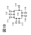
- FIG. 1B and FIG. 1C are diagrams showing an example of a signal output circuit.
- FIG. 2 is a diagram showing an example of a signal output circuit.
- FIG. 3 is a diagram showing an example of a signal output circuit.
- FIG. 4 is a diagram showing an example of a signal output circuit.
- FIG. 5 is a diagram showing an example of a signal output circuit.
- FIG. 6 is a diagram showing an example of a signal output circuit.
- FIG. 7 is a diagram showing an example of a signal output circuit.
- FIG. 8 is a diagram showing an example of a signal output circuit.
- FIG. 9 is a diagram showing an example of a signal output circuit.
- FIG. 10 is a diagram showing an example of a signal output circuit.
- FIG. 11A is a plan view of the transistor.
- FIG. 11B is a cross-sectional view of the transistor.
- FIG. 11C is a perspective view of the transistor.
- FIG. 11D is an equivalent circuit diagram of a transistor.
- 12A and 12B are cross-sectional views of the transistor.
- 12C to 12F are plan views of the opening.
- 13A and 13B are plan views of the transistor.
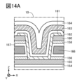
- FIG. 14A is a cross-sectional view of the transistor.
- FIG. 14B is an equivalent circuit diagram of the transistor.
- FIG. 15A is a plan view of the transistor.
- FIG. 15B is a cross-sectional view of the transistor.
- FIG. 15C is a perspective view of the transistor.
- FIG. 15D is an equivalent circuit diagram of a transistor.
- FIG. 15A is a plan view of the transistor.
- FIG. 15B is a cross-sectional view of the transistor.
- FIG. 15C is a perspective view of the transistor.
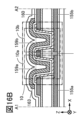
- FIG. 16A is a plan view of the transistor.
- FIG. 16B is a cross-sectional view of the transistor.
- FIG. 16C is a perspective view of the transistor.
- FIG. 16D is an equivalent circuit diagram of a transistor.
- FIG. 17 is a plan view of the signal output circuit.
- FIG. 18 is a plan view of the signal output circuit.
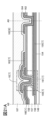
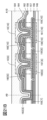
- 19A and 19B are cross-sectional views of the signal output circuit.
- 20A and 20B are cross-sectional views of the signal output circuit.
- 21A and 21B are cross-sectional views of the signal output circuit.
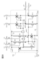
- FIG. 22 is a diagram showing an example of a signal output circuit.
- FIG. 23 is a timing chart for explaining an example of the operation of the signal output circuit.
- FIG. 24 is a circuit diagram for explaining an example of the operation of the signal output circuit.
- FIG. 25 is a circuit diagram for explaining an example of the operation of the signal output circuit.
- FIG. 26 is a circuit diagram for explaining an example of the operation of the signal output circuit.
- FIG. 27 is a circuit diagram for explaining an example of the operation of the signal output circuit.
- FIG. 28 is a circuit diagram for explaining an example of the operation of the signal output circuit.
- FIG. 29 is a circuit diagram for explaining an example of the operation of the signal output circuit.
- FIG. 30 is a circuit diagram for explaining an example of the operation of the signal output circuit.
- FIG. 31 is a diagram showing an example of a signal output circuit.
- FIG. 32 is a diagram showing an example of a signal output circuit.
- FIG. 33 is a timing chart for explaining an example of the operation of the shift register.
- FIG. 33 is a timing chart for explaining an example of the operation of the shift register.
- 34A is a perspective view of the display device.
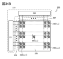
- FIG. 34B is a block diagram of the display device.
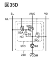
- 35A to 35D are circuit diagrams of pixel circuits.
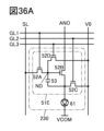
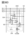
- 36A to 36D are circuit diagrams of pixel circuits.
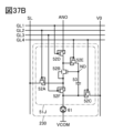
- 37A and 37B are circuit diagrams of pixel circuits.
- 38A and 38B are circuit diagrams of pixel circuits.
- 39A and 39B are diagrams illustrating a configuration example of a drive circuit.
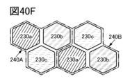
- 40A to 40G are diagrams showing examples of pixels.
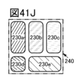
- 41A to 41K are diagrams showing examples of pixels.
- 42A to 42F are diagrams illustrating configuration examples of light emitting devices.
- 43A to 43C are diagrams illustrating configuration examples of light emitting devices.
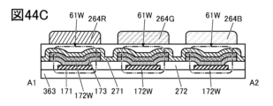
- 44A to 44D are diagrams illustrating configuration examples of light emitting elements.
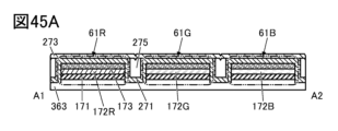
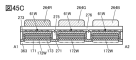
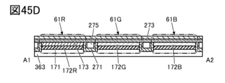
- 45A to 45D are diagrams showing configuration examples of light emitting elements.
- 46A to 46C are diagrams illustrating configuration examples of light emitting elements.
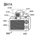
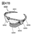
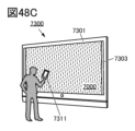
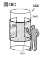
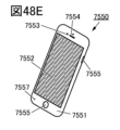
- 47A to 47F are diagrams illustrating an example of an electronic device.
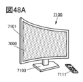
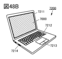
- 48A to 48F are diagrams illustrating an example of an electronic device.
- 49A1 and 49A2 are schematic cross-sectional views of transistors.
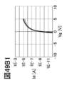
- FIG. 49B1 and FIG. 49B2 are diagrams showing Id-Vg characteristics of a transistor.
- FIGS. 49C1 and 49C2 are diagrams showing Id-Vd characteristics of transistors.
- the resist mask is one that is removed after the etching process is completed. shall be.
- top views also referred to as “top views”
- perspective views descriptions of some components may be omitted.
- some hidden lines may be omitted.
- ordinal numbers such as “first” and “second” are added to avoid confusion of constituent elements, and do not indicate any order or rank such as process order or lamination order. Further, even if a term is not attached with an ordinal number in this specification, etc., an ordinal number may be attached in the claims to avoid confusion of constituent elements. Further, the ordinal numbers used in this specification and the like may be different from the ordinal numbers used in the claims. Further, even if a term is attached with an ordinal number in this specification or the like, the ordinal number may be omitted in the claims or the like.
- the terms “electrode,” “wiring,” and “terminal” do not functionally limit these components.
- an “electrode” may be used as part of a “wiring” and vice versa.
- the terms “electrode” and “wiring” also include a case where a plurality of “electrodes” and “wiring” are provided as one.
- a “terminal” may be used as part of a “wiring” or “electrode,” and vice versa.
- the term “terminal” also includes cases where a plurality of "electrodes", “wirings", “terminals”, etc. are formed integrally.
- an “electrode” can be a part of a “wiring” or a “terminal,” and, for example, a “terminal” can be a part of a “wiring” or a “electrode.”
- terms such as “electrode,” “wiring,” and “terminal” may be replaced with terms such as "region” depending on the case.
- supplying a signal refers to supplying a predetermined potential to a wiring or the like. Therefore, it may be possible to read "signal” as a term such as “potential”. In addition, terms such as “potential” may sometimes be read as “signal.” Further, the "signal” may be a variable potential or a fixed potential. For example, it may be a power supply potential.
- film and “layer” can be interchanged depending on the situation or circumstances.
- conductive layer may be changed to the term “conductive film.”
- insulating film may be changed to the term “insulating layer.”
- a “capacitive element” refers to, for example, a circuit element having a capacitance value higher than 0F, a wiring region having a capacitance value higher than 0F, a parasitic capacitance, or It can be the gate capacitance of a transistor.
- capacitor element can sometimes be replaced with the term “capacitance.”
- capacitor may be translated into the terms “capacitive element,” “parasitic capacitance,” or “gate capacitance.”
- a “capacitor” (including a “capacitor” having three or more terminals) has a configuration including an insulator and a pair of conductive layers sandwiching the insulator.
- a pair of conductive layers in “capacitance” can be translated into a "pair of electrodes," a “pair of conductive regions,” a “pair of regions,” or a “pair of terminals.”
- the term “one of a pair of terminals” may also be referred to as “one terminal” or “first terminal.”
- the term “the other of a pair of terminals” may be referred to as “the other terminal” or “the second terminal.”
- the value of the capacitance can be, for example, 0.05 fF or more and 10 pF or less. Further, for example, it may be set to 1 pF or more and 10 ⁇ F or less.
- source and drain may be interchanged, such as when using transistors of different polarity or when the direction of current changes during circuit operation. Therefore, in this specification and the like, the terms “source” and “drain” can be used interchangeably.
- gate refers to part or all of a gate electrode and a gate wiring.
- the gate wiring refers to a wiring for electrically connecting the gate electrode of at least one transistor to another electrode or another wiring.
- source refers to part or all of a source region, a source electrode, and a source wiring.
- the source region refers to a region of the semiconductor layer where the resistivity is below a certain value.
- a source electrode refers to a conductive layer including a portion connected to a source region.
- the source wiring refers to a wiring for electrically connecting the source electrode of at least one transistor to another electrode or another wiring.
- drain refers to part or all of a drain region, a drain electrode, and a drain wiring.
- the drain region refers to a region of the semiconductor layer where the resistivity is below a certain value.
- a drain electrode refers to a conductive layer including a portion connected to a drain region.
- the drain wiring refers to a wiring for electrically connecting the drain electrode of at least one transistor to another electrode or another wiring.
- the transistors shown in this specification and the like are enhancement type (normally-off type) field effect transistors.
- the transistors described in this specification and the like are n-channel transistors, and unless otherwise specified, the threshold voltage (also referred to as "Vth") of the transistors is greater than 0V.
- the transistor shown in this specification and the like is a p-channel transistor, and unless otherwise specified, the threshold voltage (also referred to as "Vth”) of the transistor is 0V or less.
- the Vth of a plurality of transistors of the same conductivity type are all equal.
- off-state current refers to the current (current) that flows between the source and drain when the transistor is in the off state (also referred to as the "non-conducting state” or “blocking state”).
- drain current also referred to as “drain current” or “Id.”
- an off state is defined as an n-channel transistor in which the potential difference between the gate and source (also referred to as “gate voltage” or “Vg”) with respect to the source is lower than the threshold voltage.
- Vg gate voltage
- the off-state current of an n-channel transistor may refer to the drain current when Vg is lower than Vth.
- off-state current may refer to, for example, a current flowing between a source and a drain when a transistor is in an off state.
- on-current refers to Id when a transistor is in an on-state (also referred to as a "conductive state").
- the on-state refers to a state in which Vg is greater than or equal to Vth for an n-channel transistor, and a state in which Vg is less than or equal to Vth for a p-channel transistor.
- the on-current of an n-channel transistor may refer to the drain current when Vg is equal to or higher than Vth.
- a high power supply potential VDD (hereinafter also simply referred to as “VDD” or “potential H”) indicates a power supply potential higher than the low power supply potential VSS.
- the low power supply potential VSS (hereinafter also simply referred to as “VSS” or “potential L”) indicates a power supply potential lower than the high power supply potential VDD.
- the ground potential GND (hereinafter also simply referred to as “GND”) can also be used as VDD or VSS.
- VDD is GND
- VSS is a potential lower than GND
- VDD is a potential higher than GND. Note that in this specification and the like, VSS is used as a reference potential unless explicitly stated.
- voltage often refers to a potential difference between a certain potential and a reference potential (for example, a ground potential or a source potential). Further, “potential” is relative, and the potential applied to wiring etc. may change depending on the reference potential. Therefore, “voltage” and “potential” may sometimes be interchangeable.
- electrode B does not need to be formed directly on insulating layer A, and there is no need to form another structure between insulating layer A and electrode B. Do not exclude things that contain elements.
- electrode B overlapping insulating layer A is not limited to the state in which electrode B is formed on insulating layer A, but also the state in which electrode B is formed under insulating layer A, or A state in which the electrode B is formed on the right side (or left side) of the insulating layer A is not excluded.
- the terms “adjacent” and “nearby” do not limit that components are in direct contact.
- insulating layer A and electrode B do not need to be formed in direct contact with each other, and other components may be placed between insulating layer A and electrode B. Do not exclude what is included.
- parallel refers to a state in which two straight lines are arranged at an angle of -10° or more and 10° or less. Therefore, the case where the angle is greater than or equal to -5° and less than or equal to 5° is also included.
- substantially parallel or “substantially parallel” refers to a state in which two straight lines are arranged at an angle of -30° or more and 30° or less.
- perpendicular refers to a state in which two straight lines are arranged at an angle of 80° or more and 100° or less. Therefore, the case where the angle is 85° or more and 95° or less is also included.
- substantially perpendicular or “substantially perpendicular” refers to a state in which two straight lines are arranged at an angle of 60° or more and 120° or less.
- the term “the end of the object has a tapered shape” means that the angle formed between the formed surface (bottom surface) and the side surface (surface) in the end region is greater than 0 degrees and less than 90 degrees. , having a cross-sectional shape in which the thickness continuously increases from the end. Further, the taper angle refers to the angle formed between the bottom surface (formed surface) and the side surface (surface) at the end of the object.
- arrows indicating the X direction, Y direction, and Z direction may be attached.
- the "X direction” refers to the direction along the X axis, and the forward direction and reverse direction may not be distinguished unless explicitly stated.
- the X direction, the Y direction, and the Z direction are directions that intersect with each other. More specifically, the X direction, the Y direction, and the Z direction are directions that are orthogonal to each other.
- one of the X direction, the Y direction, or the Z direction may be referred to as a "first direction” or a “first direction.” Further, the other direction may be referred to as a “second direction” or “second direction”. Further, the remaining one may be referred to as a "third direction” or "third direction.”
- the EL layer 172 may be shown divided into an EL layer 172R, an EL layer 172G, an EL layer 172B, and an EL layer 172W.
- the shift register 100 shown in FIG. 1A has n signal output circuits 110 (n is an integer of 1 or more).
- the first stage (first) signal output circuit 110 is sometimes referred to as a signal output circuit 110 [1]
- the nth stage (nth) signal output circuit 110 is sometimes referred to as a signal output circuit 110 [1]. It may be written as 110[n].
- the signal output circuit 110 at the i-th stage may be referred to as a signal output circuit 110[i].
- i an integer from 1 to n
- i an integer from 1 to n
- i an integer from 1 to n
- i an integer from 1 to n
- i- ⁇ an arbitrary number of stages
- i- ⁇ an arbitrary number of stages
- i- ⁇ an arbitrary number of stages
- the shift register 100 also includes two signal output circuits 110 (signal output circuit 110[n+1] and signal output circuit 110[n+2]) which are dummy circuits.
- the terminals, input/output signals, etc. of the signal output circuit 110 may also be described in the same manner as above.
- the signal OUT of the signal output circuit 110[i] may be referred to as the signal OUT[i].
- the shift register 100 also includes wirings 101 to 104 to which four signals CLK (signals CLK_1 to CLK_4), which are clock signals, are supplied, and wirings 105 to which four signals PWC (signals PWC_1 to signals PWC_4) are supplied. to wiring 108.
- a signal CLK_1 is supplied to the wiring 101
- a signal CLK_2 is supplied to the wiring 102
- a signal CLK_3 is supplied to the wiring 103
- a signal CLK_4 is supplied to the wiring 104.
- a signal PWC_1 is supplied to the wiring 105
- a signal PWC_2 is supplied to the wiring 106
- a signal PWC_3 is supplied to the wiring 107
- a signal PWC_4 is supplied to the wiring 108.
- the signal output circuit 110 has terminals 111 to 118 (see FIG. 1B).
- the terminal 111, the terminal 112, and the terminal 113 are each electrically connected to one of the wirings 101 to 104 and a different wiring.
- the first stage signal output circuit 110[1] has a terminal 111 electrically connected to the wiring 101, a terminal 112 electrically connected to the wiring 102, and a terminal 113 electrically connected to the wiring 103. connected. That is, the signal CLK_1 is supplied to the terminal 111, the signal CLK_2 is supplied to the terminal 112, and the signal CLK_3 is supplied to the terminal 113.
- the terminal 111 is electrically connected to the wiring 102
- the terminal 112 is electrically connected to the wiring 103
- the terminal 113 is electrically connected to the wiring 104. ing. That is, the signal CLK_2 is supplied to the terminal 111, the signal CLK_3 is supplied to the terminal 112, and the signal CLK_4 is supplied to the terminal 113.
- the signal CLK_k is supplied to the terminal 111[i] of the signal output circuit 110[i] (see FIG. 1C).
- k is an integer from 1 to 4, and when i is 4 or less, k is equal to i, and when i is 5 or more, k is equal to i-4 ⁇ g.
- g is the quotient of i divided by 4.
- the signal CLK_k+1 is supplied to the terminal 112[i] of the signal output circuit 110[i].
- k is an integer from 1 to 4, and when k+1 is 5, k is set to 1.
- i is 3 or less, k is equal to i, and when i is 4 or more, k is equal to i-4 ⁇ g.
- the signal CLK_k+2 is supplied to the terminal 113[i] of the signal output circuit 110[i].
- k+1 is an integer from 1 to 4, and when k+2 becomes 5, k+2 is set to 1, and when k+2 becomes 6, k+2 is set to 2.
- i is 2 or less, k is equal to i, and when i is 3 or more, k is equal to i-4 ⁇ g.
- terminal 114[i] is electrically connected to the terminal 117[i+1] (not shown) of the next stage signal output circuit 110[i+1] (not shown). Therefore, terminal 117[i] is electrically connected to terminal 114[i-1].
- terminal 114 of signal output circuit 110[1] is electrically connected to terminal 117 of signal output circuit 110[2]. Further, a start pulse SP is supplied to the terminal 117 of the signal output circuit 110[1].
- the terminal 115[i] is electrically connected to the terminal 114[i+2] (not shown) of the signal output circuit 110[i+2] (not shown) two stages later.
- the terminal 115 of the signal output circuit 110[1] is electrically connected to the terminal 114 of the signal output circuit 110[3]
- the terminal 115 of the signal output circuit 110[2] is electrically connected to the terminal 114 of the signal output circuit 110[4]. It is electrically connected to the terminal 114 of. Therefore, the terminal 115 of the signal output circuit 110[n-1] is electrically connected to the terminal 114 of the signal output circuit 110[n+1], and the terminal 115 of the signal output circuit 110[n] is electrically connected to the terminal 114 of the signal output circuit 110[n+1]. n+2] terminal 114. Note that the signal output circuit 110[n+1] and the signal output circuit 110[n+2] do not need to have the terminal 115.
- the terminal 118[i] is electrically connected to any of the wirings 105 to 108.
- the terminal 118 of the signal output circuit 110[1] is electrically connected to the wiring 105
- the terminal 118 of the signal output circuit 110[2] is electrically connected to the wiring 106.
- the signal PWC_k is supplied to the terminal 118[i] of the signal output circuit 110[i].
- k is an integer from 1 to 4, and when i is 4 or less, k is equal to i, and when i is 5 or more, k is equal to i-4 ⁇ g.
- a signal OUT[i] is output from the terminal 116[i].
- the signal OUT[1] is output from the terminal 116 of the signal output circuit 110[1].
- the signal OUT[n] is output from the terminal 116 of the n-th stage signal output circuit 110[n]. Note that "signal OUT[i] is output from terminal 116[i]” can be read as “signal OUT[i] is supplied to terminal 116[i]."
- a signal SROUT[i] is supplied to the terminal 114[i].
- the signal SROUT[i] is output from the terminal 114[i].
- the signal SROUT[1] is output from the terminal 114 of the signal output circuit 110[1].
- the signal SROUT[n] is output from the terminal 114 of the n-th stage signal output circuit 110[n]. Note that "signal SROUT[i] is output from terminal 114[i]” can be read as "signal SROUT[i] is supplied to terminal 114[i]."
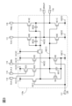
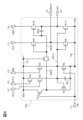
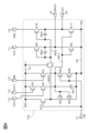
- the signal output circuit 110 includes transistors 10[1] to 10[11] and capacitors 20[1] to 20[3].
- the gate of transistor 10[1] is electrically connected to terminal 117 and the gate of transistor 10[6].
- the source of the transistor 10[1] is electrically connected to the drain of the transistor 10[2], and the drain of the transistor 10[1] is electrically connected to the wiring 131.
- the gate of transistor 10[2] is electrically connected to one terminal of capacitor 20[1].
- the source of transistor 10[2] is electrically connected to the other terminal of capacitor 20[1], the source of transistor 10[6], and wiring 132.
- the gate of the transistor 10[3] is electrically connected to the terminal 113, the drain of the transistor 10[3] is electrically connected to the wiring 131, and the source of the transistor 10[3] is electrically connected to the drain of the transistor 10[4]. electrically connected.
- the gate of transistor 10[4] is electrically connected to terminal 112, and the drain of transistor 10[4] is electrically connected to the source of transistor 10[3].
- the source of transistor 10[4] is electrically connected to the gates of transistor 10[2], transistor 10[9], and transistor 10[11], and one terminal of capacitor 20[1].
- the gates of transistors 10[2], 10[9], and 10[11], the source of transistor 10[4], and one terminal of capacitor 20[1] are electrically connected.
- the area connected to the node ND[1] is called the node ND[1].
- the capacitor 20[1] has a function of suppressing potential fluctuations of the node ND[1] when the node ND[1] is in a floating state and maintaining the potential of the node ND[1].
- the gate of the transistor 10[5] is electrically connected to the terminal 115, and the drain of the transistor 10[5] is electrically connected to the wiring 131.
- the source of transistor 10[5] is electrically connected to the gate of transistor 10[2], the gate of transistor 10[9], the gate of transistor 10[11], and the drain of transistor 10[6].
- the gate of the transistor 10[7] is electrically connected to the wiring 131, and one of the source or drain of the transistor 10[7] is electrically connected to the source of the transistor 10[1] and the drain of the transistor 10[2]. be done.
- the other source or drain of transistor 10[7] is connected to the gate of transistor 10[8], one terminal of capacitor 20[2], the gate of transistor 10[10], and one terminal of capacitor 20[3]. electrically connected.
- node ND[2] a region where one of the source or drain of the transistor 10[7], the source of the transistor 10[1], and the drain of the transistor 10[2] are electrically connected.
- the drain of transistor 10[8] is electrically connected to terminal 111.
- the source of transistor 10[8] is electrically connected to the other terminal of capacitor 20[2], terminal 114, and the drain of transistor 10[9].
- the drain of transistor 10[10] is electrically connected to terminal 118.
- the source of transistor 10[10] is electrically connected to the other terminal of capacitor 20[3], terminal 116, and the drain of transistor 10[11].
- the source of transistor 10[9] and the source of transistor 10[11] are electrically connected to wiring 132.
- drain of transistor 10[1], the drain of transistor 10[3], the drain of transistor 10[5], and the gate of transistor 10[7] may be electrically connected to different wirings.
- source of transistor 10[6], the source of transistor 10[9], and the source of transistor 10[11] may be electrically connected to different wirings.
- the drain of transistor 10[1] is electrically connected to wiring 131[1]
- the drain of transistor 10[3] is electrically connected to wiring 131[2]
- the transistor The drain of transistor 10[5] may be electrically connected to wiring 131[3]
- the gate of transistor 10[7] may be electrically connected to wiring 131[4].
- the source of transistor 10[6] is electrically connected to wiring 132[1]
- the source of transistor 10[9] is electrically connected to wiring 132[2]
- the source of transistor 10[11] is electrically connected to wiring 132[2]. It may be electrically connected to the wiring 132[3]. Note that, as shown in FIG. 4, if a sufficient capacitance value of the capacitor 20[3] can be secured, the formation of the capacitor 20[2] may be omitted.
- a terminal 115 is supplied with a signal RIN, a terminal 117 is supplied with a signal LIN, a terminal 114 is supplied with a signal SROUT, and a terminal 116 is supplied with a signal OUT. Further, in the first stage signal output circuit 110a, the signal CLK_1 is supplied to the terminal 111, the signal CLK_2 is supplied to the terminal 112, the signal CLK_3 is supplied to the terminal 113, and the signal PWC_1 is supplied to the terminal 118.
- the signal CLK_2 is supplied to the terminal 111
- the signal CLK_3 is supplied to the terminal 112
- the signal CLK_4 is supplied to the terminal 113
- the signal PWC_2 is supplied to the terminal 118.
- FIG. 5 shows a circuit diagram of a signal output circuit 110b which is a modification of the signal output circuit 110a.
- the signal output circuit 110b has a configuration in which the transistor 10[4] is removed from the signal output circuit 110a. Further, the source of transistor 10[3] is electrically connected to node ND[1]. By omitting either the transistor 10[3] or the transistor 10[4], it is possible to realize the signal output circuit 110b occupying a small area.
- FIG. 6 shows a circuit diagram of a signal output circuit 110c which is a modification of the signal output circuit 110a.
- Each of the transistor 10[2] and the transistor 10[6] may be a multi-gate transistor.
- FIG. 6 shows an example in which each of the transistor 10[2] and the transistor 10[6] is a double-gate transistor, which is a type of multi-gate transistor.
- the source of transistor 10[2]a is electrically connected to the drain of transistor 10[2]b, and the drain of transistor 10[2]a is connected to the source of transistor 10[1] and the source of transistor 10[7] or Electrically connected to one side of the drain.
- the source of transistor 10[2]b is electrically connected to the other terminal of capacitor 20[1], the source of transistor 10[6]b, and wiring 132.
- the gate of transistor 10[2]a and the gate of transistor 10[2]b are electrically connected. That is, transistor 10[2]a and transistor 10[2]b are connected in series, and both function as one transistor 10[2]. Furthermore, the gate of transistor 10[2]a and the gate of transistor 10[2]b are electrically connected to node ND[1].
- the transistor 10[2] may be a multi-gate transistor configured by connecting three or more transistors in series.
- the source of the transistor 10[6]a is electrically connected to the drain of the transistor 10[6]b, and the drain of the transistor 10[6]a is electrically connected to the node ND[1].
- the source of transistor 10[6]b is electrically connected to the other terminal of capacitor 20[1], the source of transistor 10[2]b, and wiring 132.
- the gate of transistor 10[6]a and the gate of transistor 10[6]b are electrically connected. That is, the transistor 10[6]a and the transistor 10[6]b are connected in series, and both function as one transistor 10[6].
- the gate of transistor 10[6]a and the gate of transistor 10[6]b are electrically connected to the gate of transistor 10[1] and terminal 117.
- the transistor 10[6] may be a multi-gate transistor configured by connecting three or more transistors in series.
- Multi-gate transistors have high dielectric strength between the source and drain. Therefore, the reliability of a circuit using multi-gate transistors can be improved. Therefore, the reliability of a semiconductor device including the circuit can be improved. Multi-gate transistors may be applied to transistors other than transistor 10[2] and transistor 10[6].
- FIG. 7 shows a circuit diagram of a signal output circuit 110d that is a modification of the signal output circuit 110c. Note that the signal output circuit 110d is also a modification of the signal output circuit 110a.
- the signal output circuit 110d includes a transistor 10[12].
- the source of the transistor 10[12] is electrically connected to the node ND[1], and the drain is electrically connected to the wiring 131. Further, the gate of the transistor 10 [12] is electrically connected to the terminal 119.
- a signal INIRES is supplied to terminal 119.
- the signal INIRES functions as a reset signal, and while the potential H is being supplied to the terminal 119 as the signal INIRES, the signal OUT and the signal SROUT are at the potential L.
- the transistor 10[12] is turned on, and the potential of the node ND1 becomes the potential H.
- the transistor 10[9] is turned on, and the potential L is supplied to the terminal 114. Further, the transistor 10 [11] is turned on, and the potential L is supplied to the terminal 116.
- the operation of the signal output circuit 110d can be stopped at any timing.
- FIG. 8 shows a circuit diagram of a signal output circuit 110e that is a modification of the signal output circuit 110a.
- the signal output circuit 110e uses transistors with back gates as the transistor 10[2], the transistor 10[6], the transistor 10[9], and the transistor 10[11].
- the back gates of transistor 10[2], transistor 10[6], transistor 10[9], and transistor 10[11] are electrically connected to terminal 121 via wiring 133.
- a signal SEL is supplied to the terminal 121.
- the signal SEL may have a fixed potential or a variable potential.
- the signal SEL When the signal SEL is set to a fixed potential, it may be the potential L (VSS) or a potential lower than the potential L.
- GBTS Gallium Bias Temperature Stress
- PBTS Positive Bias Temperature Stress
- NBTS Negative Bias Temperature Stress
- PBTS test and NBTS test performed under light irradiation are respectively PBTIS (Positive Bias Temperature Illumination Stress) test and NBTIS (Negative Bias Temperature I) test. Illumination Stress) test.
- n-type transistors In n-type transistors, a positive potential is applied to the gate when the transistor is turned on, so the amount of variation in threshold voltage in the PBTS test is an important indicator of transistor reliability. This is one of the items.
- a negative potential is applied to the gate of a p-type transistor when the transistor is turned on, it is important to pay attention to the amount of variation in the threshold voltage in the NBTS test as an indicator of the reliability of the transistor. This is one of the important items. It can be said that the smaller the amount of variation in threshold voltage before and after the GBTS test, the higher the reliability of the transistor.
- the potential H (VDD) is held at the node ND[1] of the signal output circuit 110 (signal output circuit 110a, etc.) for a long period of time. Therefore, PBTS is applied to transistor 10[2], transistor 10[9], and transistor 10[11] for a long period of time. Furthermore, NBTS is applied to the transistor 10[6] for a long period of time. By using transistors with back gates for transistor 10[2], transistor 10[6], transistor 10[9], and transistor 10[11], deterioration of transistor characteristics due to NBTS and PBTS is suppressed.
- the transistor can be turned off reliably by supplying a potential lower than the potential L to the back gate. can be in a state. Therefore, the potential of node ND[1] can be held reliably. Therefore, the operation of the signal output circuit 110 is stabilized, and the reliability of the semiconductor device including the signal output circuit 110 can be improved.
- the operating speed of the shift register 100 is slow (the driving frequency is low)
- the period during which the node ND[1] and the like are in a floating state becomes long.
- the potential of the node ND[1] etc. can be reliably maintained. Therefore, the operation of the signal output circuit 110 is stabilized, and the reliability of the semiconductor device including the signal output circuit 110 can be improved.
- PBTS is applied to transistor 10[2], transistor 10[9], and transistor 10[11] for a long period of time
- NBTS is applied to transistor 10[6] for a long period of time. Therefore, there is a possibility that the deterioration of transistor characteristics differs between transistor 10[2], transistor 10[9], transistor 10[11], and transistor 10[6].
- the back gates of transistor 10[2], transistor 10[9], and transistor 10[11] are electrically connected to terminal 121 via wiring 133, and transistor 10[ 6] may be electrically connected to the terminal 122 via the wiring 134.
- the signal SEL_A is supplied to the terminal 121 as the signal SEL
- the signal SEL_B is supplied to the terminal 122 as the signal SEL.
- the potential of the signal SEL_A and the potential of the signal SEL_B may be the same or different.
- the transistor characteristics of the transistor 10[2], the transistor 10[9], and the transistor 10[11] and the transistor characteristics of the transistor 10[6] are made different. It's okay.
- the signal SEL_A may be synchronized with the signal RIN. For example, when the signal RIN is at the potential H, the signal SEL_A may be set at the potential H. Further, when the signal RIN is at the potential L, the signal SEL_A may be set to the potential L or a potential lower than the potential L. By setting both the signal SEL_A and the signal RIN to the potential H, the operating speed of the transistor 10[2], the transistor 10[9], and the transistor 10[11] can be increased.
- the signal SEL_B may be synchronized with the signal LIN. For example, when the signal LIN is at the potential H, the signal SEL_B may be set at the potential H. Further, when the signal LIN is at the potential L, the signal SEL_B may be set to the potential L or a potential lower than the potential L. By setting both the signal SEL_B and the signal LIN to the potential H, the operating speed of the transistor 10[6] can be increased.
- FIG. 10 shows a circuit diagram of a signal output circuit 110f that is a modification of the signal output circuit 110c.
- the signal output circuit 110f has a configuration in which a transistor 10 [13] and a transistor 10 [14] are added to the signal output circuit 110c.
- the gate of transistor 10[13] is electrically connected to the source of transistor 10[1], the drain of transistor 10[2]a, and one of the source or drain of transistor 10[7].
- the source of transistor 10[13] is electrically connected to the source of transistor 10[2]a and the drain of transistor 10[2]b.
- the drain of transistor 10[13] is electrically connected to wiring 135.
- the gate of transistor 10[14] is electrically connected to node ND[1].
- the source of transistor 10[14] is electrically connected to the source of transistor 10[6]a and the drain of transistor 10[6]b.
- the drain of transistor 10[14] is electrically connected to wiring 136.
- a potential SMP is supplied to the wiring 135 and the wiring 136.
- the potential SMP is preferably higher than the potential L+Vth, and more preferably higher than the potential L+2 ⁇ Vth.
- potential H (more precisely, potential H-Vth) is supplied to node ND[2]
- transistor 10[13] is turned on, and potential SMP is supplied to the source of transistor 10[2]a. Ru.
- the potential H is supplied to the node ND[1]
- the transistor 10[14] is turned on, and the potential SMP is supplied to the source of the transistor 10[6]a.
- the potential SMP is preferably a fixed potential, but may be a variable potential.
- the signal output circuit 110 (signal output circuit 110a, signal output circuit 110c, and signal output circuit 110d) according to one embodiment of the present invention is a unipolar circuit configured using transistors of the same conductivity type (n-channel type). It is. Since there is no need to use transistors of different conductivity types (p-channel type), manufacturing costs are reduced and a highly productive signal output circuit can be realized. Further, since a process for forming transistors of different conductivity types is not necessary, the manufacturing period is shortened and the yield is improved.
- a p-channel transistor may be used as a part of the signal output circuit 110 if necessary. That is, transistors of different conductivity types may be used as part of the signal output circuit 110.
- the signal output circuit 110 may include a CMOS (Complementary Metal-Oxide-Semiconductor) circuit including an n-channel transistor and a p-channel transistor. Note that although this embodiment shows an example in which the signal output circuit 110 is composed of all n-channel transistors, it is also possible to replace all of these transistors with p-channel transistors.
- CMOS Complementary Metal-Oxide-Semiconductor
- FIG. 11A is a plan view of the transistor 10.
- FIG. 11B is a cross-sectional view of the portion indicated by the dashed line A1-A2 in FIG. 11A.
- FIG. 11C is a perspective view of the transistor 10.
- FIG. 11D is an equivalent circuit diagram of the transistor 10.
- some of the components of the transistor 10 are omitted in FIGS. 11A and 11C.
- the insulating layer 164 shown in FIG. 11B and the like are omitted.
- FIG. 12A and 12B are enlarged views of the transistor 10 shown in FIG. 11B.
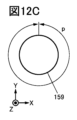
- FIG. 12C is a diagram of the opening 159 viewed from the Z direction.
- the transistor 10 includes an insulating layer 154 over a substrate 153 and a conductive layer 155 over the insulating layer 154. Further, an insulating layer 156 is provided over the conductive layer 155, an insulating layer 157 is provided over the insulating layer 156, and an insulating layer 158 is provided over the insulating layer 157. Further, a conductive layer 160 is provided on the insulating layer 158. In this specification and the like, the insulating layer 156, the insulating layer 157, and the insulating layer 158 may be collectively referred to as the insulating layer 145.
- openings 159 are provided in the conductive layer 160, the insulating layer 158, the insulating layer 157, and the insulating layer 156 in a region overlapping with a part of the conductive layer 155 (see FIG. 11B and FIG. 12A). Further, a semiconductor layer 161 is provided in the opening 159 . The semiconductor layer 161 has a region overlapping with the bottom of the opening 159 and a region overlapping with the side surface of the opening 159. The semiconductor layer 161 has a region in contact with the insulating layer 145 at the opening 159.
- the semiconductor layer 161 has a region in contact with the side surface of the insulating layer 158, a region in contact with the side surface of the insulating layer 157, and a region in contact with the side surface of the insulating layer 156. Further, in the opening 159, a part of the semiconductor layer 161 is in contact with the conductive layer 160, and another part of the semiconductor layer 161 is in contact with the conductive layer 155. That is, a portion of the semiconductor layer 161 is electrically connected to the conductive layer 160, and another portion of the semiconductor layer 161 is electrically connected to the conductive layer 155.
- an insulating layer 162 is provided over the insulating layer 158 , the conductive layer 160 , and the semiconductor layer 161 , and a conductive layer 163 is provided over the insulating layer 162 .
- an insulating layer 164 is provided over the insulating layer 162 and the conductive layer 163.
- the insulating layer 162 has a region that overlaps the side surface of the opening 159 with the semiconductor layer 161 interposed therebetween.
- a conductive layer 163 is provided to cover the semiconductor layer 161. Therefore, conductive layer 163 has a region that extends beyond the edge of semiconductor layer 161. Furthermore, the conductive layer 163 has a region that overlaps with the side surface of the opening 159 via the insulating layer 162 and the semiconductor layer 161.
- the conductive layer 155 has a region that functions as either a source electrode or a drain electrode of the transistor 10. Further, the conductive layer 160 has a region that functions as the other of the source electrode and the drain electrode of the transistor 10. For example, if conductive layer 155 functions as a drain electrode of transistor 10, conductive layer 160 functions as a source electrode of transistor 10.
- the semiconductor layer 161 has a region functioning as a semiconductor layer in which a channel of the transistor 10 is formed, the insulating layer 162 has a region functioning as a gate insulating layer, and the conductive layer 163 has a region functioning as a gate electrode. .
- the transistor 10 is provided in a region including the opening 159.
- the transistor 10 has a source electrode and a drain electrode arranged in the Z direction. Therefore, the source and drain of the transistor 10 are arranged at different positions in the Z direction. For example, when the top surface of the substrate 153 is used as a reference, the source and drain of the transistor 10 are arranged at different distances from the top surface of the substrate 153, which is the reference. Note that being placed at different positions in the Z direction is also referred to as "being placed at different heights.” Such a transistor is also referred to as a “vertical channel transistor,” “vertical channel transistor,” “vertical transistor,” or “VFET (Vertical Field Effect Transistor).” In a vertical channel transistor, the direction in which Id flows includes a component in the Z direction (vertical direction).
- the cross section of the semiconductor layer 161 on the conductive layer 155 when viewed from the X direction or the Y direction is a cross section passing through the center (or center of gravity) of the opening 159 when viewed from the Z direction.
- the angle ⁇ (see FIG. 12A) between the surface to be formed and the flow direction of Id is 5 degrees or more and 110 degrees or less, or 10 degrees or more and 90 degrees or less, or 30 degrees or more and 90 degrees or less, or 60 degrees or more and 90 degrees or less.
- the semiconductor layer 161 has a region in contact with the side surface of the insulating layer 157. Therefore, Id flows along the side surfaces of the insulating layer 157. Therefore, the angle ⁇ between the surface of the semiconductor layer 161 on the conductive layer 155 and the direction in which Id flows can be read as the angle ⁇ between the surface of the semiconductor layer 161 on the conductive layer 155 and the side surface of the insulating layer 157. be able to.
- a vertical channel transistor has a source electrode and a drain electrode arranged in the Z direction, the area occupied by the transistor can be reduced.
- the area occupied by the semiconductor device can be significantly reduced.
- substrate There are no major restrictions on the materials used for the substrate 153 and the substrates 148 and 152 described below. Depending on the purpose, the material may be determined by taking into account the presence or absence of translucency and heat resistance to withstand heat treatment. For example, insulating substrates such as glass substrates such as barium borosilicate glass and aluminoborosilicate glass, ceramic substrates, quartz substrates, and sapphire substrates can be used. Further, a semiconductor substrate, a flexible substrate, a bonded film, a base film, etc. may be used.
- the semiconductor substrate examples include a semiconductor substrate made of silicon or germanium, or a compound semiconductor substrate made of silicon carbide, silicon germanium, gallium arsenide, indium phosphide, zinc oxide, or gallium oxide.
- the semiconductor substrate may be a single crystal semiconductor or a polycrystalline semiconductor.
- Examples of substrates used when the transistor 10 or the like according to one embodiment of the present invention is used in a display device include 6th generation (1500 mm x 1850 mm), 7th generation (1870 mm x 2200 mm), 8th generation (2200 mm x 2400 mm), and Glass substrates with large areas such as 9th generation (2400 mm x 2800 mm) and 10th generation (2950 mm x 3400 mm) can be used. Thereby, a large-sized display device can be manufactured. Furthermore, by increasing the size of the substrate, more display devices can be produced from one substrate, and production costs can be reduced.
- polyesters such as polyethylene terephthalate (PET) and polyethylene naphthalate (PEN), polyacrylonitrile, acrylic resins, polyimide, polymethyl methacrylate, and polycarbonate ( PC), polyethersulfone (PES), polyamide (nylon, aramid, etc.), polysiloxane, cycloolefin resin, polystyrene, polyamideimide, polyurethane, polyvinyl chloride, polyvinylidene chloride, polypropylene, polytetrafluoroethylene (PTFE), ABS resin, cellulose nanofiber, etc. can be used.
- PET polyethylene terephthalate
- PEN polyethylene naphthalate
- PC polycarbonate
- PES polyethersulfone
- polyamide nylon, aramid, etc.
- polysiloxane polystyrene
- polyamideimide polyurethane
- polyvinyl chloride polyvinylidene chloride
- PTFE poly
- a lightweight semiconductor device including the transistor 10 can be provided. Furthermore, by using the above material as a substrate, a semiconductor device that is resistant to impact can be provided. Further, by using the above material as a substrate, a semiconductor device that is less likely to be damaged can be provided.
- the flexible substrate used for the substrate has a lower coefficient of linear expansion, since deformation caused by the environment is suppressed.
- the flexible substrate used for the substrate may be made of a material having a coefficient of linear expansion of, for example, 1 ⁇ 10 ⁇ 3 /K or less, 5 ⁇ 10 ⁇ 5 /K or less, or 1 ⁇ 10 ⁇ 5 /K or less.
- aramid is suitable as a flexible substrate because it has a low coefficient of linear expansion.
- [Conductive layer] Aluminum (Al), chromium (Cr), copper (Cu), Silver (Ag), gold (Au), platinum (Pt), tantalum (Ta), nickel (Ni), titanium (Ti), molybdenum (Mo), tungsten (W), hafnium (Hf), vanadium (V), A metal element selected from niobium (Nb), manganese (Mn), magnesium (Mg), zirconium (Zr), beryllium (Be), etc., an alloy containing the above-mentioned metal elements, or a combination of the above-mentioned metal elements. An alloy or the like can be used.
- a semiconductor such as polycrystalline silicon containing an impurity element such as phosphorus, or a silicide such as nickel silicide may be used.
- the method for forming the conductive material is not particularly limited, and various formation methods such as vapor deposition, atomic layer deposition (ALD), chemical vapor deposition (CVD), sputtering, and spin coating may be used. A method can be used.
- a Cu-X alloy (X is Mn, Ni, Cr, Fe, Co, Mo, Ta, or Ti) may be applied as the conductive material. Since the layer formed of the Cu-X alloy can be processed by a wet etching process, it is possible to suppress manufacturing costs.
- an aluminum alloy containing one or more elements selected from titanium, tantalum, tungsten, molybdenum, chromium, neodymium, and scandium may be used as the conductive material.
- conductive materials that can be used for the conductive layer indium tin oxide, indium oxide containing tungsten oxide, indium zinc oxide containing tungsten oxide, indium oxide containing titanium oxide, indium tin containing titanium oxide, etc.
- Conductive materials with oxygen can also be used, such as oxides, indium zinc oxide, indium tin oxide doped with silicon oxide.
- conductive materials containing nitrogen such as titanium nitride, tantalum nitride, and tungsten nitride can also be used.
- the conductive layer can also have a laminated structure in which a conductive material containing oxygen, a conductive material containing nitrogen, and a material containing the metal element described above are appropriately combined.
- the conductive layer may have a single-layer structure of an aluminum layer containing silicon, a two-layer structure in which a titanium layer is stacked on an aluminum layer, a two-layer structure in which a titanium layer is stacked on a titanium nitride layer, or a tungsten layer on a titanium nitride layer.
- a two-layer structure in which a tungsten layer is laminated on a tantalum nitride layer a two-layer structure in which a tungsten layer is laminated on a tantalum nitride layer, and a three-layer structure in which a titanium layer is laminated, an aluminum layer is laminated on the titanium layer, and a titanium layer is laminated on top of that. good.
- a plurality of conductive layers formed of the above-mentioned conductive materials may be laminated and used.
- the conductive layer may have a laminated structure in which a material containing the aforementioned metal element and a conductive material containing oxygen are combined.
- a layered structure may be used in which a material containing the aforementioned metal element and a conductive material containing nitrogen are combined.
- a laminated structure may be used in which a material containing the aforementioned metal element, a conductive material containing oxygen, and a conductive material containing nitrogen are combined.
- a conductive layer is formed by laminating a conductive layer containing copper on a conductive layer containing at least one of indium or zinc and oxygen, and further laminating a conductive layer containing at least one of indium or zinc and oxygen on top of the conductive layer containing at least one of indium or zinc and oxygen. It may also have a three-layer structure. In this case, it is preferable that the side surfaces of the conductive layer containing copper are also covered with a conductive layer containing at least one of indium or zinc and oxygen. Further, for example, a plurality of conductive layers containing at least one of indium or zinc and oxygen may be stacked and used as the conductive layer.
- Each insulating layer includes aluminum nitride, aluminum oxide, aluminum nitride oxide, aluminum oxynitride, magnesium oxide, silicon nitride, silicon oxide, silicon nitride oxide, silicon oxynitride, gallium oxide, germanium oxide, yttrium oxide, zirconium oxide, and lanthanum oxide.
- An insulating material selected from , neodymium oxide, hafnium oxide, tantalum oxide, aluminum silicate, etc. is used in a single layer or in a stacked manner. Alternatively, a mixture of a plurality of materials among oxide materials, nitride materials, oxynitride materials, and nitrided oxide materials may be used.
- the method for forming the insulating material is not particularly limited, and various methods such as vapor deposition, ALD, CVD, sputtering, and spin coating can be used.
- nitrided oxide refers to a material containing more nitrogen than oxygen.
- oxynitride refers to a material containing more oxygen than nitrogen. Note that the content of each element can be measured using, for example, Rutherford Backscattering Spectrometry (RBS).
- RBS Rutherford Backscattering Spectrometry
- the insulating layer 154 and the insulating layer 164 are preferably formed using an insulating material through which impurities hardly pass.
- insulating materials containing boron, carbon, nitrogen, oxygen, fluorine, magnesium, aluminum, silicon, phosphorous, chlorine, argon, gallium, germanium, yttrium, zirconium, lanthanum, neodymium, hafnium or tantalum, in a single layer or It may be used in a laminated manner.
- Examples of insulating materials that are difficult for impurities to pass through include aluminum oxide, aluminum nitride, aluminum oxynitride, aluminum nitride oxide, gallium oxide, germanium oxide, yttrium oxide, zirconium oxide, lanthanum oxide, neodymium oxide, hafnium oxide, tantalum oxide, Examples include silicon nitride.
- the reliability of the semiconductor device including the transistor 10 can be improved.
- an insulating material through which impurities are difficult to pass through for the insulating layer 154 diffusion of impurities from the substrate 153 side can be suppressed, and reliability of the transistor 10 can be improved. That is, the reliability of the semiconductor device including the transistor 10 can be improved.
- an insulating material through which impurities hardly pass through the insulating layer 164 diffusion of impurities from above the insulating layer 164 can be suppressed, and the reliability of the transistor 10 can be improved. That is, the reliability of the semiconductor device including the transistor 10 can be improved.
- an insulating layer that can function as a planarization layer may be used as the insulating layer.
- the material for the insulating layer that functions as the planarization layer include acrylic resin, polyimide, epoxy resin, polyamide, polyimide amide, siloxane resin, benzocyclobutene resin, phenol resin, and precursors thereof.
- low dielectric constant materials low-k materials
- siloxane resins PSG (phosphorus glass), BPSG (phosphorus boron glass), etc.
- a plurality of insulating layers formed of these materials may be stacked.
- the siloxane resin corresponds to a resin containing Si-O-Si bonds formed using a siloxane-based material as a starting material.
- an organic group for example, an alkyl group or an aryl group
- a fluoro group may be used as a substituent. Further, the organic group may have a fluoro group.
- CMP treatment may be performed on the surface of the insulating layer or the like. By performing the CMP treatment, it is possible to reduce the unevenness of the surface of the insulating layer, etc., and improve the coverage of the insulating layer and conductive layer that will be formed later.
- the semiconductor layer 161 a single crystal semiconductor, a polycrystalline semiconductor, a microcrystalline semiconductor, an amorphous semiconductor, or the like can be used alone or in combination.
- the semiconductor material for example, a semiconductor material having a band gap (semiconductor material that is not a zero-gap semiconductor) such as silicon or germanium can be used.
- a semiconductor material having a band gap semiconductor material that is not a zero-gap semiconductor
- silicon or germanium silicon or germanium
- the compound semiconductor an organic substance having semiconductor characteristics or a metal oxide having semiconductor characteristics (also referred to as an oxide semiconductor) can be used. Note that these semiconductor materials may contain impurities as dopants.
- the semiconductor layer 161 may be made of single crystal silicon, polycrystalline silicon, microcrystalline silicon, or amorphous silicon.
- polycrystalline silicon for example, low temperature polysilicon (LTPS) may be used.
- a transistor using amorphous silicon for the semiconductor layer 161 can be formed over a large glass substrate and can be manufactured at low cost.
- a transistor using polycrystalline silicon for the semiconductor layer 161 has high field effect mobility and can operate at high speed.
- a transistor using microcrystalline silicon for the semiconductor layer 161 has higher field effect mobility than a transistor using amorphous silicon, and can operate at high speed.
- Compound semiconductors that can be used as semiconductor materials include silicon carbide, silicon germanium, gallium arsenide, indium phosphide, boron nitride, and boron arsenide.
- Boron nitride that can be used for the semiconductor layer preferably includes an amorphous structure.
- Boron arsenide that can be used in the semiconductor layer preferably contains crystals with a cubic crystal structure.
- the semiconductor layer 161 may include a layered material that functions as a semiconductor.
- a layered material is a general term for a group of materials having a layered crystal structure.
- a layered crystal structure is a structure in which layers formed by covalent bonds or ionic bonds are laminated via bonds that are weaker than covalent bonds or ionic bonds, such as van der Waals forces.
- a layered material has high electrical conductivity within a unit layer, that is, high two-dimensional electrical conductivity. By using a material that functions as a semiconductor and has high two-dimensional electrical conductivity for the channel formation region, a transistor with high on-state current can be provided.
- Examples of the layered material include graphene, silicene, boron carbonitride, and chalcogenide.
- boron carbonitride as a layered material, carbon atoms, nitrogen atoms, and boron atoms are arranged in a hexagonal lattice structure on a plane.
- a chalcogenide is a compound containing chalcogen.
- chalcogen is a general term for elements belonging to Group 16, and includes oxygen, sulfur, selenium, tellurium, polonium, and livermorium.
- examples of chalcogenides include transition metal chalcogenides, group 13 chalcogenides, and the like.
- transition metal chalcogenides that can be used as semiconductor layers of transistors include molybdenum sulfide (typically MoS 2 ), molybdenum selenide (typically MoSe 2 ), and molybdenum tellurium (typically MoTe 2 ) .
- MoS 2 molybdenum sulfide
- MoSe 2 molybdenum selenide
- MoTe 2 molybdenum tellurium
- tungsten sulfide typically WS 2
- tungsten selenide typically WSe 2
- tungsten tellurium typically WTe 2
- hafnium sulfide typically HfS 2
- hafnium selenide typically HfSe 2
- zirconium sulfide typically ZrS 2
- zirconium selenide typically ZrSe 2
- ZrSe 2 zirconium selenide
- an oxide semiconductor has a band gap of 2 eV or more
- a transistor (also referred to as an "OS transistor") using an oxide semiconductor, which is a type of metal oxide, for the semiconductor layer in which a channel is formed has an off-state current of are significantly less. Therefore, power consumption of a semiconductor device including an OS transistor can be reduced.
- the OS transistor operates stably even in a high-temperature environment, with little variation in characteristics. For example, the off-state current hardly increases even in a high-temperature environment. Specifically, the off-state current hardly increases even under an environmental temperature of room temperature or higher and 200° C. or lower. Furthermore, the on-state current is less likely to decrease even in a high-temperature environment. Therefore, a semiconductor device including an OS transistor operates stably even in a high-temperature environment and has high reliability.
- an OS transistor as the transistor 10. Since the OS transistor has a high dielectric strength voltage between the source and the drain, the channel length can be shortened. Therefore, the on-state current can be increased.
- the OS transistor is suitable for a vertical channel type transistor.
- the channel length is 5 nm or more, 7 nm or more, or 10 nm or more, but less than 3 ⁇ m, 2.5 ⁇ m or less, 2 ⁇ m or less, 1.5 ⁇ m or less, 1.2 ⁇ m or less, 1 ⁇ m or less, 500 nm or less, 300 nm or less, or 200 nm.
- the thickness may be 100 nm or less, 50 nm or less, 30 nm or less, or 20 nm or less.
- the channel length L can be set to 100 nm or more and 1 ⁇ m or less.
- the metal oxide contains at least indium (In) or zinc (Zn).
- the metal oxide has two or three selected from indium, element M, and zinc.
- the element M is a metal element or a metalloid element that has a high bonding energy with oxygen, for example, a metal element or a metalloid element that has a higher bonding energy with oxygen than indium.
- the element M includes aluminum, gallium, tin, yttrium, titanium, vanadium, chromium, manganese, iron, cobalt, nickel, zirconium, molybdenum, hafnium, tantalum, tungsten, lanthanum, cerium, neodymium, magnesium, and calcium. , strontium, barium, boron, silicon, germanium, and antimony.
- the element M included in the metal oxide is preferably one or more of the above elements, more preferably one or more selected from aluminum, gallium, tin, and yttrium, and further gallium. preferable. Note that in this specification, etc., metal elements and metalloid elements may be collectively referred to as "metal elements," and the "metal elements" described in this specification, etc. may include semimetal elements.
- indium zinc oxide In-Zn oxide
- indium tin oxide In-Sn oxide
- indium titanium oxide In-Ti oxide
- indium gallium oxide In-Ga oxide
- Indium gallium aluminum oxide In-Ga-Al oxide
- indium gallium tin oxide In-Ga-Sn oxide
- gallium zinc oxide Ga-Zn oxide, also referred to as GZO
- aluminum zinc oxide also written as Al-Zn oxide, AZO
- indium aluminum zinc oxide also written as In-Al-Zn oxide, IAZO
- indium tin zinc oxide In-Sn-Zn oxide
- indium titanium zinc oxide In-Ti-Zn oxide
- indium gallium zinc oxide also referred to as In-Ga-Zn oxide, IGZO
- indium gallium tin zinc oxide In-Ga-Sn-Zn oxide, also referred to as IGZTO)
- indium gallium aluminum zinc oxide also referred to as In-Ga-A
- the field effect mobility of the transistor can be increased.
- the metal oxide may contain one or more metal elements having a large number of periods instead of or in addition to indium.
- metal elements having a large number of periods include metal elements belonging to the fifth period and metal elements belonging to the sixth period.
- Specific examples of the metal element include yttrium, zirconium, silver, cadmium, tin, antimony, barium, lead, bismuth, lanthanum, cerium, praseodymium, neodymium, promethium, samarium, and europium. Note that lanthanum, cerium, praseodymium, neodymium, promethium, samarium, and europium are called light rare earth elements.
- the metal oxide may contain one or more types of nonmetallic elements.
- the metal oxide contains a nonmetal element, the field effect mobility of the transistor can be increased in some cases.
- nonmetallic elements include carbon, nitrogen, phosphorus, sulfur, selenium, fluorine, chlorine, bromine, and hydrogen.
- the metal oxide becomes highly crystalline, and impurities in the metal oxide can be reduced. It can suppress the spread. Therefore, fluctuations in the electrical characteristics of the transistor are suppressed, and reliability can be improved.
- the electrical characteristics and reliability of a transistor vary depending on the composition of the metal oxide applied to the semiconductor layer. Therefore, by varying the composition of the metal oxide depending on the electrical characteristics and reliability required of the transistor, a semiconductor device that has both excellent electrical characteristics and high reliability can be realized.
- the atomic ratio of indium is greater than or equal to the atomic ratio of zinc.
- the atomic ratio of indium is greater than or equal to the atomic ratio of tin.
- a metal oxide in which the atomic ratio of indium is higher than the atomic ratio of tin can be used. Furthermore, it is preferable to use a metal oxide in which the atomic ratio of zinc is higher than the atomic ratio of tin.
- a metal oxide in which the atomic ratio of indium is higher than the atomic ratio of aluminum can be used. Furthermore, it is preferable to use a metal oxide in which the atomic ratio of zinc is higher than that of aluminum.
- a metal oxide in which the atomic ratio of indium to the number of atoms of the metal element is higher than the atomic ratio of gallium can be used. Furthermore, it is more preferable to use a metal oxide in which the atomic ratio of zinc is higher than the atomic ratio of gallium.
- a metal oxide in which the atomic ratio of indium to the number of atoms of the metal element is higher than the atomic ratio of the element M can be used. Furthermore, it is more preferable to use a metal oxide in which the atomic ratio of zinc is higher than the atomic ratio of element M.
- the sum of the atomic ratios of the metal elements can be the atomic ratio of the element M.
- the atomic ratio of the element M can be the sum of the atomic ratio of gallium and the atomic ratio of aluminum.
- the atomic ratio of indium, element M, and zinc is within the above range.
- the ratio of the number of atoms of indium to the sum of the number of atoms of metal elements is 30 atom % or more and 100 atom % or less, preferably 30 atom % or more and 95 atom % or less, more preferably is from 35 atom % to 95 atom %, more preferably from 35 atom % to 90 atom %, more preferably from 40 atom % to 90 atom %, more preferably from 45 atom % to 90 atom %, more preferably from 50 atom % to 90 atom %.
- the ratio of the number of indium atoms to the total number of atoms of indium, element M, and zinc is within the above range.
- the field effect mobility of the transistor can be increased by increasing the ratio of the number of indium atoms to the sum of the number of atoms of the metal elements.
- a circuit that can operate at high speed can be manufactured. Furthermore, it becomes possible to reduce the area occupied by the circuit. For example, when applying the transistor to a large display device or a high-definition display device, even if the number of wires increases, signal delay in each wire can be reduced, and display unevenness can be suppressed. . Furthermore, since the area occupied by the circuit can be reduced, the frame of the display device can be made narrower.
- the analysis of the composition of the composition of metal oxides for example, the energy distributed X -ray optical method (EDX: ENERGY DISPERSIVE X -RAY SPECTROSCOPY), X -ray optical electron division of light (XPS: X -Ray PhotoElECTRON SPECTROSCOP). Y), guidance bond plasma mass analysis method (ICP-MS: Inductively Coupled Plasma-Mass Spectrometry), or Inductively Coupled Plasma-Atomic Emis (ICP-AES) sion Spectrometry) can be used. Alternatively, analysis may be performed by combining two or more of these methods. Note that for elements with low content rates, the actual content rate and the content rate obtained by analysis may differ due to the influence of analysis accuracy. For example, when the content of element M is low, the content of element M obtained by analysis may be lower than the actual content.
- a sputtering method or an ALD method is suitable for forming the metal oxide.
- the atomic ratio of the target and the atomic ratio of the metal oxide may be different.
- the atomic ratio of the metal oxide may be smaller than the atomic ratio of the target.
- the atomic ratio of zinc contained in the target may be about 40% or more and 90% or less.
- a transistor with high reliability against application of a positive bias can be obtained.
- a transistor with a small threshold voltage variation in the PBTS test can be obtained.
- the gallium content is lower than the indium content.
- One of the factors that causes the threshold voltage to fluctuate in the PBTS test is the defect level at or near the interface between the semiconductor layer and the gate insulating layer.
- gallium contained in metal oxides has a property of attracting oxygen more easily than other metal elements (for example, indium or zinc). Therefore, it is presumed that at the interface between the metal oxide containing a large amount of gallium and the gate insulating layer, gallium combines with excess oxygen in the gate insulating layer, making it easier to generate carrier (electron in this case) trap sites. . Therefore, when a positive potential is applied to the gate, carriers are trapped at the interface between the semiconductor layer and the gate insulating layer, which may cause the threshold voltage to fluctuate.
- a metal oxide in which the atomic ratio of indium is higher than the atomic ratio of gallium can be applied to the semiconductor layer.
- a metal oxide in which the atomic ratio of zinc is higher than the atomic ratio of gallium it is preferable to apply a metal oxide in which the atomic ratio of metal elements satisfies In>Ga and Zn>Ga to the semiconductor layer.
- the ratio of the number of gallium atoms to the number of atoms of the metal element contained is greater than 0 atom % and less than 50 atom %, preferably from 0.1 atom % to 40 atom %, more preferably 0.1 atomic % or more and 35 atomic % or less, more preferably 0.1 atomic % or more and 30 atomic % or less, more preferably 0.1 atomic % or more and 25 atomic % or less, more preferably 0.1 atomic % or more and 20 atomic % or less % or less, more preferably 0.1 atomic % or more and 15 atomic % or less, more preferably 0.1 atomic % or more and 10 atomic % or less.
- a metal oxide that does not contain gallium may be applied to the semiconductor layer of the OS transistor.
- In--Zn oxide can be applied to the semiconductor layer.
- the field effect mobility of the transistor can be increased by increasing the ratio of the number of atoms of indium to the number of atoms of the metal element contained in the metal oxide.
- the metal oxide becomes highly crystalline, which suppresses fluctuations in the electrical characteristics of the transistor and increases reliability. be able to.
- a metal oxide that does not contain gallium and zinc, such as indium oxide may be applied to the semiconductor layer. By using a metal oxide that does not contain gallium, it is possible to make threshold voltage fluctuations extremely small, especially in PBTS tests.
- an oxide containing indium and zinc can be used for the semiconductor layer.
- the present invention can also be applied to a case where element M is used instead of gallium. It is preferable to use a metal oxide in which the atomic ratio of indium is higher than the atomic ratio of element M to the semiconductor layer. Further, it is preferable to use a metal oxide in which the atomic ratio of zinc is higher than the atomic ratio of element M.
- the electrical characteristics of the transistor may change.
- a transistor applied to a region where light can enter has small fluctuations in electrical characteristics under light irradiation and high reliability against light. Reliability with respect to light can be evaluated, for example, by the amount of variation in threshold voltage in an NBTIS test.
- a transistor with high reliability against light can be obtained.
- a transistor whose threshold voltage fluctuates in the NBTIS test can be small.
- a metal oxide in which the atomic ratio of element M is greater than or equal to that of indium has a larger band gap, which can reduce the amount of variation in threshold voltage in transistor NBTIS tests.
- the band gap of the metal oxide of the semiconductor layer is preferably 2.0 eV or more, more preferably 2.5 eV or more, further preferably 3.0 eV or more, further preferably 3.2 eV or more, and still more preferably 3.0 eV or more. It is preferably 3 eV or more, more preferably 3.4 eV or more, and even more preferably 3.5 eV or more.
- the ratio of the number of atoms of the element M to the number of atoms of the metal element contained is 20 atom % or more and 70 atom % or less, preferably 30 atom % or more and 70 atom % or less, more preferably 30 atom %.
- Metal oxides having a content of at least 40 at % and no more than 60 at %, more preferably at least 40 at % and no more than 60 at %, and even more preferably at least 50 at % and no more than 60 at % are suitable.
- a metal oxide can be used in which the atomic ratio of indium to the number of atoms of the metal element is equal to or lower than the atomic ratio of gallium.
- the ratio of the number of gallium atoms to the number of atoms of the metal element contained is 20 atom % or more and 60 atom % or less, preferably 20 atom % or more and 50 atom % or less, more preferably 30 atom % or more.
- Suitable metal oxides have a content of 50 at % or less, more preferably 40 at % or more and 60 at % or less, and more preferably 50 at % or more and 60 at % or less.
- the semiconductor layer may have a stacked structure having two or more metal oxide layers.
- the two or more metal oxide layers included in the semiconductor layer may have the same or approximately the same composition.
- the same sputtering target can be used to form the layers, thereby reducing manufacturing costs.
- the two or more metal oxide layers included in the semiconductor layer may have different compositions.
- the element M it is particularly preferable to use gallium or aluminum. For example, using a laminated structure of one selected from indium oxide, indium gallium oxide, and IGZO and one selected from IAZO, IAGZO, and ITZO (registered trademark), etc. Good too.
- a first metal oxide layer having a composition of In:M:Zn 1:1:1 [atomic ratio] or a composition close to that, and an In:Zn layer provided on the first metal oxide layer.
- a metal oxide layer having crystallinity As the semiconductor layer, a metal oxide layer having crystallinity can be used.
- a metal oxide layer having a CAAC (c-axis aligned crystal) structure, a polycrystalline structure, a microcrystalline (NC: nano-crystal) structure, etc. can be used.
- a crystalline metal oxide layer As a semiconductor layer, the density of defect levels in the semiconductor layer can be reduced, and a highly reliable display device can be realized.
- the semiconductor layer of the OS transistor may have a stacked structure of two or more metal oxide layers having different crystallinity.
- the layered structure includes a first metal oxide layer and a second metal oxide layer provided on the first metal oxide layer, and the second metal oxide layer
- the structure can include a region having higher crystallinity than the oxide layer.
- the second metal oxide layer may have a region having lower crystallinity than the first metal oxide layer.
- the two or more metal oxide layers included in the semiconductor layer may have the same or approximately the same composition.
- a stacked structure of two or more metal oxide layers having different crystallinity can be formed.
- the two or more metal oxide layers included in the semiconductor layer may have different compositions.
- the channel length L is determined by the thickness of the insulating layer provided between the conductive layer 160 and the conductive layer 155. Therefore, a transistor with a short channel length L can be manufactured with high precision. Furthermore, variations in characteristics among the plurality of transistors 10 are also reduced. Therefore, the operation of the semiconductor device including the transistor 10 is stabilized, and reliability can be improved. Further, when characteristic variations are reduced, the degree of freedom in circuit design of the semiconductor device increases, and the operating voltage can also be reduced. Therefore, power consumption of the semiconductor device can be reduced.
- a material containing hydrogen is preferably used for the insulating layer 156 and the insulating layer 158.
- the oxide semiconductor in the region in contact with the insulating layer is made n-type and can function as a source region or a drain region.
- a material containing silicon, nitrogen, and hydrogen may be used as the insulating layer.
- silicon nitride containing hydrogen, silicon nitride oxide containing hydrogen, or the like may be used.
- the conductive layer 155 in contact with the semiconductor layer 161 and the conductive layer 160 in contact with the semiconductor layer 161 can be formed using a conductive material that converts the oxide semiconductor into n-type.
- a conductive material containing nitrogen may be used.
- a conductive material containing titanium or tantalum and nitrogen may be used.
- another conductive material may be provided over the conductive material containing nitrogen.
- a material containing reduced hydrogen and oxygen for the insulating layer 157.
- a material containing silicon and oxygen may be used. Specifically, silicon oxide, silicon oxynitride, or the like may be used. Since hydrogen is an impurity element in an oxide semiconductor, the semiconductor layer 161 that is an oxide semiconductor and the insulating layer 157 with reduced hydrogen are in contact with each other, making it difficult for the semiconductor layer 161 to become n-type. Further, because the semiconductor layer 161 that is an oxide semiconductor and the insulating layer 157 containing oxygen are in contact with each other, oxygen vacancies in the semiconductor layer 161 are reduced, the characteristics of the transistor 10 are stabilized, and reliability is improved.
- the insulating layer 157 preferably contains excess oxygen.
- excess oxygen refers to oxygen released by heating.
- a material containing excess oxygen it is preferable that a material through which oxygen does not easily permeate is used for the insulating layer 156 and the insulating layer 158.
- an oxide containing one or both of aluminum and hafnium, silicon nitride, and the like can be used as the material that is difficult for oxygen to pass through.
- an insulating layer containing silicon and oxygen may be provided between two insulating layers (insulating layer 156, insulating layer 158) containing silicon and nitrogen.
- the region of the semiconductor layer 161 in contact with the conductive layer 160 and the region of the semiconductor layer 161 in contact with the insulating layer 158 functions as either a source (source region) or a drain (drain region).
- a region of the semiconductor layer 161 in contact with the conductive layer 155 and a region of the semiconductor layer 161 in contact with the insulating layer 156 function as the other of the source (source region) and the drain (drain region). Therefore, the channel length L of the transistor 10 is determined by the thickness t of the insulating layer 157 (see FIG. 12A).
- the insulating layer 156 and the insulating layer 158 may be made of a material that does not contain hydrogen or contains very little hydrogen.
- silicon nitride with extremely low hydrogen content or silicon nitride oxide with extremely low hydrogen content may be used.
- the region where the semiconductor layer 161 contacts the insulating layer 156 and the region where the semiconductor layer 161 contacts the insulating layer 158 are not converted to n-type. Therefore, a region of the semiconductor layer 161 in contact with the conductive layer 160 functions as either a source (source region) or a drain (drain region). Further, a region of the semiconductor layer 161 in contact with the conductive layer 155 functions as the other of a source (source region) and a drain (drain region).
- the total thickness ts of the insulating layer 156, the insulating layer 157, and the insulating layer 158 corresponds to the channel length L of the transistor 10 (see FIG. 12A).
- the channel length L can be controlled by adjusting the thicknesses of the insulating layer 156, the insulating layer 157, and the insulating layer 158.
- the channel length L is 5 nm or more, 7 nm or more, or 10 nm or more, but less than 3 ⁇ m, 2.5 ⁇ m or less, 2 ⁇ m or less, 1.5 ⁇ m or less, 1.2 ⁇ m or less, 1 ⁇ m or less, 500 nm or less, 300 nm or less, It can be 200 nm or less, 100 nm or less, 50 nm or less, 30 nm or less, or 20 nm or less.
- the channel length L can be set to 100 nm or more and 1 ⁇ m or less.
- insulating layer 156 insulating layer 156, insulating layer 157, and insulating layer 1528 are provided between conductive layer 155 and conductive layer 160 is shown;
- the number of insulating layers between layers 160 is not limited to this.
- the number of insulating layers between the conductive layer 155 and the conductive layer 160 may be one or two layers, or may be four or more layers.
- the circumferential length p of the opening 159 becomes the channel width W of the transistor 10 (see FIG. 12C).
- the circumferential length p may be determined, for example, at a position at half the thickness t (t/2) of the insulating layer 157 or at a position at half the thickness ts (ts/2).
- the circumferential length of any position of the opening 159 may be set as the channel width W.
- the circumferential length p at the bottom of the opening 159 may be the channel width W
- the circumferential length p at the top of the opening 159 may be the channel width W.
- the outline (planar shape) of the opening 159 viewed from the Z direction is shown as a circle, but the shape is not limited to this.
- the outline of the opening 159 viewed from the Z direction may be elliptical (see FIG. 12D) or rectangular (see FIG. 12E).
- FIG. 12E shows a rectangle with curved corners.
- the outline of the opening 159 when viewed from the Z direction may have a shape including one or both of a straight part and a curved part (see FIG. 12F).
- the capacitance value of the parasitic capacitance occurring between the gate and the source is different from the capacitance value of the parasitic capacitance occurring between the gate and the drain.
- the capacitance value of capacitance C1 is the capacitance C1 that occurs in the region where conductive layer 160 and conductive layer 163 overlap on insulating layer 145, and the capacitance C2 that occurs in the region where conductive layer 155 and conductive layer 163 overlap in opening 159. becomes larger than the capacitance value of the capacitor C2 (see FIG. 11D and FIG. 12B).
- FIG. 13A and 13B show plan views similar to FIG. 11A.
- the conductive layer 163 overlaps with the conductive layer 160 at the periphery of the opening 159 so as to surround the opening 159, and overlaps with the conductive layer 160 at the bottom of the opening 159.
- FIG. 13A the region functioning as the capacitor C1 when viewed from the Z direction is hatched.
- FIG. 13B the region functioning as the capacitor C2 when viewed from the Z direction is hatched.
- a region where the conductive layer 155 and the conductive layer 163 overlap with each other via the semiconductor layer 161 and the insulating layer 162 functions as a capacitor C2 (see FIGS. 12B and 13B).
- the insulating layer 145 and the insulating layer 162 are not illustrated in FIG. 13B.
- the area of the region functioning as the capacitor C1 is larger than the area of the region functioning as the capacitor C2.
- the capacitance value of the capacitor C1 becomes larger than that of the capacitor C2.
- the shape of the opening 159 will be changed, and the circumferential length p of the opening 159 will change. Since a change in the circumferential length p directly affects the electrical characteristics of the transistor 10, it is difficult to adjust the capacitance value of the capacitor C2.
- the overlapping area of the conductive layer 163 and the conductive layer 160 can be easily adjusted, and the electrical characteristics of the transistor 10 are hardly affected.
- the capacitance value of the capacitor C1 can be increased.
- a conductive layer 166 close to the semiconductor layer 161 may be provided in the insulating layer 157. Further, the conductive layer 166 is provided without contacting the semiconductor layer 161. Further, the conductive layer 166 is preferably provided surrounding the semiconductor layer 161. By providing the conductive layer 166 close to the semiconductor layer 161 without being in contact with the semiconductor layer 161, the conductive layer 166 can function as a back gate electrode of the transistor 10. Therefore, the transistor 10 shown in FIG. 14A functions as a transistor having a back gate (back gate electrode). Note that FIG. 14B is an equivalent circuit diagram of the transistor 10 shown in FIG. 14A.
- the back gate electrode will be explained.
- the back gate electrode is formed of a conductive layer, and is arranged so that the channel forming region of the semiconductor layer is sandwiched between the gate electrode and the back gate electrode. Therefore, the back gate electrode can function similarly to the gate electrode.
- the potential of the back gate electrode may be the same potential as that of the gate electrode, or may be a GND potential or an arbitrary potential.
- the threshold voltage of the transistor can be changed by changing the potential of the back gate electrode independently of the potential of the gate electrode instead of making it the same as that of the gate electrode.
- the gate electrode and the back gate electrode are formed of a conductive layer, they have a function of preventing an electric field generated outside the transistor from acting on the channel formation region of the semiconductor layer (particularly an electric field shielding function against static electricity, etc.). As a result, variations in characteristics among transistors are reduced. Further, deterioration of transistor characteristics due to the GBTS test is suppressed. For example, by having a back gate electrode, fluctuations in threshold voltage before and after a GBTS test can be suppressed. Further, a transistor having a back gate electrode has a smaller change in threshold voltage before and after a GBTS test than a transistor having no back gate electrode.
- the GBTS (NBTS and PBTS) test is a type of accelerated test, and can evaluate changes in transistor characteristics (changes over time) caused by long-term use in a short time.
- the amount of variation in the threshold voltage of a transistor before and after a GBTS test is an important index for examining reliability. It can be said that the smaller the amount of variation in the threshold voltage before and after the GBTS test, the more reliable the transistor is.
- the back gate electrode side when light is incident from the back gate electrode side, by forming the back gate electrode with a conductive film having a light-blocking property, it is possible to prevent light from entering the semiconductor layer from the back gate electrode side.
- the gate electrode by forming the gate electrode using a conductive film having light-blocking properties, it is possible to prevent light from entering the semiconductor layer from the gate electrode side.
- photodeterioration of the semiconductor layer is prevented, and deterioration of electrical characteristics such as a shift in the threshold voltage of the transistor is prevented. Can be done.
- the gate electrode and the back gate electrode can block the electric field generated from the drain electrode from acting on the semiconductor layer. Therefore, it is possible to suppress fluctuations in the rise voltage of the on-current caused by fluctuations in the drain voltage. Note that this effect occurs significantly when a potential is supplied to the gate electrode and the back gate electrode.
- the apparent channel width W of the transistor 10 can be increased.
- the resistance value between the source and drain when the transistor 10 is in the on state becomes smaller, and Id when the transistor 10 is in the on state can be increased.
- FIG. 15A is a plan view of transistor 10 including transistor 10a and transistor 10b.
- FIG. 15B is a cross-sectional view of the portion indicated by the dashed line A1-A2 in FIG. 15A.
- FIG. 15C is a perspective view of transistor 10 including transistor 10a and transistor 10b.
- FIG. 15D is an equivalent circuit diagram of transistor 10 including transistor 10a and transistor 10b. In order to make it easier to understand the configuration of the transistor 10, some of the components of the transistor 10 are omitted in FIGS. 15A and 15C.
- Transistor 10a and transistor 10b have the same configuration as transistor 10 described using FIGS. 11 and 12.
- Transistor 10a is provided in a region including opening 159a
- transistor 10b is provided in a region including opening 159b. Opening 159a and opening 159b can be formed similarly to opening 159.
- a part of the conductive layer 155 functions as one of the source electrode or the drain electrode of the transistor 10a, and another part of the conductive layer 155 functions as one of the source electrode or the drain electrode of the transistor 10b. Further, a part of the conductive layer 160 functions as the other of the source electrode or the drain electrode of the transistor 10a, and another part of the conductive layer 160 functions as the other of the source electrode or the drain electrode of the transistor 10b. Further, a part of the conductive layer 163 functions as a gate electrode of the transistor 10a, and another part of the conductive layer 163 functions as a gate electrode of the transistor 10b.
- one of the source or drain of the transistor 10a and one of the source or drain of the transistor 10b are electrically connected, and the other source or drain of the transistor 10a and the source or drain of the transistor 10b are electrically connected.
- the other drain is electrically connected.
- the gate of the transistor 10a and the gate of the transistor 10b are electrically connected. Therefore, the transistor 10a and the transistor 10b are switched between the on state and the off state at the same time, and function as one transistor 10.
- the apparent channel length L of transistor 10 can be increased.
- the saturation characteristics of the transistor 10 can be improved.
- FIG. 16A is a plan view of transistor 10 including transistor 10a and transistor 10b.
- FIG. 16B is a cross-sectional view of the portion indicated by the dashed line A1-A2 in FIG. 16A.
- FIG. 16C is a perspective view of transistor 10 including transistor 10a and transistor 10b.
- FIG. 16D is an equivalent circuit diagram of transistor 10 including transistor 10a and transistor 10b. To make it easier to understand the configuration of the transistor 10, some of the components of the transistor 10 are omitted in FIGS. 16A and 16C.
- the transistor 10a and the transistor 10b have a similar structure to the transistor 10 described using FIG. 15, except that the conductive layer 155 is separated into a conductive layer 155a and a conductive layer 155b.
- the conductive layer 155a functions as one of the source electrode and the drain electrode of the transistor 10a, and part of the conductive layer 160 functions as the other of the source electrode and the drain electrode of the transistor 10a. Further, another part of the conductive layer 160 functions as one of the source electrode or the drain electrode of the transistor 10b, and the conductive layer 155b functions as the other of the source electrode or the drain electrode of the transistor 10b. Further, similarly to the transistor 10 described using FIG. 15, a part of the conductive layer 163 functions as a gate electrode of the transistor 10a, and another part of the conductive layer 163 functions as a gate electrode of the transistor 10b.
- the other of the source or drain of the transistor 10a and one of the source or drain of the transistor 10b are electrically connected, and the gate of the transistor 10a and the gate of the transistor 10b are electrically connected. Ru. Therefore, the transistor 10a and the transistor 10b are switched between the on state and the off state at the same time, and function as one transistor 10.
- planar and cross-sectional configuration of signal output circuit 110 [Example of planar and cross-sectional configuration of signal output circuit 110] Next, examples of the planar and cross-sectional configurations of the signal output circuit 110 will be described using the drawings. In this embodiment, a planar and cross-sectional configuration example of the signal output circuit 110a shown in FIG. 2 among the signal output circuits 110 will be described.
- FIG. 17 is a diagram showing an example of the planar configuration of the signal output circuit 110a.
- FIG. 18 is an enlarged plan view of a region including transistors 10[7] to 10[11] from FIG. 17.
- FIG. 19A is a diagram showing an example of a cross-sectional configuration of a portion indicated by a dashed line passing through A1-A2 in FIG. 17.
- FIG. 19B is a diagram showing an example of a cross-sectional configuration of a portion indicated by a dashed line passing through A2-A3 in FIG. 17.
- FIG. FIG. 20A is a diagram showing an example of a cross-sectional configuration of a portion indicated by a dashed line passing through A4-A5 in FIG. 17.
- FIG. 20A is a diagram showing an example of a cross-sectional configuration of a portion indicated by a dashed line passing through A4-A5 in FIG. 17.
- FIG. 20B is a diagram showing an example of a cross-sectional configuration of a portion indicated by a dashed line passing through A6-A7 in FIG. 17.
- FIG. 21A is a diagram illustrating an example of a cross-sectional configuration of a portion indicated by a dashed-dotted line passing through A8-A9 in FIG. 18.
- FIG. 21B is a diagram showing an example of a cross-sectional configuration of a portion indicated by a dashed line passing through A9-A10 in FIG. 18.
- the signal output circuit 110a has an insulating layer 154 on a substrate 148, and a conductive layer 155 on the insulating layer 154 (for example, the conductive layer 155[1] and the conductive layer 155[3] in FIG. 19A, the conductive layer in FIG. 19B). 155[3] and a conductive layer 155[4], and a conductive layer 155[10] and a conductive layer 155[11] in FIG.
- the stacked structure of the signal output circuit 110a using the VFET described above for the transistor 10 has common parts with the example of the structure of the transistor 10 described above. Therefore, here, mainly the parts that are different from the configuration example of the transistor 10 described above will be explained.
- the identification code [1] may be added to the reference numeral of the component related to the transistor 10[1].
- the conductive layer 163 that functions as a gate electrode of the transistor 10[1] may be referred to as a conductive layer 163[1].
- a reference numeral for identifying any one of the plurality of transistors 10 may be attached to the reference numeral of a component common to the plurality of transistors 10.
- the conductive layer 163 that functions as a gate electrode of each of the transistors 10[2], 10[9], and 10[11] may be referred to as a conductive layer 163[2].
- the opening 159 and the semiconductor layer 161 related to the transistor 10[3] may be referred to as the opening 159[3] and the semiconductor layer 161[3].
- the opening 159 and the semiconductor layer 161 related to the transistor 10[4] may be referred to as the opening 159[4] and the semiconductor layer 161[4].
- the opening 159 and the semiconductor layer 161 related to the transistor 10[7] may be referred to as the opening 159[7] and the semiconductor layer 161[7].
- the opening 159 and the semiconductor layer 161 related to the transistor 10[8] may be referred to as the opening 159[8] and the semiconductor layer 161[8].
- the opening 159 and the semiconductor layer 161 related to the transistor 10[10] may be referred to as the opening 159[10] and the semiconductor layer 161[10].
- the signal output circuit 110a has conductive layers 181[1] to 181[4] on the insulating layer 158 (see FIG. 17 and FIG. 20A).
- the conductive layer 181 (conductive layer 181[1] to conductive layer 181[4]) can be formed using the same material and method as the conductive layer 160. Further, the conductive layer 181 can be formed at the same time as the conductive layer 160.
- the signal output circuit 110a has an insulating layer 187 on the insulating layer 164.
- the insulating layer 187 preferably functions as a planarization layer that reduces steps caused by transistors, capacitors, wiring, etc. formed in the underlying layer.
- An organic insulating film is suitable as a material that functions as a planarization layer.
- the insulating layer 187 may be subjected to planarization treatment using a chemical mechanical polishing (CMP) method or the like.
- CMP chemical mechanical polishing
- the signal output circuit 110a includes conductive layers 191 to 199, wiring 131, and wiring 132 on the insulating layer 187 (see FIGS. 17, 19A, 19B, and 20A).
- the conductive layers 191 to 199, the wiring 131, and the wiring 132 can be formed using the same material and method as the other conductive layers.
- the conductive layer 191 functions as the terminal 111
- the conductive layer 192 functions as the terminal 112
- the conductive layer 193 functions as the terminal 113
- the conductive layer 194 functions as the terminal 114
- the conductive layer 195 functions as the terminal 115
- Conductive layer 196 functions as terminal 116
- conductive layer 197 functions as terminal 117
- conductive layer 198 functions as terminal 118.
- the signal output circuit 110a includes a conductive layer 160[2], a conductive layer 160[3], a conductive layer 181[1], a conductive layer 181[2], a conductive layer 181[3], and a conductive layer 181[4].
- An opening passing through the insulating layer 162, the insulating layer 164, and the insulating layer 187 is provided above each.
- the wiring 132 and the conductive layer 160[2] are electrically connected through the opening provided on the conductive layer 160[2]. More specifically, the wiring 132 and the conductive layer 160[2] are electrically connected at the bottom of the opening provided on the conductive layer 160[2].
- Two openings are provided on the conductive layer 160[3].
- the wiring 131 and the conductive layer 160[3] are electrically connected in one of the two openings. Further, in the other of the two openings, the conductive layer 199 and the conductive layer 160[3] are electrically connected.
- the conductive layer 191 and the conductive layer 181[1] are electrically connected through the opening provided on the conductive layer 181[1]. Furthermore, the conductive layer 194 and the conductive layer 181[2] are electrically connected through the opening provided on the conductive layer 181[2]. Furthermore, the conductive layer 198 and the conductive layer 181[3] are electrically connected through the opening provided on the conductive layer 181[3]. Further, the conductive layer 196 and the conductive layer 181[4] are electrically connected through the opening provided on the conductive layer 181[4].
- the signal output circuit 110a also includes an insulating layer on each of the conductive layer 163[1], the conductive layer 163[3], the conductive layer 163[4], the conductive layer 163[5], and the conductive layer 163[7]. An opening is provided through 164 and insulating layer 187.
- the conductive layer 197 and the conductive layer 163[1] are electrically connected through the opening provided on the conductive layer 163[1]. Further, the conductive layer 193 and the conductive layer 163[3] are electrically connected through the opening provided on the conductive layer 163[3]. Furthermore, the conductive layer 192 and the conductive layer 163[4] are electrically connected through the opening provided on the conductive layer 163[4]. Further, the conductive layer 195 and the conductive layer 163[5] are electrically connected through the opening provided on the conductive layer 163[5]. Furthermore, the conductive layer 199 and the conductive layer 163[7] are electrically connected through the opening provided on the conductive layer 163[7]. Note that the conductive layer 160[3] and the conductive layer 163[7] are electrically connected via the conductive layer 199.
- the signal output circuit 110a includes a conductive layer 155[1], a conductive layer 155[2], a conductive layer 155[3], a conductive layer 155[4], a conductive layer 155[8], a conductive layer 155[9], Openings that penetrate through the insulating layer 156, the insulating layer 157, and the insulating layer 158 are provided above the conductive layer 155[10] and the conductive layer 155[11], respectively.
- the conductive layer 160[3] and the conductive layer 155[1] are electrically connected. Furthermore, the conductive layer 160[1] and the conductive layer 155[2] are electrically connected through the opening provided on the conductive layer 155[2]. Furthermore, the conductive layer 160[4] and the conductive layer 155[3] are electrically connected through the opening provided on the conductive layer 155[3].
- the conductive layer 181[1] and the conductive layer 155[8] are electrically connected through the opening provided on the conductive layer 155[8]. Furthermore, the conductive layer 181[3] and the conductive layer 155[10] are electrically connected through the opening provided on the conductive layer 155[10].
- Two openings are provided on the conductive layer 155[9]. In one of the two openings, conductive layer 160[8] and conductive layer 155[9] are electrically connected. Further, in the other of the two openings, the conductive layer 181[2] and the conductive layer 155[9] are electrically connected.
- Two openings are provided on the conductive layer 155[11]. In one of the two openings, conductive layer 160[10] and conductive layer 155[11] are electrically connected. Further, in the other of the two openings, the conductive layer 181[4] and the conductive layer 155[11] are electrically connected.
- openings that penetrate through the insulating layer 156, the insulating layer 157, and the insulating layer 158 are provided on each of the conductive layer 155[4] and the conductive layer 155[7].
- the conductive layer 163[2] and the conductive layer 155[4] are electrically connected (see FIG. 20B).
- the conductive layer 163[8] and the conductive layer 155[7] are electrically connected (see FIGS. 21A and 21B).
- the conductive layer 155[4] also functions as the conductive layer 155[5] and the conductive layer 155[6].
- the conductive layer 160[1] also functions as the conductive layer 160[7].
- the conductive layer 160[2] also functions as the conductive layer 160[6], the conductive layer 160[9], and the conductive layer 160[11].
- the conductive layer 160[3] also functions as the conductive layer 160[5].
- the conductive layer 163[1] also functions as the conductive layer 163[6].
- the conductive layer 163[2] also functions as the conductive layer 163[9] and the conductive layer 163[11].
- the conductive layer 163[8] also functions as the conductive layer 163[10].
- the capacitor C1 of the transistor 10[8] can be used as the capacitor 20[2].
- the capacitor C1 of the transistor 10[8] As the capacitor 20[2], there is no need to separately provide the capacitor 20[2], so a semiconductor device that occupies less space can be realized (see FIG. 17). Therefore, it is preferable to use a VFET according to one embodiment of the present invention as the transistor 10[8].
- the capacitor C1 of the transistor 10[10] can be used as the capacitor 20[3].
- the capacitor C1 of the transistor 10[10] As the capacitor 20[3], there is no need to separately provide the capacitor 20[3], so a semiconductor device that occupies less area can be realized (see FIG. 17 and FIG. 20A). Therefore, it is preferable to use a VFET according to one embodiment of the present invention as the transistor 10 [10].
- FIG. 22 shows a circuit diagram of the signal output circuit 110a when the capacitor C1 of the transistor 10[8] is used as the capacitor 20[2], and the capacitor C1 of the transistor 10[10] is used as the capacitor 20[3]. .
- Transistors other than transistor 10[10] and transistor 10[10] may be configured with transistors other than VFETs. However, in order to realize a semiconductor device with a reduced occupied area, it is preferable to use many transistors according to one embodiment of the present invention in the signal output circuit 110a. Therefore, it is preferable to use transistors according to one embodiment of the present invention for all transistors included in the signal output circuit 110a.
- FIG. 23 is a timing chart for explaining an example of the operation of the signal output circuit 110a[i].
- 24 to 30 are circuit diagrams for explaining operation examples of the signal output circuit 110a[i].
- H indicating potential H or "L” indicating potential L
- H or L may be added adjacent to the interconnect.
- H or L may be added in enclosed letters to an electrode or the like where a potential change has occurred.
- an "x" symbol may be added over the transistor.
- the wiring 131 is supplied with a potential H (VDD), and the wiring 132 is supplied with a potential L (VSS). Further, it is assumed that the signal CLK_1 is supplied to the terminal 111, the signal CLK_2 is supplied to the terminal 112, the signal CLK_3 is supplied to the terminal 113, and the signal PWC_1 is supplied to the terminal 118.
- the signal CLK_1 is at the potential L
- the signal CLK_2 is at the potential H
- the signal CLK_3 is at the potential H
- the signal PWC_1 is at the potential L
- the signal LIN is at the potential L.
- transistor 10[2], transistor 10[3], transistor 10[4], transistor 10[9], and transistor 10[11] are in an on state.
- transistor 10[1], transistor 10[5], transistor 10[6], transistor 10[7], transistor 10[8], and transistor 10[10] are in an off state.
- the signal CLK_4 and the signals PWC_2 to PWC_4 are at the potential L.
- the signal CLK_4 and the signals PWC_2 to PWC_4 are not related to the operation of the signal output circuit 110a[i] described here, and therefore will not be used to explain the operation of the signal output circuit 110a[i].
- the signal CLK_2 becomes the potential L and the signal LIN becomes the potential H (see FIGS. 23 and 24). Then, transistor 10[1] and transistor 10[6] are turned on. Then, the potential of node ND[1] becomes potential L, and transistor 10[2], transistor 10[9], and transistor 10[11] are turned off.
- the potentials of the nodes ND[2] and ND[3] become a potential (potential H ⁇ Vth) lower than the potential H by the amount of Vth of the transistor 10[1].
- the value of the potential H-Vth is assumed to be greater than or equal to the Vth of the transistor. Therefore, transistor 10[8] and transistor 10[10] are turned on.
- Potential L is output from terminal 116 as signal OUT, and potential L is output from terminal 114 as signal SROUT.
- the signal CLK_1 becomes the potential H
- the signal CLK_3 becomes the potential L
- the signal PWC_1 becomes the potential H.
- transistor 10[3] is turned off.
- the potential of the node ND[3] is the potential H-Vth, so the potential of the terminal 114 becomes the potential H-Vth-Vth, and the terminal The potential of 116 becomes the potential H-Vth-Vth.
- the terminal 114 and the node ND[3] are connected (capacitively coupled) via the capacitor 20[2]. Further, the terminal 116 and the node ND[3] are connected through a capacitor 20[3]. Capacitor 20[2] and capacitor 20[3] function as bootstrap capacitors. Therefore, as the potentials of terminals 114 and 116 increase, the potential of node ND[3] increases.
- the potential of the node ND[2] also rises, but at the moment the potential of the node ND[2] exceeds the potential H-Vth, the transistor 10[1] and the transistor 10[7] are turned off. Node ND[2] and node ND[3] become floating. Further, the potential of the node ND[3] rises to potential H-Vth+potential H (2 ⁇ potential H-Vth) (time T2b; see FIGS. 23 and 26). Since this potential is higher than the potential H+Vth, the potentials of the terminals 114 and 116 can be set to the potential H.
- the signal output circuit 110a does not include the transistor 10[7]
- a voltage of 2 ⁇ potential H ⁇ Vth ⁇ Vss is applied to the drain of the transistor 10[2]. Since Vss is applied to the source of the transistor 10[2], an excessive voltage (2 ⁇ potential H ⁇ Vth ⁇ Vss) is applied between the source and drain of the transistor 10[2]. As a result, the characteristics of transistor 10[2] are likely to deteriorate or be damaged.
- the transistor 10[7] between the drain of the transistor 10[2] and the node ND[3]
- the signal CLK_2 becomes the potential H
- the signal PWC_1 becomes the potential L
- the signal LIN becomes the potential L (see FIGS. 23 and 27).
- transistor 10[4] is turned on. Further, the potential of the terminal 116 becomes the potential L. Further, transistor 10[6] is turned off, and node ND[1] and node ND[2] are placed in a floating state.
- the signal CLK_1 becomes the potential L
- the signal CLK_3 becomes the potential H
- the signal RIN becomes the potential H (see FIGS. 23 and 28).
- transistor 10[3] and transistor 10[5] are turned on, and the potential of node ND[1] becomes potential H.
- transistor 10[2], transistor 10[9], and transistor 10[11] are turned on.
- transistor 10[2] When the transistor 10[2] is turned on, the potential of the node ND[2] becomes the potential L. Then, the transistor 10[7] is turned on, and the potential of the node ND[3] also becomes the potential L. Therefore, transistor 10[8] and transistor 10[10] are turned off. Further, by turning on the transistor 10[9] and the transistor 10[11], the potential L is supplied to the terminal 114, and the potential of the terminal 116 (potential L) is maintained.
- the conductive layer 163[8] and the conductive layer 155[7] are electrically connected.
- the conductive layer 163[8] functions as a gate electrode of the transistor 10[8] and the transistor 10[10].
- the conductive layer 155[7] functions as a drain electrode (or source electrode) of the transistor 10[7].
- the conductive layer 155[7] functions as a node ND[3].
- the conductive layer 160[1] functions as a source electrode (or drain electrode) of the transistor 10[7].
- the conductive layer 160[1] functions as a node ND[2].
- the on-current of the transistor 10[7] can be increased more than when it is used as a source (source electrode).
- capacitor 20[2] and capacitor 20[3] When one or both of capacitor 20[2] and capacitor 20[3] is connected to node ND[3], the charging time and discharging time required to change the potential of node ND[3] becomes longer. The charging time and discharging time required to change the potential of node ND[3] become shorter as the on-current of transistor 10[7] increases.
- conductive layer 155[7] functions as a drain and conductive layer 160[1] functions as a source in period T3. Therefore, when the transistor 10[7] is turned on in the period T4, the potential of the node ND[3] can be quickly brought to the potential L. Therefore, the operating speed of the signal output circuit 110a can be increased. Further, the operating speed of a semiconductor device using the signal output circuit 110a can be increased.
- a through current may flow between the terminal 118 and the wiring 132.
- a through current may flow between the terminal 111 and the wiring 132.
- the conductive layer 155[7] functions as a source in the period immediately before the period T1
- the conductive layer 160[1] functions as a drain. Therefore, the time required to change the potential of node ND[3] during period T1 can be shortened. That is, the potential of the node ND[3] can be quickly brought to the potential H-Vth. Therefore, the operating speed of the signal output circuit 110a can be increased. Further, the operating speed of a semiconductor device using the signal output circuit 110a can be increased.
- the conductive layer 155[7] functions as the source of the transistor 10[7] and the conductive layer 160[1] functions as the drain of the transistor 10[7]
- the conductive layer 155[7] preferably functions as the drain of the transistor 10[7]
- the conductive layer 160[1] preferably functions as the source of the transistor 10[7]. It is preferable that the conductive layer 163[8] and the conductive layer 155[7] are electrically connected.
- signal CLK_2 becomes potential L (see FIGS. 23 and 29). Then, transistor 10[4] is turned off.
- the potential L is supplied to the terminal 114 and the terminal 116 until the potential H is supplied to the terminal 117 as the signal LIN. That is, until potential H is supplied to terminal 117 as signal LIN, potential L is output as signal OUT and signal SROUT.
- the signal output circuit [i] can output pulse signals from the terminals 114 and 116 in synchronization with a specific combination of signals.
- the pulse width (time during which the potential H is output) of the signal SROUT which is a pulse signal output from the terminal 114, is linked to the signal CLK.
- the pulse width (time during which the potential H is output) of the signal OUT which is a pulse signal output from the terminal 116, is linked to the signal PWC.
- the signal output circuit [i] includes a capacitor that functions as a bootstrap capacitor, so that the power supply potential (potential H) can be reliably output from the terminal 114 and the terminal 116. Therefore, the signal output circuit [i] according to one embodiment of the present invention has a low output impedance and can reliably supply the potential H to a load such as a circuit connected to the terminal 114 or the terminal 116. Therefore, the operation of the semiconductor device including the signal output circuit [i] according to one embodiment of the present invention is stabilized, and the reliability of the semiconductor device can be improved.
- Capacitor C1 of transistor 10[1] is preferably formed between node ND[1] and the gate of transistor 10[1]. Further, the capacitor C2 of the transistor 10[1] is preferably formed between the wiring 131 to which the power supply potential is supplied and the gate of the transistor 10[1] (see FIG. 31).
- the node ND[1] is in a floating state during a period other than when both the signal CLK_2 and the signal CLK_3 are at the potential H.
- the transistor 10[2], the transistor 10[6], the transistor It is preferable that the capacitance C1 of each transistor 10[9] and transistor 10[11] is formed between the gate and the wiring 132 to which the power supply potential is supplied.
- the conductive layer 160[2] is electrically connected to the wiring 132 (see FIG. 17).
- the conductive layer 160[2] functions as a source electrode of each of the transistor 10[2], the transistor 10[6], the transistor 10[9], and the transistor 10[11].
- each capacitor C1 of transistor 10[2], transistor 10[9], and transistor 10[11] is connected in parallel with capacitor 20[1]. Ru. Therefore, the effect of suppressing the potential fluctuation of the node ND[1] can be enhanced (see FIG. 31).
- the capacitor C2 of the transistor 10[6] can be formed between the node ND[1] and the gate of the transistor 10[6].
- the influence of the potential fluctuation of the signal input to the gate of the transistor 10[6] on the node ND[1] can be reduced compared to the case where the transistor 10[6] is formed as a gate.
- each of the transistors 10[4] and 10[5] Preferably, capacitor C2 is formed between node ND[1] and the gate. Further, it is preferable that the capacitor C1 of the transistor 10[5] is formed between the wiring 131 to which a power supply potential is supplied and the gate. Specifically, it is preferable that the conductive layer 160[3] is electrically connected to the wiring 131 (see FIG. 17). The conductive layer 160[3] functions as a drain electrode of the transistor 10[5].
- the capacitor C1 of the transistor 10[4] be formed between the drain and gate of the transistor 10[4]. Further, the capacitor C1 of the transistor 10[3] is preferably formed between the wiring 131 and the gate of the transistor 10[3]. Specifically, it is preferable that the conductive layer 160[3] is electrically connected to the wiring 131 (see FIG. 17). The conductive layer 160[3] functions as a drain electrode of the transistor 10[3]. Further, it is preferable that the capacitor C2 of the transistor 10[3] be formed between the source and gate of the transistor 10[3].
- the capacitance value of the parasitic capacitance generated between the node ND[3] and the gate of the transistor 10[7] is It is preferable that the capacitance value is smaller than the capacitance value of [2] and capacitance 20[3]. Therefore, in the transistor 10[7], a capacitance C1 is generated between the gate and one of the source or drain of the transistor 10[7], and a capacitance C2 is generated between the other of the source or drain of the transistor 10[7] and the gate. It is preferable (see FIG. 31).
- the signal output circuit 110f shown in FIG. 10 includes a transistor 10[13] and a transistor 10[14].
- the capacitor C1 of the transistor 10[13] is preferably formed between the wiring 135 and the gate of the transistor 10[13] (see FIG. 32). That is, it is preferably formed between the drain and gate of the transistor 10 [13]. Therefore, the capacitor C2 of the transistor 10[13] is preferably formed between the source and gate of the transistor 10[13].
- the potential SMP supplied to the wiring 135 is a fixed potential, and the gate of the transistor 10[13] is electrically connected to the node ND[2].
- the capacitor C1 of the transistor 10[14] is preferably formed between the wiring 136 and the gate of the transistor 10[14]. That is, it is preferably formed between the drain and gate of the transistor 10 [14] (see FIG. 32). Therefore, the capacitor C2 of the transistor 10[14] is preferably formed between the source and gate of the transistor 10[14].
- the potential SMP supplied to the wiring 136 is a fixed potential, and the gate of the transistor 10[14] is electrically connected to the node ND[1].
- FIG. 33 is a timing chart illustrating an example of the operation of the shift register 100.
- signals CLK_1 to CLK_4 which are clock signals
- signals PWC_1 to PWC_4 that determine the pulse width of the signal OUT
- a signal LIN[1] input to the signal output circuit 110[1] and a signal LIN[1] input to the signal output circuit 110[1] ] to signal OUT[1] to signal OUT[4] outputted from signal output circuit 110[4]
- signal OUT[n] outputted from signal output circuit 110[n+1] It shows potential changes in the signal OUT[n+1] that is output and the signal OUT[n+2] that is output from the signal output circuit 110[n+2].
- a signal LIN[1] of potential H is supplied to the signal output circuit 110[1].
- potential H is output as signal OUT[1] in synchronization with signal LIN[1], signal CLK_1, signal CLK_4, and signal PWC_1.
- potential L is output as signal OUT[1]. Furthermore, potential H is output as signal OUT[2] in synchronization with signal CLK_1, signal CLK_2, and signal PWC_2.
- potential L is output as signal OUT[2]. Furthermore, potential H is output as signal OUT[3] in synchronization with signal CLK_3, signal CLK_4, and signal PWC_3.
- potential L is output as signal OUT[3].
- potential H is output as signal OUT[4] in synchronization with signal CLK_3, signal CLK_4, and signal PWC_4. In this way, the potential H is sequentially output as the signal OUT from the first stage to the (n+2)th stage.
- the shift register 100 can be caused to repeatedly perform the above operation.
- the period from when the potential H is input as the signal LIN[1] to the signal output circuit 110[1] until the potential H is inputted again as the signal LIN[1] may be referred to as a frame period 176.
- the signal LIN input to the signal output circuit 110[1] may be referred to as a "start pulse SP".
- a transistor used in a semiconductor device such as a signal output circuit according to one embodiment of the present invention
- a transistor having a structure other than a VFET such as a planar transistor or a staggered transistor
- a combination of a VFET and a transistor having a structure other than a VFET may be used.
- the signal output circuit 110 used in the shift register 100 is not limited to the configuration disclosed in this specification and the like. Various circuit configurations can be used as the signal output circuit 110 used in the shift register 100.
- This embodiment mode describes a metal oxide (hereinafter also referred to as an oxide semiconductor) that can be used for the OS transistor described in the above embodiment mode.
- the metal oxide used in the OS transistor preferably contains at least indium or zinc, more preferably indium and zinc.
- metal oxides include indium and M (M is gallium, aluminum, yttrium, tin, silicon, boron, copper, vanadium, beryllium, titanium, iron, nickel, germanium, zirconium, molybdenum, lanthanum, cerium, neodymium). , hafnium, tantalum, tungsten, magnesium, and cobalt) and zinc.
- M is preferably one or more selected from gallium, aluminum, yttrium, antimony, and tin, with gallium being more preferred.
- the metal oxide can be formed by a sputtering method, a CVD method such as a metal organic chemical vapor deposition (MOCVD) method, an ALD method, or the like.
- a CVD method such as a metal organic chemical vapor deposition (MOCVD) method, an ALD method, or the like.
- the ALD method can deposit atoms one layer at a time, it is possible to form extremely thin films, to form structures with high aspect ratios, to form films with few defects such as pinholes, and to improve coverage. It has the advantage of being able to form an excellent film and being able to form a film at low temperatures.
- the ALD method also includes a thermal ALD (thermal ALD) method, which is a film formation method that uses heat, and a plasma enhanced ALD (PEALD) method, which is a film formation method that uses plasma. By using plasma, it is possible to form a film at a lower temperature, which may be preferable.
- some precursors used in the ALD method include elements such as carbon or chlorine. For this reason, a film formed by the ALD method may contain more elements such as carbon or chlorine than films formed by other film formation methods. Note that these elements can be quantified using XPS or secondary ion mass spectrometry (SIMS).
- the ALD method is a film forming method in which a film is formed by a reaction on the surface of an object to be processed, unlike a film forming method in which particles emitted from a target or the like are deposited. Therefore, this is a film forming method that is not easily affected by the shape of the object to be processed and has good step coverage.
- the ALD method has excellent step coverage and excellent thickness uniformity, and is therefore suitable for coating the surface of an opening with a high aspect ratio.
- oxides containing indium (In), gallium (Ga), and zinc (Zn) will be described as examples of metal oxides.
- an oxide containing indium (In), gallium (Ga), and zinc (Zn) may be referred to as an In-Ga-Zn oxide.
- the crystal structures of oxide semiconductors include amorphous (including completely amorphous), CAAC (c-axis-aligned crystalline), nc (nanocrystalline), CAC (cloud-aligned composite), and single crystal ( single crystal), and polycrystalline (poly crystal), etc.
- the crystal structure of the film or substrate can be evaluated using an X-ray diffraction (XRD) spectrum.
- XRD X-ray diffraction
- it can be evaluated using an XRD spectrum obtained by GIXD (Grazing-Incidence XRD) measurement.
- GIXD Gram-Incidence XRD
- the GIXD method is also referred to as a thin film method or Seemann-Bohlin method.
- the XRD spectrum obtained by GIXD measurement may be simply referred to as an XRD spectrum.
- the shape of the peak in the XRD spectrum is approximately symmetrical.
- the peak shape of the XRD spectrum is asymmetrical.
- the fact that the peak shape of the XRD spectrum is asymmetrical indicates the presence of crystals in the film or substrate. In other words, if the shape of the peak in the XRD spectrum is not bilaterally symmetrical, the film or substrate cannot be said to be in an amorphous state.
- the crystal structure of a film or substrate can be evaluated based on a diffraction pattern (also referred to as a nanobeam electron diffraction pattern) observed by nanobeam electron diffraction (NBED).
- a diffraction pattern also referred to as a nanobeam electron diffraction pattern
- NBED nanobeam electron diffraction
- the In-Ga-Zn oxide film formed at room temperature is neither single crystal nor polycrystalline, nor is it in an amorphous state, but in an intermediate state, and it cannot be concluded that it is in an amorphous state. be done.
- oxide semiconductors may be classified into a different classification from the above.
- oxide semiconductors are classified into single-crystal oxide semiconductors and other non-single-crystal oxide semiconductors.
- non-single crystal oxide semiconductors include the above-mentioned CAAC-OS and nc-OS.
- non-single crystal oxide semiconductors include polycrystalline oxide semiconductors, pseudo-amorphous oxide semiconductors (a-like OS), amorphous oxide semiconductors, and the like.
- CAAC-OS is an oxide semiconductor that has a plurality of crystal regions, and the c-axes of the plurality of crystal regions are oriented in a specific direction.
- the specific direction is the thickness direction of the CAAC-OS film, the normal direction to the surface on which the CAAC-OS film is formed, or the normal direction to the surface of the CAAC-OS film.
- a crystal region is a region having periodicity in atomic arrangement. Note that if the atomic arrangement is regarded as a lattice arrangement, a crystal region is also a region with a uniform lattice arrangement.
- the CAAC-OS has a region where a plurality of crystal regions are connected in the a-b plane direction, and this region may have distortion.
- CAAC-OS is an oxide semiconductor that has c-axis orientation and no obvious orientation in the a-b plane direction.
- each of the plurality of crystal regions is composed of one or more minute crystals (crystals with a maximum diameter of less than 10 nm).
- the maximum diameter of the crystal region is less than 10 nm.
- the maximum diameter of the crystal region may be about several tens of nanometers.
- CAAC-OS indium (In) and oxygen (hereinafter referred to as In layer), and a layer containing gallium (Ga), zinc (Zn), and oxygen (hereinafter referred to as In layer).
- In layer a layer containing indium (In) and oxygen
- In layer a layer containing gallium (Ga), zinc (Zn), and oxygen
- the (Ga, Zn) layer may contain indium.
- the In layer may contain gallium.
- the In layer may contain zinc.
- the layered structure is observed, for example, as a lattice image in a high-resolution TEM (Transmission Electron Microscope) image.
- the position of the peak indicating c-axis orientation (2 ⁇ value) may vary depending on the type, composition, etc. of the metal element constituting the CAAC-OS.
- a plurality of bright points are observed in the electron diffraction pattern of the CAAC-OS film. Note that a certain spot and another spot are observed at points symmetrical positions with the spot of the incident electron beam transmitted through the sample (also referred to as a direct spot) as the center of symmetry.
- the lattice arrangement within the crystal region is basically a hexagonal lattice, but the unit cell is not necessarily a regular hexagon but may be a non-regular hexagon. Further, the above distortion may have a pentagonal, heptagonal, etc. lattice arrangement.
- CAAC-OS clear grain boundaries cannot be confirmed even in the vicinity of strain. That is, it can be seen that the formation of grain boundaries is suppressed by the distortion of the lattice arrangement. This is because CAAC-OS can tolerate distortion due to the fact that the arrangement of oxygen atoms is not dense in the a-b plane direction, the bond distance between atoms changes due to substitution of metal atoms, etc. It is thought that this is because of this.
- CAAC-OS in which clear grain boundaries are not confirmed, is one of the crystalline oxides having a crystal structure suitable for a semiconductor layer of a transistor.
- a configuration including Zn is preferable.
- In--Zn oxide and In--Ga--Zn oxide are more suitable than In oxide because they can suppress the generation of grain boundaries.
- CAAC-OS is an oxide semiconductor with high crystallinity and no clear grain boundaries. Therefore, it can be said that in CAAC-OS, reduction in electron mobility due to grain boundaries is less likely to occur. Further, since the crystallinity of an oxide semiconductor may be reduced due to the incorporation of impurities and/or the generation of defects, CAAC-OS can also be said to be an oxide semiconductor with few impurities and defects (such as oxygen vacancies). Therefore, the oxide semiconductor having CAAC-OS has stable physical properties. Therefore, an oxide semiconductor including a CAAC-OS is resistant to heat and has high reliability. Furthermore, CAAC-OS is stable even at high temperatures (so-called thermal budget) during the manufacturing process. Therefore, if CAAC-OS is used for the OS transistor, the degree of freedom in the manufacturing process can be expanded.
- nc-OS has periodicity in the atomic arrangement in a minute region (for example, a region of 1 nm or more and 10 nm or less, particularly a region of 1 nm or more and 3 nm or less).
- the nc-OS has minute crystals.
- the size of the microcrystal is, for example, 1 nm or more and 10 nm or less, particularly 1 nm or more and 3 nm or less, the microcrystal is also referred to as a nanocrystal.
- no regularity is observed in crystal orientation between different nanocrystals. Therefore, no orientation is observed throughout the film.
- nc-OS may be indistinguishable from a-like OS and amorphous oxide semiconductor.
- a-like OS and amorphous oxide semiconductor For example, when an nc-OS film is subjected to structural analysis using an XRD device, no peak indicating crystallinity is detected in out-of-plane XRD measurement using a ⁇ /2 ⁇ scan.
- electron diffraction also called selected area electron diffraction
- an electron beam with a probe diameter larger than that of nanocrystals for example, 50 nm or more
- an nc-OS film is subjected to electron beam diffraction (also referred to as nanobeam electron diffraction) using an electron beam with a probe diameter that is close to the size of a nanocrystal or smaller than a nanocrystal (for example, from 1 nm to 30 nm)
- An electron diffraction pattern in which a plurality of spots are observed within a ring-shaped region centered on a direct spot may be obtained.
- the a-like OS is an oxide semiconductor having a structure between that of an nc-OS and an amorphous oxide semiconductor.
- A-like OS has holes or low density areas. That is, a-like OS has lower crystallinity than nc-OS and CAAC-OS. Furthermore, the a-like OS has a higher hydrogen concentration in the film than the nc-OS and the CAAC-OS.
- CAC-OS relates to material composition.
- CAC-OS is, for example, a structure of a material in which elements constituting a metal oxide are unevenly distributed in a size of 0.5 nm or more and 10 nm or less, preferably 1 nm or more and 3 nm or less, or in the vicinity thereof.
- the metal oxide one or more metal elements are unevenly distributed, and the region having the metal element has a size of 0.5 nm or more and 10 nm or less, preferably 1 nm or more and 3 nm or less, or a size in the vicinity thereof.
- the mixed state is also called a mosaic or a patch.
- CAC-OS has a structure in which the material is separated into a first region and a second region, resulting in a mosaic shape, and the first region is distributed throughout the film (hereinafter also referred to as cloud shape). ). That is, CAC-OS is a composite metal oxide having a configuration in which the first region and the second region are mixed.
- the atomic ratios of In, Ga, and Zn to the metal elements constituting the CAC-OS in the In-Ga-Zn oxide are expressed as [In], [Ga], and [Zn], respectively.
- the first region is a region where [In] is larger than [In] in the composition of the CAC-OS film.
- the second region is a region where [Ga] is larger than [Ga] in the composition of the CAC-OS film.
- [In] is larger than [In] in the second region
- [Ga] is smaller than [Ga] in the second region.
- the second region is a region in which [Ga] is larger than [Ga] in the first region, and [In] is smaller than [In] in the first region.
- the first region is a region whose main component is indium oxide, indium zinc oxide, or the like.
- the second region is a region whose main component is gallium oxide, gallium zinc oxide, or the like.
- the first region can be rephrased as a region containing In as a main component.
- the second region can be rephrased as a region containing Ga as a main component.
- CAC-OS in In-Ga-Zn oxide is a material composition containing In, Ga, Zn, and O, with a region mainly composed of Ga and a region mainly composed of In. Each area has a mosaic shape, and these areas exist randomly. Therefore, it is presumed that CAC-OS has a structure in which metal elements are unevenly distributed.
- the CAC-OS can be formed, for example, by sputtering without intentionally heating the substrate.
- one or more selected from inert gas (typically argon), oxygen gas, and nitrogen gas may be used as the film-forming gas. good.
- the lower the flow rate ratio of oxygen gas to the total flow rate of film-forming gas during film formation the more preferable it is.
- the flow rate ratio of oxygen gas to the total flow rate of film forming gas during film formation is set to 0% or more and less than 30%, preferably 0% or more and 10% or less.
- EDX mapping obtained using energy dispersive X-ray spectroscopy (EDX) reveals regions mainly composed of In. It can be confirmed that the structure has a structure in which the (first region) and the region (second region) whose main component is Ga are unevenly distributed and mixed.
- the first region is a region with higher conductivity than the second region.
- carriers flow through the first region, thereby exhibiting conductivity as a metal oxide. Therefore, by distributing the first region in a cloud shape in the metal oxide, high field effect mobility ( ⁇ ) can be achieved.
- the second region is a region with higher insulation than the first region. That is, by distributing the second region in the metal oxide, leakage current can be suppressed.
- CAC-OS when CAC-OS is used in a transistor, the conductivity caused by the first region and the insulation caused by the second region act complementary to each other, thereby providing a switching function (on/off). functions) can be added to CAC-OS.
- a part of the material has a conductive function
- a part of the material has an insulating function
- the entire material has a semiconductor function.
- CAC-OS is optimal for various semiconductor devices including display devices.
- Oxide semiconductors have a variety of structures, each with different properties.
- the oxide semiconductor of one embodiment of the present invention includes two or more of an amorphous oxide semiconductor, a polycrystalline oxide semiconductor, an a-like OS, a CAC-OS, an nc-OS, and a CAAC-OS. It's okay.
- an oxide containing indium (In), gallium (Ga), and zinc (Zn) also referred to as "IGZO"
- IGZO oxide containing indium (In), gallium (Ga), and zinc (Zn)
- IAZO oxide containing indium (In), aluminum (Al), and zinc (Zn)
- IAGZO oxide containing indium (In), aluminum (Al), gallium (Ga), and zinc (Zn)
- the carrier concentration of the oxide semiconductor is 1 ⁇ 10 17 cm ⁇ 3 or less, preferably 1 ⁇ 10 15 cm ⁇ 3 or less, more preferably 1 ⁇ 10 13 cm ⁇ 3 or less, and more preferably 1 ⁇ 10 11 cm ⁇ 3 or less, more preferably less than 1 ⁇ 10 10 cm ⁇ 3 and 1 ⁇ 10 ⁇ 9 cm ⁇ 3 or more.
- the impurity concentration in the oxide semiconductor film may be lowered to lower the defect level density.
- low impurity concentration and low defect level density are referred to as high purity intrinsic or substantially high purity intrinsic.
- an oxide semiconductor with a low carrier concentration is sometimes referred to as a high-purity intrinsic oxide semiconductor or a substantially high-purity intrinsic oxide semiconductor.
- the trap level density may also be low.
- a transistor in which a channel formation region is formed in an oxide semiconductor with a high trap level density may have unstable electrical characteristics.
- Impurities include hydrogen, nitrogen, alkali metals, alkaline earth metals, iron, nickel, silicon, and the like.
- the impurity in the oxide semiconductor refers to, for example, a substance other than the main component that constitutes the oxide semiconductor.
- an element having a concentration of less than 0.1 atomic % can be considered an impurity.
- the carbon concentration in the channel formation region of the oxide semiconductor obtained by SIMS is set to 1 ⁇ 10 20 atoms/cm 3 or less, preferably 5 ⁇ 10 19 atoms/cm 3 or less, more preferably 3 ⁇ 10 19 atoms /cm 3 or less, more preferably 1 ⁇ 10 19 atoms/cm 3 or less, more preferably 3 ⁇ 10 18 atoms/cm 3 or less, even more preferably 1 ⁇ 10 18 atoms/cm 3 or less.
- the silicon concentration in the channel formation region of the oxide semiconductor obtained by SIMS is 1 ⁇ 10 20 atoms/cm 3 or less, preferably 5 ⁇ 10 19 atoms/cm 3 or less, and more preferably 3 ⁇ 10 19 atoms/cm 3 or less. cm 3 or less, more preferably 1 ⁇ 10 19 atoms/cm 3 or less, more preferably 3 ⁇ 10 18 atoms/cm 3 or less, even more preferably 1 ⁇ 10 18 atoms/cm 3 or less.
- the concentration of alkali metal or alkaline earth metal in the channel formation region of the oxide semiconductor obtained by SIMS is set to 1 ⁇ 10 18 atoms/cm 3 or less, preferably 2 ⁇ 10 16 atoms/cm 3 or less.
- the nitrogen concentration in the channel formation region of the oxide semiconductor obtained by SIMS is 1 ⁇ 10 20 atoms/cm 3 or less, preferably 5 ⁇ 10 19 atoms/cm 3 or less, and more preferably 1 ⁇ 10 19 atoms/cm 3 or less. cm 3 or less, more preferably 5 ⁇ 10 18 atoms/cm 3 or less, more preferably 1 ⁇ 10 18 atoms/cm 3 or less, even more preferably 5 ⁇ 10 17 atoms/cm 3 or less.
- Hydrogen contained in an oxide semiconductor reacts with oxygen bonded to metal atoms to become water, which may result in the formation of oxygen vacancies.
- oxygen vacancies When hydrogen enters the oxygen vacancies, electrons, which are carriers, may be generated. Further, a portion of hydrogen may combine with oxygen that is bonded to a metal atom to generate electrons, which are carriers. Therefore, a transistor using an oxide semiconductor containing hydrogen tends to have normally-on characteristics. Therefore, it is preferable that hydrogen in the channel formation region in the oxide semiconductor be reduced as much as possible.
- the hydrogen concentration in the channel formation region of the oxide semiconductor obtained by SIMS is 1 ⁇ 10 20 atoms/cm 3 or less, preferably 5 ⁇ 10 19 atoms/cm 3 or less, more preferably 1 ⁇ 10 19 atoms/cm 3 or less, more preferably 5 ⁇ 10 18 atoms/cm 3 or less, more preferably 1 ⁇ 10 18 atoms/cm 3 or less, still more preferably 5 ⁇ 10 17 atoms/cm 3 or less.
- Microwave processing refers to processing using, for example, a device having a power source that generates high-density plasma using microwaves.
- oxygen gas By performing microwave treatment in an atmosphere containing oxygen, oxygen gas can be turned into plasma using microwaves or high frequency waves such as RF, and the oxygen plasma can be applied.
- oxygen that acts on an oxide semiconductor has various forms such as oxygen atoms, oxygen molecules, oxygen ions, and oxygen radicals (also referred to as O radicals; atoms, molecules, or ions with unpaired electrons). Note that the oxygen that acts on the oxide semiconductor may be any one or more of the above-mentioned forms, and oxygen radicals are particularly preferable.
- heating the substrate when performing microwave treatment in the above-described oxygen-containing atmosphere is preferable because the impurity concentration in the oxide semiconductor can be further reduced.
- the temperature at which the above-mentioned substrate is heated may be 100°C or more and 650°C or less, preferably 200°C or more and 600°C or less, and more preferably 300°C or more and 450°C or less.
- the carbon concentration of the oxide semiconductor obtained by SIMS can be reduced to 1 ⁇ 10 20 atoms/cm 3 or less, preferably 1 ⁇ 10 19 atoms. /cm 3 or less, more preferably 1 ⁇ 10 18 atoms/cm 3 or less.
- microwave treatment may be performed on an insulating layer located near an oxide semiconductor, specifically a silicon oxide layer, in an atmosphere containing oxygen.
- an insulating layer located near an oxide semiconductor specifically a silicon oxide layer
- hydrogen contained in the silicon oxide layer can be released to the outside as H 2 O.
- reliability of a transistor using an oxide semiconductor as a semiconductor layer can be improved. Therefore, a highly reliable semiconductor device can be provided.
- crystallization of an oxide semiconductor may be promoted by performing microwave treatment. That is, by performing microwave treatment on the oxide semiconductor or an insulating layer located near the oxide semiconductor, the crystallinity of the oxide semiconductor can be improved.
- FIG. 34A shows a perspective view of the display device 200.
- the display device 200 has a configuration in which a substrate 152 and a substrate 148 are bonded together.
- the substrate 152 is indicated by a broken line.
- the display device 200 includes a display section 235, a connection section 140, a first drive circuit section 231, a second drive circuit section 232, wiring 165, and the like.
- FIG. 34A shows an example in which an IC 178 and an FPC 179 are mounted on the display device 200. Therefore, the configuration shown in FIG. 34A can also be called a display module that includes the display device 200, an IC (integrated circuit), and an FPC.
- the connecting portion 140 is provided outside the display portion 235.
- the connecting portion 140 can be provided along one side or a plurality of sides of the display portion 235.
- the connecting portion 140 may be singular or plural.
- FIG. 34A shows an example in which connection parts 140 are provided so as to surround the four sides of the display part.
- the connection part 140 the common electrode of the light emitting device and the conductive layer are electrically connected, and a potential can be supplied to the common electrode.
- the wiring 165 has a function of supplying signals and power to the display section 235, the first drive circuit section 231, and the second drive circuit section 232.
- the signal and power are input to the wiring 165 from the outside via the FPC 179, or input to the wiring 165 from the IC 178.
- FIG. 34A shows an example in which the IC 178 is provided on the substrate 148 using a COG (Chip On Glass) method, a COF (Chip On Film) method, or the like.
- the IC 178 may include, for example, a scanning line drive circuit or a signal line drive circuit.
- the display device 200 and the display module may have a configuration in which no IC is provided.
- the IC may be mounted on the FPC using a COF method or the like.
- the display section 235 has a plurality of pixels 230 arranged in a matrix of m rows (m is an integer of 1 or more) and n columns (n is an integer of 1 or more). Further, the plurality of pixels 230 are classified into, for example, a pixel 230a, a pixel 230b, and a pixel 230c.
- the pixel 230a, the pixel 230b, and the pixel 230c each have a function of emitting light of a different color.
- the pixel 230a has a function of emitting red (R) light
- the pixel 230b has a function of emitting green (G) light
- the pixel 230c has a function of emitting blue (B) light. Good too.
- the pixel 230a has a function of emitting yellow (Y) light
- the pixel 230b has a function of emitting cyan (C) light
- the pixel 230c has a function of emitting magenta (M) light. You may.
- Full-color display can be achieved by configuring one pixel 240 with one pixel 230a, one pixel 230b, and one pixel 230c. Therefore, pixel 230 functions as a subpixel. Further, the display device 200 shown in FIG. 34A shows an example in which pixels 230 functioning as sub-pixels are arranged in a stripe arrangement.
- the number of subpixels constituting one pixel 240 is not limited to three, but may be four or more. For example, it may have four subpixels that exhibit R, G, B, and white (W) light. Alternatively, it may have four subpixels that exhibit four colors of light: R, G, B, and Y.
- FIG. 34B is a block diagram illustrating the display device 200.
- the display device 200 includes a display section 235, a first drive circuit section 231, and a second drive circuit section 232.
- the pixel 230 in the 1st row and nth column is shown as pixel 230[1,n]
- the pixel 230 in the mth row and 1st column is shown as pixel 230[m,1]
- the pixel 230 in the mth row and nth column is shown as pixel 230[1,n].
- pixel 230[m, n] is indicated as pixel 230 [m, n].
- an arbitrary pixel 230 included in the display section 235 may be referred to as a pixel 230[r,s].
- r is an integer of 1 or more and m or less
- s is an integer of 1 or more and n or less.
- the circuit included in the first drive circuit section 231 functions as, for example, a scanning line drive circuit.
- the circuit included in the second drive circuit section 232 functions as, for example, a signal line drive circuit. Note that some kind of circuit may be provided at a position facing the first drive circuit section 231 with the display section 235 in between. Some kind of circuit may be provided at a position facing the second drive circuit section 232 with the display section 235 in between. Note that the circuits included in the first drive circuit section 231 and the second drive circuit section 232 are collectively referred to as a peripheral drive circuit 233.
- the first drive circuit section 231 which functions as a scanning line drive circuit, has a function of selecting pixels 230 row by row.
- the first drive circuit section 231 sequentially selects the plurality of pixels 230 arranged in the first row to the plurality of pixels 230 arranged in the m-th row, and the second drive circuit section 232 selects the plurality of pixels 230 arranged in the m-th row.
- the period from when the first drive circuit section 231 selects the pixel 230 in the first row to when the pixel 230 in the m-th row is selected is referred to as a "frame period.” Therefore, the frame period is a period required to rewrite the image displayed on the display unit 235 once. Furthermore, the number of times an image is rewritten per second is called a "frame frequency.” The frame frequency corresponds to the reciprocal of the frame period. Note that the "frame frequency" is sometimes referred to as the "driving frequency.”
- the frame frequency is high.
- the frame frequency may be set to 60 Hz or more, preferably 120 Hz or more, and more preferably 240 Hz or more.
- the power consumption of the display device 200 increases.
- peripheral drive circuit 233 various circuits such as a shift register circuit, a level shifter circuit, an inverter circuit, a latch circuit, an analog switch circuit, a multiplexer circuit, a demultiplexer circuit, a logic circuit, etc. can be used.
- the transistor 10 according to one embodiment of the present invention or the like can be used for the peripheral driver circuit 233. Further, the shift register 100 or the signal output circuit 110 according to one embodiment of the present invention can be used as the shift register circuit. Note that the transistor included in the peripheral driver circuit and the transistor included in the pixel 230 may be formed in the same process. By using the transistor 10 according to one embodiment of the present invention in the peripheral drive circuit 233, the area occupied by the peripheral drive circuit 233 can be reduced.
- the display device 200 is provided with m wires 236, each of which is arranged substantially in parallel, and whose potential is controlled by a circuit included in the first drive circuit section 231, It also includes n wires 237 whose potentials are controlled by a circuit included in the second drive circuit section 232.
- FIG. 34B shows an example in which a wiring 236 and a wiring 237 are connected to the pixel 230.
- the wiring 236 and the wiring 237 are just an example, and the wiring connected to the pixel 230 is not limited to the wiring 236 and the wiring 237.
- Display device 200 can take various forms or have various display elements.
- Examples of display elements include EL (electroluminescence) elements (organic EL elements, inorganic EL elements, or EL elements containing organic and inorganic substances), LEDs (white LEDs, red LEDs, green LEDs, blue LEDs, etc.), and transistors.
- CMOS complementary metal-oxide-semiconductor
- LCD liquid crystal device
- electrophoretic device electrophoretic device
- grating light valve GLV
- display device using MEMS micro electro mechanical systems
- DMD digital micromirror device
- DMS digital micro shutter
- MIRASOL registered trademark
- IMOD interferometric modulation
- shutter type MEMS display element optical interference type MEMS display element
- electrowetting element Some display media, such as piezoelectric ceramic displays and display elements using carbon nanotubes, have display media whose contrast, brightness, reflectance, transmittance, etc. change due to electrical or magnetic action. Furthermore, quantum dots may be used as the display element.
- An example of a display device using an EL element is an EL display.
- Examples of display devices using electron-emitting devices include field emission displays (FEDs) and SED type flat displays (SEDs).
- An example of a display device using quantum dots is a quantum dot display.
- Examples of display devices using liquid crystal elements include liquid crystal displays (transmissive liquid crystal displays, transflective liquid crystal displays, reflective liquid crystal displays, direct-view liquid crystal displays, and projection liquid crystal displays).
- An example of a display device using electronic ink, electronic powder (registered trademark), or an electrophoretic element is electronic paper.
- the display device may be a plasma display panel (PDP).
- part or all of the pixel electrode may function as a reflective electrode.
- part or all of the pixel electrode may contain aluminum, silver, or the like.
- graphene or graphite may be placed under the electrode of the LED or the nitride semiconductor.
- Graphene or graphite may be formed into a multilayer film by stacking a plurality of layers.
- a nitride semiconductor such as an n-type GaN semiconductor layer having crystals can be easily formed thereon.
- an LED can be constructed by providing a p-type GaN semiconductor layer having crystals thereon.
- an AlN layer may be provided between graphene or graphite and the n-type GaN semiconductor layer having crystals.
- the GaN semiconductor layer included in the LED may be formed by MOCVD.
- the GaN semiconductor layer included in the LED can also be formed by sputtering.
- the pixel 230 includes the pixel circuits 51 (pixel circuit 51A, pixel circuit 51B, pixel circuit 51C, pixel circuit 51D, pixel circuit 51E, pixel circuit 51F, pixel circuit 51G, pixel circuit 51H, pixel circuit 51I, pixel circuit 51J, pixel circuit 51K) , or a pixel circuit 51L) and a light emitting element 61.
- a light-emitting element (also referred to as a light-emitting device) described in this embodiment mode and the like refers to a self-emissive display element such as an organic EL element (also referred to as an organic light emitting diode (OLED)).
- OLED organic light emitting diode
- the light emitting element electrically connected to the pixel circuit can be a self-emitting type light emitting element such as an LED (Light Emitting Diode), a micro LED, a QLED (Quantum-dot Light Emitting Diode), or a semiconductor laser. It is.
- a pixel circuit 51A shown in FIG. 35A is a 2Tr1C type pixel circuit including a transistor 52A, a transistor 52B, and a capacitor 53.
- One of the source and drain of the transistor 52A is electrically connected to the wiring SL, and the gate of the transistor 52A is electrically connected to the wiring GL.
- One of the source and drain of the transistor 52A is electrically connected to the gate of the transistor 52B and one terminal of the capacitor 53.
- One of the source and drain of the transistor 52B is electrically connected to the wiring ANO.
- the other of the source and drain of transistor 52B is electrically connected to the other terminal of capacitor 53 and the anode of light emitting element 61.
- the cathode of the light emitting element 61 is electrically connected to the wiring VCOM.
- a region to which the other of the source or drain of transistor 52A, the gate of transistor 52B, and one terminal of capacitor 53 are electrically connected functions as node ND.
- the wiring GL corresponds to the wiring 236, and the wiring SL corresponds to the wiring 237.
- the wiring VCOM is a wiring that provides a potential for supplying current to the light emitting element 61.
- the transistor 52A has a function of controlling the conducting state or non-conducting state between the wiring SL and the gate of the transistor 52B based on the potential of the wiring GL. For example, VDD is supplied to the wiring ANO, and VSS is supplied to the wiring VCOM.
- an image signal is supplied from the wiring SL to the node ND. Thereafter, by turning off the transistor 52A, the image signal is held at the node ND.
- a transistor with low off-state current it is preferable to use a transistor with low off-state current as the transistor 52A.
- an OS transistor it is preferable to use an OS transistor as the transistor 52A.
- an OS transistor By applying an OS transistor to the transistor 52A, it is possible to maintain image display on the display section 235 even if the frame frequency is significantly reduced (for example, 1 Hz or less). Further, for example, when displaying a still image that does not require rewriting every frame, it is possible to continue displaying the image even if the operation of the peripheral drive circuit 233 is stopped.
- Such a driving method for stopping the operation of the peripheral drive circuit 233 while displaying a still image is also referred to as "idling stop driving.” By performing idling stop driving, power consumption of the display device can be reduced.
- the transistor 52B has a function of controlling the amount of current flowing through the light emitting element 61.
- Capacitor 53 has a function of holding the gate potential of transistor 52B. The intensity of light emitted by the light emitting element 61 is controlled according to the image signal supplied to the gate (node ND) of the transistor 52B.
- the pixel circuit 51B shown in FIG. 35B is a 3Tr1C type pixel circuit including a transistor 52A, a transistor 52B, a transistor 52C, and a capacitor 53.
- a pixel circuit 51B shown in FIG. 35B has a configuration in which a transistor 52C is added to the pixel circuit 51A shown in FIG. 35A.
- One of the source and drain of transistor 52C is electrically connected to the other source and drain of transistor 52B.
- the gate of the transistor 52C is electrically connected to the wiring GL.
- the other of the source and drain of the transistor 52C is electrically connected to the wiring V0.
- a reference potential is supplied to the wiring V0.
- the transistor 52C has a function of controlling the conducting state or non-conducting state between the other of the source or drain of the transistor 52B and the wiring V0 based on the potential of the wiring GL.
- the wiring V0 is a wiring for applying a reference potential.
- variations in the gate-source potential of the transistor 52B can be suppressed by the reference potential of the wiring V0 applied via the transistor 52C.
- the wiring V0 can function as a monitor line for outputting the current flowing through the transistor 52B or the current flowing through the light emitting element 61 to the outside.
- the current output to the wiring V0 is converted into a voltage by a source follower circuit or the like, and can be output to the outside. Alternatively, it can be converted into a digital signal by an A-D converter or the like and output to the outside.
- a pixel circuit 51C shown in FIG. 35C is an example in which a transistor having a back gate and the back gate is electrically connected to the gate is applied to the transistor 52A and the transistor 52B of the pixel circuit 51A.
- a pixel circuit 51D shown in FIG. 35D is an example in which the transistor is applied to the pixel circuit 51B.
- the current that can flow through the transistor can be increased.
- all the transistors here are transistors whose gates and back gates are electrically connected, the present invention is not limited to this.
- a transistor having a gate and a back gate and electrically connected to different wirings may be used. For example, reliability can be improved by using a transistor in which either the gate or the back gate and the source are electrically connected.
- a pixel circuit 51E shown in FIG. 36A has a configuration in which a transistor 52D is added to the pixel circuit 51B shown in FIG. 35B.
- a pixel circuit 51E shown in FIG. 36A is a 4Tr1C type pixel circuit including a transistor 52A, a transistor 52B, a transistor 52C, a transistor 52D, and a capacitor 53.
- One of the source and drain of the transistor 52D is electrically connected to the node ND, and the other is electrically connected to the wiring V0.
- a wiring GL1, a wiring GL2, and a wiring GL3 are electrically connected to the pixel circuit 51E.
- the wiring GL1 is electrically connected to the gate of the transistor 52A
- the wiring GL2 is electrically connected to the gate of the transistor 52C
- the wiring GL3 is electrically connected to the gate of the transistor 52D.
- the wiring GL1, the wiring GL2, and the wiring GL3 may be collectively referred to as the wiring GL. Therefore, the number of wiring GL is not limited to one, but may be multiple.
- the source and gate of the transistor 52B are at the same potential, and the transistor 52B can be made non-conductive. Thereby, the current flowing through the light emitting element 61 can be forcibly cut off.
- Such a pixel circuit is suitable when using a display method in which display periods and light-off periods are provided alternately.
- a pixel circuit 51F shown in FIG. 36B is an example in which a capacitor 53A is added to the pixel circuit 51E.
- the capacitor 53A functions as a holding capacitor.
- the pixel circuit 51E shown in FIG. 36A is a 4Tr1C type pixel circuit.
- the pixel circuit 51F shown in FIG. 36B is a 4Tr2C type pixel circuit.
- a pixel circuit 51G shown in FIG. 36C and a pixel circuit 51H shown in FIG. 36D are examples in which a transistor having a back gate is applied to the pixel circuit 51E or 51F, respectively.
- the transistors 52A, 52C, and 52D are transistors whose gates and backgates are electrically connected, and the transistor 52B is a transistor whose gate or backgate is electrically connected to the source. has been done.
- a pixel circuit 51I shown in FIG. 37A is a 6Tr1C type pixel circuit including a transistor 52A, a transistor 52B, a transistor 52C, a transistor 52D, a transistor 52E, a transistor 52F, and a capacitor 53.
- One of the source and drain of the transistor 52A is electrically connected to the wiring SL, and the gate of the transistor 52A is electrically connected to the wiring GL1.
- One of the source and drain of the transistor 52D is electrically connected to the wiring ANO, and the gate of the transistor 52D is electrically connected to the wiring GL2.
- the other one of the source and drain of transistor 52D is electrically connected to one of the source and drain of transistor 52B.
- the other of the source or drain of transistor 52B is electrically connected to the other of the source or drain of transistor 52A and one of the source or drain of transistor 52F.
- the gate of the transistor 52F is electrically connected to the wiring GL3.
- One of the source or drain of transistor 52E is electrically connected to the other source or drain of transistor 52D and one of the source or drain of transistor 52B.
- the other of the source and drain of transistor 52E is electrically connected to the gate of transistor 52B and one terminal of capacitor 53.
- the other terminal of the capacitor 53 is electrically connected to the other of the source or drain of the transistor 52F, the anode of the light emitting element 61, and one of the source or drain of the transistor 52C.
- the gate of transistor 52E and the gate of transistor 52C are electrically connected to wiring GL4.
- the other of the source and drain of the transistor 52C is electrically connected to the wiring V0.
- a region to which the other of the source or drain of transistor 52E, the gate of transistor 52B, and one terminal of capacitor 53 are electrically connected functions as node ND.
- a transistor having a back gate may be used as a transistor included in the pixel circuit 51J.
- the transistor 52A, the transistor 52C, the transistor 52D, the transistor 52E, and the transistor 52F are transistors in which the gate and the back gate are electrically connected, and the transistor 52B has the back gate electrically connected to the other of the source and the drain. A transistor connected to is applied.
- the transistor 10 according to one embodiment of the present invention can be used as the transistor 52A, the transistor 52C, the transistor 52D, the transistor 52E, and the transistor 52F.
- the pixel 230 shown in FIG. 38A includes a pixel circuit 51K and a liquid crystal element 62. Further, the pixel circuit 51K includes a transistor 52A and a capacitor 53. Further, in FIG. 38A, one of the source and drain of the transistor 52A is electrically connected to the wiring SL, and the gate of the transistor 52A is electrically connected to the wiring GL. The other of the source and drain of the transistor 52A is electrically connected to one terminal of the capacitor 53 and the liquid crystal element 62. The other terminal of the capacitor 53 is electrically connected to the wiring VCOM. A region to which the other source or drain of transistor 52A, one terminal of capacitor 53, and liquid crystal element 62 are electrically connected functions as node ND. The alignment state of the liquid crystal element 62 is set by data written to the node ND.
- Examples of driving methods for the display device including the liquid crystal element 62 include TN (Twisted Nematic) mode, STN (Super Twisted Nematic) mode, VA mode, and ASM (Axially Symmetrically Aligned Micro-cell). ) mode, OCB (Optically Compensated Birefringence) mode, FLC (Ferroelectric Liquid Crystal) mode, AFLC (AntiFerroelectric Liquid Crystal) mode, MVA mode, PVA (Patterned Vertical) gnment) mode, IPS mode, FFS mode, TBA (Transverse Bend Alignment) mode, etc. may be used.
- the display device can be driven using ECB (Electrically Controlled Birefringence) mode, PDLC (Polymer Dispersed Liquid Crystal) mode, and PNLC (Polymer Dispersed Crystal) mode.
- ECB Electrically Controlled Birefringence
- PDLC Polymer Dispersed Liquid Crystal
- PNLC Polymer Dispersed Crystal
- rNetwork Liquid Crystal guest host mode, etc.
- the invention is not limited to this, and various liquid crystal elements and driving methods can be used.
- thermotropic liquid crystal low molecular liquid crystal
- polymer liquid crystal polymer dispersed liquid crystal
- ferroelectric liquid crystal antiferroelectric liquid crystal, etc.
- These liquid crystal materials exhibit a cholesteric phase, a smectic phase, a cubic phase, a chiral nematic phase, an isotropic phase, etc. depending on the conditions.
- a liquid crystal exhibiting a blue phase without using an alignment film may be used.
- the blue phase is one of the liquid crystal phases, and is a phase that appears just before the cholesteric phase transitions to the isotropic phase when the cholesteric liquid crystal is heated. Since a blue phase occurs only in a narrow temperature range, a liquid crystal composition containing 5% by weight or more of a chiral agent is used in the liquid crystal layer in order to improve the temperature range.
- a liquid crystal composition containing a liquid crystal exhibiting a blue phase and a chiral agent has a short response speed of 1 msec or less, is optically isotropic, requires no alignment treatment, and has small viewing angle dependence.
- multi-domain design in which a pixel is divided into several regions (sub-pixels) and molecules are tilted in different directions, can be used.
- the specific resistance of the liquid crystal material is 1 ⁇ 10 9 ⁇ cm or more, preferably 1 ⁇ 10 11 ⁇ cm or more, and more preferably 1 ⁇ 10 12 ⁇ cm or more. Note that the value of specific resistance in this specification is a value measured at 20°C.
- the pixel 230 may include a pixel circuit 51L instead of the pixel circuit 51K.
- the pixel circuit 51L includes a transistor 52A having a back gate.
- a transistor 52A shown in FIG. 38B has a gate electrically connected to a back gate. Therefore, the gate and back gate are always at the same potential.
- the definition of the display device can be improved.
- the definition is 1000 ppi or more, preferably 2000 ppi or more, more preferably 3000 ppi or more, still more preferably 4000 ppi or more, even more preferably 5000 ppi or more, still more preferably 6000 ppi or more, and 10000 ppi or less, 9000 ppi or less, or 8000 ppi or less.
- a certain display device can be realized.
- the number of pixels of the display device can be increased (resolution can be increased). For example, HD (1280 x 720 pixels), FHD (1920 x 1080 pixels), WQHD (2560 x 1440 pixels), WQXGA (2560 x 1600 pixels), 4K2K (3840 x 2160 pixels), or 8K4K ( It is possible to realize a display device with extremely high resolution (pixel count: 7680 x 4320).
- the display quality of the display device can be improved.
- the aperture ratio of the pixel can be increased.
- a pixel with a high aperture ratio can achieve light emission with the same brightness as a pixel with a low aperture ratio, but with a lower current density than the pixel with a low aperture ratio. Therefore, the reliability of the display device can be improved.
- FIG. 39A shows a configuration example of the second drive circuit section 232.
- the second drive circuit section 232 includes a shift register 512, a latch circuit 513, and a buffer 514. Further, as the wiring 237, a wiring 237[1], a wiring 237[2], a wiring 237[3], and a wiring 237[n] are shown. Further, an example of the configuration of the first drive circuit section 231 is shown in FIG. 39B.
- the first drive circuit section 231 includes a shift register 522 and a buffer 523. Further, as the wiring 236, a wiring 236[1], a wiring 236[2], a wiring 236[3], and a wiring 236[n] are shown.
- a start pulse SP, a signal CLK, etc. are input to the shift register 512 and the shift register 522.
- the shift register 100 disclosed in the above embodiment can be used as the shift register 512 and the shift register 522.
- FIG. 34A A pixel layout different from that in FIG. 34A will be mainly described using FIGS. 40A to 40G and FIGS. 41A to 41K.
- the arrangement of subpixels There are no particular limitations on the arrangement of subpixels, and various pixel layouts can be applied. Examples of the sub-pixel arrangement include a stripe arrangement, an S-stripe arrangement, a matrix arrangement, a delta arrangement, a Bayer arrangement, and a pentile arrangement.
- planar shape of the subpixel shown in FIGS. 34A, 40A to 40G, and 41A to 41K corresponds to the planar shape of the light emitting region.
- planar shape of the subpixel includes, for example, polygons such as triangles, quadrilaterals (including rectangles and squares), and pentagons, shapes with rounded corners of these polygons, ellipses, and circles.
- the pixel circuit 51 included in the subpixel (pixel 230) may be placed overlapping the light emitting region or may be placed outside the light emitting region.
- the S stripe arrangement is applied to the pixel 240 shown in FIG. 40A.
- the pixel 240 shown in FIG. 40A is composed of three types of subpixels: a pixel 230a, a pixel 230b, and a pixel 230c.
- the pixels 240 shown in FIG. 40B have a pixel 230a having a substantially trapezoidal planar shape with rounded corners, a pixel 230b having a substantially triangular planar shape with rounded corners, and a substantially quadrangular or substantially hexagonal planar shape with rounded corners. It has a pixel 230c. Further, the pixel 230a has a larger light emitting area than the pixel 230b. In this way, the shape and size of each subpixel can be determined independently. For example, a subpixel having a more reliable light emitting device can be made smaller in size.
- FIG. 40C shows an example in which a pixel 240A having a pixel 230a and a pixel 230b and a pixel 240B having a pixel 230b and a pixel 230c are arranged alternately.
- a delta arrangement is applied to the pixels 240A and 240B shown in FIGS. 40D to 40F.
- the pixel 240A has two subpixels (pixel 230a and pixel 230b) in the upper row (first row), and one subpixel (pixel 230c) in the lower row (second row).
- Pixel 240B has one subpixel (pixel 230c) in the top row (first row) and two subpixels (pixel 230a and pixel 230b) in the bottom row (second row).
- FIG. 40D shows an example in which each subpixel has a substantially rectangular planar shape with rounded corners
- FIG. 40E shows an example in which each subpixel has a circular planar shape
- FIG. 40F shows an example in which each subpixel has a substantially rectangular planar shape with rounded corners.
- each sub-pixel is arranged inside a hexagonal area that is most densely arranged.
- Each subpixel is arranged so as to be surrounded by six subpixels when focusing on that one subpixel. Further, sub-pixels exhibiting the same color of light are provided so as not to be adjacent to each other. For example, when focusing on the pixel 230a, three pixels 230b and three pixels 230c are arranged so as to surround the pixel 230a, and the respective sub-pixels are provided so as to be arranged alternately.
- FIG. 40G is an example in which subpixels of each color are arranged in a zigzag pattern. Specifically, in plan view, the positions of the upper sides of two sub-pixels (for example, pixel 230a and pixel 230b, or pixel 230b and pixel 230c) aligned in the column direction are shifted.
- two sub-pixels for example, pixel 230a and pixel 230b, or pixel 230b and pixel 230c
- the pixel 230a is a subpixel R that emits red light
- the pixel 230b is a subpixel G that emits green light
- the pixel 230c is a subpixel B that emits blue light. It is preferable that Note that the configuration of the subpixels is not limited to this, and the colors exhibited by the subpixels and the order in which they are arranged can be determined as appropriate.
- the pixel 230b may be a subpixel R that emits red light
- the pixel 230a may be a subpixel G that emits green light.
- the planar shape of the subpixel may be a polygon with rounded corners, an ellipse, or a circle.
- the resist film formed on the EL layer needs to be cured at a temperature lower than the heat resistance temperature of the EL layer. Therefore, depending on the heat resistance temperature of the material of the EL layer and the curing temperature of the resist material, curing of the resist film may be insufficient.
- a resist film that is insufficiently cured may take a shape that deviates from the desired shape during processing.
- the planar shape of the EL layer may be a polygon with rounded corners, an ellipse, or a circle. For example, when attempting to form a resist mask with a square planar shape, a circular resist mask may be formed, and the planar shape of the EL layer may become circular.
- a technique (Optical Proximity Correction) technique is used to correct the mask pattern in advance so that the design pattern and the transferred pattern match. ) may be used. Specifically, in the OPC technique, a correction pattern is added to a corner of a figure on a mask pattern.
- a pixel can have a configuration including four types of subpixels.
- a stripe arrangement is applied to the pixels 240 shown in FIGS. 41A to 41C.
- FIG. 41A is an example in which each subpixel has a rectangular planar shape
- FIG. 41B is an example in which each subpixel has a planar shape in which two semicircles and a rectangle are connected
- FIG. 41C is an example in which each subpixel has a rectangular planar shape. This is an example in which the subpixel has an elliptical planar shape.
- a matrix arrangement is applied to the pixels 240 shown in FIGS. 41D to 41F.
- FIG. 41D shows an example in which each subpixel has a square planar shape
- FIG. 41E shows an example in which each subpixel has a substantially square planar shape with rounded corners
- FIG. 41F shows an example in which each subpixel has a substantially square planar shape with rounded corners.
- 41G and 41H show an example in which one pixel 240 is composed of subpixels arranged in two rows and three columns.
- the pixel 240 shown in FIG. 41G has three sub-pixels (pixel 230a, pixel 230b, pixel 230c) in the upper row (first row) within the pixel 240, and in the lower row (second row), It has one subpixel (pixel 230d).
- the pixel 240 has a pixel 230a in the left column (first column), a pixel 230b in the center column (second column), and a pixel 230c in the right column (third column). Furthermore, pixels 230d are provided over these three columns.
- the pixel 240 shown in FIG. 41H has three sub-pixels (pixel 230a, pixel 230b, pixel 230c) in the upper row (first row), and three sub-pixels 230d in the lower row (second row). has.
- the pixel 240 has a pixel 230a and a pixel 230d in the left column (first column), a pixel 230b and a pixel 230d in the center column (second column), and a pixel 230b and a pixel 230d in the center column (second column).
- a column (third column) has a pixel 230c and a pixel 230d.
- FIG. 41H by arranging the subpixels in the upper and lower rows in the same manner, it is possible to efficiently remove dust and the like that may occur during the manufacturing process. Therefore, a display device with high display quality can be provided.
- FIG. 41I shows an example in which one pixel 240 is composed of subpixels arranged in three rows and two columns.
- the pixel 240 shown in FIG. 41I has a pixel 230a in the upper row (first row) within the pixel 240, has a pixel 230b in the middle row (second row), and has a pixel 230b in the middle row (second row). It has a pixel 230c across the eyes, and has one subpixel (pixel 230d) in the lower row (third row).
- the pixel 240 has a pixel 230a and a pixel 230b in the left column (first column) within the pixel 240, a pixel 230c in the right column (second column), and It has pixels 230d across the columns.
- the pixel 240 shown in FIGS. 41A to 41I is composed of four subpixels: a pixel 230a, a pixel 230b, a pixel 230c, and a pixel 230d.
- the pixel 230a, the pixel 230b, the pixel 230c, and the pixel 230d can be configured to include light-emitting devices that emit light of different colors.
- the pixel 230a, pixel 230b, pixel 230c, and pixel 230d are subpixels of four colors R, G, B, and white (W), subpixels of four colors R, G, B, and Y, or R, G , B, and infrared light (IR) subpixels.
- the pixel 230a is a subpixel R that emits red light
- the pixel 230b is a subpixel G that emits green light
- the pixel 230c is a subpixel that emits blue light.
- B and the pixel 230d may be a sub-pixel W that emits white light, a sub-pixel that emits yellow light, or a sub-pixel that emits near-infrared light.
- the layout of R, G, and B becomes a stripe arrangement, so that display quality can be improved.
- the layout of R, G, and B is a so-called S stripe arrangement, so that display quality can be improved.
- the pixel 240 may include a subpixel having a light receiving element (also referred to as a light receiving device).
- any one of pixels 230a to 230d may be a subpixel having a light receiving device.
- the pixel 230a is a subpixel R that emits red light
- the pixel 230b is a subpixel G that emits green light
- the pixel 230c is a subpixel that emits blue light.
- B and the pixel 230d may be a subpixel S having a light receiving device.
- the layout of R, G, and B becomes a stripe arrangement, so that display quality can be improved.
- the layout of R, G, and B is a so-called S stripe arrangement, so that display quality can be improved.
- the wavelength of light detected by the subpixel S having the light receiving device is not particularly limited.
- the subpixel S can be configured to detect one or both of visible light and infrared light.
- one pixel 240 may have five types of subpixels.
- FIG. 41J shows an example in which one pixel 240 is composed of subpixels arranged in two rows and three columns.
- the pixel 240 shown in FIG. 41J has three sub-pixels (pixel 230a, pixel 230b, pixel 230c) in the upper row (first row) within the pixel 240, and in the lower row (second row), It has two subpixels (pixel 230d and pixel 230e).
- the pixel 240 has a pixel 230a and a pixel 230d in the left column (first column), a pixel 230b in the center column (second column), and a pixel 230b in the right column (third column).
- a pixel 230c is provided in the second column (column), and a pixel 230e is further provided from the second column to the third column.
- FIG. 41K shows an example in which one pixel 240 is composed of subpixels arranged in three rows and two columns.
- the pixel 240 shown in FIG. 41K has a pixel 230a in the upper row (first row) within the pixel 240, a pixel 230b in the middle row (second row), and the second row from the first row. It has a pixel 230c across the eyes, and has two sub-pixels (pixel 230d, pixel 230e) in the lower row (third row).
- the pixel 240 has a pixel 230a, a pixel 230b, and a pixel 230d in the left column (first column), and a pixel 230c and a pixel 230e in the right column (second column).
- the pixel 230a is a subpixel R that emits red light
- the pixel 230b is a subpixel G that emits green light
- the pixel 230c is a subpixel that emits blue light. B is preferable.
- the layout of the sub-pixels is a striped arrangement, so that display quality can be improved.
- the subpixel layout is a so-called S stripe arrangement, so that display quality can be improved.
- a subpixel S having a light receiving device may be applied to at least one of the pixel 230d and the pixel 230e.
- the structures of the light receiving devices may be different from each other.
- at least some of the wavelength ranges of the lights detected may be different from each other.
- one of the pixels 230d and 230e may have a light receiving device that mainly detects visible light, and the other may have a light receiving device that mainly detects infrared light.
- each pixel 240 shown in FIGS. 41J and 41K for example, one of the pixels 230d and 230e has a subpixel S having a light receiving device, and the other has a light emitting device that can be used as a light source. Subpixels may also be applied. For example, among the pixel 230d and the pixel 230e, one may be a subpixel IR (not shown) that emits infrared light, and the other may be a subpixel S (not shown) that has a light receiving device that detects infrared light. .
- the subpixel IR is used as a light source, and the subpixel IR is displayed in the subpixel S.
- the reflected light of the emitted infrared light can be detected.
- various subpixel (pixel 230) layouts can be applied to the pixel 240. Further, a configuration in which the pixel 240 includes both a light emitting device and a light receiving device may be applied. Even in this case, various layouts can be applied.
- the light emitting device has an EL layer 763 between a pair of electrodes (a lower electrode 761 and an upper electrode 762).
- the EL layer 763 can be composed of multiple layers such as a layer 780, a light emitting layer 771, and a layer 790.
- the light-emitting layer 771 includes at least a light-emitting substance (also referred to as a light-emitting material).
- the layer 780 includes a layer containing a substance with high hole injection property (hole injection layer), a layer containing a substance with high hole transport property (hole injection layer), and a layer containing a substance with high hole transport property (hole injection layer). hole transport layer) and a layer containing a substance with high electron blocking properties (electron blocking layer).
- the layer 790 also includes a layer containing a substance with high electron injection property (electron injection layer), a layer containing a substance with high electron transport property (electron transport layer), and a layer containing a substance with high hole blocking property (electron injection layer). pore blocking layer).
- the layers 780 and 790 have the opposite configuration.
- a structure having layer 780, light-emitting layer 771, and layer 790 provided between a pair of electrodes can function as a single light-emitting unit, and the structure of FIG. 42A is referred to herein as a single structure.
- FIG. 42B shows a modification of the EL layer 763 included in the light emitting device shown in FIG. 42A.
- the light emitting device shown in FIG. 42B includes a layer 781 on the lower electrode 761, a layer 782 on the layer 781, a light emitting layer 771 on the layer 782, a layer 791 on the light emitting layer 771, and a layer 791 on the layer 781. an upper layer 792 and an upper electrode 762 on layer 792.
- the layer 781 is a hole injection layer
- the layer 782 is a hole transport layer
- the layer 791 is an electron transport layer
- the layer 792 is an electron injection layer.
- the layer 781 is an electron injection layer
- the layer 782 is an electron transport layer
- the layer 791 is a hole transport layer
- the layer 792 is a hole injection layer.
- a structure in which a plurality of light emitting layers (light emitting layers 771, 772, 773) are provided between the layer 780 and the layer 790 is also a variation of the single structure.
- FIGS. 42C and 42D show an example having three light emitting layers, the light emitting layer in a single structure light emitting device may have two layers, or four or more layers.
- a single structure light emitting device may have a buffer layer between two light emitting layers.
- a carrier transport layer a hole transport layer and an electron transport layer
- tandem structure a structure in which a plurality of light emitting units (a light emitting unit 763a and a light emitting unit 763b) are connected in series via a charge generation layer 785 (also referred to as an intermediate layer) is herein referred to as a tandem structure. It is called. Note that the tandem structure may also be referred to as a stack structure. By forming a tandem structure, a light emitting device capable of emitting high-intensity light can be obtained. Further, compared to a single structure, the tandem structure can reduce the current required to obtain the same brightness, so reliability can be improved.
- FIGS. 42D and 42F are examples in which the display device includes a layer 764 that overlaps with the light-emitting device.
- FIG. 42D is an example in which layer 764 overlaps the light emitting device shown in FIG. 42C
- FIG. 42F is an example in which layer 764 overlaps the light emitting device shown in FIG. 42E.
- a conductive film that transmits visible light is used for the upper electrode 762 in order to extract light to the upper electrode 762 side.
- a color conversion layer For the layer 764, one or both of a color conversion layer and a color filter (colored layer) can be used.
- the light-emitting layer 771, the light-emitting layer 772, and the light-emitting layer 773 may use a light-emitting substance that emits light of the same color, or even the same light-emitting substance.
- a light-emitting substance that emits blue light may be used for the light-emitting layer 771, the light-emitting layer 772, and the light-emitting layer 773.
- a subpixel that emits blue light can extract blue light emitted by a light emitting device.
- a color conversion layer is provided as a layer 764 shown in FIG.
- the layer 764 uses both a color conversion layer and a colored layer. A part of the light emitted by the light emitting device may be transmitted as is without being converted by the color conversion layer. By extracting the light transmitted through the color conversion layer through the colored layer, the colored layer absorbs light of a color other than the desired color, thereby increasing the color purity of the light exhibited by the subpixel.
- the light-emitting layer 771, the light-emitting layer 772, and the light-emitting layer 773 may each use light-emitting substances that emit light of different colors.
- white light emission is obtained.
- a single structure light emitting device preferably has a light emitting layer containing a light emitting substance that emits blue light and a light emitting layer containing a light emitting substance that emits visible light with a longer wavelength than blue light.
- a color filter may be provided as the layer 764 shown in FIG. 42D. By transmitting white light through a color filter, light of a desired color can be obtained.
- a light-emitting layer containing a light-emitting substance that emits red (R) light a light-emitting layer containing a light-emitting substance that emits green (G) light, and a light-emitting layer containing a light-emitting substance that emits green (G) light
- R red
- G green
- G light-emitting layer
- B light-emitting layer containing a light-emitting substance that emits light
- the stacking order of the light emitting layers can be R, G, B from the anode side, or R, B, G from the anode side.
- a buffer layer may be provided between R and G or B.
- the light emitting layer has a light emitting substance that emits blue (B) light
- the light emitting layer has a light emitting substance that emits yellow (Y) light.
- B blue
- Y yellow
- This configuration may be referred to as a BY single structure light emitting device.
- a light emitting device that emits white light preferably contains two or more types of light emitting substances.
- two or more light-emitting substances may be selected such that each of the light-emitting substances has a complementary color relationship. For example, by making the light emitting color of the first light emitting layer and the light emitting color of the second light emitting layer complementary, a light emitting device that emits white light as a whole can be obtained. The same applies to a light emitting device having three or more light emitting layers.
- the layer 780 and the layer 790 may each independently have a stacked structure consisting of two or more layers, as shown in FIG. 42B.
- the light-emitting layer 771 and the light-emitting layer 772 may use a light-emitting substance that emits light of the same color, or even the same light-emitting substance.
- a light-emitting substance that emits blue light may be used for the light-emitting layer 771 and the light-emitting layer 772, respectively.
- a subpixel that emits blue light can extract blue light emitted by a light emitting device.
- a color conversion layer is provided as a layer 764 shown in FIG. 42F to convert the blue light emitted by the light emitting device into light with a longer wavelength. It can extract red or green light. Further, it is preferable that the layer 764 uses both a color conversion layer and a colored layer.
- a light emitting device having the configuration shown in FIG. 42E or 42F for subpixels that exhibit light of each color
- different light emitting substances may be used depending on the subpixel.
- a light emitting substance that emits red light may be used for the light emitting layer 771 and the light emitting layer 772, respectively.
- a light emitting substance that emits green light may be used for the light emitting layer 771 and the light emitting layer 772, respectively.
- a light-emitting substance that emits blue light may be used for the light-emitting layer 771 and the light-emitting layer 772, respectively.
- a display device having such a configuration uses a tandem structure light emitting device and can be said to have an SBS (Side By Side) structure. Therefore, it is possible to have both the advantages of the tandem structure and the advantages of the SBS structure. Thereby, it is possible to realize a highly reliable light emitting device that can emit light with high brightness.
- the light-emitting layer 771 and the light-emitting layer 772 may use light-emitting substances that emit light in different colors.
- white light emission is obtained.
- a color filter may be provided as the layer 764 shown in FIG. 42F. By transmitting white light through a color filter, light of a desired color can be obtained.
- FIGS. 42E and 42F show an example in which the light emitting unit 763a has one light emitting layer 771 and the light emitting unit 763b has one light emitting layer 772, the present invention is not limited to this.
- the light emitting unit 763a and the light emitting unit 763b may each have two or more light emitting layers.
- the light emitting device may have three or more light emitting units. Note that a configuration having two light emitting units may be referred to as a two-stage tandem structure, and a configuration having three light emitting units may be referred to as a three-stage tandem structure.
- the light emitting unit 763a has a layer 780a, a light emitting layer 771, and a layer 790a
- the light emitting unit 763b has a layer 780b, a light emitting layer 772, and a layer 790b.
- layer 780a and layer 780b each include one or more of a hole injection layer, a hole transport layer, and an electron blocking layer. Further, the layer 790a and the layer 790b each include one or more of an electron injection layer, an electron transport layer, and a hole blocking layer.
- the layers 780a and 790a have the opposite configurations, and the layers 780b and 790b also have the opposite configurations.
- the layer 780a has a hole injection layer and a hole transport layer on the hole injection layer, and further has a hole transport layer. It may have an electronic blocking layer on top of the layer.
- the layer 790a includes an electron transport layer, and may further include a hole blocking layer between the light emitting layer 771 and the electron transport layer.
- the layer 780b includes a hole transport layer and may further include an electron blocking layer on the hole transport layer.
- the layer 790b includes an electron transport layer, an electron injection layer on the electron transport layer, and may further include a hole blocking layer between the light emitting layer 772 and the electron transport layer.
- the layer 780a has an electron injection layer, an electron transport layer on the electron injection layer, and a positive electrode on the electron transport layer. It may also have a pore blocking layer.
- the layer 790a includes a hole transport layer, and may further include an electron blocking layer between the light emitting layer 771 and the hole transport layer.
- the layer 780b includes an electron transport layer and may further include a hole blocking layer on the electron transport layer.
- the layer 790b may include a hole transport layer, a hole injection layer on the hole transport layer, and may further include an electron blocking layer between the light emitting layer 772 and the hole transport layer. good.
- Charge generation layer 785 has at least a charge generation region.
- the charge generation layer 785 has a function of injecting electrons into one of the two light emitting units and injecting holes into the other when a voltage is applied between the pair of electrodes.
- An example of a light emitting device with a tandem structure includes the configurations shown in FIGS. 43A to 43C.
- FIG. 43A shows a configuration including three light emitting units.
- a plurality of light emitting units (light emitting unit 763a, light emitting unit 763b, and light emitting unit 763c) are connected in series through charge generation layers 785, respectively.
- the light emitting unit 763a includes a layer 780a, a light emitting layer 771, and a layer 790a
- the light emitting unit 763b includes a layer 780b, a light emitting layer 772, and a layer 790b
- the light emitting unit 763c includes a layer 780b, a light emitting layer 772, and a layer 790b.
- the layer 780c can use a structure that is applicable to the layer 780a and the layer 780b
- the layer 790c can use a structure that is applicable to the layer 790a and the layer 790b.
- the light-emitting layer 771, the light-emitting layer 772, and the light-emitting layer 773 preferably include light-emitting substances that emit light of the same color.
- the light-emitting layer 771, the light-emitting layer 772, and the light-emitting layer 773 each have a red (R) light-emitting substance (so-called R ⁇ R ⁇ R three-stage tandem structure)
- the light-emitting layer 771, the light-emitting layer 772 and the light-emitting layer 773 each have a green (G) light-emitting substance (so-called G ⁇ G ⁇ G three-stage tandem structure)
- the light-emitting layer 771, the light-emitting layer 772, and the light-emitting layer 773 each have a blue light-emitting substance.
- a structure having the light emitting substance (B) (so-called B ⁇ B ⁇ B three-stage tandem structure) can be used.
- a ⁇ b means that a light-emitting unit having a light-emitting substance that emits light b is provided on a light-emitting unit having a light-emitting substance emitting light b, with a charge generation layer interposed therebetween.
- a, b mean color.
- light-emitting substances emitting light of different colors may be used for some or all of the light-emitting layer 771, the light-emitting layer 772, and the light-emitting layer 773.
- the combinations of the emitted light colors of the light-emitting layer 771, the light-emitting layer 772, and the light-emitting layer 773 include, for example, two of them are blue (B) and the other one is yellow (Y), and one of them is red (R). ), the other one is green (G), and the remaining one is blue (B).
- FIG. 43B shows a configuration in which two light emitting units (a light emitting unit 763a and a light emitting unit 763b) are connected in series via a charge generation layer 785.
- the light emitting unit 763a includes a layer 780a, a light emitting layer 771a, a light emitting layer 771b, a light emitting layer 771c, and a layer 790a
- the light emitting unit 763b includes a layer 780b, a light emitting layer 772a, a light emitting layer 772b, and a light-emitting layer 772c and a layer 790b.
- the light-emitting unit 763a is configured to be capable of emitting white light (W).
- the light-emitting unit 763b is configured to be capable of emitting white light (W). That is, the configuration shown in FIG. 43B is a two-stage tandem structure of W ⁇ W.
- the stacking order of the luminescent substances that have a complementary color relationship.
- the operator can select the optimal stacking order as appropriate.
- a three-stage tandem structure of W ⁇ W ⁇ W or a tandem structure of four or more stages may also be used.
- a two-stage tandem structure of B ⁇ Y or Y ⁇ B having a light emitting unit that emits yellow (Y) light and a light emitting unit that emits blue (B) light, a red (R ), a light emitting unit that emits green (G) light, and a light emitting unit that emits blue (B) light, a two-stage tandem structure of R/G ⁇ B or B ⁇ R/G, blue (B) light.
- a three-stage tandem structure of B ⁇ Y ⁇ B which has a light-emitting unit that emits yellow (Y) light, a light-emitting unit that emits yellow (Y) light, and a light-emitting unit that emits blue (B) light in this order
- a three-stage tandem structure of B ⁇ YG ⁇ B which has a light-emitting unit that emits light, a light-emitting unit that emits yellow-green (YG) light, and a light-emitting unit that emits blue (B) light in this order.
- a/b means that one light-emitting unit includes a light-emitting substance that emits light of a and a light-emitting substance that emits light of b.
- a light emitting unit having one light emitting layer and a light emitting unit having multiple light emitting layers may be combined.
- a plurality of light emitting units are each connected in series via a charge generation layer 785.
- the light emitting unit 763a includes a layer 780a, a light emitting layer 771, and a layer 790a
- the light emitting unit 763b includes a layer 780b, a light emitting layer 772a, a light emitting layer 772b, a light emitting layer 772c, and a layer 790b.
- the light emitting unit 763c has a layer 780c, a light emitting layer 773, and a layer 790c.
- the light emitting unit 763a is a light emitting unit that emits blue (B) light
- the light emitting unit 763b is a light emitting unit that emits red (R), green (G), and yellow-green (YG) light
- a three-stage tandem structure of B ⁇ R, G, and YG ⁇ B, in which the light emitting unit 763c is a light emitting unit that emits blue (B) light, can be applied.
- the order of the number of stacked layers and the colors of the light-emitting units is a two-tier structure of B and Y from the anode side, a two-tier structure of B and light-emitting unit X, a three-tier structure of B, Y, and B, and a three-tier structure of B, X, B.
- the number of laminated layers and the order of colors in the light emitting unit A three-layer structure of G, R, and G, or a three-layer structure of R, G, and R can be used. Further, another layer may be provided between the two light emitting layers.
- a conductive film that transmits visible light is used for the electrode on the side from which light is taken out. Further, it is preferable to use a conductive film that reflects visible light for the electrode on the side from which light is not extracted.
- the display device has a light emitting device that emits infrared light
- a conductive film that transmits visible light and infrared light is used for the electrode on the side from which light is extracted
- a conductive film that transmits visible light and infrared light is used for the electrode on the side from which light is not extracted. It is preferable to use a conductive film that reflects visible light and infrared light.
- a conductive film that transmits visible light may also be used for the electrode on the side from which light is not extracted.
- the electrode is preferably disposed between the reflective layer and the EL layer 763. That is, the light emitted from the EL layer 763 may be reflected by the reflective layer and extracted from the display device.
- the material for forming the pair of electrodes of the light emitting device metals, alloys, electrically conductive compounds, mixtures thereof, and the like can be used as appropriate.
- the materials include aluminum, magnesium, titanium, chromium, manganese, iron, cobalt, nickel, copper, gallium, zinc, indium, tin, molybdenum, tantalum, tungsten, palladium, gold, platinum, silver, and yttrium. , metals such as neodymium, and alloys containing these in appropriate combinations.
- such materials include indium tin oxide (In-Sn oxide, also referred to as ITO), In-Si-Sn oxide (also referred to as ITSO), indium zinc oxide (In-Zn oxide), and In- Examples include W--Zn oxide.
- such materials include alloys containing aluminum (aluminum alloys) such as alloys of aluminum, nickel, and lanthanum (Al-Ni-La), alloys of silver and magnesium, and alloys of silver, palladium, and copper ( Examples include alloys containing silver such as Ag-Pd-Cu (also referred to as APC).
- such materials include elements belonging to Group 1 or Group 2 of the Periodic Table of Elements not listed above (e.g., lithium, cesium, calcium, strontium), rare earth metals such as europium, ytterbium, and appropriate combinations of these. Examples include alloys and graphene.
- a micro optical resonator (microcavity) structure is applied to the light emitting device. Therefore, one of the pair of electrodes included in the light emitting device is preferably an electrode that is transparent and reflective for visible light (semi-transparent/semi-reflective electrode), and the other is an electrode that is reflective for visible light ( A reflective electrode) is preferable. Since the light emitting device has a microcavity structure, the light emitted from the light emitting layer can resonate between both electrodes, and the light emitted from the light emitting device can be intensified.
- the light transmittance of the electrode that is transparent to visible light is 40% or more.
- an electrode that has a transmittance of visible light (light with a wavelength of 400 nm or more and less than 750 nm) of 40% or more.
- the visible light reflectance of the semi-transparent/semi-reflective electrode is 10% or more and 95% or less, preferably 30% or more and 80% or less.
- the visible light reflectance of the reflective electrode is 40% or more and 100% or less, preferably 70% or more and 100% or less.
- the resistivity of these electrodes is preferably 1 ⁇ 10 ⁇ 2 ⁇ cm or less.
- a light emitting device has at least a light emitting layer.
- the light emitting device may contain a material with high hole injection property, a substance with high hole transport property, a hole blocking material, a substance with high electron transport property, an electron block material, a material with high electron injection property, as a layer other than the light emitting layer. It may further include a layer containing a substance, a bipolar substance (a substance with high electron transport properties and hole transport properties), or the like.
- the light emitting device has one or more of a hole injection layer, a hole transport layer, a hole blocking layer, a charge generation layer, an electron block layer, an electron transport layer, and an electron injection layer. It can be configured as follows.
- the light-emitting device can use either a low-molecular compound or a high-molecular compound, and may also contain an inorganic compound.
- the layers constituting the light emitting device can be formed by a method such as a vapor deposition method (including a vacuum vapor deposition method), a transfer method, a printing method, an inkjet method, a coating method, or the like.
- the light-emitting layer has one or more types of light-emitting substances.
- the luminescent substance a substance exhibiting a luminescent color such as blue, violet, blue-violet, green, yellow-green, yellow, orange, or red is appropriately used.
- a substance that emits near-infrared light can also be used as the light-emitting substance.
- Examples of the light-emitting substance include fluorescent materials, phosphorescent materials, TADF materials, quantum dot materials, and the like.
- fluorescent materials include pyrene derivatives, anthracene derivatives, triphenylene derivatives, fluorene derivatives, carbazole derivatives, dibenzothiophene derivatives, dibenzofuran derivatives, dibenzoquinoxaline derivatives, quinoxaline derivatives, pyridine derivatives, pyrimidine derivatives, phenanthrene derivatives, and naphthalene derivatives. It will be done.
- an organometallic complex (especially an iridium complex) having a 4H-triazole skeleton, 1H-triazole skeleton, imidazole skeleton, pyrimidine skeleton, pyrazine skeleton, or pyridine skeleton, or a phenylpyridine derivative having an electron-withdrawing group
- organometallic complexes especially iridium complexes
- platinum complexes platinum complexes
- rare earth metal complexes rare earth metal complexes.
- the light-emitting layer may contain one or more types of organic compounds (host material, assist material, etc.) in addition to the light-emitting substance (guest material).
- organic compounds host material, assist material, etc.
- one or more types of organic compounds one or both of a substance with high hole transport properties (hole transport material) and a substance with high electron transport property (electron transport material) can be used.
- hole transport material a material with high hole-transporting properties that can be used for a hole-transporting layer, which will be described later, can be used.
- As the electron-transporting material a material with high electron-transporting properties that can be used for an electron-transporting layer, which will be described later, can be used.
- a bipolar material or a TADF material may be used as one or more kinds of organic compounds.
- the light-emitting layer preferably includes, for example, a phosphorescent material and a hole-transporting material and an electron-transporting material that are a combination that tends to form an exciplex.
- ExTET Exciplex-Triplet Energy Transfer
- a combination that forms an exciplex that emits light that overlaps with the wavelength of the lowest energy absorption band of the light-emitting substance energy transfer becomes smoother and luminescence can be efficiently obtained.
- high efficiency, low voltage drive, and long life of the light emitting device can be achieved at the same time.
- the hole injection layer is a layer that injects holes from the anode to the hole transport layer, and is a layer containing a material with high hole injection properties.
- materials with high hole-injecting properties include aromatic amine compounds and composite materials containing a hole-transporting material and an acceptor material (electron-accepting material).
- hole-transporting material a material with high hole-transporting properties that can be used for a hole-transporting layer, which will be described later, can be used.
- oxides of metals belonging to Groups 4 to 8 in the periodic table of elements can be used.
- specific examples include molybdenum oxide, vanadium oxide, niobium oxide, tantalum oxide, chromium oxide, tungsten oxide, manganese oxide, and rhenium oxide.
- molybdenum oxide is particularly preferred because it is stable in the atmosphere, has low hygroscopicity, and is easy to handle.
- an organic acceptor material containing fluorine can also be used.
- organic acceptor materials such as quinodimethane derivatives, chloranil derivatives, and hexaazatriphenylene derivatives can also be used.
- a material with high hole injection property a material containing a hole transporting material and an oxide of a metal belonging to Group 4 to Group 8 in the periodic table of elements (typically molybdenum oxide) is used. May be used.
- the hole transport layer is a layer that transports holes injected from the anode to the light emitting layer by the hole injection layer.
- the hole transport layer is a layer containing a hole transporting material.
- the hole transporting material is preferably a substance having a hole mobility of 1 ⁇ 10 ⁇ 6 cm 2 /Vs or more. Note that materials other than these can also be used as long as they have a higher transportability for holes than for electrons.
- Hole-transporting materials include materials with high hole-transporting properties such as ⁇ -electron-rich heteroaromatic compounds (e.g., carbazole derivatives, thiophene derivatives, furan derivatives, etc.) and aromatic amines (compounds having an aromatic amine skeleton). preferable.
- the electron block layer is provided in contact with the light emitting layer.
- the electron blocking layer is a layer containing a material that has hole transport properties and is capable of blocking electrons.
- a material having electron blocking properties among the above-mentioned hole transporting materials can be used.
- the electron block layer has hole transport properties, it can also be called a hole transport layer. Further, among the hole transport layers, a layer having electron blocking properties can also be referred to as an electron blocking layer.
- the electron transport layer is a layer that transports electrons injected from the cathode to the light emitting layer by the electron injection layer.
- the electron transport layer is a layer containing an electron transport material.
- the electron transporting material is preferably a substance having an electron mobility of 1 ⁇ 10 ⁇ 6 cm 2 /Vs or more. Note that materials other than these can also be used as long as they have a higher transportability for electrons than for holes.
- metal complexes having a quinoline skeleton metal complexes having a benzoquinoline skeleton, metal complexes having an oxazole skeleton, metal complexes having a thiazole skeleton, etc., as well as oxadiazole derivatives, triazole derivatives, imidazole derivatives, oxazole derivatives, thiazole derivatives, phenanthroline derivatives, quinoline derivatives with quinoline ligands, benzoquinoline derivatives, quinoxaline derivatives, dibenzoquinoxaline derivatives, pyridine derivatives, bipyridine derivatives, pyrimidine derivatives, and other ⁇ -electron deficient types including nitrogen-containing heteroaromatic compounds Materials with high electron transport properties such as heteroaromatic compounds can be used.
- the hole blocking layer is provided in contact with the light emitting layer.
- the hole blocking layer is a layer containing a material that has electron transport properties and is capable of blocking holes.
- a material having hole blocking properties among the above electron transporting materials can be used.
- the hole blocking layer has an electron transporting property, it can also be called an electron transporting layer. Further, among the electron transport layers, a layer having hole blocking properties can also be referred to as a hole blocking layer.
- the electron injection layer is a layer that injects electrons from the cathode to the electron transport layer, and is a layer containing a material with high electron injection properties.
- Alkali metals, alkaline earth metals, or compounds thereof can be used as materials with high electron injection properties.
- a composite material containing an electron transport material and a donor material (electron donating material) can also be used as a material with high electron injection properties.
- the lowest unoccupied molecular orbital (LUMO) level of a material with high electron injection properties should have a small difference from the work function value of the material used for the cathode (specifically, 0.5 eV or less). preferable.
- the electron injection layer examples include lithium, cesium, ytterbium, lithium fluoride (LiF), cesium fluoride (CsF), calcium fluoride (CaF x , where X is an arbitrary number), and 8-(quinolinolato) lithium (abbreviation: Liq), 2-(2-pyridyl)phenolatlithium (abbreviation: LiPP), 2-(2-pyridyl)-3-pyridinolatlithium (abbreviation: LiPPy), 4-phenyl-2-(2-pyridyl)pheno Alkali metals, alkaline earth metals, or compounds thereof, such as latium (abbreviation: LiPPP), lithium oxide (LiO x ), cesium carbonate, etc., can be used.
- the electron injection layer may have a laminated structure of two or more layers.
- the laminated structure includes, for example, a structure in which lithium fluoride is used in the first layer and ytterbium is provided
- the electron injection layer may include an electron transporting material.
- an electron transporting material for example, a compound having a lone pair of electrons and an electron-deficient heteroaromatic ring can be used as the electron-transporting material.
- a compound having at least one of a pyridine ring, a diazine ring (pyrimidine ring, pyrazine ring, pyridazine ring), and a triazine ring can be used.
- the LUMO level of the organic compound having a lone pair of electrons is preferably ⁇ 3.6 eV or more and ⁇ 2.3 eV or less.
- the highest occupied molecular orbital (HOMO) level and LUMO level of organic compounds are generally measured by CV (cyclic voltammetry), photoelectron spectroscopy, optical absorption spectroscopy, inverse photoelectron spectroscopy, etc. can be estimated.
- BPhen 4,7-diphenyl-1,10-phenanthroline
- NBPhen 2,9-di(naphthalen-2-yl)-4,7-diphenyl-1,10-phenanthroline
- mPPhen2P 2,9-di(naphthalen-2-yl)-4,7-diphenyl-1,10-phenanthroline
- mPPhen2P 2,9-di(naphthalen-2-yl)-4,7-diphenyl-1,10-phenanthroline
- mPPhen2P 2,9-di(naphthalen-2-yl)-4,7-diphenyl-1,10-phenanthroline
- mPPhen2P 2,4-tris[3'-(pyridin-3-yl)biphenyl-3-yl]-1,3,5-triazine
- TmPPPyTz 2,4,6-tris[3'-(pyridin-3-yl)biphenyl-3-yl]
- the charge generation layer has at least a charge generation region.
- the charge generation region preferably contains an acceptor material, for example, preferably contains a hole transport material and an acceptor material that can be applied to the hole injection layer described above.
- the charge generation layer preferably has a layer containing a material with high electron injection properties. This layer can also be called an electron injection buffer layer.
- the electron injection buffer layer is preferably provided between the charge generation region and the electron transport layer. By providing the electron injection buffer layer, the injection barrier between the charge generation region and the electron transport layer can be relaxed, so that electrons generated in the charge generation region can be easily injected into the electron transport layer.
- the electron injection buffer layer preferably contains an alkali metal or an alkaline earth metal, and can be configured to contain, for example, an alkali metal compound or an alkaline earth metal compound.
- the electron injection buffer layer preferably has an inorganic compound containing an alkali metal and oxygen, or an inorganic compound containing an alkaline earth metal and oxygen, and an inorganic compound containing lithium and oxygen (oxidized It is more preferable to include lithium (such as lithium (Li 2 O)).
- materials applicable to the above-mentioned electron injection layer are suitable for the electron injection buffer layer.
- the charge generation layer preferably has a layer containing a material with high electron transport properties. This layer can also be called an electronic relay layer.
- the electron relay layer is provided between the charge generation region and the electron injection buffer layer.
- an electron relay layer is preferably provided between the charge generation region and the electron transport layer.
- the electron relay layer has the function of preventing interaction between the charge generation region and the electron injection buffer layer (or electron transport layer) and smoothly transferring electrons.
- the electron relay layer preferably uses a phthalocyanine-based material such as copper (II) phthalocyanine (abbreviation: CuPc), or a metal complex having a metal-oxygen bond and an aromatic ligand.
- a phthalocyanine-based material such as copper (II) phthalocyanine (abbreviation: CuPc)
- CuPc copper phthalocyanine
- metal complex having a metal-oxygen bond and an aromatic ligand.
- charge generation region electron injection buffer layer, and electron relay layer described above may not be clearly distinguishable depending on their cross-sectional shape or characteristics.
- the charge generation layer may have a donor material instead of an acceptor material.
- the charge generation layer may include a layer containing an electron transporting material and a donor material, which is applicable to the above-described electron injection layer.
- FIG. 44A shows a schematic plan view of the light emitting element 61.
- the light emitting element 61 includes a plurality of light emitting elements 61R that exhibit red, a plurality of light emitting elements 61G that exhibit green, and a plurality of light emitting elements 61B that exhibit blue.
- the symbols R, G, and B are attached within the light emitting region of each light emitting element.
- FIG. 44A a configuration having three emission colors of red (R), green (G), and blue (B) is illustrated, but the present invention is not limited to this. For example, it may be configured to have four or more colors.
- the light emitting elements 61R, 61G, and 61B are each arranged in a matrix.
- FIG. 44A shows a so-called stripe arrangement in which light emitting elements of the same color are arranged in one direction, the method of arranging the light emitting elements is not limited to this.
- the light-emitting element 61R, the light-emitting element 61G, and the light-emitting element 61B may be an OLED (Organic Light Emitting Diode) or a QOLED (Quantum-dot Organic Light Emitting Diode). It is preferable to use an organic EL device.
- the light-emitting substances included in the EL element include a substance that emits fluorescence (fluorescent material), a substance that emits phosphorescence (phosphorescent material), and a substance that exhibits thermally activated delayed fluorescence (thermally activated delayed fluorescence (TADF) material). ), etc.
- As the light-emitting substance included in the EL element not only organic compounds but also inorganic compounds (such as quantum dot materials) can be used.
- FIG. 44B is a schematic cross-sectional view corresponding to the dashed line A1-A2 in FIG. 44A.
- FIG. 44B shows cross sections of the light emitting element 61R, the light emitting element 61G, and the light emitting element 61B.
- the light emitting element 61R, the light emitting element 61G, and the light emitting element 61B are each provided on an insulator 363 and have a conductor 171 functioning as a pixel electrode and a conductor 173 functioning as a common electrode.
- the insulator 363 one or both of an inorganic insulating film and an organic insulating film can be used. It is preferable to use an inorganic insulating film as the insulator 363.
- the inorganic insulating film examples include oxide insulating films and nitride insulating films such as silicon oxide film, silicon oxynitride film, silicon nitride oxide film, silicon nitride film, aluminum oxide film, aluminum oxynitride film, and hafnium oxide film. Can be mentioned.
- the light emitting element 61R has an EL layer 172R between a conductor 171 functioning as a pixel electrode and a conductor 173 functioning as a common electrode.
- the EL layer 172R includes a luminescent organic compound that emits light having a peak in at least a red wavelength range.
- the EL layer 172G included in the light emitting element 61G includes a luminescent organic compound that emits light having a peak in at least a green wavelength range.
- the EL layer 172B included in the light emitting element 61B includes a luminescent organic compound that emits light having a peak in at least a blue wavelength range.
- the EL layer 172R, the EL layer 172G, and the EL layer 172B each include a layer containing a luminescent substance (emitting layer), an electron injection layer, an electron transport layer, a hole injection layer, and a hole transport layer. , may have one or more.
- a conductor 171 functioning as a pixel electrode is provided for each light emitting element. Further, the conductor 173 functioning as a common electrode is provided as a continuous layer common to each light emitting element. A conductive film that is transparent to visible light is used for one of the conductor 171 that functions as a pixel electrode and a conductor 173 that functions as a common electrode, and a conductive film that is reflective is used for the other. By making the conductor 171 that functions as a pixel electrode transparent and the conductor 173 that functions as a common electrode reflective, a bottom emission type display device can be obtained.
- a top emission type (top emission type) display device By making the conductor 171, which functions as a common electrode, reflective, and the conductor 173, which functions as a common electrode, transparent, a top emission type (top emission type) display device can be obtained. Note that by making both the conductor 171 functioning as a pixel electrode and the conductor 173 functioning as a common electrode transparent, a dual-emission display device can be obtained.
- the light emitting element 61R when the light emitting element 61R is a top emission type, the light 175R emitted from the light emitting element 61R is emitted to the conductor 173 side.
- the light emitting element 61G is a top emission type
- light 175G emitted from the light emitting element 61G is emitted to the conductor 173 side.
- the light emitting element 61B is a top emission type
- light 175B emitted from the light emitting element 61B is emitted to the conductor 173 side.
- An insulator 272 is provided to cover the end of the conductor 171 that functions as a pixel electrode.
- the ends of the insulator 272 have a tapered shape.
- the same material as that for the insulator 363 can be used.
- the insulator 272 is provided to prevent adjacent light emitting elements 61 from unintentionally electrically shorting and emitting erroneous light. Further, when a metal mask is used to form the EL layer 172, it also has a function of preventing the metal mask from coming into contact with the conductor 171.
- the EL layer 172R, EL layer 172G, and EL layer 172B each have a region in contact with the plane of the conductor 171 that functions as a pixel electrode, and a region in contact with the surface of the insulator 272. Furthermore, the ends of the EL layer 172R, EL layer 172G, and EL layer 172B are located on the insulator 272.
- a gap is provided between two EL layers between light emitting elements that emit light of different colors.
- the EL layer 172R, EL layer 172G, and EL layer 172B are provided so as not to be in contact with each other. This can prevent current from flowing through two adjacent EL layers and causing unintended light emission (also referred to as crosstalk). Therefore, contrast can be increased and a display device with high display quality can be realized.
- the EL layer 172R, EL layer 172G, and EL layer 172B can be separately formed by a vacuum evaporation method using a shadow mask such as a metal mask. Alternatively, these may be separately manufactured using a photolithography method. By using a photolithography method, it is possible to realize a high-definition display device that is difficult to achieve using a metal mask. Furthermore, since leakage current between adjacent EL layers is reduced, a display device with extremely bright colors, high contrast, and high display quality can be realized.
- the distance between adjacent light emitting elements 61 can be reduced to 8 ⁇ m or less, 3 ⁇ m or less, 2 ⁇ m or less, or 1 ⁇ m or less. It can be narrowed down to:
- the distance between adjacent light emitting elements 61 can be defined by the distance from end to end of two adjacent pixel electrodes.
- the distance between adjacent light emitting elements 61 can be defined by the distance from end to end of two adjacent EL layers.
- a device manufactured using a metal mask or an FMM fine metal mask, high-definition metal mask
- a device with an MM (metal mask) structure is sometimes referred to as a device with an MML (metal maskless) structure.
- the aperture ratio can be 50% or more, 60% or more, 70% or more, 80% or more, or even 90% or more, but less than 100%.
- the pattern of the EL layer itself (which can also be called the processing size) can be made much smaller than when a metal mask is used.
- the thickness varies between the center and the edges of the EL layer, so the effective area that can be used as a light emitting region is small compared to the area of the EL layer.
- the EL layer is formed by processing a film formed to a uniform thickness, so the thickness can be made uniform within the EL layer, and even if the pattern is minute, almost the entire area of the EL layer can be made uniform. can be used as a light emitting region. Therefore, according to the above manufacturing method, it is possible to have both high definition and high aperture ratio.
- Organic films formed using FMM are often films with extremely small taper angles (for example, greater than 0 degrees and less than 30 degrees), with the thickness becoming thinner toward the ends. Therefore, in an organic film formed using FMM, the side surface and the plane are continuously connected, so that it is difficult to clearly confirm the side surface.
- an EL layer processed without using FMM has distinct sides.
- the side surface of the EL layer preferably has a portion with a taper angle of 30 degrees or more and 120 degrees or less, preferably 60 degrees or more and 120 degrees or less.
- a protective layer 271 is provided on the conductor 173 functioning as a common electrode, covering the light emitting element 61R, the light emitting element 61G, and the light emitting element 61B.
- the protective layer 271 has a function of preventing impurities such as water from diffusing into each light emitting element from above.
- the protective layer 271 can have, for example, a single layer structure or a multilayer structure including at least an inorganic insulating film.
- the inorganic insulating film include oxide films or nitride films such as a silicon oxide film, a silicon oxynitride film, a silicon nitride oxide film, a silicon nitride film, an aluminum oxide film, an aluminum oxynitride film, and a hafnium oxide film.
- a semiconductor material such as indium gallium oxide or indium gallium zinc oxide (IGZO) may be used as the protective layer 271.
- the protective layer 271 may be formed using an ALD method, a CVD method, or a sputtering method.
- the protective layer 271 may have a stacked structure of an inorganic insulating film and an organic insulating film.
- a nitrided oxide refers to a compound containing more nitrogen than oxygen.
- oxynitride refers to a compound containing more oxygen than nitrogen. Note that the content of each element can be measured using, for example, Rutherford Backscattering Spectrometry (RBS).
- RBS Rutherford Backscattering Spectrometry
- indium gallium zinc oxide When using indium gallium zinc oxide as the protective layer 271, it can be processed using a wet etching method or a dry etching method.
- a chemical solution such as oxalic acid, phosphoric acid, or a mixed chemical solution (for example, a mixed chemical solution of phosphoric acid, acetic acid, nitric acid, and water (also referred to as a mixed acid aluminum etching solution)) is used.
- FIG. 44B may be referred to as an SBS structure.
- FIG. 44C shows an example different from the above. Specifically, in FIG. 44C, a light emitting element 61W that emits white light is included.
- the light emitting element 61W has an EL layer 172W that emits white light between a conductor 171 functioning as a pixel electrode and a conductor 173 functioning as a common electrode.
- the EL layer 172W can have, for example, a structure in which two or more light emitting layers are stacked, each of which is selected so that each light emitting color has a complementary color relationship.
- a stacked EL layer in which a charge generation layer is sandwiched between light emitting layers may be used.
- FIG. 44C three light emitting elements 61W are shown side by side.
- a colored layer 264R is provided above the left light emitting element 61W.
- the colored layer 264R functions as a bandpass filter that transmits red light.
- a colored layer 264G that transmits green light is provided above the center light emitting element 61W
- a colored layer 264B that transmits blue light is provided above the right light emitting element 61W. This allows the display device to display a color image.
- the EL layer 172W and the conductor 173 functioning as a common electrode are separated between two adjacent light emitting elements 61W. This can prevent unintended light emission due to current flowing through the EL layer 172W in the two adjacent light emitting elements 61W.
- the EL layer 172W and the conductor 173 functioning as a common electrode are preferably separated by photolithography. As a result, the distance between the light emitting elements can be narrowed, so that a display device with a higher aperture ratio can be realized, for example, compared to the case where a shadow mask such as a metal mask is used.
- a colored layer may be provided between the conductor 171 functioning as a pixel electrode and the insulator 363.
- FIG. 44D shows an example different from the above. Specifically, FIG. 44D shows a configuration in which the insulator 272 is not provided between the light emitting element 61R, the light emitting element 61G, and the light emitting element 61B. With this configuration, a display device with a high aperture ratio can be obtained. Moreover, since the insulator 272 is not provided, the unevenness of the light emitting element 61 is reduced, so that the viewing angle of the display device is improved. Specifically, the viewing angle can be set to 150 degrees or more and less than 180 degrees, preferably 160 degrees or more and less than 180 degrees.
- the protective layer 271 covers the side surfaces of the EL layer 172R, EL layer 172G, and EL layer 172B.
- impurities typically water and the like
- leakage current between adjacent light emitting elements 61 is reduced, saturation and contrast ratio are improved, and power consumption is reduced.
- the planar shapes of the conductor 171, the EL layer 172R, and the conductor 173 approximately match.
- Such a structure can be formed all at once using a resist mask or the like after forming the conductor 171, the EL layer 172R, and the conductor 173.
- Such a process can also be called self-align patterning because the EL layer 172R and the conductor 173 are processed using the conductor 173 as a mask.
- the EL layer 172R has been described here, the EL layer 172G and EL layer 172B can also have a similar configuration.
- a protective layer 273 is further provided on the protective layer 271.
- the protective layer 271 is formed using a device (typically an ALD device, etc.) capable of forming a film with high coverage
- the protective layer 273 is formed using a film with lower coverage than the protection layer 271.
- the region 275 can be provided between the protective layer 271 and the protective layer 273 by forming the region 275 using a device (typically, a sputtering device or the like). In other words, the region 275 is located between the EL layer 172R and the EL layer 172G and between the EL layer 172G and the EL layer 172B.
- the region 275 contains one or more of air, nitrogen, oxygen, carbon dioxide, and Group 18 elements (typically helium, neon, argon, xenon, krypton, etc.). . Further, the region 275 may contain, for example, a gas used when forming the protective layer 273. For example, when forming the protective layer 273 by sputtering, the region 275 may contain one or more of the Group 18 elements described above. Note that if the region 275 contains gas, the gas can be identified by gas chromatography or the like. Alternatively, when the protective layer 273 is formed by a sputtering method, the gas used during sputtering may also be contained in the protective layer 273. In this case, when the protective layer 273 is analyzed by energy dispersive X-ray analysis (EDX analysis) or the like, elements such as argon may be detected.
- EDX analysis energy dispersive X-ray analysis
- the refractive index of the region 275 is lower than the refractive index of the protective layer 271
- light emitted from the EL layer 172R, EL layer 172G, or EL layer 172B is reflected at the interface between the protective layer 271 and the region 275. This may prevent light emitted from the EL layer 172R, 172G, or 172B from entering adjacent pixels. This makes it possible to suppress the mixing of different emitted light colors from neighboring pixels, thereby improving the display quality of the display device.
- the distance between the light emitting elements is 1 ⁇ m or less, preferably 500 nm or less, more preferably 200 nm or less, 100 nm or less, 90 nm or less, 70 nm or less, 50 nm or less, 30 nm or less, 20 nm or less, 15 nm or less, or 10 nm. It can be as follows.
- the distance between the side surface of the EL layer 172R and the side surface of the EL layer 172G or the distance between the side surface of the EL layer 172G and the side surface of the EL layer 172B is 1 ⁇ m or less, preferably 0.5 ⁇ m (500 nm). ), more preferably a region of 100 nm or less.
- region 275 contains gas, it is possible to isolate the light emitting elements while suppressing color mixing or crosstalk of light from each light emitting element.
- the region 275 may be a space or may be filled with a filler.
- the filler include epoxy resin, acrylic resin, silicone resin, phenol resin, polyimide, PVC (polyvinyl chloride) resin, PVB (polyvinyl butyral) resin, EVA (ethylene vinyl acetate) resin, and the like.
- a photoresist may be used as the filler.
- the photoresist used as the filler may be a positive type photoresist or a negative type photoresist.
- FIG. 45A shows an example different from the above. Specifically, the configuration shown in FIG. 45A differs from the configuration shown in FIG. 44D in the configuration of the insulator 363. A portion of the plane of the insulator 363 is shaved off during processing of the light emitting element 61R, the light emitting element 61G, and the light emitting element 61B, and has a recessed portion. Furthermore, a protective layer 271 is formed in the recess. In other words, in cross-sectional view, the lower surface of the protective layer 271 has a region located lower than the lower surface of the conductor 171.
- impurities typically, water, etc.
- the above-mentioned recesses are used to remove impurities (also referred to as residues) that may adhere to the side surfaces of the light emitting elements 61R, 61G, and 61B by wet etching or the like. can be formed. After removing the above-mentioned residue, by covering the side surfaces of each light emitting element with a protective layer 271, a highly reliable display device can be obtained.
- FIG. 45B shows an example different from the above.
- the configuration shown in FIG. 45B includes an insulator 276 and a microlens array 277 in addition to the configuration shown in FIG. 45A.
- the insulator 276 functions as an adhesive layer.
- the microlens array 277 can collect light emitted from the light emitting elements 61R, 61G, and 61B. . Thereby, the light extraction efficiency of the display device can be improved.
- a bright image can be visually recognized, which is preferable.
- various curable adhesives such as a photo-curing adhesive such as an ultraviolet curable adhesive, a reaction-curing adhesive, a thermosetting adhesive, and an anaerobic adhesive can be used.
- these adhesives include epoxy resin, acrylic resin, silicone resin, phenol resin, polyimide, PVC (polyvinyl chloride) resin, PVB (polyvinyl butyral) resin, and EVA (ethylene vinyl acetate) resin.
- materials with low moisture permeability such as epoxy resin are preferred.
- a two-liquid mixed type resin may be used.
- an adhesive sheet or the like may be used.
- FIG. 45C shows an example different from the above.
- the configuration shown in FIG. 45C includes three light emitting elements 61W instead of the light emitting element 61R, light emitting element 61G, and light emitting element 61B in the configuration shown in FIG. 45A.
- an insulator 276 is provided above the three light emitting elements 61W, and a colored layer 264R, a colored layer 264G, and a colored layer 264B are provided above the insulator 276.
- a colored layer 264R that transmits red light is provided at a position that overlaps with the left light emitting element 61W
- a colored layer 264G that transmits green light is provided at a position that overlaps with the center light emitting element 61W
- a colored layer 264G that transmits green light is provided at a position that overlaps with the center light emitting element 61W.
- a colored layer 264B that transmits blue light is provided at a position overlapping with the light emitting element 61W. This allows the semiconductor device to display a color image.
- the configuration shown in FIG. 45C is also a modification of the configuration shown in FIG. 44C.
- FIG. 45D shows an example different from the above. Specifically, in the configuration shown in FIG. 45D, the protective layer 271 is provided adjacent to the side surfaces of the conductor 171 and the EL layer 172. Further, the conductor 173 is provided as a continuous layer common to each light emitting element. Further, in the configuration shown in FIG. 45D, it is preferable that the region 275 is filled with a filler.
- the color purity of the emitted light color can be improved.
- the product (optical distance) of the distance d between the conductors 171 and 173 and the refractive index n of the EL layer 172 must be m times 1/2 of the wavelength ⁇ . (m is an integer of 1 or more).
- the distance d can be determined using Equation 1.
- the distance d of the light emitting element 61 having the microcavity structure is determined according to the wavelength (emission color) of the emitted light.
- the distance d corresponds to the thickness of the EL layer 172. Therefore, the EL layer 172G may be provided thicker than the EL layer 172B, and the EL layer 172R may be provided thicker than the EL layer 172G.
- the distance d is from the reflective region of the conductor 171 functioning as a reflective electrode to the distance of the conductor 173 functioning as an electrode (semi-transmissive/semi-reflective electrode) that is transparent and reflective for emitted light. This is the distance to the reflective area.
- the conductor 171 is a stack of silver and ITO (Indium Tin Oxide), which is a transparent conductive film, and the ITO is on the EL layer 172 side, by adjusting the thickness of the ITO, the distance d can be adjusted according to the color of the emitted light. can be set.
- the light emitting element 61 includes a hole injection layer, a hole transport layer, a light emitting layer, an electron transport layer, an electron injection layer, and the like. Detailed configuration examples of the light emitting element 61 will be described in other embodiments.
- the optical distance from the conductor 171 functioning as a reflective electrode to the light emitting layer be an odd multiple of ⁇ /4. In order to achieve the optical distance, it is preferable to adjust the thickness of each layer constituting the light emitting element 61 as appropriate.
- the reflectance of the conductor 173 is higher than the transmittance.
- the light transmittance of the conductor 173 is preferably 2% or more and 50% or less, more preferably 2% or more and 30% or less, and still more preferably 2% or more and 10% or less.
- FIG. 46A shows an example different from the above.
- the EL layer 172 extends beyond the end of the conductor 171 in each of the light emitting element 61R, the light emitting element 61G, and the light emitting element 61B.
- the EL layer 172R extends beyond the end of the conductor 171.
- the EL layer 172G extends beyond the end of the conductor 171.
- the EL layer 172B extends beyond the end of the conductor 171.
- the EL layer 172 and the protective layer 271 have regions that overlap with each other with the insulator 270 interposed therebetween. Furthermore, an insulator 278 is provided on the protective layer 271 in a region between adjacent light emitting elements 61 .
- Examples of the insulator 278 include epoxy resin, acrylic resin, silicone resin, phenol resin, polyimide, PVC (polyvinyl chloride) resin, PVB (polyvinyl butyral) resin, EVA (ethylene vinyl acetate) resin, and the like. Further, a photoresist may be used as the insulator 278. The photoresist used as the insulator 278 may be a positive type photoresist or a negative type photoresist.
- a common layer 174 is provided on the light emitting element 61R, the light emitting element 61G, the light emitting element 61B, and the insulator 278, and a conductor 173 is provided on the common layer 174.
- the common layer 174 has a region in contact with the EL layer 172R, a region in contact with the EL layer 172G, and a region in contact with the EL layer 172B.
- the common layer 174 is shared by the light emitting element 61R, the light emitting element 61G, and the light emitting element 61B.
- the common layer 174 one or more of a hole injection layer, a hole transport layer, a hole block layer, an electron block layer, an electron transport layer, and an electron injection layer can be applied.
- the common layer 174 may be a carrier injection layer (hole injection layer or electron injection layer).
- the common layer 174 can also be said to be a part of the EL layer 172. Note that the common layer 174 may be provided as necessary. When the common layer 174 is provided, a layer having the same function as the common layer 174 among the layers included in the EL layer 172 may not be provided.
- a protective layer 273 is provided on the conductor 173, and an insulator 276 is provided on the protective layer 273.
- FIG. 46B shows an example different from the above.
- the configuration shown in FIG. 46B includes three light emitting elements 61W instead of the light emitting element 61R, light emitting element 61G, and light emitting element 61B in the configuration shown in FIG. 46A.
- an insulator 276 is provided above the three light emitting elements 61W, and a colored layer 264R, a colored layer 264G, and a colored layer 264B are provided above the insulator 276.
- a colored layer 264R that transmits red light is provided at a position that overlaps with the left light emitting element 61W
- a colored layer 264G that transmits green light is provided at a position that overlaps with the center light emitting element 61W
- a colored layer 264G that transmits green light is provided at a position that overlaps with the center light emitting element 61W.
- a colored layer 264B that transmits blue light is provided at a position overlapping with the light emitting element 61W. This allows the semiconductor device to display a color image.
- the configuration shown in FIG. 46B is also a modification of the configuration shown in FIG. 45C.
- a light emitting element 61R, a light emitting element 61G, and a light receiving element 71 may be provided on the insulator 363.
- the light receiving element 71 shown in FIG. 46C can be realized by replacing the EL layer 172 of the light emitting element 61 with an active layer 182 (also referred to as a "light receiving layer") that functions as a photoelectric conversion layer.
- the active layer 182 has a function of changing its resistance value depending on the wavelength and intensity of incident light.
- the active layer 182 can be formed of an organic compound similarly to the EL layer 172. Note that an inorganic material such as silicon may be used as the active layer 182.
- the light receiving element 71 has a function of detecting light DLin that is incident from outside the display device through the protective layer 273, the conductor 173, and the common layer 174.
- a colored layer that transmits light in an arbitrary wavelength range may be provided on the incident side of the light DLin, overlapping with the light receiving element 71.
- a display device can be applied to a display portion of an electronic device. Therefore, an electronic device with high display quality can be realized. Alternatively, extremely high-definition electronic devices can be realized. Alternatively, highly reliable electronic devices can be realized.
- Examples of electronic devices using a display device, a shift register, a signal output circuit, or the like include display devices such as televisions and monitors, lighting devices, desktop or notebook personal computers, word processors, DVDs (Digital Image playback devices that play still images or videos stored on recording media such as Versatile Disc, portable CD players, radios, tape recorders, headphone stereos, stereos, table clocks, wall clocks, cordless telephone handsets, transceivers, car phones , mobile phones, personal digital assistants, tablet devices, portable game machines, fixed game machines such as pachinko machines, calculators, electronic notebooks, electronic book terminals, electronic translators, voice input devices, video cameras, digital still cameras, High-frequency heating devices such as electric shavers and microwave ovens, electric rice cookers, electric washing machines, vacuum cleaners, water heaters, electric fans, hair dryers, air conditioning equipment such as air conditioners, humidifiers, and dehumidifiers, dishwashers, and dish dryers.
- display devices such as televisions and monitors, lighting devices, desktop
- Examples include dryers, clothes dryers, futon dryers, electric refrigerators, electric freezers, electric refrigerator-freezers, DNA storage freezers, flashlights, tools such as chainsaws, smoke detectors, medical equipment such as dialysis machines, etc. Further examples include industrial equipment such as guide lights, traffic lights, conveyor belts, elevators, escalators, industrial robots, power storage systems, and power storage devices for power leveling and smart grids. Furthermore, a moving object that is propelled by an engine that uses fuel or an electric motor that uses electric power from a power storage device may also be included in the category of electronic equipment.
- Examples of the above-mentioned moving objects include electric vehicles (EV), hybrid vehicles (HV) that have both an internal combustion engine and an electric motor, plug-in hybrid vehicles (PHV), tracked vehicles whose tires and wheels have been changed to endless tracks, and electric assist vehicles.
- EV electric vehicles
- HV hybrid vehicles
- PSV plug-in hybrid vehicles
- tracked vehicles whose tires and wheels have been changed to endless tracks
- electric assist vehicles examples include motorized bicycles including bicycles, motorcycles, electric wheelchairs, golf carts, small or large ships, submarines, helicopters, aircraft, rockets, artificial satellites, space probes, planetary probes, and spacecraft.
- the electronic device may include a secondary battery (battery), and it is preferable that the secondary battery can be charged using non-contact power transmission.
- a secondary battery battery
- Examples of the secondary battery include a lithium ion secondary battery, a nickel-metal hydride battery, a nickel-cadmium battery, an organic radical battery, a lead-acid battery, an air secondary battery, a nickel-zinc battery, and a silver-zinc battery.
- the electronic device may have an antenna. By receiving signals with the antenna, images, information, etc. can be displayed on the display unit. Further, when the electronic device has an antenna and a secondary battery, the antenna may be used for contactless power transmission.
- Electronic equipment uses sensors (force, displacement, position, velocity, acceleration, angular velocity, rotation speed, distance, light, liquid, magnetism, temperature, chemicals, sound, time, hardness, electric field, current, voltage, power, radiation, (including the ability to detect, detect, or measure flow rate, humidity, slope, vibration, odor, or infrared radiation).
- An electronic device including a display device, a shift register, a signal output circuit, or the like can have various functions. For example, functions that display various information (still images, videos, text images, etc.) on the display, touch panel functions, calendars, functions that display date or time, etc., functions that execute various software (programs), wireless communication. It can have a function, a function of reading a program or data recorded on a recording medium, etc.
- electronic devices that have multiple display sections there is a function that mainly displays image information on one part of the display section and text information on another section, or an image that takes into account parallax on multiple display sections.
- displaying it is possible to have a function of displaying a three-dimensional image.
- electronic devices with image receptors have the ability to shoot still images or videos, automatically or manually correct the captured images, and save the captured images on a recording medium (external or internal to the electronic device). , a function of displaying a photographed image on a display unit, etc.
- the functions that the electronic device of one embodiment of the present invention has are not limited to these, and can have various functions.
- a display device including a display device, a shift register, a signal output circuit, or the like can display a high-definition image. Therefore, it is particularly suitable for portable electronic devices, wearable electronic devices, electronic book terminals, and the like. For example, it is suitable for VR (Virtual Reality) equipment or AR (Augmented Reality) equipment.
- VR Virtual Reality
- AR Augmented Reality
- FIG. 47A is a diagram showing the appearance of camera 8000 with finder 8100 attached.
- the camera 8000 includes a housing 8001, a display portion 8002, operation buttons 8003, a shutter button 8004, and the like. Further, a detachable lens 8006 is attached to the camera 8000. Note that in the camera 8000, the lens 8006 and the housing may be integrated.
- the camera 8000 can capture an image by pressing a shutter button 8004 or by touching a display portion 8002 that functions as a touch panel.
- the housing 8001 has a mount with electrodes, and can be connected to a strobe device or the like in addition to the finder 8100.
- the finder 8100 includes a housing 8101, a display portion 8102, buttons 8103, and the like.
- the housing 8101 is attached to the camera 8000 by a mount that engages with the mount of the camera 8000.
- the finder 8100 can display images and the like received from the camera 8000 on the display unit 8102.
- the button 8103 has a function such as a power button.
- the display device can be applied to the display portion 8002 of the camera 8000 and the display portion 8102 of the finder 8100. Note that the finder 8100 may be built into the camera 8000.
- FIG. 47B is a diagram showing the appearance of head mounted display 8200.
- the head mounted display 8200 includes a mounting portion 8201, a lens 8202, a main body 8203, a display portion 8204, a cable 8205, and the like. Furthermore, a battery 8206 is built into the mounting portion 8201.
- a cable 8205 supplies power to the main body 8203 from a battery 8206.
- the main body 8203 includes a wireless receiver and the like, and can display received video information on a display unit 8204. Further, the main body 8203 is equipped with a camera, and information on the movement of the user's eyeballs or eyelids can be used as an input means.
- the mounting portion 8201 may be provided with a plurality of electrodes at positions that touch the user and can detect a current flowing in accordance with the movement of the user's eyeballs, and may have a function of recognizing line of sight. Further, the device may have a function of monitoring the user's pulse using the current flowing through the electrode.
- the mounting portion 8201 may also include various sensors such as a temperature sensor, a pressure sensor, and an acceleration sensor, and may have a function of displaying the user's biological information on the display portion 8204 and monitoring the user's head movements. It may also have a function of changing the image displayed on the display section 8204.
- a display device according to one embodiment of the present invention can be applied to the display portion 8204.
- the head mounted display 8300 includes a housing 8301, a display portion 8302, a band-shaped fixture 8304, and a pair of lenses 8305.
- the user can visually check the display on the display portion 8302 through the lens 8305.
- three-dimensional display using parallax or the like can be performed.
- the configuration is not limited to providing one display portion 8302, and two display portions 8302 may be provided, one display portion for each eye of the user.
- a display device can be applied to the display portion 8302.
- a display device can also achieve extremely high definition. For example, even when the display is enlarged and viewed using a lens 8305 as shown in FIG. 47E, it is difficult for the user to see the pixels. In other words, using the display section 8302, the user can view a highly realistic image.
- FIG. 47F is a diagram showing the appearance of a goggle-type head-mounted display 8400.
- the head mounted display 8400 includes a pair of housings 8401, a mounting portion 8402, and a buffer member 8403.
- a display portion 8404 and a lens 8405 are provided inside the pair of housings 8401, respectively.
- a display device according to one embodiment of the present invention can be applied to the display portion 8404. By displaying mutually different images on the pair of display units 8404, three-dimensional display using parallax can be performed.
- the user can view the display portion 8404 through the lens 8405.
- the lens 8405 has a focus adjustment mechanism, and its position can be adjusted according to the user's visual acuity.
- the display portion 8404 is preferably a square or a horizontally long rectangle. This can enhance the sense of realism.
- the mounting portion 8402 preferably has plasticity and elasticity so that it can be adjusted according to the size of the user's face and does not slip off. Moreover, it is preferable that a part of the mounting part 8402 has a vibration mechanism that functions as a bone conduction earphone. This allows you to enjoy video and audio just by wearing the device, without the need for separate audio equipment such as earphones or speakers. Note that the housing 8401 may have a function of outputting audio data via wireless communication.
- the mounting portion 8402 and the buffer member 8403 are parts that come into contact with the user's face (forehead, cheeks, etc.). By bringing the cushioning member 8403 into close contact with the user's face, light leakage can be prevented and the immersive feeling can be further enhanced. It is preferable that the cushioning member 8403 is made of a soft material so that it comes into close contact with the user's face when the user wears the head-mounted display 8400. For example, materials such as rubber, silicone rubber, urethane, and sponge can be used.
- the members that come into contact with the user's skin such as the buffer member 8403 or the mounting portion 8402, be configured to be removable so that they can be easily cleaned or replaced.
- FIG. 48A shows an example of a television device.
- a television device 7100 has a display section 7000 built into a housing 7101. Here, a configuration in which a casing 7101 is supported by a stand 7103 is shown.
- a display device according to one embodiment of the present invention can be applied to the display portion 7000.
- the television device 7100 shown in FIG. 48A can be operated using an operation switch included in the housing 7101 and a separate remote controller 7111.
- the display section 7000 may include a touch sensor, and the television device 7100 may be operated by touching the display section 7000 with a finger or the like.
- the remote control device 7111 may have a display unit that displays information output from the remote control device 7111. Using operation keys or a touch panel included in the remote controller 7111, the channel and volume can be controlled, and the video displayed on the display section 7000 can be controlled.
- the television device 7100 is configured to include a receiver, a modem, and the like.
- the receiver can receive general television broadcasts. Also, by connecting to a wired or wireless communication network via a modem, information can be communicated in one direction (from a sender to a receiver) or in two directions (between a sender and a receiver, or between receivers, etc.). is also possible.
- FIG. 48B shows an example of a notebook personal computer.
- the notebook personal computer 7200 includes a housing 7211, a keyboard 7212, a pointing device 7213, an external connection port 7214, and the like.
- a display unit 7000 is incorporated into the housing 7211.
- a display device according to one embodiment of the present invention can be applied to the display portion 7000.
- FIGS. 48C and 48D An example of digital signage is shown in FIGS. 48C and 48D.
- Digital signage 7300 shown in FIG. 48C includes a housing 7301, a display portion 7000, a speaker 7303, and the like. Furthermore, it can have an LED lamp, an operation key (including a power switch or an operation switch), a connection terminal, various sensors, a microphone, and the like.
- FIG. 48D shows a digital signage 7400 attached to a cylindrical pillar 7401.
- Digital signage 7400 has a display section 7000 provided along the curved surface of pillar 7401.
- a display device according to one embodiment of the present invention can be applied to the display portion 7000.
- the wider the display section 7000 is, the more information that can be provided at once can be increased. Furthermore, the wider the display section 7000 is, the easier it is to attract people's attention, and for example, the effectiveness of advertising can be increased.
- a touch panel to the display section 7000, not only images or videos can be displayed on the display section 7000, but also the user can operate the display section 7000 intuitively, which is preferable. Further, when used for providing information such as route information or traffic information, usability can be improved by intuitive operation.
- the digital signage 7300 or the digital signage 7400 can cooperate with an information terminal 7311 or an information terminal 7411 such as a smartphone owned by the user by wireless communication.
- advertisement information displayed on the display unit 7000 can be displayed on the screen of the information terminal 7311 or the information terminal 7411.
- the display on the display unit 7000 can be switched.
- the digital signage 7300 or the digital signage 7400 can execute a game using the screen of the information terminal 7311 or the information terminal 7411 as an operation means (controller). This allows an unspecified number of users to participate in and enjoy the game at the same time.
- the information terminal 7550 shown in FIG. 48E includes a housing 7551, a display section 7552, a microphone 7557, a speaker section 7554, a camera 7553, an operation switch 7555, and the like.
- a display device can be applied to the display portion 7552.
- the display portion 7552 has a function as a touch panel.
- the information terminal 7550 includes an antenna, a battery, and the like inside the housing 7551.
- the information terminal 7550 can be used as, for example, a smartphone, a mobile phone, a tablet information terminal, a tablet personal computer, an electronic book terminal, or the like.
- FIG. 48F shows an example of a wristwatch-type information terminal.
- the information terminal 7660 includes a housing 7661, a display section 7662, a band 7663, a buckle 7664, an operation switch 7665, an input/output terminal 7666, and the like. Furthermore, the information terminal 7660 includes an antenna, a battery, and the like inside the housing 7661. Information terminal 7660 can run various applications such as mobile telephony, e-mail, text viewing and creation, music playback, Internet communication, computer games, etc.
- the display section 7662 includes a touch sensor, and can be operated by touching the screen with a finger, a stylus, or the like. For example, by touching an icon 7667 displayed on the display section 7662, an application can be started.
- the operation switch 7665 can have various functions such as turning on and off the power, turning on and off wireless communication, executing and canceling silent mode, and executing and canceling power saving mode. .
- the functions of the operation switch 7665 can be set using an operating system built into the information terminal 7660.
- the information terminal 7660 can perform short-range wireless communication according to communication standards. For example, by communicating with a headset capable of wireless communication, it is also possible to make hands-free calls. Further, the information terminal 7660 includes an input/output terminal 7666 and can send and receive data to and from other information terminals via the input/output terminal 7666. Charging can also be performed via the input/output terminal 7666. Note that the charging operation may be performed by wireless power supply without using the input/output terminal 7666.
- the transistor 10 described using FIG. 11 and the like was manufactured, and its transistor characteristics were measured. In this example, results of measuring transistor characteristics of the manufactured transistor 10 will be shown.
- Table 1 shows the stacked structure of the fabricated transistor. Further, as the opening 159, an opening having a diameter of 2 ⁇ m was formed.
- a 100 nm thick ITSO film is formed on the substrate by sputtering, a resist mask is formed on the ITSO film by photolithography, and the ITSO film is selectively removed using the resist mask as a mask. Then, a conductive layer 155 was formed. After forming the conductive layer 155, the resist mask was removed.
- a 30 nm thick silicon nitride film is formed as an insulating layer 156 on the conductive layer 155 by a CVD method, and a 500 nm thick silicon oxynitride film is formed as an insulating layer 157 on the insulating layer 156 by a CVD method.
- a 30 nm thick silicon nitride film was formed as an insulating layer 158 on the insulating layer 157 by CVD.
- a 100 nm thick ITSO film is formed on the insulating layer 158 by sputtering, a resist mask is formed on the ITSO film by photolithography, and the ITSO film is selectively removed using the resist mask as a mask. Then, a conductive layer 160 was formed. After forming the conductive layer 160, the resist mask was removed.
- a resist mask is formed on the conductive layer 160 and the insulating layer 158 using a photolithography method, and the conductive layer 160, the insulating layer 158, the insulating layer 157, and the insulating layer 156 are selectively formed using the resist mask as a mask. Then, an opening 159 was formed. After forming the opening 159, the resist mask was removed.
- a resist mask was formed on the IGZO film using a photolithography method, and the IGZO film was selectively removed using the resist mask as a mask to form a semiconductor layer 161.
- a silicon oxynitride film with a thickness of 100 nm was formed as an insulating layer 162 over the semiconductor layer 161, the conductive layer 160, and the insulating layer 158 by a CVD method.
- a titanium (Ti) film with a thickness of 50 nm, an aluminum (Al) film with a thickness of 200 nm, and a titanium (Ti) film with a thickness of 50 nm were sequentially laminated on the insulating layer 162 as metal films.
- a resist mask was formed on the metal film using a photolithography method, and the metal film was selectively removed using the resist mask as a mask to form a conductive layer 163.
- a 300 nm thick silicon nitride film was formed as an insulating layer 164 on the conductive layer 163 and the insulating layer 162 by CVD.
- Transistor 10 which is a VFET, uses one of conductive layer 155 and conductive layer 160 as a source and the other as a drain. At this time, transistor characteristics may change depending on which of the conductive layer 155 and the conductive layer 160 is used as a source.
- 49A1 and 49A2 show schematic cross-sectional views of the transistor 10.
- 49B1, FIG. 49C1, FIG. 49B2, and FIG. 49C2 show measurement results of transistor characteristics of the manufactured transistor 10.
- 49B1 and 49C1 show the transistor characteristics of the transistor 10 when the conductive layer 163 is used as the gate (G), the conductive layer 155 is used as the source (S), and the conductive layer 160 is used as the drain (D) (see FIG. 49A1).
- 49B2 and 49C2 show the transistor characteristics of the transistor 10 when the conductive layer 163 is used as the gate (G), the conductive layer 155 is used as the drain (D), and the conductive layer 160 is used as the source (S) (see FIG. 49A2). ing.
- FIG. 49B1 and FIG. 49B2 show Id-Vg characteristics, which are a type of transistor characteristics.
- the horizontal axis of FIGS. 49B1 and 49B2 represents the gate voltage (Vg), and the vertical axis represents the drain current (Id) logarithmically.
- the potential difference between the drain and the source also referred to as “drain voltage” or "Vd" was set at five levels of 1V, 2V, 3V, 4V, and 5V, and measurements were taken for each level. It shows Id-Vg characteristics.
- FIGS. 49C1 and 49C2 show Id-Vd characteristics, which are a type of transistor characteristics.
- the horizontal axis in FIGS. 49C1 and 49C2 represents the drain voltage (Vd), and the vertical axis represents Id. Further, in FIGS. 49C1 and 49C2, five levels of Vg are set, 1V, 2V, 3V, 4V, and 5V, and Id-Vd characteristics measured for each level are shown.
- Both the Id-Vg characteristics in FIGS. 49B1 and 49B2 and the Id-Vd characteristics in FIGS. 49C1 and 49C2 show that the on-current Id increases when the conductive layer 155 is used as a drain and the conductive layer 160 is used as a source. It is shown. Specifically, by using the conductive layer 155 as a drain and the conductive layer 160 as a source, the on-off ratio of the transistor 10 is improved (see FIG. 49B1 and FIG. 49B2), and the source and drain when the transistor is in the on state are improved. The resistance between them (also referred to as "on resistance") becomes smaller (see FIGS. 49C1 and 49C2). It was confirmed that the transistor characteristics of the transistor 10 were improved by using the conductive layer 155 as a drain and the conductive layer 160 as a source.
- the asymmetry in transistor characteristics, in which the on-current changes when the source and drain are swapped, is thought to be due to the structure of the VFET.
- the top surface of the conductive layer 155 and the bottom surface of the conductive layer 163 are located at different heights with respect to the bottom surface of the conductive layer 155 (see FIG. 49A1, etc.). Therefore, at the bottom of the opening 159, a region 169 that does not overlap with the conductive layer 163 functioning as a gate is generated in a part of the semiconductor layer 161.
- the resistance value of the region 169 is unlikely to decrease even if the potential H is supplied to the conductive layer 163. It is presumed that by using the conductive layer 155 as a drain, DIBL (Drain-induced barrier lowering) occurs, the resistance value of the region 169 decreases, and the on-current increases.
- DIBL Drain-induced barrier lowering
Landscapes
- Engineering & Computer Science (AREA)
- Computer Hardware Design (AREA)
- Physics & Mathematics (AREA)
- General Physics & Mathematics (AREA)
- Theoretical Computer Science (AREA)
- Crystallography & Structural Chemistry (AREA)
- Chemical & Material Sciences (AREA)
- Thin Film Transistor (AREA)
- Computing Systems (AREA)
- General Engineering & Computer Science (AREA)
- Mathematical Physics (AREA)
- Power Engineering (AREA)
- Logic Circuits (AREA)
Priority Applications (5)
| Application Number | Priority Date | Filing Date | Title |
|---|---|---|---|
| JP2024540073A JPWO2024033742A1 (https=) | 2022-08-10 | 2023-07-28 | |
| US19/100,726 US20250349376A1 (en) | 2022-08-10 | 2023-07-28 | Shift register |
| KR1020257006415A KR20250049301A (ko) | 2022-08-10 | 2023-07-28 | 시프트 레지스터 |
| CN202380058071.4A CN119678669A (zh) | 2022-08-10 | 2023-07-28 | 移位寄存器 |
| DE112023003398.6T DE112023003398T5 (de) | 2022-08-10 | 2023-07-28 | Schieberegister |
Applications Claiming Priority (6)
| Application Number | Priority Date | Filing Date | Title |
|---|---|---|---|
| JP2022127806 | 2022-08-10 | ||
| JP2022-127806 | 2022-08-10 | ||
| JP2022145287 | 2022-09-13 | ||
| JP2022-145287 | 2022-09-13 | ||
| JP2022-181214 | 2022-11-11 | ||
| JP2022181214 | 2022-11-11 |
Publications (1)
| Publication Number | Publication Date |
|---|---|
| WO2024033742A1 true WO2024033742A1 (ja) | 2024-02-15 |
Family
ID=89851089
Family Applications (1)
| Application Number | Title | Priority Date | Filing Date |
|---|---|---|---|
| PCT/IB2023/057662 Ceased WO2024033742A1 (ja) | 2022-08-10 | 2023-07-28 | シフトレジスタ |
Country Status (7)
| Country | Link |
|---|---|
| US (1) | US20250349376A1 (https=) |
| JP (1) | JPWO2024033742A1 (https=) |
| KR (1) | KR20250049301A (https=) |
| CN (1) | CN119678669A (https=) |
| DE (1) | DE112023003398T5 (https=) |
| TW (1) | TW202407709A (https=) |
| WO (1) | WO2024033742A1 (https=) |
Cited By (1)
| Publication number | Priority date | Publication date | Assignee | Title |
|---|---|---|---|---|
| CN119993012A (zh) * | 2025-03-12 | 2025-05-13 | 武汉华星光电半导体显示技术有限公司 | 显示装置 |
Citations (9)
| Publication number | Priority date | Publication date | Assignee | Title |
|---|---|---|---|---|
| WO2006038504A1 (ja) * | 2004-10-04 | 2006-04-13 | Matsushita Electric Industrial Co., Ltd. | 縦型電界効果トランジスタおよびその製造方法 |
| JP2013211537A (ja) * | 2012-02-29 | 2013-10-10 | Semiconductor Energy Lab Co Ltd | 半導体装置 |
| JP2015167247A (ja) * | 2009-12-04 | 2015-09-24 | 株式会社半導体エネルギー研究所 | 半導体素子 |
| US20160268382A1 (en) * | 2015-03-13 | 2016-09-15 | Taiwan Semiconductor Manufacturing Company, Ltd. | Devices having a semiconductor material that is semimetal in bulk and methods of forming the same |
| JP2017168764A (ja) * | 2016-03-18 | 2017-09-21 | 株式会社ジャパンディスプレイ | 半導体装置 |
| US20200161312A1 (en) * | 2018-11-16 | 2020-05-21 | International Business Machines Corporation | Buried conductive layer supplying digital circuits |
| JP2020155495A (ja) * | 2019-03-18 | 2020-09-24 | キオクシア株式会社 | 半導体装置及びその製造方法 |
| JP2021106276A (ja) * | 2009-10-21 | 2021-07-26 | 株式会社半導体エネルギー研究所 | トランジスタ |
| JP2022153051A (ja) * | 2021-03-29 | 2022-10-12 | 株式会社ジャパンディスプレイ | 表示装置 |
Family Cites Families (7)
| Publication number | Priority date | Publication date | Assignee | Title |
|---|---|---|---|---|
| KR102071545B1 (ko) | 2012-05-31 | 2020-01-30 | 가부시키가이샤 한도오따이 에네루기 켄큐쇼 | 반도체 장치 |
| US20250169175A1 (en) * | 2022-03-04 | 2025-05-22 | Semiconductor Energy Laboratory Co., Ltd. | Semiconductor device |
| US12575132B2 (en) * | 2022-04-15 | 2026-03-10 | Semiconductor Energy Laboratory Co., Ltd. | Semiconductor device |
| US20250234707A1 (en) * | 2022-04-22 | 2025-07-17 | Semiconductor Energy Laboratory Co., Ltd. | Display device and electronic device |
| US12101966B2 (en) * | 2022-04-28 | 2024-09-24 | Semiconductor Energy Laboratory Co., Ltd. | Display device and electronic device |
| US20230369344A1 (en) * | 2022-05-13 | 2023-11-16 | Semiconductor Energy Laboratory Co., Ltd. | Semiconductor device and display device |
| KR20240016887A (ko) * | 2022-07-29 | 2024-02-06 | 가부시키가이샤 한도오따이 에네루기 켄큐쇼 | 표시 장치 |
-
2023
- 2023-07-28 JP JP2024540073A patent/JPWO2024033742A1/ja active Pending
- 2023-07-28 KR KR1020257006415A patent/KR20250049301A/ko active Pending
- 2023-07-28 US US19/100,726 patent/US20250349376A1/en active Pending
- 2023-07-28 WO PCT/IB2023/057662 patent/WO2024033742A1/ja not_active Ceased
- 2023-07-28 DE DE112023003398.6T patent/DE112023003398T5/de active Pending
- 2023-07-28 CN CN202380058071.4A patent/CN119678669A/zh active Pending
- 2023-08-02 TW TW112129044A patent/TW202407709A/zh unknown
Patent Citations (9)
| Publication number | Priority date | Publication date | Assignee | Title |
|---|---|---|---|---|
| WO2006038504A1 (ja) * | 2004-10-04 | 2006-04-13 | Matsushita Electric Industrial Co., Ltd. | 縦型電界効果トランジスタおよびその製造方法 |
| JP2021106276A (ja) * | 2009-10-21 | 2021-07-26 | 株式会社半導体エネルギー研究所 | トランジスタ |
| JP2015167247A (ja) * | 2009-12-04 | 2015-09-24 | 株式会社半導体エネルギー研究所 | 半導体素子 |
| JP2013211537A (ja) * | 2012-02-29 | 2013-10-10 | Semiconductor Energy Lab Co Ltd | 半導体装置 |
| US20160268382A1 (en) * | 2015-03-13 | 2016-09-15 | Taiwan Semiconductor Manufacturing Company, Ltd. | Devices having a semiconductor material that is semimetal in bulk and methods of forming the same |
| JP2017168764A (ja) * | 2016-03-18 | 2017-09-21 | 株式会社ジャパンディスプレイ | 半導体装置 |
| US20200161312A1 (en) * | 2018-11-16 | 2020-05-21 | International Business Machines Corporation | Buried conductive layer supplying digital circuits |
| JP2020155495A (ja) * | 2019-03-18 | 2020-09-24 | キオクシア株式会社 | 半導体装置及びその製造方法 |
| JP2022153051A (ja) * | 2021-03-29 | 2022-10-12 | 株式会社ジャパンディスプレイ | 表示装置 |
Cited By (1)
| Publication number | Priority date | Publication date | Assignee | Title |
|---|---|---|---|---|
| CN119993012A (zh) * | 2025-03-12 | 2025-05-13 | 武汉华星光电半导体显示技术有限公司 | 显示装置 |
Also Published As
| Publication number | Publication date |
|---|---|
| DE112023003398T5 (de) | 2025-10-23 |
| JPWO2024033742A1 (https=) | 2024-02-15 |
| CN119678669A (zh) | 2025-03-21 |
| US20250349376A1 (en) | 2025-11-13 |
| KR20250049301A (ko) | 2025-04-11 |
| TW202407709A (zh) | 2024-02-16 |
Similar Documents
| Publication | Publication Date | Title |
|---|---|---|
| JP2023157870A (ja) | 半導体装置 | |
| JP7514903B2 (ja) | 表示装置 | |
| JP2018107444A (ja) | 表示装置 | |
| JP7685109B2 (ja) | 発光装置 | |
| TW202407444A (zh) | 半導體裝置及半導體裝置的製造方法 | |
| US20250169175A1 (en) | Semiconductor device | |
| JP7646556B2 (ja) | 表示装置、および電子機器 | |
| US20240054955A1 (en) | Display device | |
| TW202445879A (zh) | 半導體裝置 | |
| WO2024033742A1 (ja) | シフトレジスタ | |
| WO2022219447A1 (ja) | 表示装置 | |
| JP7853290B2 (ja) | 半導体装置、表示装置、及び電子機器 | |
| US20250275182A1 (en) | Semiconductor device and display apparatus | |
| US20250232723A1 (en) | Display apparatus | |
| US20250234707A1 (en) | Display device and electronic device | |
| JP7842758B2 (ja) | 半導体装置、および半導体装置の駆動方法 | |
| CN116913926A (zh) | 半导体装置 | |
| WO2023067456A1 (ja) | 表示装置、及び電子機器 | |
| WO2023084356A1 (ja) | 表示装置、及び電子機器 | |
| JP7813726B2 (ja) | 発光素子、表示装置、および電子機器 | |
| WO2023017362A1 (ja) | 表示装置の補正方法 | |
| WO2023037203A1 (ja) | 半導体装置 | |
| TW202502178A (zh) | 半導體裝置及顯示裝置 | |
| CN119153515A (zh) | 半导体装置及半导体装置的制造方法 | |
| CN118160027A (zh) | 显示装置及电子设备 |
Legal Events
| Date | Code | Title | Description |
|---|---|---|---|
| 121 | Ep: the epo has been informed by wipo that ep was designated in this application |
Ref document number: 23852082 Country of ref document: EP Kind code of ref document: A1 |
|
| WWE | Wipo information: entry into national phase |
Ref document number: 2024540073 Country of ref document: JP |
|
| WWE | Wipo information: entry into national phase |
Ref document number: 202380058071.4 Country of ref document: CN |
|
| ENP | Entry into the national phase |
Ref document number: 20257006415 Country of ref document: KR Kind code of ref document: A |
|
| WWE | Wipo information: entry into national phase |
Ref document number: 112023003398 Country of ref document: DE |
|
| WWP | Wipo information: published in national office |
Ref document number: 202380058071.4 Country of ref document: CN |
|
| WWP | Wipo information: published in national office |
Ref document number: 1020257006415 Country of ref document: KR |
|
| 122 | Ep: pct application non-entry in european phase |
Ref document number: 23852082 Country of ref document: EP Kind code of ref document: A1 |
|
| WWP | Wipo information: published in national office |
Ref document number: 112023003398 Country of ref document: DE |