WO2024024802A1 - 固体電解コンデンサ、および、固体電解コンデンサの製造方法 - Google Patents
固体電解コンデンサ、および、固体電解コンデンサの製造方法 Download PDFInfo
- Publication number
- WO2024024802A1 WO2024024802A1 PCT/JP2023/027262 JP2023027262W WO2024024802A1 WO 2024024802 A1 WO2024024802 A1 WO 2024024802A1 JP 2023027262 W JP2023027262 W JP 2023027262W WO 2024024802 A1 WO2024024802 A1 WO 2024024802A1
- Authority
- WO
- WIPO (PCT)
- Prior art keywords
- cathode
- solid electrolytic
- resin
- capacitor
- electrolytic capacitor
- Prior art date
- Legal status (The legal status is an assumption and is not a legal conclusion. Google has not performed a legal analysis and makes no representation as to the accuracy of the status listed.)
- Ceased
Links
Images




Classifications
-
- H—ELECTRICITY
- H01—ELECTRIC ELEMENTS
- H01G—CAPACITORS; CAPACITORS, RECTIFIERS, DETECTORS, SWITCHING DEVICES, LIGHT-SENSITIVE OR TEMPERATURE-SENSITIVE DEVICES OF THE ELECTROLYTIC TYPE
- H01G9/00—Electrolytic capacitors, rectifiers, detectors, switching devices, light-sensitive or temperature-sensitive devices; Processes of their manufacture
-
- H—ELECTRICITY
- H01—ELECTRIC ELEMENTS
- H01G—CAPACITORS; CAPACITORS, RECTIFIERS, DETECTORS, SWITCHING DEVICES, LIGHT-SENSITIVE OR TEMPERATURE-SENSITIVE DEVICES OF THE ELECTROLYTIC TYPE
- H01G9/00—Electrolytic capacitors, rectifiers, detectors, switching devices, light-sensitive or temperature-sensitive devices; Processes of their manufacture
- H01G9/004—Details
- H01G9/04—Electrodes or formation of dielectric layers thereon
- H01G9/042—Electrodes or formation of dielectric layers thereon characterised by the material
-
- H—ELECTRICITY
- H01—ELECTRIC ELEMENTS
- H01G—CAPACITORS; CAPACITORS, RECTIFIERS, DETECTORS, SWITCHING DEVICES, LIGHT-SENSITIVE OR TEMPERATURE-SENSITIVE DEVICES OF THE ELECTROLYTIC TYPE
- H01G9/00—Electrolytic capacitors, rectifiers, detectors, switching devices, light-sensitive or temperature-sensitive devices; Processes of their manufacture
- H01G9/004—Details
- H01G9/04—Electrodes or formation of dielectric layers thereon
- H01G9/048—Electrodes or formation of dielectric layers thereon characterised by their structure
- H01G9/055—Etched foil electrodes
Definitions
- the present invention relates to an electrolytic capacitor having a structure in which a capacitor element in which a dielectric layer and a solid electrolyte layer are formed on a valve metal body and a cathode film are laminated.
- the solid electrolytic capacitor of Patent Document 1 includes an element stack in which a first layer each functions as a capacitor and a second layer each functions as a cathode.
- the first layer consists of a valve metal body with a dielectric layer formed on its surface, and a solid electrolyte layer provided on the dielectric layer.
- the second layer consists of metal foil.
- a carbon paste layer is formed between the first layer and the second layer, that is, between the solid electrolyte layer and the metal foil.
- the solid electrolyte layer and the metal foil are electrically connected and physically adhered to each other by a carbon paste layer.
- an object of the present invention is to provide a solid electrolytic capacitor that suppresses cathode corrosion and internal peeling insulation.
- the solid electrolytic capacitor of the present invention includes a plurality of capacitor elements and a plurality of cathodes.
- Each of the plurality of capacitor elements includes a membrane-like valve metal body, a dielectric layer, and a solid electrolyte layer.
- the cathode includes a second resin base material and a second conductive material.
- the plurality of capacitor elements and the plurality of cathodes are alternately stacked with the solid electrolyte layer and the cathode in contact with each other.
- the region where the solid electrolyte layer and the cathode are in contact has a portion where the solid electrolyte layer and the cathode coexist.
- the solid electrolyte layer and the cathode are mainly made of the same type of resin, and the solid electrolyte layer and the cathode coexist at the contact portion between them. Therefore, the contact area between the solid electrolyte layer and the cathode is increased, and the adhesive strength between the solid electrolyte layer and the cathode is improved. Furthermore, the formation of distinct interfaces due to differences in physical properties is suppressed, and peeling is suppressed. Furthermore, since the cathode is not a metal foil, corrosion is suppressed.
- FIG. 1 is an external perspective view of a solid electrolytic capacitor according to an embodiment of the present invention.
- FIG. 2 is a side sectional view showing the configuration of a solid electrolytic capacitor according to an embodiment of the present invention.
- FIG. 3(A) is a plan view of the capacitor element, and
- FIG. 3(B) is a side sectional view of the capacitor element.
- FIG. 4 is a cross-sectional view showing the structure of the cathode film.
- FIG. 5 is an enlarged cross-sectional view of the contact portion between the outer layer CP and the cathode film.
- FIG. 6 is a flowchart showing an example of a schematic flow of the method for manufacturing a solid electrolytic capacitor according to the present embodiment.
- FIG. 1 is an external perspective view of a solid electrolytic capacitor according to an embodiment of the present invention.
- FIG. 2 is a side sectional view showing the configuration of a solid electrolytic capacitor according to an embodiment of the present invention.
- FIG. 3(A) is a
- FIG. 7(A) is an external perspective view of a capacitor element sheet
- FIG. 7(B) is an external perspective view of a cathode sheet
- FIG. 8 is an external perspective view of a laminate (sheet-type capacitor laminate) of a capacitor element sheet and a cathode sheet.
- FIG. 1 is an external perspective view of a solid electrolytic capacitor according to an embodiment of the present invention.
- FIG. 2 is a side sectional view showing the configuration of a solid electrolytic capacitor according to an embodiment of the present invention.
- FIG. 2 is a cross-sectional view taken along a plane perpendicular to the top, bottom, and end surfaces of the element body of the solid electrolytic capacitor.
- FIG. 2 in order to describe the configuration in an easy-to-understand manner, dimensions in each direction are appropriately emphasized, and in particular, dimensions in the height direction (z-axis direction in the figure) are emphasized (exaggerated).
- the solid electrolytic capacitor 10 includes an element body 11, a resin electrode 71, a resin electrode 72, an external electrode 81, and an external electrode 82.
- the element body 11 has a rectangular parallelepiped shape and has a top surface, a bottom surface, an end surface 111, an end surface 112, and two side surfaces.
- the element body 11 includes a plurality of capacitor elements 20, a plurality of cathode films 30, an insulating resin 50, and an insulator layer 500.
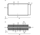
- FIG. 3(A) is a plan view of the capacitor element
- FIG. 3(B) is a side sectional view of the capacitor element
- FIG. 3(B) is a cross-sectional view taken along a plane perpendicular to the flat membrane surface and the end surface of the capacitor element.
- the capacitor element 20 includes an anode electrode 21, an inner layer CP22, and an outer layer CP23.
- a solid electrolyte layer SEL is configured by the inner layer CP22 and the outer layer CP23.
- the anode electrode 21 has a flat film shape and has an end surface 211, an end surface 212, a flat film surface 213, and a flat film surface 214. Although illustration of the detailed structure is omitted in FIG. 3, the anode electrode 21 includes a large number of holes recessed from the flat membrane surfaces 213 and 214. In other words, the portion of the anode electrode 21 having a predetermined thickness near the flat membrane surfaces 213 and 214 is a porous body in a porous state. The ratio of the thicknesses of the porous body and core metal portion on one side of the anode electrode 21 to the thickness of the porous body on the other side is approximately 1:1:1. Dielectric layer 210 covers the outer surface of anode electrode 21 .
- the dielectric layer 210 is schematically shown as covering the macroscopic surface (flat membrane surfaces 213 and 214) of the anode electrode 21. has been done. However, in reality, the dielectric layer 210 covers not only the macroscopic surface (flat membrane surfaces 213 and 214) of the anode electrode 21 but also the inner surfaces of the many holes in the anode electrode 21.
- the anode electrode 21 is made of, for example, a single metal such as aluminum, tantalum, niobium, titanium, zirconium, magnesium, or silicon, or an alloy containing these metals. Note that the anode electrode 21 is preferably made of aluminum or an aluminum alloy. The anode electrode 21 may be any valve metal body that exhibits a so-called valve action.
- the inner layer CP22 covers the surface of the dielectric layer 210.
- the inner layer CP22 is made of a conductive polymer.
- the inner layer CP22 is filled into the fine recesses of the porous portion.
- the outer layer CP23 covers the surface of the inner layer CP22.
- the outer layer CP23 is a layer formed to cover the entire dielectric layer 210 after the inner layer CP22 filling the fine recesses of the porous portion is formed.
- the outer layer CP23 is made of the same material as the inner layer CP22.
- the outer layer CP23 only needs to contain a resin material, and may be made of a different material (including composition) from the inner layer CP22.
- the insulator layer 500 is formed near the end surfaces 211 and 212 of the flat film surfaces 213 and 214 of the anode electrode 21.
- the insulator layer 500 is a frame and regulates the formation area of the inner layer CP22 and the outer layer CP23. Thereby, for example, the inner layer CP22 and the outer layer CP23 do not reach the end surface 211 of the anode electrode 21.
- the anode electrode 21 and the solid electrolyte layer face each other with the dielectric layer 210 in between, and the capacitor element 20 is a capacitor having a predetermined capacitance.
- FIG. 4 is a cross-sectional view showing the structure of the cathode film.
- the cathode film 30 includes an insulating base material 31 and a plurality of conductive fillers 32.
- the insulating base material 31 is a film with a predetermined thickness and includes a resin material.
- the conductive filler 32 is metal particles. Note that the conductive filler 32 is not limited to metal, but is preferably metal.
- the cathode film 30 has electrical conductivity while the main body has insulating properties. Further, since the cathode film 30 is not a metal foil, corrosion due to moisture or the like is suppressed.
- the insulating base material 31 of the cathode film 30 may be thermosetting or thermoplastic, each having its own advantages. Note that the advantages of each will be described later.
- the plurality of capacitor elements 20 and the plurality of cathode films 30 are arranged such that their flat film surfaces are substantially parallel to the top and bottom surfaces of the element body 11.
- the plurality of capacitor elements 20 and the plurality of cathode films 30 are alternately stacked in a direction perpendicular to the top surface and the bottom surface (height direction of the element body 11 (z-axis direction in the figure)). Note that in FIG. 2, the number of the plurality of capacitor elements 20 is three, and the number of the plurality of cathode films 30 is four, but the number is not limited to this.
- the capacitor element 20 and the cathode film 30, which are adjacent to each other in the stacking direction, are in contact with each other. More specifically, the flat film surface of the cathode film 30 contacts the outer surface 230 of the outer layer CP23 of the capacitor element 20.
- the end faces 211 of the plurality of capacitor elements 20 are exposed to the outside of the element body 11 from the end face 111 of the element body 11. Further, the end faces 311 of the plurality of cathode films 30 are exposed to the outside of the element body 11 from the end face 112 of the element body 11 .
- the resin electrode 71 contacts the end surface 111 of the element body 11 and covers the end surface 111. Thereby, the resin electrode 71 is connected to the end surfaces 211 of the plurality of capacitor elements 20.
- the external electrode 81 has a laminated structure of an electrode film 811 and an electrode film 812.
- the electrode film 811 covers the outer surface of the resin electrode 71, and the electrode film 812 covers the outer surface of the electrode film 811.
- the resin electrode 71 and the external electrode 81 constitute a first terminal conductor.
- the resin electrode 72 contacts and covers the end surface 112 of the element body 11 . Thereby, the resin electrode 72 is connected to the end surface 311 of the plurality of cathode films 30.
- the external electrode 82 has a laminated structure of an electrode film 821 and an electrode film 822.
- the electrode film 821 covers the outer surface of the resin electrode 72, and the electrode film 822 covers the outer surface of the electrode film 821.
- the resin electrode 72 and the external electrode 82 constitute a second terminal conductor.
- FIG. 5 is an enlarged cross-sectional view of the contact portion between the outer layer CP and the cathode film.
- the outer layer CP23 and the cathode film 30 coexist in the region 323 where the outer layer CP23 and the cathode film 30 are in contact.
- “mixed” means that the ratio of the resin part based on the outer layer CP23 and the resin part based on the cathode film 30 in the lamination direction (z-axis direction in FIG. 5) of the outer layer CP23 and the cathode film 30 is In the plane perpendicular to the direction (the two-dimensional region determined by the x-axis direction and the y-axis direction in FIG. 5), the area is not uniform, and the parts based on the outer layer CP23 and the parts based on the cathode film 30 are complicated. It's a mixed state. In other words, a resin solid solution region is formed.
- the contact area between the outer layer CP23 and the cathode film 30 is increased, and the adhesive strength is improved. Furthermore, the formation of a clear interface between the outer layer CP23 and the cathode film 30 due to physical property differences is suppressed, and interfacial peeling between the outer layer CP23 and the cathode film 30 is suppressed.
- the solid electrolytic capacitor 10 can suppress corrosion of the cathode and suppress peeling insulation between the cathode and the solid electrolyte layer.
- the resin material of the outer layer CP23 and the resin material of the cathode film 30 be completely the same, they may have similar compositions within the range that provides the above-mentioned effects.
- both the cathode film 30 and the resin electrode 72 contain a resin material (resin component). Thereby, the difference in physical properties between the cathode film 30 and the resin electrode 72 is reduced, and peeling and insulation between the cathode film 30 and the resin electrode 72 can be suppressed.
- FIG. 6 is a flowchart showing an example of a schematic flow of the method for manufacturing a solid electrolytic capacitor according to the present embodiment.
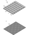
- FIG. 7(A) is an external perspective view of a capacitor element sheet
- FIG. 7(B) is an external perspective view of a cathode sheet.
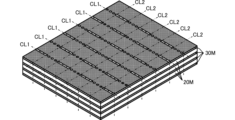
- FIG. 8 is an external perspective view of a laminate (sheet-type capacitor laminate) of a capacitor element sheet and a cathode sheet.
- a capacitor element sheet 20M is formed (S11). As shown in FIG. 7(A), the capacitor element sheet 20M is a sheet in which a plurality of capacitor elements 20 are two-dimensionally arranged.
- the specific configuration of the plurality of capacitor elements 20 is as described above, and includes an anode electrode 21, a dielectric layer 210, an inner layer CP22, and an outer layer CP23, and an insulator layer 500 for the inner layer CP22 and the outer layer CP23 is formed. has been done.
- a cathode sheet 30M is formed (S12). As shown in FIG. 7(B), the cathode sheet 30M is a sheet in which a plurality of cathode films 30 are two-dimensionally arranged. The arrangement pitch of the plurality of cathode films 30 and the arrangement pitch of the plurality of capacitor elements 20 are the same.
- a plurality of capacitor element sheets 20M and a plurality of cathode sheets 30M are sequentially laminated and heat-pressed (S13). More specifically, the plurality of capacitor element sheets 20M are stacked so that the outer surfaces 230 of the plurality of outer layers CP23 of the plurality of outer layers CP23 of the capacitor element sheets 20M adjacent to each other in the stacking direction and the cathode film 30 portion of the cathode sheet 30M face each other and come into contact with each other.
- the plurality of cathode sheets 30M are laminated. As a result, a sheet-type capacitor laminate is formed.
- this sheet-type capacitor laminate is heated and pressurized. Due to this heating and pressurization, a portion at a predetermined depth from the contact surface between the outer layer CP23 and the cathode film 30 is deformed, and as described above, the portion based on the outer layer CP23 and the portion based on the cathode film 30 become complicated. The mixture becomes mixed (resin solid solution region: see FIG. 5).
- the sheet-type capacitor laminate is cut into pieces along cutting lines CL1 and CL2 as shown in FIG. 8 (S14).
- the cathode sheet 30M cathode film 30
- burrs generated on the cut surface can be suppressed. Thereby, undesired short circuits and the like can be suppressed.
- the singulated capacitor laminate is coated with insulating resin 50 (S15).
- the insulating resin 50 is heated and pressurized.
- the insulating resin 50 is solidified, and the element body 11 of the solid electrolytic capacitor 10 is formed.
- the thermocompression bonding of the insulating resin 50 can be performed in such a way that the portion based on the above-mentioned outer layer CP23 and the portion based on the cathode film 30 are complicated. It can be used to properly adjust the mixed state.
- Terminal conductors are formed on the end faces 111 and 112 of the element body 11 (S16). More specifically, the resin electrode 71 is formed on the end surface 111 of the element body 11, and the electrode films 811 and 812 are formed on the surface of the resin electrode 71. A resin electrode 72 is formed on the end surface 112 of the element body 11, and electrode films 821 and 822 are formed on the surface of the resin electrode 72.
- the solid electrolytic capacitor 10 can be manufactured without using a conductive adhesive between the outer layer CP 23 and the cathode film 30.
- the solid electrolytic capacitor 10 in which the adhesive strength between the outer layer CP23 and the cathode film 30 is strong and peeling insulation is suppressed can be manufactured easily and more reliably.
- the insulating base material 31 is a thermosetting resin
- the shape of the cathode film 30 is highly maintainable when it is heated and compressed and cooled, that is, after the resin is solid-dissolved. This increases the stability of adhesion between the cathode film 30 and the outer layer CP23, and increases the long-term reliability of the solid electrolytic capacitor 10.
- the insulating base material 31 is a thermosetting resin and the content rate of the conductive filler 32 is high
- the shape of the cathode film 30 is highly maintained when it is heat-pressed and cooled, that is, after the resin has dissolved into solid solution. This increases the stability of adhesion between the cathode film 30 and the outer layer CP23, and increases the long-term reliability of the solid electrolytic capacitor 10.
- the content of the conductive filler 32 is high, the strength of the cathode film 30 is high, and it can be firmly bonded even in a small resin solid solution region.
- a specific numerical value indicating whether the content rate of the conductive filler 32 is low or high can be appropriately set from the viewpoint of the fluidity and strength of the cathode film 30.
- the case where the content of the conductive filler 32 is 30% by volume or less is defined as low content of the conductive filler 32, and from the viewpoint of improving the strength, the conductive filler 32 content is defined as low.
- a case where the content rate of the conductive filler 32 is 70% by volume or more is defined as having a high content rate of the conductive filler 32. Note that these are just examples, and can be adjusted as appropriate depending on the physical properties, thickness, etc. of the insulating base material 31, and the degree of influence of the content rate of the conductive filler 32 on the fluidity or strength of the cathode film 30. It can be set as appropriate.
- the insulating base material 31 is a thermoplastic resin Since the insulating base material 31 has high fluidity during heating, the resin solid solution region becomes large (in the thickness direction) and the adhesive strength between the outer layer CP23 and the cathode film 30 becomes high. Further, additional processing on the material side is not required for heating and melting.
- Solid electrolytic capacitor 11 Element body 20: Capacitor element 20M: Capacitor element sheet 21: Anode electrode 22: Inner layer CP 23: Outer layer CP 30: Cathode film 30M: Cathode sheet 31: Insulating base material 32: Conductive filler 50: Insulating resin 71, 72: Resin electrodes 81, 82: External electrodes 111, 112: End surface 210: Dielectric layer 211, 212: End surfaces 213, 214: flat film surface 230: outer surface 311: end surface 323: region 500: insulator layer 811, 812, 821, 822: electrode film
Landscapes
- Engineering & Computer Science (AREA)
- Power Engineering (AREA)
- Microelectronics & Electronic Packaging (AREA)
- Chemical & Material Sciences (AREA)
- Materials Engineering (AREA)
- Fixed Capacitors And Capacitor Manufacturing Machines (AREA)
Priority Applications (2)
| Application Number | Priority Date | Filing Date | Title |
|---|---|---|---|
| JP2024537761A JP7806906B2 (ja) | 2022-07-28 | 2023-07-25 | 固体電解コンデンサ、および、固体電解コンデンサの製造方法 |
| CN202380055385.9A CN119522463A (zh) | 2022-07-28 | 2023-07-25 | 固体电解电容器及固体电解电容器的制造方法 |
Applications Claiming Priority (2)
| Application Number | Priority Date | Filing Date | Title |
|---|---|---|---|
| JP2022-120111 | 2022-07-28 | ||
| JP2022120111 | 2022-07-28 |
Publications (1)
| Publication Number | Publication Date |
|---|---|
| WO2024024802A1 true WO2024024802A1 (ja) | 2024-02-01 |
Family
ID=89706375
Family Applications (1)
| Application Number | Title | Priority Date | Filing Date |
|---|---|---|---|
| PCT/JP2023/027262 Ceased WO2024024802A1 (ja) | 2022-07-28 | 2023-07-25 | 固体電解コンデンサ、および、固体電解コンデンサの製造方法 |
Country Status (3)
| Country | Link |
|---|---|
| JP (1) | JP7806906B2 (https=) |
| CN (1) | CN119522463A (https=) |
| WO (1) | WO2024024802A1 (https=) |
Citations (2)
| Publication number | Priority date | Publication date | Assignee | Title |
|---|---|---|---|---|
| JP2020155695A (ja) * | 2019-03-22 | 2020-09-24 | 株式会社村田製作所 | 固体電解コンデンサ |
| WO2021066090A1 (ja) * | 2019-10-04 | 2021-04-08 | 株式会社村田製作所 | 電解コンデンサ |
Family Cites Families (4)
| Publication number | Priority date | Publication date | Assignee | Title |
|---|---|---|---|---|
| JP3202668B2 (ja) * | 1997-10-21 | 2001-08-27 | 富山日本電気株式会社 | 固体電解コンデンサの製造方法 |
| JP2001148326A (ja) | 1999-11-19 | 2001-05-29 | Matsushita Electric Ind Co Ltd | タンタル固体電解コンデンサの製造方法および製造装置 |
| JP4478906B2 (ja) | 2000-03-28 | 2010-06-09 | 株式会社村田製作所 | 固体電解コンデンサ及びその製造方法 |
| JP7063301B2 (ja) | 2019-03-28 | 2022-05-09 | 株式会社村田製作所 | 固体電解コンデンサの製造方法 |
-
2023
- 2023-07-25 CN CN202380055385.9A patent/CN119522463A/zh active Pending
- 2023-07-25 WO PCT/JP2023/027262 patent/WO2024024802A1/ja not_active Ceased
- 2023-07-25 JP JP2024537761A patent/JP7806906B2/ja active Active
Patent Citations (2)
| Publication number | Priority date | Publication date | Assignee | Title |
|---|---|---|---|---|
| JP2020155695A (ja) * | 2019-03-22 | 2020-09-24 | 株式会社村田製作所 | 固体電解コンデンサ |
| WO2021066090A1 (ja) * | 2019-10-04 | 2021-04-08 | 株式会社村田製作所 | 電解コンデンサ |
Also Published As
| Publication number | Publication date |
|---|---|
| JP7806906B2 (ja) | 2026-01-27 |
| CN119522463A (zh) | 2025-02-25 |
| JPWO2024024802A1 (https=) | 2024-02-01 |
Similar Documents
| Publication | Publication Date | Title |
|---|---|---|
| JP2023053310A (ja) | 電解コンデンサおよびその製造方法 | |
| CN103959413B (zh) | 固体电解电容器及其制造方法 | |
| US10032567B2 (en) | Solid-state electrolytic capacitor manufacturing method and solid-state electrolytic capacitor | |
| JP7408288B2 (ja) | 固体電解コンデンサ | |
| JP7067512B2 (ja) | 固体電解コンデンサ | |
| JPWO2021172236A5 (https=) | ||
| TW200937469A (en) | Stacked solid electrolytic capacitor | |
| WO2022163645A1 (ja) | 電解コンデンサ | |
| CN111755253A (zh) | 固体电解电容器及固体电解电容器的制造方法 | |
| US11211204B2 (en) | Solid electrolytic capacitor and method for manufacturing same | |
| JP7806906B2 (ja) | 固体電解コンデンサ、および、固体電解コンデンサの製造方法 | |
| CN110400698A (zh) | 电子部件 | |
| JP7601054B2 (ja) | 電子部品及び電子部品の製造方法 | |
| CN223155823U (zh) | 固体电解电容器 | |
| WO2024135309A1 (ja) | 固体電解コンデンサ | |
| WO2024029458A1 (ja) | 固体電解コンデンサ | |
| JP7750381B2 (ja) | 固体電解コンデンサの製造方法 | |
| JP2023181685A (ja) | 固体電解コンデンサ | |
| WO2023243626A1 (ja) | 電解コンデンサ | |
| WO2024090047A1 (ja) | 固体電解コンデンサ | |
| WO2023153424A1 (ja) | 固体電解コンデンサ、および、固体電解コンデンサの製造方法 | |
| WO2026058571A1 (ja) | 固体電解コンデンサおよび固体電解コンデンサの製造方法 | |
| WO2025164413A1 (ja) | 固体電解コンデンサおよび固体電解コンデンサの接続素子 | |
| WO2025105152A1 (ja) | 固体電解コンデンサ、および固体電解コンデンサの製造方法 | |
| JP2025038408A (ja) | 固体電解コンデンサ |
Legal Events
| Date | Code | Title | Description |
|---|---|---|---|
| 121 | Ep: the epo has been informed by wipo that ep was designated in this application |
Ref document number: 23846532 Country of ref document: EP Kind code of ref document: A1 |
|
| WWE | Wipo information: entry into national phase |
Ref document number: 2024537761 Country of ref document: JP |
|
| WWE | Wipo information: entry into national phase |
Ref document number: 202380055385.9 Country of ref document: CN |
|
| WWP | Wipo information: published in national office |
Ref document number: 202380055385.9 Country of ref document: CN |
|
| NENP | Non-entry into the national phase |
Ref country code: DE |
|
| 122 | Ep: pct application non-entry in european phase |
Ref document number: 23846532 Country of ref document: EP Kind code of ref document: A1 |