WO2024024334A1 - バッファ回路及び撮像装置 - Google Patents
バッファ回路及び撮像装置 Download PDFInfo
- Publication number
- WO2024024334A1 WO2024024334A1 PCT/JP2023/022641 JP2023022641W WO2024024334A1 WO 2024024334 A1 WO2024024334 A1 WO 2024024334A1 JP 2023022641 W JP2023022641 W JP 2023022641W WO 2024024334 A1 WO2024024334 A1 WO 2024024334A1
- Authority
- WO
- WIPO (PCT)
- Prior art keywords
- transistor
- section
- switch section
- current source
- buffer circuit
- Prior art date
- Legal status (The legal status is an assumption and is not a legal conclusion. Google has not performed a legal analysis and makes no representation as to the accuracy of the status listed.)
- Ceased
Links
Images







Classifications
-
- H—ELECTRICITY
- H03—ELECTRONIC CIRCUITRY
- H03K—PULSE TECHNIQUE
- H03K4/00—Generating pulses having essentially a finite slope or stepped portions
- H03K4/06—Generating pulses having essentially a finite slope or stepped portions having triangular shape
- H03K4/08—Generating pulses having essentially a finite slope or stepped portions having triangular shape having sawtooth shape
- H03K4/48—Generating pulses having essentially a finite slope or stepped portions having triangular shape having sawtooth shape using as active elements semiconductor devices
-
- H—ELECTRICITY
- H03—ELECTRONIC CIRCUITRY
- H03F—AMPLIFIERS
- H03F1/00—Details of amplifiers with only discharge tubes, only semiconductor devices or only unspecified devices as amplifying elements
- H03F1/34—Negative-feedback-circuit arrangements with or without positive feedback
-
- H—ELECTRICITY
- H03—ELECTRONIC CIRCUITRY
- H03K—PULSE TECHNIQUE
- H03K19/00—Logic circuits, i.e. having at least two inputs acting on one output; Inverting circuits
- H03K19/0175—Coupling arrangements; Interface arrangements
-
- H—ELECTRICITY
- H03—ELECTRONIC CIRCUITRY
- H03K—PULSE TECHNIQUE
- H03K19/00—Logic circuits, i.e. having at least two inputs acting on one output; Inverting circuits
- H03K19/0175—Coupling arrangements; Interface arrangements
- H03K19/0185—Coupling arrangements; Interface arrangements using field effect transistors only
- H03K19/018507—Interface arrangements
-
- H—ELECTRICITY
- H03—ELECTRONIC CIRCUITRY
- H03K—PULSE TECHNIQUE
- H03K4/00—Generating pulses having essentially a finite slope or stepped portions
- H03K4/06—Generating pulses having essentially a finite slope or stepped portions having triangular shape
- H03K4/08—Generating pulses having essentially a finite slope or stepped portions having triangular shape having sawtooth shape
- H03K4/90—Linearisation of ramp; Synchronisation of pulses
-
- H—ELECTRICITY
- H04—ELECTRIC COMMUNICATION TECHNIQUE
- H04N—PICTORIAL COMMUNICATION, e.g. TELEVISION
- H04N25/00—Circuitry of solid-state image sensors [SSIS]; Control thereof
- H04N25/70—SSIS architectures; Circuits associated therewith
- H04N25/709—Circuitry for control of the power supply
-
- H—ELECTRICITY
- H04—ELECTRIC COMMUNICATION TECHNIQUE
- H04N—PICTORIAL COMMUNICATION, e.g. TELEVISION
- H04N25/00—Circuitry of solid-state image sensors [SSIS]; Control thereof
- H04N25/70—SSIS architectures; Circuits associated therewith
- H04N25/76—Addressed sensors, e.g. MOS or CMOS sensors
- H04N25/78—Readout circuits for addressed sensors, e.g. output amplifiers or A/D converters
Definitions
- the technology according to the present disclosure (present technology) relates to a buffer circuit and an imaging device including the buffer circuit.
- a pixel signal read from a pixel is typically converted from an analog signal to a digital signal by a column analog/digital converter, and subjected to signal processing by a digital signal processor (DSP).
- DSP digital signal processor
- a ramp signal source follower circuit is used in the column analog-to-digital converter.
- a buffer circuit that is advantageous for improving various characteristics is desired. Therefore, a flipped voltage follower circuit (hereinafter referred to as an FVF circuit) is known as a buffer circuit that can realize low output impedance.
- the FVF circuit can only operate within a limited voltage range, there is a problem in that the circuits that can be applied are also restricted. For example, if it can be applied to a ramp signal source follower circuit, it can be expected to lead to various improvements in characteristics, but due to the specifications of the imaging device, a ramp signal source follower circuit is required to have a wide dynamic range, so an FVF circuit is applied. I can't.
- the buffer circuit described in Patent Document 1 is a multi-stage buffer circuit using a common source amplifier circuit. Therefore, the configuration is complicated, the circuit area becomes large, and the power consumption also increases.
- the present disclosure has been made in view of the above circumstances, and provides a buffer circuit and an imaging device that can realize a wide dynamic range while maintaining low output impedance, and can reduce area and power consumption.
- the purpose is to
- One aspect of the present disclosure includes a first transistor having a gate into which an input signal is input, a current source connected to one terminal of the first transistor, and a current source connected to the other terminal of the first transistor.
- a second transistor provided between the current source and the gate of the second transistor; an output terminal connected to one or the other terminal of the first transistor; and first and second transistors provided between the current source and the gate of the second transistor.
- a capacitor, a first feedback circuit is formed by the first transistor, the second transistor, and the first capacitor, and a first feedback circuit is formed by the first transistor, the current source, and the second capacitor.
- a second feedback circuit is formed by the buffer circuit.
- aspects of the present disclosure include a pixel array section and a buffer circuit configured of a plurality of pixels capable of generating pixel signals according to light incident from the outside, and an output signal of the buffer circuit and each of the plurality of pixels.
- a signal processing unit that compares the pixel signals output from the unit and generates image data based on the comparison result, and supplies power necessary for the operation of each of the pixel array unit, the buffer circuit, and the signal processing unit.
- an imaging device comprising: a power supply circuit; the buffer circuit includes a first transistor having a gate to which an input signal is input; a current source connected to one terminal of the first transistor; and a current source connected to one terminal of the first transistor; a second transistor connected to the other terminal of the first transistor; an output terminal connected to one or the other terminal of the first transistor; and a connection between the current source and the gate of the second transistor.
- a first feedback circuit is formed by the first transistor, the second transistor, and the first capacitor;
- a second feedback circuit is formed by the current source and the second capacitor.
- FIG. 1 is a block diagram illustrating an example of a schematic configuration of an imaging device according to a first embodiment of the present disclosure.
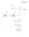
- FIG. 2 is a block diagram for explaining an example of an image signal readout mechanism in the imaging device according to the first embodiment of the present disclosure.
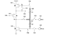
- FIG. 1 is a circuit diagram (part 1) showing the configuration of a ramp signal buffer circuit according to a first embodiment of the present disclosure.
- FIG. 2 is a circuit diagram (Part 2) showing the configuration of the ramp signal buffer circuit according to the first embodiment of the present disclosure.
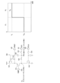
- FIG. 6 is a diagram showing a change in voltage Vfb between the first capacitor and the second capacitor in a case where a second feedback circuit is not formed.
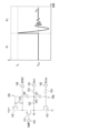
- FIG. 7 is a diagram showing a change in voltage Vfb between the first capacitor and the second capacitor when a second feedback circuit is formed.
- FIG. 2 is a circuit diagram showing the configuration of a ramp signal buffer circuit according to a second embodiment of the present disclosure.
- FIG. 7 is a circuit diagram showing the configuration of a power supply circuit and a ramp signal buffer circuit according to a third embodiment of the present disclosure.
- FIG. 7 is a circuit diagram showing the configuration of a ramp signal buffer circuit according to a fourth embodiment of the present disclosure.
- FIG. 7 is a circuit diagram showing the configuration of a ramp signal buffer circuit according to a fifth embodiment of the present disclosure.
- FIG. 7 is a circuit diagram showing the configuration of a ramp signal buffer circuit according to a sixth embodiment of the present disclosure.
- FIG. 1 is a diagram showing a change in voltage Vfb between the first capacitor and the second capacitor when a second feedback circuit is formed.
- FIG. 2 is a circuit diagram showing the configuration of a ramp signal buffer circuit according to a second
- FIG. 7 is a circuit diagram showing the configuration of a ramp signal buffer circuit according to a seventh embodiment of the present disclosure.
- FIG. 7 is a circuit diagram showing the configuration of a ramp signal buffer circuit according to an eighth embodiment of the present disclosure.
- 1 is a block diagram showing a configuration example of an imaging system as an electronic device to which the present technology is applied.
- FIG. 1 is a block diagram illustrating an example of a schematic configuration of an imaging device according to a first embodiment of the present disclosure.
- the imaging device 1 uses a photoelectric conversion element such as a photodiode constituting each pixel to convert the amount of charge corresponding to the intensity of light imaged onto the pixel into an electrical signal, and outputs this as image data.
- It is a semiconductor device, and is configured as, for example, a CMOS image sensor.
- the imaging device 1 may be configured integrally as a system-on-chip (SoC) such as a CMOS LSI, but for example, some of the components described below may be configured as separate LSIs.
- SoC system-on-chip
- the imaging device 1 includes, for example, a pixel array section 11, a vertical drive section 12, a column processing section 13, a horizontal drive section 14, a system control section 15, a signal processing section 16, It is configured to include components such as a data storage section 17.
- the pixel array section 11 includes a group of photoelectric conversion elements such as photodiodes that constitute the pixels 110 arranged in an array in the horizontal direction (row direction) and the vertical direction (column direction).
- the pixel array section 11 converts the amount of charge corresponding to the intensity of the incident light imaged onto each pixel 110 into an electrical signal, and outputs it as a pixel signal.
- the vertical drive section 12 includes a shift register, an address decoder, etc.
- the vertical drive section 12 drives each pixel 110 of the pixel array section 11, for example, simultaneously or in row units by supplying drive signals and the like to each pixel 110 via a plurality of pixel drive lines 18.
- the column processing section 13 reads out pixel signals from each pixel via the vertical signal line (VSL) 19 for each pixel row (column) of the pixel array section 11, and performs noise removal processing, correlated double sampling (CDS) processing, and A/D (Analog-to-Digital) conversion processing.
- the pixel signals processed by the column processing section 13 are output to the signal processing section 16.
- the horizontal drive section 14 includes a shift register, an address decoder, etc.
- the horizontal drive unit 14 sequentially selects pixels 110 corresponding to the pixel columns of the column processing unit 13. By this selective scanning by the horizontal driving section 14, pixel signals subjected to signal processing for each pixel 110 in the column processing section 13 are sequentially output to the signal processing section 16.
- the system control unit 15 includes a timing generator and the like that generate various timing signals.
- the system control unit 15 controls the vertical drive unit 12, the column processing unit 13, and the horizontal drive unit 14 based on a timing signal generated by a timing generator (not shown), for example.
- the signal processing unit 16 performs signal processing such as arithmetic processing on the pixel signals supplied from the column processing unit 13 while temporarily storing data in the data storage unit 17 as necessary, and adds data to each pixel signal. Outputs an image signal based on the
- the imaging device 1 to which the present technology is applied is not limited to the configuration described above.
- the data storage section 17 is arranged after the column processing section 13, and pixel signals output from the column processing section 13 are supplied to the signal processing section 16 via the data storage section 17. It may be configured as follows. Alternatively, the imaging device 1 may be configured such that the column processing section 13, data storage section 17, and signal processing section 16 connected in series process each pixel signal in parallel.
- FIG. 2 is a block diagram for explaining an example of an image signal readout mechanism in the imaging device according to the first embodiment of the present disclosure.
- a pixel signal readout mechanism 20 from one pixel 110 in one pixel column is exemplarily shown.
- a ramp signal buffer circuit 131, a ramp signal generation circuit 132, and an analog/digital converter (hereinafter referred to as an AD converter) 133 are shown as the configuration of the column processing section 13.
- the ramp signal generation circuit 132 generates and outputs a ramp signal necessary for AD conversion processing by the AD converter 133.
- a ramp signal is, for example, a signal whose voltage level changes in slope over time.
- the ramp signal buffer circuit 131 performs impedance conversion processing on the ramp signal output from the ramp signal generation circuit 132.
- the AD converter 133 converts the analog pixel signal output from the pixel 110 into a digital pixel signal (pixel data).
- the AD converter 133 is provided in parallel for each vertical signal line 19 corresponding to a pixel column.
- the AD converter 133 includes a comparator 134 and a counter 135. That is, the AD converter 133 performs counting using the counter 135 while comparing the ramp signal outputted from the ramp signal buffer circuit 131 and the pixel signal read from the pixel 110 over time using the comparator 134. The obtained value is output to the signal processing section 16 as a digital pixel signal.
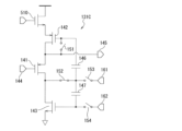
- FIG. 3 and 4 are circuit diagrams showing the configuration of the ramp signal buffer circuit 131 according to the first embodiment of the present disclosure.
- FIG. 3 is a circuit diagram showing the configuration of the ramp signal buffer circuit 131 in the reset mode
- FIG. 4 is a circuit diagram showing the configuration of the ramp signal buffer circuit 131 in the normal drive mode (AD mode). .
- the ramp signal buffer circuit 131 includes an input control section 141, an output control section 142, a current source 143, an input terminal 144, an output terminal 145, and a first capacitor (C1) 146. , the second capacitor (C2) 147, the first switch section 151, the second switch section 152, the third switch section 153, the fourth switch section 154, and the first voltage application section 161. and a second voltage application section 162.
- the input control section 141, the output control section 142, and the current source 143 are configured of, for example, P-type metal-oxide-semiconductor (MOS) transistors.
- the input terminal 144 is connected to the gate of a MOS transistor that constitutes the input control section 141.
- the input terminal 144 inputs the ramp signal output from the ramp signal generation circuit 132 to the gate of the input control section 141 .
- the input control section 141 When the voltage of the ramp signal is equal to or higher than the threshold voltage Vth1 between the gate and drain of the MOS transistor constituting the input control section 141, the input control section 141 is in a conductive state (on state).
- the input control section 141 becomes non-conductive (off state).
- the source of the input control section 141 is connected to the drain of a MOS transistor constituting the output control section 142 and the output terminal 145. Furthermore, the drain of the input control section 141 is connected to the drain of a MOS transistor that constitutes the current source 143 .
- the input control unit 141 inputs the ramp signal output from the ramp signal generation circuit 132 to the AD converter 133 by establishing continuity between the input terminal 144 and the output terminal 145.
- a first capacitor 146 and a second capacitor 147 are connected in series between the gate of the output control section 142 and the gate of the current source 143.
- the input control section 141, the output control section 142, and the first capacitor 146 form a first feedback circuit FB1.
- the input control section 141, the current source 143, and the second capacitor 147 form a second feedback circuit FB2.
- a power source is connected to the source of the output control unit 142.
- the lamp signal input to the input terminal 144 is input to the gate of the output control unit 142 as an alternating current (AC) voltage of the lamp signal via the drain of the input control unit 141 and the first capacitor 146.
- the output control section 142 amplifies the output current flowing to the output terminal 145.
- the first switch section 151 turns on/off the connection between the gate of the output control section 142 and the output terminal 145.
- the second switch section 152 turns on/off the connection between the drain of the input control section 141 and the first capacitor 146 and the second capacitor 147.
- the third switch section 153 turns on/off the connection of the first voltage application section 161 to the first feedback circuit FB1.
- the fourth switch section 154 turns on/off the connection of the second voltage application section 162 to the second feedback circuit FB2.
- the first switch section 151, the third switch section 153, and the fourth switch section 154 are turned on, and the second switch section 152 is turned off. That is, by turning on the first switch section 151, the output control section 142 is diode-connected, and the gate of the output control section 142 is charged with the voltage Vy.
- the third switch section 153 the voltage Vfb between the first capacitor 146 and the second capacitor 147 is charged to the externally applied voltage Vext from the first voltage applying section 161.
- the fourth switch section 154 the voltage Vz applied to the gate of the current source 143 is charged to the externally applied voltage Vbias from the second voltage application section 162.
- the first switch section 151, the third switch section 153, and the fourth switch section 154 are turned off, and the second switch section 152 is turned on. That is, by turning on the second switch section 152, a signal is fed back from the drain of the input control section 141 to the gate of the output control section 142, and Vx and Vext are fed back from the drain of the input control section 141 to the gate of the current source 143. Feedback the difference.
- the input dynamic range Vin is as follows. Vx-
- Vsg1 is a voltage between the gate and source of the MOS transistor that constitutes the input control section 141.
- the drain voltage Vx of the input control section 141 can be determined by the externally applied voltage Vext. Moreover, the error in the gate voltage Vz of the current source 143 caused by this becomes minute.
- FIG. 5 shows changes in the voltage Vfb between the first capacitor 146 and the second capacitor 147 when the second feedback circuit FB2 is not formed.
- FIG. 6 shows changes in the voltage Vfb between the first capacitor 146 and the second capacitor 147 when the second feedback circuit FB2 is formed.
- the first capacitor 146 is inserted into the first feedback circuit FB1
- the second capacitor 147 is inserted into the second feedback circuit FB2
- only AC voltage is output.
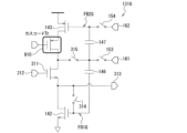
- FIG. 7 is a circuit diagram showing the configuration of a ramp signal buffer circuit 131A according to the second embodiment of the present disclosure.
- the same parts as those in FIGS. 3 and 4 are given the same reference numerals, and detailed description thereof will be omitted.
- the input control section 311 is composed of, for example, an N-type MOS transistor with a polarity opposite to that of the P-type.
- the input terminal 312 is connected to the gate of a MOS transistor that constitutes the input control section 311.
- the input control section 311 becomes conductive (on state).
- the input control section 311 becomes non-conductive (off state).
- the drain of the input control section 311 is connected to the drain of a MOS transistor that constitutes the current source 143. Furthermore, the source of the input control section 311 is connected to the drain of a MOS transistor constituting the output control section 142 and the output terminal 313 .
- the input control section 311, current source 143, and second capacitor 147 form a second feedback circuit FB2A.
- the input control section 311, the output control section 142, and the first capacitor 146 form a first feedback circuit FB1A.
- the first switch section 314 turns on/off the connection between the gate of the output control section 142 and the output terminal 313.
- the second switch section 315 turns on/off the connection between the drain of the input control section 311 and the first capacitor 146 and the second capacitor 147.
- the first switch section 314, the third switch section 153, and the fourth switch section 154 are turned on, and the second switch section 315 is turned off. That is, by turning on the first switch section 314, the output control section 142 is diode-connected, and the gate of the output control section 142 is charged with the voltage Vy.
- the third switch section 153 the voltage Vfb between the first capacitor 146 and the second capacitor 147 is charged to the externally applied voltage Vext from the first voltage applying section 161.
- the fourth switch section 154 the voltage Vz applied to the gate of the current source 143 is charged to the externally applied voltage Vbias from the second voltage application section 162.
- the first switch section 314, the third switch section 153, and the fourth switch section 154 are turned off, and the second switch section 315 is turned on. That is, by turning on the second switch section 315, a signal is fed back from the drain of the input control section 311 to the gate of the current source 143, and Vy and Vext are transferred from the drain of the input control section 311 to the gate of the output control section 142. Feedback the difference.
- FIG. 8 is a circuit diagram showing the configuration of a power supply circuit 410 and a ramp signal buffer circuit 131B according to a third embodiment of the present disclosure.
- the same parts as those in FIGS. 3 and 4 are given the same reference numerals, and detailed description thereof will be omitted.
- the power supply circuit 410 supplies power necessary for each operation of the pixel array section 11, the column processing section 13 including the ramp signal buffer circuit 131B, and the signal processing section 16.
- a power supply circuit 410 according to the fourth embodiment of the present disclosure includes an LDO (Low Drop Out) 411.
- the LDO 411 is a DC (direct current)-DC (direct current) converter.
- the LDO 411 is a component that compensates for the power supply rejection ratio (PSRR) of the power supply circuit 410.
- the power supply voltage fluctuation rejection ratio of the power supply circuit 410 is the ability of the power supply circuit 410 to eliminate voltage fluctuations in the power supply VDD when there is fluctuation (ripple) in the power supply voltage.
- the LDO 411 can attenuate the amount of variation in the power supply voltage input from the power supply circuit 410 and output a reference signal at a constant voltage level to the input control section 141, output control section 142, and current source 143.
- FIG. 9 is a circuit diagram showing the configuration of a ramp signal buffer circuit 131C according to the fourth embodiment of the present disclosure.
- the same parts as those in FIGS. 3 and 4 are given the same reference numerals, and detailed description thereof will be omitted.
- a ramp signal buffer circuit 131C includes a source follower circuit 510 connected to a power supply line that supplies power necessary for operation to an input control section 141, an output control section 142, and a current source 143. Equipped with.
- the source follower circuit 510 is composed of, for example, an N-type MOS transistor.
- the source of the output control section 142 is connected to the source of the source follower circuit 510 .
- a power supply line is connected to the drain of the source follower circuit 510.
- the source follower circuit 510 can attenuate power supply noise of the power supply voltage input through the drain and output a reference signal at a constant voltage level to the input control section 141, output control section 142, and current source 143.
- FIG. 10 is a circuit diagram showing the configuration of a ramp signal buffer circuit 131D according to the fifth embodiment of the present disclosure.
- the same parts as those in FIGS. 3 and 4 are given the same reference numerals and detailed explanations will be omitted.
- a ramp signal buffer circuit 131D has a cascode transistor 610 inserted in a first feedback circuit FB1D formed by an input control section 141, an output control section 142, and a first capacitor 146.
- Cascode transistor 610 is composed of, for example, a P-type MOS transistor.
- the source of the input control section 141 is connected to the drain of the cascode transistor 610.
- the source of the cascode transistor 610 is connected to the drain of the output control section 142 and the output terminal 145.
- FIG. 11 is a circuit diagram showing the configuration of a ramp signal buffer circuit 131E according to the sixth embodiment of the present disclosure.
- the same parts as those in FIG. 7 are given the same reference numerals and detailed explanations will be omitted.
- a ramp signal buffer circuit 131E has a cascode transistor 710 inserted in a first feedback circuit FB1E formed by an input control section 311, an output control section 142, and a first capacitor 146. .
- the cascode transistor 710 is composed of, for example, an N-type MOS transistor.
- the source of the input control section 141 is connected to the drain of the cascode transistor 710.
- the source of the cascode transistor 710 is connected to the drain of the output control section 142 and the output terminal 313.
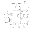
- FIG. 12 is a circuit diagram showing the configuration of a ramp signal buffer circuit 131F according to the seventh embodiment of the present disclosure.
- the same parts as those in FIGS. 3 and 4 are given the same reference numerals and detailed explanations will be omitted.
- a ramp signal buffer circuit 131F has a cascode transistor 810 inserted into a second feedback circuit FB2F formed by an input control section 141, a current source 143, and a second capacitor 147.
- Cascode transistor 810 is composed of, for example, an N-type MOS transistor, and is a component for compensating the linearity of current source 143.
- the drain of the input control section 141 is connected to the drain of the cascode transistor 810.
- the source of cascode transistor 810 is connected to the drain of current source 143 .
- FIG. 13 is a circuit diagram showing the configuration of a ramp signal buffer circuit 131G according to the eighth embodiment of the present disclosure.
- the same parts as those in FIG. 7 are given the same reference numerals and detailed explanations will be omitted.
- a ramp signal buffer circuit 131G has a cascode transistor 910 inserted into a second feedback circuit FB2G formed by an input control section 311, a current source 143, and a second capacitor 147.
- Cascode transistor 910 is composed of, for example, a P-type MOS transistor, and is a component for compensating the linearity of current source 143.
- the drain of the input control section 311 is connected to the drain of the cascode transistor 910.
- the drain of current source 143 is connected to the source of cascode transistor 910.
- FIG. 14 is a block diagram showing a configuration example of an imaging system as an electronic device to which the present technology is applied.
- An imaging system 2201 shown in FIG. 14 includes an optical system 2202, a shutter device 2203, a solid-state image sensor 2204 as an imaging device, a control circuit 2205, a signal processing circuit 2206, a monitor 2207, and two memories 2208, and is stationary. It is possible to capture images and moving images.
- the optical system 2202 includes one or more lenses, guides light (incident light) from a subject to the solid-state image sensor 2204, and forms an image on the light-receiving surface of the solid-state image sensor 2204.
- the shutter device 2203 is disposed between the optical system 2202 and the solid-state image sensor 2204, and controls the light irradiation period and the light shielding period to the solid-state image sensor 2204 under the control of the control circuit 2205.
- the solid-state image sensor 2204 is configured by a package containing the above-described solid-state image sensor.
- the solid-state image sensor 2204 accumulates signal charges for a certain period of time according to the light that is imaged on the light receiving surface via the optical system 2202 and the shutter device 2203.
- the signal charge accumulated in the solid-state image sensor 2204 is transferred according to a drive signal (timing signal) supplied from the control circuit 2205.
- the control circuit 2205 outputs a drive signal that controls the transfer operation of the solid-state image sensor 2204 and the shutter operation of the shutter device 2203, and drives the solid-state image sensor 2204 and the shutter device 2203.
- the signal processing circuit 2206 performs various signal processing on the signal charges output from the solid-state image sensor 2204.
- An image (image data) obtained by signal processing by the signal processing circuit 2206 is supplied to a monitor 2207 and displayed, or supplied to a memory 2208 and stored (recorded). Also in the imaging system 2201 configured in this way, the imaging device 1 can be applied instead of the solid-state imaging device 2204 described above.
- the present disclosure can also have the following configuration.
- a first transistor having a gate into which an input signal is input; a current source connected to one terminal of the first transistor; a second transistor connected to the other terminal of the first transistor; an output terminal connected to one or the other terminal of the first transistor; first and second capacitors provided between the current source and the gate of the second transistor, A first feedback circuit is formed by the first transistor, the second transistor, and the first capacitor, a second feedback circuit is formed by the first transistor, the current source, and the second capacitor; buffer circuit.
- the buffer circuit according to (2) above further comprising a second voltage application section that applies a second voltage different from the first voltage to the second feedback circuit.
- a first switch section that turns on and off a connection between the gate of the second transistor and the output terminal; a second switch unit that turns on and off connections between a terminal to which the output terminal of the first transistor is not connected and the first and second capacitors; a third switch unit that turns on and off the connection between the first voltage application unit and the first and second capacitors; a fourth switch unit that turns on and off connections between the second voltage application unit, the second capacitor, and the current source; in reset mode, turning on the first switch section, the third switch section, and the fourth switch section, and turning off the second switch section;
- the buffer circuit according to (3) above wherein the first switch section, the third switch section, and the fourth switch section are turned off and the second switch section is turned on in the drive mode.
- the first transistor is of a first conductivity type
- (6) a first voltage application section that applies a predetermined first voltage to the first feedback circuit; a second voltage application unit that applies a second voltage different from the first voltage to the second feedback circuit; a first switch section that turns on and off a connection between the gate of the second transistor and the output terminal; a second switch unit that turns on and off connections between a terminal to which the output terminal of the first transistor is not connected and the first and second capacitors; a third switch unit that turns on and off the connection between the first voltage application unit and the first and second capacitors; a fourth switch unit that turns on and off connections between the second voltage application unit, the second capacitor, and the current source; in reset mode, turning on the first switch section, the third switch section, and the fourth switch section, and turning off the second switch section;
- a first voltage application section that applies a predetermined first voltage to the first feedback circuit; a second voltage application unit that applies a second voltage different from the first voltage to the second feedback circuit; a first switch section that turns on and off a connection between the second transistor and the output terminal; a second switch unit that turns on and off connections between a terminal to which the output terminal of the first transistor is not connected and the first and second capacitors; a third switch unit that turns on and off the connection between the first voltage application unit and the first and second capacitors; a fourth switch unit that turns on and off connections between the second voltage application unit, the second capacitor, and the current source; in reset mode, turning on the first switch section, the third switch section, and the fourth switch section, and turning off the second switch section;
- the buffer circuit according to (9) above, wherein the first switch section, the third switch section, and the fourth switch section are turned off and the second switch section is turned on in the drive mode.
- a pixel array section composed of a plurality of pixels capable of generating pixel signals according to light incident from the outside; a buffer circuit; a signal processing unit that compares the output signal of the buffer circuit with a pixel signal output from each of the plurality of pixels and generates image data based on the comparison result;
- An imaging device comprising: a power supply circuit that supplies power necessary for the operation of each of the pixel array section, the buffer circuit, and the signal processing section,
- the buffer circuit is a first transistor having a gate into which an input signal is input; a current source connected to one terminal of the first transistor; a second transistor connected to the other terminal of the first transistor; an output terminal connected to one or the other terminal of the first transistor; first and second capacitors provided between the current source and the gate of the second transistor,
- a first feedback circuit is formed by the first transistor, the second transistor, and the first capacitor, a second feedback circuit is formed by the first transistor, the current source, and the second capacitor;
- Imaging device (15) The imaging device according to (14),
- Imaging device 11 Pixel array section 12 Vertical drive section 13 Column processing section 14 Horizontal drive section 15 System control section 16 Signal processing section 17 Data storage section 18 Pixel drive line 19 Vertical signal line 20 Pixel signal readout mechanism 110 Pixels 131, 131A, 131B, 131C, 131D, 131E, 131G Ramp signal buffer circuit 132 Ramp signal generation circuit 133 AD converter 134 Comparator 135 Counter 141, 311 Input control section 142 Output control section 143 Current source 144, 312 Input terminal 145, 313 Output terminal 146 First capacitor (C1) 147 Second capacitor (C2) 151, 314 First switch section 152, 315 Second switch section 153 Third switch section 154 Fourth switch section 161 First voltage application section 162 Second voltage application section 201 First module 202 Second Modules 211, 212 Source follower circuit 410 Power supply circuit 411 LDO 510 Source follower circuit 610, 710, 810, 910 Cascode transistor 2201 Imaging system 2202 Optical system 2203 Shutter device 2204 Solid-state image sensor
Landscapes
- Engineering & Computer Science (AREA)
- Computer Hardware Design (AREA)
- Multimedia (AREA)
- Signal Processing (AREA)
- Physics & Mathematics (AREA)
- Computing Systems (AREA)
- General Engineering & Computer Science (AREA)
- Mathematical Physics (AREA)
- Power Engineering (AREA)
- Transforming Light Signals Into Electric Signals (AREA)
Abstract
Description
(撮像装置の全体構成)
図1は、本開示の第1の実施形態に係る撮像装置の概略的構成の一例を示すブロック図である。撮像装置1は、各画素を構成するフォトダイオード等の光電変換素子を用いて、該画素上に結像した光の強弱に応じた電荷量を電気信号に変換し、これを画像データとして出力する半導体装置であり、例えばCMOSイメージセンサとして構成される。撮像装置1は、例えば、CMOS LSIのようなシステム・オン・チップ(SoC)として一体的に構成され得るが、例えば、以下に示すいくつかのコンポーネントが別体のLSIとして構成されても良い。
同図では、カラム処理部13の構成として、ランプ信号バッファ回路131と、ランプ信号生成回路132と、アナログ/デジタル変換器(以下、AD変換器と称する)133とが示されている。
図3及び図4は、本開示の第1の実施形態に係るランプ信号バッファ回路131の構成を示す回路図である。図3は、リセットモードのときのランプ信号バッファ回路131の構成を示す回路図であり、図4は、通常駆動モード(ADモード)のときのランプ信号バッファ回路131の構成を示す回路図である。
Vx-|Vth1|<Vin<Vy+|Vth2|-Vsg1
ここで、電流源143へのフィードバックが必要な理由について説明する。
リセットモードΦ1のときに、第1のキャパシタ146及び第2のキャパシタ147に蓄積される電荷をQ1,Q2、駆動モードΦ2のときに、第1のキャパシタ146及び第2のキャパシタ147に蓄積された電荷をQ’1,Q’2とする。Q1,Q2とQ’1,Q’2で電荷保存則が成り立つと仮定すると(実際はVxからわずかに電荷が抜けるための誤差が生じる)、次式が成り立つ。
Q1+Q2=Q’1+Q’2
C1(Vext-Vy)+C2(Vext-Vbias)=C1(Vx-Vy)+C2(Vx-Vz)
Vz=Vbias+K(Vx-Vext)
K=(C1+C2)/C2
負帰還をかけることにより、入力制御部141のドレイン電圧Vxを外部の印加電圧Vextによって決めることができる。また、これによって生じる電流源143のゲート電圧Vzの誤差は微小となる。
図5は、第2のフィードバック回路FB2を形成しない場合における第1のキャパシタ146と第2のキャパシタ147との間の電圧Vfbの変化を示している。
以上のように第1の実施形態によれば、第1のフィードバック回路FB1に第1のキャパシタ146を挿入し、第2のフィードバック回路FB2に第2のキャパシタ147を挿入して交流電圧のみを出力制御部142のゲートに帰還することで低出力インピーダンスを維持しつつ、入力制御部141のドレインと出力制御部142のゲートが直流的に同電位となることを避けることができ、広いダイナミックレンジを確保できる。
図7は、本開示の第2の実施形態に係るランプ信号バッファ回路131Aの構成を示す回路図である。図7において、上記図3及び図4と同一部分には同一符号を付して詳細な説明を省略する。
以上のように第2の実施形態によれば、上記第1の実施形態と同様の作用効果が得られる。
図8は、本開示の第3の実施形態に係る電源回路410及びランプ信号バッファ回路131Bの構成を示す回路図である。図8において、上記図3及び図4と同一部分には同一符号を付して詳細な説明を省略する。
以上のように第3の実施形態によれば、電源回路410自体にLDO411を備えることで、電源電圧変動除去比の改善を図ることができる。
図9は、本開示の第4の実施形態に係るランプ信号バッファ回路131Cの構成を示す回路図である。図9において、上記図3及び図4と同一部分には同一符号を付して詳細な説明を省略する。
以上のように第4の実施形態によれば、ソースフォロワ回路510を備えることにより、電源ノイズを減衰させることができる。
図10は、本開示の第5の実施形態に係るランプ信号バッファ回路131Dの構成を示す回路図である。図10において、上記図3及び図4と同一部分には同一符号を付して詳細な説明を省略する。
以上のように第5の実施形態によれば、第1のフィードバック回路FB1Dにカスコードトランジスタ610を挿入することにより、第1のフィードバック回路FB1Dのループゲインの向上を図ることができる。
図11は、本開示の第6の実施形態に係るランプ信号バッファ回路131Eの構成を示す回路図である。図11において、上記図7と同一部分には同一符号を付して詳細な説明を省略する。
以上のように第6の実施形態によれば、第1のフィードバック回路FB1Eにカスコードトランジスタ710を挿入することにより、第1のフィードバック回路FB1Eのループゲインの向上を図ることができる。
図12は、本開示の第7の実施形態に係るランプ信号バッファ回路131Fの構成を示す回路図である。図12において、上記図3及び図4と同一部分には同一符号を付して詳細な説明を省略する。
以上のように第7の実施形態によれば、入力制御部141と電流源143との間に、カスコードトランジスタ810を接続することで、電流源143の線形性向上を図ることができる。
図13は、本開示の第8の実施形態に係るランプ信号バッファ回路131Gの構成を示す回路図である。図13において、上記図7と同一部分には同一符号を付して詳細な説明を省略する。
以上のように第8の実施形態によれば、入力制御部311と電流源143との間に、カスコードトランジスタ910を接続することで、電流源143の線形性向上を図ることができる。
上記のように、本技術は第1から第8の実施形態によって記載したが、この開示の一部をなす論述及び図面は本技術を限定するものであると理解すべきではない。上記の第1から第8の実施形態が開示する技術内容の趣旨を理解すれば、当業者には様々な代替実施形態、実施例及び運用技術が本技術に含まれ得ることが明らかとなろう。また、第1から第8の実施形態がそれぞれ開示する構成を、矛盾の生じない範囲で適宜組み合わせることができる。例えば、複数の異なる実施形態がそれぞれ開示する構成を組み合わせてもよく、同一の実施形態の複数の異なる変形例がそれぞれ開示する構成を組み合わせてもよい。
上述した光検出装置は、例えば、デジタルスチルカメラやデジタルビデオカメラなどの撮像装置、撮像機能を備えた携帯電話機、または、撮像機能を備えた他の機器といった各種の電子機器に適用することができる。
図14は、本技術を適用した電子機器としての撮像システムの構成例を示すブロック図である。
シャッタ装置2203は、光学系2202および固体撮像素子2204の間に配置され、制御回路2205の制御に従って、固体撮像素子2204への光照射期間および遮光期間を制御する。
このように構成されている撮像システム2201においても、上述した固体撮像素子2204に代えて、撮像装置1を適用することが可能となる。
(1)
入力信号が入力されるゲートを有する第1のトランジスタと、
前記第1のトランジスタの一方の端子に接続される電流源と、
前記第1のトランジスタの他方の端子に接続される第2のトランジスタと、
前記第1のトランジスタの一方または他方の端子に接続される出力端子と、
前記電流源と前記第2のトランジスタのゲートとの間に設けられる第1及び第2のキャパシタと、を備え、
前記第1のトランジスタと前記第2のトランジスタと前記第1のキャパシタとによって第1のフィードバック回路が形成され、
前記第1のトランジスタと前記電流源と前記第2のキャパシタとによって第2のフィードバック回路が形成される、
バッファ回路。
(2)
前記第1のフィードバック回路に対し、所定の第1の電圧を印加する第1の電圧印加部をさらに備える、上記(1)に記載のバッファ回路。
(3)
前記第2のフィードバック回路に対し、前記第1の電圧とは異なる第2の電圧を印加する第2の電圧印加部をさらに備える、上記(2)に記載のバッファ回路。
(4)
前記第2のトランジスタのゲートと前記出力端子との接続をオン・オフする第1のスイッチ部と、
前記第1のトランジスタの前記出力端子が接続されない端子と前記第1及び第2のキャパシタとの接続をオン・オフする第2のスイッチ部と、
前記第1の電圧印加部と前記第1及び第2のキャパシタの接続をオン・オフする第3のスイッチ部と、
前記第2の電圧印加部と前記第2のキャパシタ及び前記電流源との接続をオン・オフする第4のスイッチ部と、を備え、
リセットモードで、前記第1のスイッチ部、前記第3のスイッチ部、前記第4のスイッチ部をオンし、前記第2のスイッチ部をオフし、
駆動モードで、前記第1のスイッチ部、前記第3のスイッチ部、前記第4のスイッチ部をオフし、前記第2のスイッチ部をオンする、上記(3)に記載のバッファ回路。
(5)
前記第1のトランジスタは、第1の導電型であり、
前記出力端子は、前記第1のトランジスタと前記第2のトランジスタとの間に接続される、上記(1)に記載のバッファ回路。
(6)
前記第1のフィードバック回路に対し、所定の第1の電圧を印加する第1の電圧印加部と、
前記第2のフィードバック回路に対し、前記第1の電圧とは異なる第2の電圧を印加する第2の電圧印加部と、
前記第2のトランジスタのゲートと前記出力端子との接続をオン・オフする第1のスイッチ部と、
前記第1のトランジスタの前記出力端子が接続されない端子と前記第1及び第2のキャパシタとの接続をオン・オフする第2のスイッチ部と、
前記第1の電圧印加部と前記第1及び第2のキャパシタの接続をオン・オフする第3のスイッチ部と、
前記第2の電圧印加部と前記第2のキャパシタ及び前記電流源との接続をオン・オフする第4のスイッチ部と、を備え、
リセットモードで、前記第1のスイッチ部、前記第3のスイッチ部、前記第4のスイッチ部をオンし、前記第2のスイッチ部をオフし、
駆動モードで、前記第1のスイッチ部、前記第3のスイッチ部、前記第4のスイッチ部をオフし、前記第2のスイッチ部をオンする、上記(5)に記載のバッファ回路。
(7)
前記第1のトランジスタと前記出力端子との間に、カスコードトランジスタを接続する、上記(5)に記載のバッファ回路。
(8)
前記第1のトランジスタと前記電流源との間に、カスコードトランジスタを接続する、上記(5)に記載のバッファ回路。
(9)
前記第1のトランジスタは、前記第1の導電型とは逆極性の第2の導電型であり、
前記出力端子は、前記第1のトランジスタと前記第2のトランジスタとの間に接続される、上記(5)に記載のバッファ回路。
(10)
前記第1のフィードバック回路に対し、所定の第1の電圧を印加する第1の電圧印加部と、
前記第2のフィードバック回路に対し、前記第1の電圧とは異なる第2の電圧を印加する第2の電圧印加部と、
前記第2のトランジスタと前記出力端子との接続をオン・オフする第1のスイッチ部と、
前記第1のトランジスタの前記出力端子が接続されない端子と前記第1及び第2のキャパシタとの接続をオン・オフする第2のスイッチ部と、
前記第1の電圧印加部と前記第1及び第2のキャパシタの接続をオン・オフする第3のスイッチ部と、
前記第2の電圧印加部と前記第2のキャパシタ及び前記電流源との接続をオン・オフする第4のスイッチ部と、を備え、
リセットモードで、前記第1のスイッチ部、前記第3のスイッチ部、前記第4のスイッチ部をオンし、前記第2のスイッチ部をオフし、
駆動モードで、前記第1のスイッチ部、前記第3のスイッチ部、前記第4のスイッチ部をオフし、前記第2のスイッチ部をオンする、上記(9)に記載のバッファ回路。
(11)
前記第1のトランジスタと前記出力端子との間に、カスコードトランジスタを接続する、上記(9)に記載のバッファ回路。
(12)
前記第1のトランジスタと前記電流源との間に、カスコードトランジスタを接続する、上記(9)に記載のバッファ回路。
(13)
前記第1のトランジスタ、前記第2のトランジスタ及び前記電流源に対し動作に必要な電力を供給する電源ラインに接続され、一定電圧レベルの基準信号を前記第1のトランジスタ、前記第2のトランジスタ及び前記電流源に対し出力するソースフォロワ回路を備える、上記(1)に記載のバッファ回路。
(14)
外部から入射した光に応じた画素信号を生成可能な複数の画素により構成される画素アレイ部と、
バッファ回路と、
前記バッファ回路の出力信号と前記複数の画素のそれぞれから出力される画素信号とを比較し、比較結果に基づいて画像データを生成する信号処理部と、
前記画素アレイ部、前記バッファ回路及び前記信号処理部のそれぞれの動作に必要な電力を供給する電源回路と、を備える撮像装置であって、
前記バッファ回路は、
入力信号が入力されるゲートを有する第1のトランジスタと、
前記第1のトランジスタの一方の端子に接続される電流源と、
前記第1のトランジスタの他方の端子に接続される第2のトランジスタと、
前記第1のトランジスタの一方または他方の端子に接続される出力端子と、
前記電流源と前記第2のトランジスタのゲートとの間に設けられる第1及び第2のキャパシタと、を備え、
前記第1のトランジスタと前記第2のトランジスタと前記第1のキャパシタとによって第1のフィードバック回路が形成され、
前記第1のトランジスタと前記電流源と前記第2のキャパシタとによって第2のフィードバック回路が形成される、
撮像装置。
(15)
前記電源回路は、一定電圧レベルの基準信号を前記第1のトランジスタ、前記第2のトランジスタ及び前記電流源に対し出力する機能を備える、上記(14)に記載の撮像装置。
11 画素アレイ部
12 垂直駆動部
13 カラム処理部
14 水平駆動部
15 システム制御部
16 信号処理部
17 データ格納部
18 画素駆動線
19 垂直信号線
20 画素信号読み出し機構
110 画素
131,131A,131B,131C,131D,131E,131G ランプ信号バッファ回路
132 ランプ信号生成回路
133 AD変換器
134 比較器
135 カウンタ
141,311 入力制御部
142 出力制御部
143 電流源
144,312 入力端子
145,313 出力端子
146 第1のキャパシタ(C1)
147 第2のキャパシタ(C2)
151,314 第1のスイッチ部
152,315 第2のスイッチ部
153 第3のスイッチ部
154 第4のスイッチ部
161 第1の電圧印加部
162 第2の電圧印加部
201 第1のモジュール
202 第2のモジュール
211,212 ソースフォロワ回路
410 電源回路
411 LDO
510 ソースフォロワ回路
610,710,810,910 カスコードトランジスタ
2201 撮像システム
2202 光学系
2203 シャッタ装置
2204 固体撮像素子
2205 制御回路
2206 信号処理回路
2207 モニタ
2208 メモリ
Claims (15)
- 入力信号が入力されるゲートを有する第1のトランジスタと、
前記第1のトランジスタの一方の端子に接続される電流源と、
前記第1のトランジスタの他方の端子に接続される第2のトランジスタと、
前記第1のトランジスタの一方または他方の端子に接続される出力端子と、
前記電流源と前記第2のトランジスタのゲートとの間に設けられる第1及び第2のキャパシタと、を備え、
前記第1のトランジスタと前記第2のトランジスタと前記第1のキャパシタとによって第1のフィードバック回路が形成され、
前記第1のトランジスタと前記電流源と前記第2のキャパシタとによって第2のフィードバック回路が形成される、
バッファ回路。 - 前記第1のフィードバック回路に対し、所定の第1の電圧を印加する第1の電圧印加部をさらに備える、請求項1に記載のバッファ回路。
- 前記第2のフィードバック回路に対し、前記第1の電圧とは異なる第2の電圧を印加する第2の電圧印加部をさらに備える、請求項2に記載のバッファ回路。
- 前記第2のトランジスタのゲートと前記出力端子との接続をオン・オフする第1のスイッチ部と、
前記第1のトランジスタの前記出力端子が接続されない端子と前記第1及び第2のキャパシタとの接続をオン・オフする第2のスイッチ部と、
前記第1の電圧印加部と前記第1及び第2のキャパシタの接続をオン・オフする第3のスイッチ部と、
前記第2の電圧印加部と前記第2のキャパシタ及び前記電流源との接続をオン・オフする第4のスイッチ部と、を備え、
リセットモードで、前記第1のスイッチ部、前記第3のスイッチ部、前記第4のスイッチ部をオンし、前記第2のスイッチ部をオフし、
駆動モードで、前記第1のスイッチ部、前記第3のスイッチ部、前記第4のスイッチ部をオフし、前記第2のスイッチ部をオンする、請求項3に記載のバッファ回路。 - 前記第1のトランジスタは、第1の導電型であり、
前記出力端子は、前記第1のトランジスタと前記第2のトランジスタとの間に接続される、請求項1に記載のバッファ回路。 - 前記第1のフィードバック回路に対し、所定の第1の電圧を印加する第1の電圧印加部と、
前記第2のフィードバック回路に対し、前記第1の電圧とは異なる第2の電圧を印加する第2の電圧印加部と、
前記第2のトランジスタのゲートと前記出力端子との接続をオン・オフする第1のスイッチ部と、
前記第1のトランジスタの前記出力端子が接続されない端子と前記第1及び第2のキャパシタとの接続をオン・オフする第2のスイッチ部と、
前記第1の電圧印加部と前記第1及び第2のキャパシタの接続をオン・オフする第3のスイッチ部と、
前記第2の電圧印加部と前記第2のキャパシタ及び前記電流源との接続をオン・オフする第4のスイッチ部と、を備え、
リセットモードで、前記第1のスイッチ部、前記第3のスイッチ部、前記第4のスイッ
チ部をオンし、前記第2のスイッチ部をオフし、
駆動モードで、前記第1のスイッチ部、前記第3のスイッチ部、前記第4のスイッチ部をオフし、前記第2のスイッチ部をオンする、請求項5に記載のバッファ回路。 - 前記第1のトランジスタと前記出力端子との間に、カスコードトランジスタを接続する、請求項5に記載のバッファ回路。
- 前記第1のトランジスタと前記電流源との間に、カスコードトランジスタを接続する、請求項5に記載のバッファ回路。
- 前記第1のトランジスタは、前記第1の導電型とは逆極性の第2の導電型であり、
前記出力端子は、前記第1のトランジスタと前記第2のトランジスタとの間に接続される、請求項5に記載のバッファ回路。 - 前記第1のフィードバック回路に対し、所定の第1の電圧を印加する第1の電圧印加部と、
前記第2のフィードバック回路に対し、前記第1の電圧とは異なる第2の電圧を印加する第2の電圧印加部と、
前記第2のトランジスタと前記出力端子との接続をオン・オフする第1のスイッチ部と、
前記第1のトランジスタの前記出力端子が接続されない端子と前記第1及び第2のキャパシタとの接続をオン・オフする第2のスイッチ部と、
前記第1の電圧印加部と前記第1及び第2のキャパシタの接続をオン・オフする第3のスイッチ部と、
前記第2の電圧印加部と前記第2のキャパシタ及び前記電流源との接続をオン・オフする第4のスイッチ部と、を備え、
リセットモードで、前記第1のスイッチ部、前記第3のスイッチ部、前記第4のスイッチ部をオンし、前記第2のスイッチ部をオフし、
駆動モードで、前記第1のスイッチ部、前記第3のスイッチ部、前記第4のスイッチ部をオフし、前記第2のスイッチ部をオンする、請求項9に記載のバッファ回路。 - 前記第1のトランジスタと前記出力端子との間に、カスコードトランジスタを接続する、請求項9に記載のバッファ回路。
- 前記第1のトランジスタと前記電流源との間に、カスコードトランジスタを接続する、請求項9に記載のバッファ回路。
- 前記第1のトランジスタ、前記第2のトランジスタ及び前記電流源に対し動作に必要な電力を供給する電源ラインに接続され、一定電圧レベルの基準信号を前記第1のトランジスタ、前記第2のトランジスタ及び前記電流源に対し出力するソースフォロワ回路を備える、請求項1に記載のバッファ回路。
- 外部から入射した光に応じた画素信号を生成可能な複数の画素により構成される画素アレイ部と、
バッファ回路と、
前記バッファ回路の出力信号と前記複数の画素のそれぞれから出力される画素信号とを比較し、比較結果に基づいて画像データを生成する信号処理部と、
前記画素アレイ部、前記バッファ回路及び前記信号処理部のそれぞれの動作に必要な電力を供給する電源回路と、を備える撮像装置であって、
前記バッファ回路は、
入力信号が入力されるゲートを有する第1のトランジスタと、
前記第1のトランジスタの一方の端子に接続される電流源と、
前記第1のトランジスタの他方の端子に接続される第2のトランジスタと、
前記第1のトランジスタの一方または他方の端子に接続される出力端子と、
前記電流源と前記第2のトランジスタのゲートとの間に設けられる第1及び第2のキャパシタと、を備え、
前記第1のトランジスタと前記第2のトランジスタと前記第1のキャパシタとによって第1のフィードバック回路が形成され、
前記第1のトランジスタと前記電流源と前記第2のキャパシタとによって第2のフィードバック回路が形成される、
撮像装置。 - 前記電源回路は、一定電圧レベルの基準信号を前記第1のトランジスタ、前記第2のトランジスタ及び前記電流源に対し出力する機能を備える、請求項14に記載の撮像装置。
Priority Applications (2)
| Application Number | Priority Date | Filing Date | Title |
|---|---|---|---|
| US18/994,523 US20260031801A1 (en) | 2022-07-25 | 2023-06-19 | Buffer circuit and imaging device |
| CN202380051550.3A CN119487865A (zh) | 2022-07-25 | 2023-06-19 | 缓冲电路和摄像装置 |
Applications Claiming Priority (2)
| Application Number | Priority Date | Filing Date | Title |
|---|---|---|---|
| JP2022-117852 | 2022-07-25 | ||
| JP2022117852 | 2022-07-25 |
Publications (1)
| Publication Number | Publication Date |
|---|---|
| WO2024024334A1 true WO2024024334A1 (ja) | 2024-02-01 |
Family
ID=89706054
Family Applications (1)
| Application Number | Title | Priority Date | Filing Date |
|---|---|---|---|
| PCT/JP2023/022641 Ceased WO2024024334A1 (ja) | 2022-07-25 | 2023-06-19 | バッファ回路及び撮像装置 |
Country Status (3)
| Country | Link |
|---|---|
| US (1) | US20260031801A1 (ja) |
| CN (1) | CN119487865A (ja) |
| WO (1) | WO2024024334A1 (ja) |
Citations (3)
| Publication number | Priority date | Publication date | Assignee | Title |
|---|---|---|---|---|
| JP2011091759A (ja) * | 2009-10-26 | 2011-05-06 | Seiko Epson Corp | 電流源、増幅回路、電子回路、集積回路装置及び電子機器 |
| JP2016152495A (ja) * | 2015-02-17 | 2016-08-22 | パナソニックIpマネジメント株式会社 | 撮像装置 |
| WO2022030207A1 (ja) * | 2020-08-06 | 2022-02-10 | ソニーセミコンダクタソリューションズ株式会社 | 撮像装置及び電子機器 |
Family Cites Families (5)
| Publication number | Priority date | Publication date | Assignee | Title |
|---|---|---|---|---|
| JP5893573B2 (ja) * | 2012-02-09 | 2016-03-23 | キヤノン株式会社 | 固体撮像装置 |
| WO2015079597A1 (ja) * | 2013-11-29 | 2015-06-04 | パナソニックIpマネジメント株式会社 | 固体撮像装置及び撮像装置 |
| TWI596895B (zh) * | 2016-12-16 | 2017-08-21 | 國立臺灣大學 | 具有超級源極隨耦器的低通濾波器及傳輸零點控制方法 |
| KR20200099423A (ko) * | 2019-02-14 | 2020-08-24 | 삼성전자주식회사 | 이미지 센서 및 이미지 센서의 동작 방법 |
| JP7814955B2 (ja) * | 2022-01-31 | 2026-02-17 | キヤノン株式会社 | 光電変換装置及びその駆動方法 |
-
2023
- 2023-06-19 WO PCT/JP2023/022641 patent/WO2024024334A1/ja not_active Ceased
- 2023-06-19 CN CN202380051550.3A patent/CN119487865A/zh not_active Withdrawn
- 2023-06-19 US US18/994,523 patent/US20260031801A1/en active Pending
Patent Citations (3)
| Publication number | Priority date | Publication date | Assignee | Title |
|---|---|---|---|---|
| JP2011091759A (ja) * | 2009-10-26 | 2011-05-06 | Seiko Epson Corp | 電流源、増幅回路、電子回路、集積回路装置及び電子機器 |
| JP2016152495A (ja) * | 2015-02-17 | 2016-08-22 | パナソニックIpマネジメント株式会社 | 撮像装置 |
| WO2022030207A1 (ja) * | 2020-08-06 | 2022-02-10 | ソニーセミコンダクタソリューションズ株式会社 | 撮像装置及び電子機器 |
Also Published As
| Publication number | Publication date |
|---|---|
| CN119487865A (zh) | 2025-02-18 |
| US20260031801A1 (en) | 2026-01-29 |
Similar Documents
| Publication | Publication Date | Title |
|---|---|---|
| TWI719801B (zh) | 固態攝像裝置、固態攝像裝置的驅動方法、以及電子設備 | |
| US9635298B2 (en) | Comparator circuit, imaging apparatus using the same, and method of controlling comparator circuit | |
| US8400546B2 (en) | Image capturing device, image capturing system, and method of driving image capturing device | |
| US7884870B2 (en) | Photoelectric conversion apparatus with current limiting units to limit excessive current to signal lines | |
| US8400544B2 (en) | Solid-state imaging device and camera | |
| CN104079846B (zh) | 比较器、固态摄像器件、电子设备及驱动方法 | |
| US20130057335A1 (en) | Power supply stabilizing circuit of solid-state imaging device | |
| US20090303340A1 (en) | Image sensing device and image sensing system | |
| US20080007640A1 (en) | Photoelectric conversion circuit and solid-state image-sensing device using it | |
| US10811448B2 (en) | Solid-state imaging device | |
| US11303836B2 (en) | Solid-state imaging device and electronic equipment | |
| CN107251545A (zh) | 固体摄像装置以及照相机 | |
| US9497398B2 (en) | Solid-state imaging device and camera for reducing random row noise | |
| CN112753216A (zh) | 摄像元件和光检测器 | |
| US20260095682A1 (en) | Distributed ramp linearity compensation circuit | |
| US9912888B2 (en) | Pixel power noise cancelling apparatus and method for copying and superimposing pixel power noise of pixel column on ramp signal | |
| JP2006314025A (ja) | 撮像装置と撮像装置用の電源供給方法 | |
| KR20090117192A (ko) | 외부로부터 유입된 노이즈 성분을 제거할 수 있는아날로그-디지털 변환 장치, 및 상기 아날로그-디지털 변환장치를 구비하는 이미지 촬상 장치 | |
| WO2024024334A1 (ja) | バッファ回路及び撮像装置 | |
| US20210329179A1 (en) | Image sensing device | |
| US10728478B2 (en) | Electronic device | |
| US20090283663A1 (en) | Solid-state imaging device and driving method thereof | |
| US7176971B2 (en) | Solid-state image pickup device and electronic information apparatus | |
| JP2011091474A (ja) | 固体撮像装置及び撮像機器 | |
| WO2024090058A1 (ja) | カレントミラー回路及び撮像装置 |
Legal Events
| Date | Code | Title | Description |
|---|---|---|---|
| 121 | Ep: the epo has been informed by wipo that ep was designated in this application |
Ref document number: 23846068 Country of ref document: EP Kind code of ref document: A1 |
|
| WWE | Wipo information: entry into national phase |
Ref document number: 202380051550.3 Country of ref document: CN |
|
| WWE | Wipo information: entry into national phase |
Ref document number: 18994523 Country of ref document: US |
|
| WWP | Wipo information: published in national office |
Ref document number: 202380051550.3 Country of ref document: CN |
|
| NENP | Non-entry into the national phase |
Ref country code: DE |
|
| 122 | Ep: pct application non-entry in european phase |
Ref document number: 23846068 Country of ref document: EP Kind code of ref document: A1 |
|
| NENP | Non-entry into the national phase |
Ref country code: JP |
|
| WWP | Wipo information: published in national office |
Ref document number: 18994523 Country of ref document: US |