WO2024018810A1 - 半導体装置 - Google Patents
半導体装置 Download PDFInfo
- Publication number
- WO2024018810A1 WO2024018810A1 PCT/JP2023/023001 JP2023023001W WO2024018810A1 WO 2024018810 A1 WO2024018810 A1 WO 2024018810A1 JP 2023023001 W JP2023023001 W JP 2023023001W WO 2024018810 A1 WO2024018810 A1 WO 2024018810A1
- Authority
- WO
- WIPO (PCT)
- Prior art keywords
- wiring
- elements
- signal
- wiring section
- electrode
- Prior art date
- Legal status (The legal status is an assumption and is not a legal conclusion. Google has not performed a legal analysis and makes no representation as to the accuracy of the status listed.)
- Ceased
Links
Images


Classifications
-
- H—ELECTRICITY
- H10—SEMICONDUCTOR DEVICES; ELECTRIC SOLID-STATE DEVICES NOT OTHERWISE PROVIDED FOR
- H10W—GENERIC PACKAGES, INTERCONNECTIONS, CONNECTORS OR OTHER CONSTRUCTIONAL DETAILS OF DEVICES COVERED BY CLASS H10
- H10W90/00—Package configurations
Definitions
- the present disclosure relates to a semiconductor device.
- Patent Document 1 discloses a semiconductor device (power module) including a plurality of semiconductor elements (semiconductor devices). The plurality of semiconductor elements are electrically connected to each other in parallel.
- An object of the present disclosure is to provide a semiconductor device that is improved over conventional ones.
- the present disclosure provides a semiconductor device that can suppress the occurrence of bias in the ratio of long sides to short sides in plan view when arranging a plurality of semiconductor elements that are electrically connected to each other. Our number one challenge is to provide this.
- a semiconductor device includes a plurality of semiconductor elements each having a first electrode, a second electrode, and a third electrode, and a first wiring part, a second wiring part, and a third wiring part.
- a plurality of wiring parts In each of the plurality of semiconductor elements, a portion between the first electrode and the second electrode is controlled to be turned on or off according to a drive signal input to the third electrode.
- the plurality of semiconductor elements include at least one first element mounted on the first wiring part and at least one second element mounted on the second wiring part. The at least one first element and the at least one second element do not overlap each other when viewed in the first direction.
- the first electrode is electrically connected to the first wiring part, and in the at least one second element, the first electrode is electrically connected to the second wiring part.
- the third wiring section is electrically connected to the second electrode of each of the plurality of semiconductor elements, and is connected to the first wiring section and the second wiring section in a second direction perpendicular to the first direction. located in between.
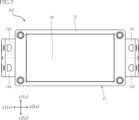
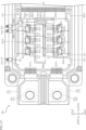
- FIG. 1 is a perspective view showing a semiconductor device according to a first embodiment.
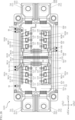
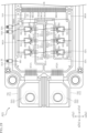
- FIG. 2 is a plan view showing the semiconductor device according to the first embodiment.
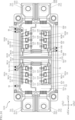
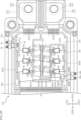
- FIG. 3 is a plan view of FIG. 2 with a part of the case (top plate) omitted.
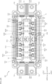
- FIG. 4 is a partially enlarged view of FIG. 3.
- FIG. 5 is a partially enlarged view of FIG. 3.
- FIG. 6 is a front view showing the semiconductor device according to the first embodiment.
- FIG. 7 is a bottom view showing the semiconductor device according to the first embodiment.
- FIG. 8 is a cross-sectional view taken along line VIII-VIII in FIG. 3.
- FIG. 9 is a cross-sectional view taken along line IX-IX in FIG. 3.
- FIG. 10 is a sectional view taken along line XX in FIG.
- FIG. 11 is a cross-sectional view taken along line XI-XI in FIG. 3.
- FIG. 12 is a sectional view taken along line XII-XII in FIG. 3.
- FIG. 13 is a cross-sectional view taken along line XIII-XIII in FIG.
- FIG. 14 is a plan view showing a semiconductor device according to a first modification of the first embodiment, with a part of the case (top plate) and a resin member omitted.
- FIG. 15 is a plan view showing a semiconductor device according to a second modification of the first embodiment, with a part of the case (top plate) and a resin member omitted.
- FIG. 16 is a plan view showing a semiconductor device according to a third modification of the first embodiment, with a part of the case (top plate) and a resin member omitted.
- FIG. 17 is an enlarged plan view of a main part of a semiconductor device according to a second embodiment.
- FIG. 18 is an enlarged plan view of a main part of a semiconductor device according to a second embodiment.
- FIG. 19 is an enlarged plan view of a main part of a semiconductor device according to a modification of the second embodiment.
- FIG. 20 is an enlarged plan view of main parts showing a semiconductor device according to a modification of the second embodiment.
- FIG. 21 is an enlarged plan view of main parts showing a semiconductor device according to a third embodiment.
- FIG. 22 is an enlarged plan view of a main part of a semiconductor device according to a third embodiment.
- FIG. 23 is an enlarged plan view of a main part of a semiconductor device according to a modification of the third embodiment.
- FIG. 24 is an enlarged plan view of a main part of a semiconductor device according to a modification of the third embodiment.
- FIG. 25 is a plan view showing the semiconductor device according to the fourth embodiment, with a part of the case (top plate) and a resin member omitted.
- a thing A is formed on a thing B" and "a thing A is formed on a thing B” mean “a thing A is formed on a thing B" unless otherwise specified.
- A is formed directly on something B
- a thing A is formed on something B, with another thing interposed between them.” including.
- "a certain thing A is placed on a certain thing B” and "a certain thing A is placed on a certain thing B” are used as "a certain thing A is placed on a certain thing B” unless otherwise specified.
- ⁇ It is placed directly on something B,'' and ⁇ A thing A is placed on something B, with another thing interposed between them.'' include.
- an object A is located on an object B
- an object A is in contact with an object B, and an object A is located on an object B.
- an object A overlaps an object B when viewed in a certain direction means, unless otherwise specified, “an object A overlaps all of an object B" and "a certain object A overlaps an object B".
- a certain thing A (the material of the thing) includes a certain material C” means "a case where the thing A (the material of the thing A) consists of a certain material C" and "the main component of the thing A (the material of the thing)”. "is a certain material C”.
- a certain object A is arranged (extends) along a certain direction B” means that a certain object A is arranged (extends) strictly in a certain direction B. It includes, but is not limited to, the range of error caused by, for example, manufacturing variations.
- a certain surface A faces (one side or the other side of) a certain direction B is not limited to the case where the angle of the surface A with respect to the direction B is 90 degrees; This includes the case where A is tilted with respect to direction B.
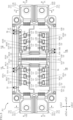
- the semiconductor device A1 includes a plurality of semiconductor elements 1, an insulating substrate 2, a plurality of wiring sections 3, a plurality of terminals, a plurality of connection members, a heat sink 70, and a case 71.
- the plurality of terminals include a first power terminal 51, a second power terminal 52, a pair of first signal terminals 53A, 53B, a pair of second signal terminals 54A, 54B, a signal terminal 55, and a pair of signal terminals 56.
- the plurality of connection members include a plurality of connection members 61A, 61B, a plurality of connection members 62A, 62B, a plurality of connection members 631A, 631B, 632A, 632B, a plurality of connection members 641A, 641B, 642A, 642B, and a plurality of connection members.
- the thickness direction z corresponds to the thickness direction of the semiconductor device A1.
- plane view refers to when viewed in the thickness direction z. Note that descriptions such as “upper”, “lower”, “upper”, “lower”, “upper surface”, and “lower surface” indicate the relative positional relationship of each component etc. in the thickness direction z, and do not necessarily mean It is not a term that defines the relationship with the direction of gravity.
- Each of the plurality of semiconductor elements 1 is, for example, a MOSFET.
- Each of the plurality of semiconductor elements 1 may be other switching elements such as a field effect transistor including a MISFET (Metal-Insulator-Semiconductor FET) or a bipolar transistor including an IGBT instead of a MOSFET.
- Each of the plurality of semiconductor elements 1 is, for example, an N-channel type and has a vertical structure.
- Each of the plurality of semiconductor elements 1 includes a compound semiconductor substrate.
- the composition of the compound semiconductor includes silicon carbide (SiC).
- the composition may include silicon (Si), gallium arsenide (GaAs), gallium nitride (GaN), or gallium oxide (Ga 2 O 3 ) instead of SiC.
- each of the plurality of semiconductor elements 1 has an element main surface 10a and an element back surface 10b.
- the element main surface 10a and the element back surface 10b are spaced apart from each other in the thickness direction z.
- the element main surface 10a faces upward in the thickness direction z (z1 side in the thickness direction z), and the element back surface 10b faces downward in the thickness direction z (z2 side in the thickness direction z).
- Each of the plurality of semiconductor elements 1 has a first electrode 101, a second electrode 102, and a third electrode 103, as shown in FIGS. 4, 5, 8, 9, 12, and 13.
- the first electrode 101 is arranged on the back surface 10b of the element.
- the second electrode 102 and the third electrode 103 are arranged on the element main surface 10a.
- a current corresponding to the power before being converted by the semiconductor element 1 flows through the first electrode 101 .
- a current corresponding to the power converted by the semiconductor element 1 flows through the second electrode 102 .
- a drive signal for driving the semiconductor element 1 is input to the third electrode 103 .
- Each semiconductor element 1 switches between a conductive state and a cut-off state according to a drive signal input to the third electrode 103.
- each semiconductor element 1 In a conductive state, a current flows from the first electrode 101 to the second electrode 102, and in a cutoff state, this current does not flow. That is, in each semiconductor element 1, the on/off control between the first electrode 101 and the second electrode 102 is controlled by the drive signal input to the third electrode 103.
- the first electrode 101 is a drain
- the second electrode 102 is a source
- the third electrode 103 is a gate.
- the aforementioned drive signal is a gate voltage.
- each semiconductor element 1 may have a fourth electrode having the same potential as the second electrode 102.
- the fourth electrode is arranged, for example, on one side or both sides of the third electrode 103 in the second direction y. In an example where each semiconductor element 1 is a MOSFET, the fourth electrode is source sense.
- Each of the plurality of semiconductor elements 1 is bonded to one of the plurality of wiring portions 3 using a conductive bonding material.
- the conductive bonding material is, for example, solder, sintered metal, or metal paste.
- the multiple semiconductor elements 1 include multiple first elements 11A, 11B and multiple second elements 12A, 12B.
- the plurality of semiconductor elements 1 include three first elements 11A, three first elements 11B, three second elements 12A, and three second elements 12B, but at least one The first element 11A, at least one first element 11B, at least one second element 12A, and at least one second element 12B may be included.
- each of the plurality of first elements 11A is mounted on one of the plurality of wiring sections 3 (first wiring section 31A to be described later).
- the plurality of first elements 11A are arranged along the first direction x.
- each of the plurality of first elements 11B is mounted on one of the plurality of wiring sections 3 (first wiring section 31B to be described later).
- the plurality of first elements 11B are arranged along the first direction x.
- the plurality of first elements 11B are arranged on the x1 side in the first direction x with respect to the plurality of first elements 11A.
- each of the plurality of second elements 12A is mounted on one of the plurality of wiring sections 3 (second wiring section 32A to be described later).
- the plurality of second elements 12A are arranged along the first direction x.
- the plurality of second elements 12A are located on the y2 side in the second direction y with respect to the plurality of first elements 11A.
- each of the plurality of second elements 12B is mounted on one of the plurality of wiring sections 3 (second wiring section 32B to be described later).
- the plurality of second elements 12B are arranged along the first direction x.
- the plurality of second elements 12B are located on the y2 side in the second direction y with respect to the plurality of first elements 11B.
- the plurality of second elements 12B are arranged on the x1 side in the first direction x with respect to the plurality of second elements 12A.
- each first electrode 101 (drain) of the plurality of first elements 11A and each first electrode 101 (drain) of the plurality of second elements 12A are electrically connected to each other, and
- Each second electrode 102 (source) of one element 11A and each second electrode 102 (source) of the plurality of second elements 12A are electrically connected to each other. That is, the plurality of first elements 11A and the plurality of second elements 12A are electrically connected in parallel.
- each first electrode 101 (drain) of the plurality of first elements 11B and each first electrode 101 (drain) of the plurality of second elements 12B are electrically connected to each other, and
- Each second electrode 102 (source) of one element 11B and each second electrode 102 (source) of the plurality of second elements 12B are electrically connected to each other. That is, the plurality of first elements 11B and the plurality of second elements 12B are electrically connected in parallel.
- each first electrode 101 (drain) of the plurality of first elements 11A and each first electrode 101 (drain) of the plurality of first elements 11B are electrically connected to each other, and Each first electrode 101 (drain) of the two elements 12A and each first electrode 101 (drain) of the plurality of second elements 12B are electrically connected to each other. In other words, the first electrodes 101 of the plurality of semiconductor elements 1 are electrically connected to each other.
- the heat sink 70 is, for example, a flat plate that is rectangular in plan view.
- the heat sink 70 is made of a material with high thermal conductivity, and includes, for example, copper or a copper alloy.
- the surface of the heat sink 70 may be plated with Ni.
- a cooling member for example, a heat sink
- the insulating substrate 2 is placed on the heat sink 70.
- FIGS. 8, 9, 12, and 13 the insulating substrate 2 is placed on the heat sink 70.
- the case 71 is, for example, a rectangular parallelepiped.
- the case 71 is made of synthetic resin that is electrically insulating and has excellent heat resistance.
- the synthetic resin includes, for example, PPS (polyphenylene sulfide).
- Case 71 has a rectangular shape with the same (or substantially the same) size as heat sink 70 in plan view.
- Case 71 includes a frame 72, a top plate 73, and a plurality of terminal blocks 741-744.
- the frame portion 72 is fixed to the surface of the heat sink 70 on the z1 side in the thickness direction z.
- the top plate 73 is fixed to the frame portion 72.
- the top plate 73 closes the opening on the z1 side in the thickness direction z of the frame portion 72, as shown in FIGS. 1, 2, 8, 9, 12, and 13.
- the top plate 73 faces a heat sink 70 that closes the z2 side of the frame 72 in the thickness direction z.
- a circuit accommodation space (a space for accommodating a plurality of semiconductor elements 1 and the like) is defined inside the case 71 by the top plate 73, the heat sink 70, and the frame 72.
- this circuit housing space may be referred to as the inside of the case 71.
- the two terminal blocks 741 and 742 are arranged on the x2 side in the first direction x than the frame portion 72 and are integrally formed with the frame portion 72.
- the two terminal blocks 743 and 744 are arranged on the x1 side in the first direction x than the frame portion 72 and are integrally formed with the frame portion 72.
- the two terminal blocks 741 and 742 are arranged along the second direction y with respect to the side wall of the frame portion 72 on the x2 side in the first direction x.
- the terminal block 741 covers a part of the first power terminal 51 (first terminal section 51A, which will be described later).
- a part of the first terminal portion 51A is arranged on the surface of the terminal block 741 on the z1 side in the thickness direction z.
- the terminal block 742 covers a part of the second power terminal 52 (a third terminal portion 52A to be described later). A part of the third terminal portion 52A is arranged on the surface of the terminal block 742 on the z1 side in the thickness direction z.
- the two terminal blocks 743 and 744 are arranged along the second direction y with respect to the side wall of the frame portion 72 on the x1 side in the first direction x.
- the terminal block 743 covers a part of the first power terminal 51 (second terminal section 51B, which will be described later).
- a part of the second terminal portion 51B is arranged on the surface of the terminal block 743 on the z1 side in the thickness direction z.
- the terminal block 744 covers a part of the second power terminal 52 (fourth terminal section 52B, which will be described later).
- a part of the fourth terminal portion 52B is arranged on the surface of the terminal block 744 on the z1 side in the thickness direction z.
- the semiconductor device A1 further includes a resin member 75. As shown in FIGS. 8, 9, 12, and 13, the resin member 75 is filled in the area surrounded by the top plate 73, the heat sink 70, and the frame 72 (the circuit housing space).
- the resin member 75 covers the plurality of semiconductor elements 1 and the like.
- the resin member 75 is made of, for example, black epoxy resin.
- the constituent material of the resin member 75 may be other insulating materials such as silicone gel instead of epoxy resin.
- the semiconductor device A1 is not limited to the configuration including the resin member 75, and may not include the resin member 75.
- the insulating substrate 2 is electrically insulating.
- the composition of the insulating substrate 2 includes, for example, ceramics having excellent thermal conductivity. Examples of such ceramics include AlN (aluminum nitride), SiN (silicon nitride), and Al 2 O 3 (aluminum oxide).
- the insulating substrate 2 is, for example, a flat plate.
- the insulating substrate 2 has a substrate main surface 21 and a substrate back surface 22, as shown in FIGS. 8, 9, 12, and 13.
- the substrate main surface 21 and the substrate back surface 22 are spaced apart from each other in the thickness direction z.
- the main surface 21 of the substrate faces upward in the thickness direction z (the z1 side in the thickness direction z), and the back surface 22 of the substrate faces downward in the thickness direction z (the z2 side in the thickness direction z).
- the plurality of semiconductor elements 1 are arranged on the main surface 21 of the substrate.
- the back surface 22 of the substrate faces the heat sink 70 .
- a metal layer may be formed on the back surface 22 of the substrate. Therefore, a metal layer may be formed between the insulating substrate 2 and the heat sink 70.
- the metal layer may be made of the same material as the plurality of wiring parts 3.
- the plurality of wiring portions 3 are formed on the substrate main surface 21 of the insulating substrate 2.
- the plurality of wiring parts 3 are, for example, metal layers.
- the composition of this metal layer includes, but is not limited to, copper.
- the plurality of wiring parts 3 include a pair of first wiring parts 31A, 31B, a pair of second wiring parts 32A, 32B, a pair of third wiring parts 33A, 33B, and a pair of connection wiring parts 34A, 34B.
- the plurality of wiring parts 3 include a pair of first signal wiring parts 351A, 351B, a pair of signal wiring parts 352A, 352B, a pair of signal wiring parts 353A, 353B, a pair of second signal wiring parts 362A, 362B, a pair of signal wiring parts 352A, 352B, a pair of signal wiring parts 353A, 353B, , a pair of fourth signal wiring sections 361A, 361B, and a pair of signal wiring sections 37.
- a pair of first wiring portions 31A, 31B, a pair of second wiring portions 32A, 32B, a pair of third wiring portions 33A, 33B, and a pair of connection wiring portions 34A, 34B provide a main current conduction path in semiconductor device A1. Eggplant. The main current is generated by the switching operation of the plurality of semiconductor elements 1.
- a plurality of first elements 11A are mounted on the first wiring section 31A.
- Each first electrode 101 (drain) of the plurality of first elements 11A is bonded to the first wiring portion 31A via the above-mentioned conductive bonding material. Therefore, the first wiring portion 31A is electrically connected to each first electrode 101 of the plurality of first elements 11A.
- a plurality of connection members 671A are joined to the first wiring portion 31A.
- the first wiring section 31A is electrically connected to the first power terminal 51 (first terminal section 51A, which will be described later) via a plurality of connection members 671A.
- a plurality of first elements 11B are mounted on the first wiring section 31B.
- Each first electrode 101 (drain) of the plurality of first elements 11B is bonded to the first wiring portion 31B via the aforementioned conductive bonding material. Therefore, the first wiring portion 31B is electrically connected to each first electrode 101 of the plurality of first elements 11B.
- a plurality of connection members 671B are joined to the first wiring portion 31B.
- the first wiring section 31B is electrically connected to the first power terminal 51 (second terminal section 51B described later) via a plurality of connection members 671B.
- the first wiring section 31B is spaced apart from the first wiring section 31A in the first direction x.
- the first wiring section 31B is located on the x1 side in the first direction x with respect to the first wiring section 31A.
- a plurality of second elements 12A are mounted on the second wiring section 32A.
- Each first electrode 101 (drain) of the plurality of second elements 12A is bonded to the second wiring portion 32A via the above-mentioned conductive bonding material. Therefore, the second wiring portion 32A is electrically connected to each first electrode 101 of the plurality of second elements 12A.
- the second wiring section 32A is located on the y2 side in the second direction y with respect to the first wiring section 31A.
- a plurality of second elements 12B are mounted on the second wiring section 32B.
- Each first electrode 101 (drain) of the plurality of second elements 12B is bonded to the second wiring portion 32B via the aforementioned conductive bonding material. Therefore, the second wiring portion 32B is electrically connected to each first electrode 101 of the plurality of second elements 12B.
- the second wiring section 32B is spaced apart from the second wiring section 32A in the first direction x.
- the second wiring section 32B is located on the x1 side in the first direction x with respect to the second wiring section 32A.
- the second wiring section 32B is located on the y2 side in the second direction y with respect to the first wiring section 31B.
- the third wiring section 33A is located between the first wiring section 31A and the second wiring section 32A in the second direction y.
- a plurality of connection members 61A are joined to the third wiring portion 33A.
- the third wiring portion 33A is electrically connected to the second electrodes 102 (sources) of the plurality of first elements 11A via the plurality of connection members 61A.
- a plurality of connection members 62A are joined to the third wiring portion 33A.
- the third wiring portion 33A is electrically connected to the second electrodes 102 (sources) of the plurality of second elements 12A via the plurality of connection members 62A.
- the second electrodes 102 of the plurality of first elements 11A and the second electrodes 102 of the plurality of second elements 12A are electrically connected to each other. Furthermore, a plurality of connection members 672A are joined to the third wiring portion 33A.
- the third wiring section 33A is electrically connected to the second power terminal 52 (a third terminal section 52A to be described later) via a plurality of connection members 672A.
- the third wiring section 33B is located between the first wiring section 31B and the second wiring section 32B in the second direction y.
- a plurality of connection members 61B are joined to the third wiring portion 33B.
- the third wiring section 33B is electrically connected to the second electrodes 102 (sources) of the plurality of first elements 11B via the plurality of connection members 61B.
- a plurality of connection members 62B are joined to the third wiring portion 33B.
- the third wiring portion 33B is electrically connected to the second electrodes 102 (sources) of the plurality of second elements 12B via the plurality of connection members 62B.
- the second electrodes 102 of the plurality of first elements 11B and the second electrodes 102 of the plurality of second elements 12B are electrically connected to each other. Furthermore, a plurality of connection members 672B are joined to the third wiring portion 33B.
- the third wiring section 33B is electrically connected to the second power terminal 52 (fourth terminal section 52B, which will be described later) via a plurality of connection members 672B.
- the third wiring section 33B is spaced apart from the third wiring section 33A in the first direction x.
- the third wiring section 33B is located on the x1 side in the first direction x with respect to the third wiring section 33A.
- the connecting wiring section 34A is connected to the first wiring section 31A and the second wiring section 32A.
- the first wiring section 31A, the second wiring section 32A, and the connection wiring section 34A are integrally formed.
- the connecting wiring section 34A is located on the x1 side in the first direction x with respect to the third wiring section 33A.
- the connecting wiring portion 34A is connected to an edge of the first wiring portion 31A on the x1 side in the first direction x and an edge of the second wiring portion 32A on the x1 side in the first direction x.
- the connecting wiring section 34B is connected to the first wiring section 31B and the second wiring section 32B.
- the first wiring section 31B, the second wiring section 32B, and the connection wiring section 34B are integrally formed.
- the connecting wiring section 34B is located on the x2 side in the first direction x with respect to the third wiring section 33B.
- the connecting wiring portion 34B is connected to an edge of the first wiring portion 31B on the x2 side in the first direction x and an edge of the second wiring portion 32B on the x2 side in the first direction x. With this configuration, the first wiring section 31B and the second wiring section 32B are electrically connected to each other via the connection wiring section 34B.
- the connecting wiring section 34B is spaced apart from the connecting wiring section 34A in the first direction x.
- the connecting wiring section 34B is located on the x1 side in the first direction x with respect to the connecting wiring section 34A.
- the pair of connection wiring parts 34A, 34B are electrically connected to each other via the plurality of connection members 670.
- the first electrodes 101 (drains) of the plurality of semiconductor elements 1 are electrically connected to each other.
- a pair of first signal wiring parts 351A, 351B, a pair of signal wiring parts 352A, 352B, and a pair of signal wiring parts 353A, 353B are each a drive for controlling the driving (switching operation) of a plurality of semiconductor elements 1. transmit signals.
- the first signal wiring section 351A, the signal wiring section 352A, and the signal wiring section 353A transmit a first drive signal for controlling the driving of the plurality of first elements 11A and the plurality of second elements 12A.
- the first signal wiring section 351B, the signal wiring section 352B, and the signal wiring section 353B transmit a second drive signal for controlling the driving of the plurality of first elements 11B and the plurality of second elements 12B.
- the frequency, phase, amplitude, etc. of the first drive signal and the second drive signal may be the same or different.
- the first signal wiring section 351A is located between the first wiring section 31A and the second wiring section 32A in the second direction y.
- the first signal wiring section 351A has a band shape whose longitudinal direction is the second direction y when viewed from above.
- the first signal wiring section 351A is located between the third wiring section 33A and the connection wiring section 34A in the first direction x.
- the first signal wiring section 351B is located between the first wiring section 31B and the second wiring section 32B in the second direction y.
- the first signal wiring section 351B has a band shape whose longitudinal direction is the second direction y when viewed from above.
- the first signal wiring section 351B is located between the third wiring section 33B and the connection wiring section 34B in the first direction x.
- the signal wiring section 352A is located on the opposite side of the first signal wiring section 351A and the plurality of second elements 12A with respect to the plurality of first elements 11A in the second direction y.
- the signal wiring section 352A is located on the y1 side in the second direction y with respect to the plurality of first elements 11A.
- the signal wiring section 352A is located closer to the y1 side in the second direction y than the first wiring section 31A.
- the signal wiring section 352A has a band shape whose longitudinal direction is the first direction x when viewed from above.
- the signal wiring section 352B is located on the opposite side of the first signal wiring section 351B and the plurality of second elements 12B with respect to the plurality of first elements 11B in the second direction y.
- the signal wiring section 352B is located on the y1 side in the second direction y with respect to the plurality of first elements 11B.
- the signal wiring section 352B is located closer to the y1 side in the second direction y than the first wiring section 31B.
- the signal wiring portion 352B has a band shape whose longitudinal direction is the first direction x when viewed from above.
- the signal wiring section 353A is located on the opposite side of the first signal wiring section 351A and the plurality of first elements 11A with respect to the plurality of second elements 12A in the second direction y.
- the signal wiring section 353A is located on the y2 side in the second direction y with respect to the plurality of second elements 12A.
- the signal wiring section 353A is located closer to the y2 side in the second direction y than the second wiring section 32A.
- the signal wiring section 353A has a band shape whose longitudinal direction is the first direction x when viewed from above.
- the signal wiring section 353B is located on the opposite side of the first signal wiring section 351B and the plurality of first elements 11B with respect to the plurality of second elements 12B in the second direction y.
- the signal wiring section 353B is located on the y2 side in the second direction y with respect to the plurality of second elements 12B.
- the signal wiring section 353B is located closer to the y2 side in the second direction y than the second wiring section 32B.
- the signal wiring section 353B has a band shape whose longitudinal direction is the first direction x in plan view.
- a pair of second signal wiring sections 362A, 362B, a pair of third signal wiring sections 363A, 363B, and a pair of fourth signal wiring sections 361A, 361B are respectively configured to detect the driving states of the plurality of semiconductor elements 1. Transmit the detection signal.
- the second signal wiring section 362A, the third signal wiring section 363A, and the fourth signal wiring section 361A are the first signal wiring section 362A, the third signal wiring section 363A, and the fourth signal wiring section 361A.
- the second signal wiring section 362B, the third signal wiring section 363B, and the fourth signal wiring section 361B transmit the detection signal
- the second signal wiring section 362B, the third signal wiring section 363B, and the fourth signal wiring section 361B are configured to transmit a detection signal.
- 2 detection signal is transmitted.
- the detection signals (first detection signal and second detection signal) are, for example, voltage signals corresponding to the current (source current) flowing through the second electrode 102 of each semiconductor element 1.
- the second signal wiring section 362A is located on the opposite side (signal wiring 352A).
- the second signal wiring section 362A is located on the y1 side in the second direction y with respect to the plurality of first elements 11A.
- the second signal wiring section 362A is located closer to the y1 side in the second direction y than the first wiring section 31A.
- the second signal wiring section 362A has a band shape whose longitudinal direction is the first direction x in plan view. In plan view, a part of the second signal wiring part 362A is arranged parallel to a part of the signal wiring part 352A.
- the second signal wiring section 362A is arranged on the y2 side in the second direction y than the signal wiring section 352A, but on the contrary, it may be arranged on the y1 side in the second direction y. good.
- the second signal wiring section 362B is located on the opposite side (signal wiring 352B).
- the second signal wiring section 362B is located on the y1 side in the second direction y with respect to the plurality of first elements 11B.
- the second signal wiring section 362B is located closer to the y1 side in the second direction y than the first wiring section 31B.
- the second signal wiring section 362B has a band shape whose longitudinal direction is the first direction x in plan view. In plan view, a part of the second signal wiring part 362B is arranged parallel to a part of the signal wiring part 352B.
- the second signal wiring section 362B is arranged on the y2 side in the second direction y than the signal wiring section 352B, but on the contrary, it may be arranged on the y1 side in the second direction y. good.
- the third signal wiring section 363A is located on the opposite side of the first signal wiring section 351A and the plurality of first elements 11A (signal wiring 353A).
- the third signal wiring section 363A is located on the y2 side in the second direction y with respect to the plurality of second elements 12A.
- the third signal wiring section 363A is located closer to the y2 side in the second direction y than the second wiring section 32A.
- the third signal wiring section 363A has a band shape whose longitudinal direction is the first direction x in plan view. In plan view, a portion of the third signal wiring section 363A is arranged parallel to a portion of the signal wiring section 353A.
- the third signal wiring section 363A is arranged on the y1 side in the second direction y relative to the signal wiring section 353A, but on the contrary, it may be arranged on the y2 side in the second direction y. good.
- the third signal wiring section 363B is located on the opposite side (signal wiring 353B).
- the third signal wiring section 363B is located on the y2 side in the second direction y with respect to the plurality of second elements 12B.
- the third signal wiring section 363B is located closer to the y2 side in the second direction y than the second wiring section 32B.
- the third signal wiring section 363B has a band shape whose longitudinal direction is the first direction x in plan view. In plan view, a portion of the third signal wiring section 363B is arranged parallel to a portion of the signal wiring section 353B.
- the third signal wiring section 363B is arranged on the y1 side in the second direction y relative to the signal wiring section 353B, but on the contrary, it may be arranged on the y2 side in the second direction y. good.
- the fourth signal wiring section 361A is located between the first wiring section 31A and the second wiring section 32A in the second direction y.
- the fourth signal wiring section 361A has a band shape whose longitudinal direction is the second direction y when viewed from above.
- the fourth signal wiring section 361A is located between the third wiring section 33A and the connection wiring section 34A in the first direction x.
- the fourth signal wiring section 361A is arranged parallel to the first signal wiring section 351A in plan view. In the illustrated example, the fourth signal wiring section 361A is arranged on the x2 side in the first direction x with respect to the first signal wiring section 351A, but on the contrary, it is arranged on the x1 side in the first direction x. may have been done.
- the fourth signal wiring section 361B is located between the first wiring section 31B and the second wiring section 32B in the second direction y.
- the fourth signal wiring section 361B has a band shape whose longitudinal direction is the second direction y when viewed from above.
- the fourth signal wiring section 361B is located between the third wiring section 33B and the connection wiring section 34B in the first direction x.
- the fourth signal wiring section 361B is arranged parallel to the first signal wiring section 351B in plan view. In the illustrated example, the fourth signal wiring section 361B is arranged on the x1 side in the first direction x with respect to the first signal wiring section 351B, but on the contrary, it is arranged on the x2 side in the first direction x. may have been done.
- the pair of signal wiring sections 37 are spaced apart from each other in the first direction x.
- a thermistor 91 is connected to each of the pair of signal wiring sections 37 .
- the thermistor 91 is placed across the pair of signal wiring sections 37 .
- the thermistor 91 may not be bonded to the pair of signal wiring sections 37.
- the pair of signal wiring sections 37 are located near the corners of the insulating substrate 2.
- the pair of signal wiring sections 37 are located between the first wiring section 31B, the signal wiring section 352B, and the second signal wiring section 362B in the first direction x. Further, the pair of signal wiring sections 37 are located on the y1 side in the second direction y with respect to a part of the first wiring section 31B.
- the plurality of connection members connects two parts that are spaced apart from each other with each other.
- the plurality of connection members include a plurality of connection members 61A, 61B, a plurality of connection members 62A, 62B, a plurality of connection members 631A, 631B, 632A, 632B, a plurality of connection members 641A, 641B, 642A, 642B, and a plurality of connection members.
- Each of these connecting members is a bonding wire.
- the composition of the bonding wire includes either gold, silver, copper or aluminum. Note that each of the plurality of connection members may be a metal plate instead of a bonding wire.
- the plurality of connection members 61A are joined to the second electrodes 102 of the plurality of first elements 11A and the third wiring portion 33A to electrically connect them.
- three connecting members 61A are connected to each first element 11A, but the number of connecting members 61A connected to each first element 11A is not limited to this.
- the number of connection members 61A can be changed as appropriate depending on the magnitude of the current flowing through the second electrode 102 of each first element 11A.
- the plurality of connection members 62A are joined to the second electrodes 102 of the plurality of second elements 12A and the third wiring part 33A, and electrically connect them.
- three connecting members 62A are connected to each second element 12A, but the number of connecting members 62A connected to each second element 12A is not limited to this.
- the number of connection members 62A can be changed as appropriate depending on the magnitude of the current flowing through the second electrode 102 of each second element 12A.
- the second electrodes 102 of the plurality of first elements 11A and the second electrodes 102 of the plurality of second elements 12A are electrically connected to each other.
- the plurality of connection members 61B are joined to the second electrodes 102 and third wiring portions 33B of the plurality of first elements 11B to electrically connect them.
- three connecting members 61B are connected to each first element 11B, but the number of connecting members 61B connected to each first element 11B is not limited to this.
- the number of connection members 61B can be changed as appropriate depending on the magnitude of the current flowing through the second electrode 102 of each first element 11B.
- connection members 62B are joined to the second electrodes 102 of the plurality of second elements 12B and the third wiring portions 33B to electrically connect them.
- three connection members 62B are connected to each second element 12B, but the number of connection members 62B connected to each second element 12B is not limited to this. The number of connection members 62B can be changed as appropriate depending on the magnitude of the current flowing through the second electrode 102 of each second element 12B.
- the second electrodes 102 of the plurality of first elements 11B and the second electrodes 102 of the plurality of second elements 12B are electrically connected to each other.
- the plurality of connection members 631A are individually joined to the third electrode 103 of each first element 11A and the signal wiring section 352A, and electrically connect them.
- the plurality of connection members 632A are individually joined to the third electrode 103 of each second element 12A and the signal wiring section 353A to electrically connect them.
- the plurality of connection members 631B are individually joined to the third electrode 103 of each first element 11B and the signal wiring section 352B, and electrically connect them.
- the plurality of connection members 632B are individually joined to the third electrode 103 of each second element 12B and the signal wiring section 353B to electrically connect them.
- the plurality of connection members 641A are individually joined to the second electrode 102 of each first element 11A and the second signal wiring section 362A to electrically connect them.
- the plurality of connection members 642A are individually joined to the second electrode 102 of each second element 12A and the third signal wiring section 363A to electrically connect them.
- the plurality of connection members 641B are individually joined to the second electrode 102 of each first element 11B and the second signal wiring section 362B to electrically connect them.
- the plurality of connection members 642B are individually joined to the second electrode 102 of each second element 12B and the third signal wiring section 363B to electrically connect them.
- the connecting member 650A is joined to the first signal terminal 53A and the signal wiring section 352A to electrically connect them.
- the connecting member 651A is joined to the first signal wiring section 351A and the signal wiring section 352A to electrically connect them.
- the connecting member 652A is joined to the first signal wiring section 351A and the signal wiring section 353A to electrically connect them.
- the third electrode 103 of each first element 11A is electrically connected to the signal wiring section 352A via the connecting member 631A
- the third electrode 103 of each second element 12A is electrically connected to the connecting member 632A. Since the first signal terminal 53A is electrically connected to the signal wiring section 353A through the signal wiring section 353A, the first signal terminal 53A is electrically electrically connected to each third electrode 103 of the plurality of first elements 11A and to each third electrode 103 of the plurality of second elements 12A.
- the connecting member 660A is joined to the second signal terminal 54A and the second signal wiring section 362A to electrically connect them.
- the connecting member 661A is joined to the fourth signal wiring section 361A and the second signal wiring section 362A to electrically connect them.
- the connecting member 662A is joined to the fourth signal wiring section 361A and the third signal wiring section 363A to electrically connect them. With such a configuration, the fourth signal wiring section 361A, the second signal wiring section 362A, and the third signal wiring section 363A are electrically connected to each other and to the second signal terminal 54A.
- the second electrode 102 of each first element 11A is electrically connected to the second signal wiring section 362A via the connecting member 641A, and the second electrode 102 of each second element 12A is electrically connected to the connecting member 642A. Since the second signal terminal 54A is electrically connected to the third signal wiring section 363A through the third signal wiring section 363A, the second signal terminal 54A is electrically connected to each second electrode 102 of the plurality of first elements 11A and to each second electrode 102 of the plurality of second elements 12A.
- the connecting member 650B is joined to the first signal terminal 53B and the signal wiring section 353B to electrically connect them.
- the connecting member 651B is joined to the first signal wiring section 351B and the signal wiring section 352B to electrically connect them.
- the connecting member 652B is joined to the first signal wiring section 351B and the signal wiring section 353B to electrically connect them.
- the third electrode 103 of each first element 11B is electrically connected to the signal wiring section 352B via the connecting member 631B
- the third electrode 103 of each second element 12B is electrically connected to the connecting member 632B. Since the first signal terminal 53B is electrically connected to the signal wiring section 353B through the signal wiring section 353B, the first signal terminal 53B is electrically connected to each third electrode 103 of the plurality of first elements 11B and each third electrode 103 of the plurality of second elements 12B.
- the connecting member 660B is joined to the second signal terminal 54B and the third signal wiring section 363B to electrically connect them.
- the connecting member 661B is joined to the fourth signal wiring section 361B and the second signal wiring section 362B to electrically connect them.
- the connecting member 662B is joined to the fourth signal wiring section 361B and the third signal wiring section 363B to electrically connect them.
- the second electrode 102 of each first element 11B is electrically connected to the second signal wiring section 362B via the connecting member 641B, and the second electrode 102 of each second element 12B is connected to the connecting member 642B.
- the second signal terminal 54B is electrically connected to each second electrode 102 of the plurality of first elements 11B and to each second electrode 102 of the plurality of second elements 12B. .
- connection members 670 are joined to each of the pair of connection wiring parts 34A, 34B to electrically connect them. With such a configuration, the connecting wiring portion 34A and the connecting wiring portion 34B are electrically connected to each other.
- the plurality of connection members 671A are respectively joined to the first terminal portion 51A and the first wiring portion 31A to electrically connect them.
- the first wiring portion 31A is electrically connected to each first electrode 101 of the plurality of first elements 11A and each first electrode 101 of the plurality of second elements 12A, so that the first terminal portion 51A is Conductivity is established between each first electrode 101 of the plurality of first elements 11A and each first electrode 101 of the plurality of second elements 12A.
- the plurality of connection members 671B are respectively joined to the second terminal portion 51B and the first wiring portion 31B to electrically connect them.
- the semiconductor device A1 since the first wiring section 31B is electrically connected to each first electrode 101 of the plurality of first elements 11B and each first electrode 101 of the plurality of second elements 12B, the second terminal section 51B is The first electrodes 101 of the plurality of first elements 11B and the first electrodes 101 of the plurality of second elements 12B are electrically connected.
- the plurality of connection members 672A are respectively joined to the third terminal portion 52A and the third wiring portion 33A to electrically connect them.
- the third wiring section 33A is electrically connected to each second electrode 102 of the plurality of first elements 11A and each second electrode 102 of the plurality of second elements 12A
- the third terminal section 52A is It is electrically connected to each second electrode 102 of the plurality of first elements 11A and to each second electrode 102 of the plurality of second elements 12A.
- the plurality of connection members 672B are respectively joined to the fourth terminal portion 52B and the third wiring portion 33B to electrically connect them.
- the fourth terminal section 52B is It is electrically connected to each second electrode 102 of the plurality of first elements 11B and to each second electrode 102 of the plurality of second elements 12B.
- connection member 681 is joined to the signal terminal 55 and the first wiring portion 31A to electrically connect them.
- the pair of connecting members 682 are individually joined to the pair of signal terminals 56 and the pair of signal wiring portions 37 to electrically connect them.
- a portion of each of the pair of signal terminals 56 is exposed from the case 71, as shown in FIGS. 1 and 2, respectively.
- the composition of each of the first power terminal 51, the second power terminal 52, the pair of first signal terminals 53A, 53B, the pair of second signal terminals 54A, 54B, the signal terminal 55, and the pair of signal terminals 56 includes, for example, copper. .
- Each of the compositions may contain metals other than copper.
- the first power terminal 51 is electrically connected to the pair of first wiring parts 31A and 31B.
- the first power terminal 51 is electrically connected to each first electrode 101 (drain) of the plurality of semiconductor elements 1 (the plurality of first elements 11A, 11B and the plurality of second elements 12A, 12B).
- the first power terminal 51 includes a first terminal portion 51A and a second terminal portion 51B, as shown in FIGS. 4 and 5.
- the first terminal portion 51A and the second terminal portion 51B are arranged on opposite sides of the insulating substrate 2 in the first direction. As shown in FIG. 4, FIG. 8, and FIG. z facing the z1 side).
- a plurality of connection members 671A are joined to a portion of the first terminal portion 51A that is disposed inside the case 71.
- the first terminal portion 51A is electrically connected to the first wiring portion 31A via the plurality of connection members 671A. As shown in FIG. 5, FIG. 8, and FIG. z facing the z1 side).
- connection members 671B are joined to a portion of the second terminal portion 51B that is disposed inside the case 71.
- the second terminal portion 51B is electrically connected to the first wiring portion 31B via a plurality of connection members 671B. Therefore, the first terminal portion 51A and the second terminal portion 51B are connected to each of the first electrodes 101 (drains) of the plurality of semiconductor elements 1 (the plurality of first elements 11A, 11B and the plurality of second elements 12A, 12B). Conduct.
- the second power terminal 52 is electrically connected to the pair of third wiring portions 33A and 33B.
- the second power terminal 52 is electrically connected to each second electrode 102 (source) of the plurality of semiconductor elements 1 (the plurality of first elements 11A, 11B and the plurality of second elements 12A, 12B).
- the second power terminal 52 includes a third terminal portion 52A and a fourth terminal portion 52B, as shown in FIGS. 4 and 5.
- the third terminal portion 52A and the fourth terminal portion 52B are arranged on opposite sides of the insulating substrate 2 in the first direction x. As shown in FIG. 5, FIG. 9, and FIG. z facing the z1 side).
- a plurality of connection members 672A are joined to a portion of the third terminal portion 52A that is disposed inside the case 71.
- the third terminal portion 52A is electrically connected to the third wiring portion 33A via a plurality of connection members 672A. Therefore, the third terminal portion 52A is electrically connected to each second electrode 102 (source) of the plurality of first elements 11A and the plurality of second elements 12A.
- the third terminal portion 52A is located on the y2 side in the second direction y with respect to the first terminal portion 51A.
- the fourth terminal portion 52B includes a portion disposed inside the case 71, a portion embedded in the terminal block 744, and a surface (thickness z facing the z1 side).
- a plurality of connection members 672B are joined to a portion of the fourth terminal portion 52B that is disposed inside the case 71.
- the fourth terminal portion 52B is electrically connected to the third wiring portion 33B via a plurality of connection members 672B. Therefore, the fourth terminal portion 52B is electrically connected to each second electrode 102 (source) of the plurality of first elements 11B and second elements 12B.
- the fourth terminal portion 52B is located on the y2 side in the second direction y with respect to the first terminal portion 51A.
- the first signal terminal 53A is electrically connected to the signal wiring section 352A via the connecting member 650A.
- the first signal terminal 53A is electrically connected to each third electrode 103 (gate) of the plurality of first elements 11A and the plurality of second elements 12A.
- the first signal terminal 53B is electrically connected to the signal wiring section 353B via the connecting member 650B.
- the first signal terminal 53B is electrically connected to each third electrode 103 (gate) of the plurality of first elements 11B and the plurality of second elements 12B.
- the pair of first signal terminals 53A and 53B are each input terminals for the aforementioned drive signal.
- the pair of first signal terminals 53A and 53B are each gate terminals.
- the pair of first signal terminals 53A and 53B each include a part disposed inside the case 71, a part embedded in the frame part 72, and a rod-shaped part protruding from the frame part 72 toward the z1 side in the thickness direction z. including.
- the aforementioned pair of connecting members 650A and 650B are individually joined to portions of the pair of first signal terminals 53A and 53B that are arranged inside the case 71.
- the second signal terminal 54A is electrically connected to the second signal wiring section 362A via the connecting member 660A.
- the second signal terminal 54A is electrically connected to each second electrode 102 (source) of the plurality of first elements 11A and the plurality of second elements 12A.
- the second signal terminal 54B is electrically connected to the third signal wiring section 363B via a connecting member 660B.
- the second signal terminal 54B is electrically connected to each second electrode 102 (source) of the plurality of first elements 11B and the plurality of second elements 12B.
- the pair of second signal terminals 54A and 54B are respectively output terminals for the aforementioned detection signal.
- the pair of second signal terminals 54A and 54B are each source sense terminals.
- the pair of second signal terminals 54A and 54B each include a part disposed inside the case 71, a part embedded in the frame part 72, and a rod-shaped part protruding from the frame part 72 toward the z1 side in the thickness direction z. including.
- the aforementioned pair of connecting members 660A and 660B are individually joined to portions of the pair of second signal terminals 54A and 54B that are arranged inside the case 71.
- the signal terminal 55 is electrically connected to the first wiring portion 31A via the connecting member 681.
- the signal terminal 55 is electrically connected to each first electrode 101 (drain) of the plurality of semiconductor elements 1 (particularly the plurality of first elements 11A).
- the signal terminal 55 is, for example, a drain sense terminal.
- the signal terminal 55 includes a portion disposed inside the case 71, a portion embedded in the frame portion 72, and a rod-shaped portion protruding from the frame portion 72 toward the z1 side in the thickness direction z.
- the aforementioned connecting member 681 is joined to a portion of the signal terminal 55 located inside the case 71.
- the pair of signal terminals 56 are individually electrically connected to the pair of signal wiring sections 37 via a pair of connecting members 682.
- the pair of signal terminals 56 are temperature detection terminals.
- Each of the pair of signal terminals 56 includes a portion disposed inside the case 71, a portion embedded in the frame portion 72, and a rod-shaped portion protruding from the frame portion 72 toward the z1 side in the thickness direction z.
- the aforementioned pair of connecting members 682 are individually joined to portions of the pair of signal terminals 56 that are arranged inside the case 71.
- the functions and effects of the semiconductor device A1 are as follows.
- the plurality of semiconductor elements 1 include at least one first element 11A (in the illustrated example, a plurality of first elements 11A) mounted on the first wiring part 31A, and at least one first element 11A mounted on the second wiring part 32A. at least one second element 12A (in the illustrated example, a plurality of second elements 12A).
- the first wiring part 31A is electrically connected to each first electrode 101 of at least one first element 11A
- the second wiring part 32A is electrically connected to each first electrode 101 of at least one second element 12B.
- the third wiring section 33A is electrically connected to each second electrode 102 of the plurality of semiconductor elements 1 (at least one first element 11A and at least one second element 12A), and is electrically connected to the first wiring in the second direction y.
- each second electrode 102 of at least one first element 11A and each second electrode 102 of at least one second element 12A are electrically connected to each other; It is possible to arrange one element 11A and at least one second element 12A in two rows.
- the plurality of first elements 11A are arranged along the first direction x
- the plurality of second elements 12A are arranged along the first direction x, so that these are arranged in two rows. are arranged.
- the semiconductor device A1 can suppress the plurality of semiconductor elements 1 from being arranged along one direction, the plurality of semiconductor elements 1 (at least one Even when arranging one element 11A and at least one second element 12A), it is possible to suppress deviation in the ratio of the long side to the short side in plan view.
- each second electrode 102 of at least one first element 11B and each second electrode 102 of at least one second element 12B are electrically connected to each other. It is possible to arrange the elements 11B and at least one second element 12B in two rows. Therefore, even if the semiconductor device A1 includes a plurality of semiconductor elements 1 (at least one first element 11B and at least one second element 12B) in which the second electrodes 102 are electrically connected to each other, , it becomes possible to suppress bias in the ratio of the long side to the short side in plan view.
- the plurality of wiring parts 3 include a connecting wiring part 34A that connects the first wiring part 31A and the second wiring part 32A.
- the first electrodes 101 of the plurality of semiconductor elements 1 are electrically connected to each other.
- the semiconductor device A1 even when at least one first element 11A and at least one second element 12A (a plurality of semiconductor elements 1) are electrically connected in parallel, the long side in plan view It becomes possible to suppress the bias in the ratio with respect to the short side.
- At least one first element 11B and at least one second element 12B This also applies to at least one first element 11B and at least one second element 12B. That is, in the semiconductor device A1, since the plurality of wiring parts 3 include the connecting wiring part 34B that connects the first wiring part 31B and the second wiring part 32B, at least one first element 11B and at least one second Even when the elements 12B (semiconductor elements 1) are electrically connected in parallel, it is possible to suppress deviation in the ratio of the long side to the short side in plan view.
- the semiconductor device A1 includes a connecting member 670 that connects the connecting wiring section 34A and the connecting wiring section 34B. According to such a configuration, the first electrodes 101 of at least one first element 11A, at least one first element 11B, at least one second element 12A, and at least one second element 12B are electrically connected to each other. connected. In other words, the semiconductor device A1 includes all of the plurality of semiconductor elements 1 (at least one first element 11A, at least one first element 11B, at least one second element 12A, and at least one second element 12B). Even when the first electrodes 101 are electrically connected to each other, it is possible to suppress deviation in the ratio of the long side to the short side in plan view.
- FIG. 14 shows a semiconductor device A11 according to a first modification of the first embodiment.
- the semiconductor device A11 differs from the semiconductor device A1 in that it does not include any of the plurality of connection members 670. Since the semiconductor device A11 does not include any of the plurality of connecting members 670, the connecting wiring section 34A and the connecting wiring section 34B are electrically insulated.
- FIG. 15 shows a semiconductor device A12 according to a second modification of the first embodiment.
- the semiconductor device A12 differs from the semiconductor device A1 in the following points. That is, none of the plurality of connecting members 670 is provided, and the connecting wiring section 34A and the connecting wiring section 34B are connected to each other.
- a pair of connection wiring portions 34A and 34B are integrally formed and directly electrically connected.
- FIG. 16 shows a semiconductor device A13 according to a third modification of the first embodiment.
- the semiconductor device A13 differs from the semiconductor device A1 in the following points. That is, the semiconductor device A13 further includes a plurality of connection members 673.
- the plurality of connection members 673 are bonding wires.
- the plurality of connection members 673 are joined to the third wiring section 33A and the third wiring section 33B to electrically connect them.
- the second electrodes 102 of the plurality of semiconductor elements 1 are electrically connected to each other. That is, in the semiconductor device A13, all of the plurality of semiconductor elements 1 are electrically connected in parallel.
- the plurality of connection members 673 are connected so as to pass through a part of the plurality of connection members 670 on the z1 side in the thickness direction z.
- the semiconductor devices A11 to A13 according to each modification of the first embodiment are similar to the semiconductor device A1 in the following points. That is, in a state where each second electrode 102 of at least one first element 11A and each second electrode 102 of at least one second element 12A are electrically connected to each other, at least one first element 11A and at least one It is possible to arrange two second elements 12A in two rows. Therefore, in each of the semiconductor devices A11 to A13, similarly to the semiconductor device A1, it is possible to suppress deviation in the ratio of the long side to the short side in plan view. In addition, each of the semiconductor devices A11 to A13 has the same configuration as the semiconductor device A1, and thus achieves the same effects as the semiconductor device A1.
- FIG. 17 and 18 show a semiconductor device A2 according to the second embodiment.
- the semiconductor device A2 differs from the semiconductor device A1 mainly in the following points. The reason is that the pair of first signal wiring sections 351A and 351B of the semiconductor device A2 have different shapes in plan view.
- each of the pair of first signal wiring portions 351A and 351B is L-shaped in plan view.
- the pair of first signal wiring portions 351A and 351B of the semiconductor device A2 each include two strip portions 3511 and 3512.
- the two strip portions 3511 and 3512 described below are common to the pair of first signal wiring portions 351A and 351B unless otherwise specified.
- the strip portion 3511 has the first direction x as its longitudinal direction.
- the strip portion 3511 of the first signal wiring portion 351A is arranged between the plurality of first elements 11A and the plurality of second elements 12A in the second direction y.
- a plurality of connection members 631A and a plurality of connection members 632A are respectively joined to the band-shaped portion 3511 of the first signal wiring section 351A.
- the strip portion 3511 of the first signal wiring section 351B is arranged between the plurality of first elements 11B and the plurality of second elements 12B in the second direction y.
- a plurality of connection members 631B and a plurality of connection members 632B are respectively joined to the band-shaped portion 3511 of the first signal wiring section 351B.
- the strip portion 3512 has the second direction y as its longitudinal direction.
- the strip portion 3512 is connected to the strip portion 3511.
- the strip portion 3512 of the first signal wiring portion 351A is arranged between the third wiring portion 33A and the connection wiring portion 34A in the first direction x.
- a connecting member 651A is joined to the band-shaped portion 3512 of the first signal wiring portion 351A.
- the strip portion 3512 of the first signal wiring portion 351B is arranged between the third wiring portion 33B and the connection wiring portion 34B in the first direction x.
- a connecting member 652B is bonded to the strip portion 3512 of the first signal wiring portion 351B.
- the pair of third wiring portions 33A and 33B each have a slit portion 331.
- the slit portion 331 of the third wiring portion 33A extends along the first direction x from the edge of the third wiring portion 33A that is close to the connecting wiring portion 34A.
- the above-mentioned strip portion 3511 of the first signal wiring portion 351A is arranged in the slit portion 331 of the third wiring portion 33A.
- the slit portion 331 of the third wiring portion 33B extends along the first direction x from the edge of the third wiring portion 33B that is close to the connection wiring portion 34B.
- the above-mentioned strip portion 3511 of the first signal wiring portion 351B is arranged in the slit portion 331 of the third wiring portion 33B.
- the wiring section 3 of the semiconductor device A2 includes a pair of signal wiring sections 354A and 354B.
- a connecting member 650A and a connecting member 651A are respectively joined to the signal wiring section 354A.
- the first signal terminal 53A and the first signal wiring section 351A are electrically connected via the signal wiring section 354A.
- a connecting member 650B and a connecting member 652B are respectively joined to the signal wiring section 354B.
- the first signal terminal 53B and the first signal wiring section 351B are electrically connected via the signal wiring section 354B.
- the first signal terminal 53A is connected to the connecting member 650A, the signal wiring section 354A, the connecting member 651A, the first signal wiring section 351A, and the plurality of connecting members 631A, 632A.
- the third electrodes 103 (gates) of the plurality of first elements 11A and the plurality of second elements 12A are electrically connected to each other through either one of the plurality of first elements 11A and the plurality of second elements 12A. Therefore, the wiring section 3 of the semiconductor device A2 does not include either the signal wiring section 352A or the signal wiring section 353A.
- the first signal terminal 53B connects a plurality of Each of the third electrodes 103 (gates) of the first element 11B and the plurality of second elements 12B is electrically connected. Therefore, the wiring section 3 of the semiconductor device A2 does not include either the signal wiring section 352B or the signal wiring section 353B.
- the semiconductor device A2 is similar to the semiconductor device A1 in the following points. That is, in a state where each second electrode 102 of at least one first element 11A and each second electrode 102 of at least one second element 12A are electrically connected to each other, at least one first element 11A and at least one It is possible to arrange two second elements 12A in two rows. Therefore, like the semiconductor device A1, the semiconductor device A2 can suppress deviation in the ratio of the long side to the short side in plan view. In addition, the semiconductor device A2 has the same configuration as the semiconductor device A1, and thus has the same effects as the semiconductor device A1.
- the first signal wiring portion 351A of the wiring portion 3 includes a band-shaped portion 3511.
- the strip portion 3511 is arranged between the plurality of first elements 11A and the plurality of second elements 12A in the second direction y. According to such a configuration, the distance from each third electrode 103 of the plurality of first elements 11A to the first signal terminal 53A, and the distance from each third electrode 103 of the plurality of second elements 12A to the first signal terminal 53A. The difference between the distance and the distance can be reduced. This makes the difference between the wiring resistance from the first signal terminal 53A to the third electrode 103 of each first element 11A and the wiring resistance from the first signal terminal 53A to the third electrode 103 of each second element 12A small.
- the plurality of first elements 11A and the plurality of second elements 12A are It is possible to suppress variations in each switching operation.
- the first signal wiring portion 351B of the wiring portion 3 includes a band-shaped portion 3511.
- the strip portion 3511 is arranged between the plurality of first elements 11B and the plurality of second elements 12B in the second direction y. According to such a configuration, the distance from each third electrode 103 of the plurality of first elements 11B to the first signal terminal 53B, and the distance from each third electrode 103 of the plurality of second elements 12B to the first signal terminal 53B. The difference between the distance and the distance can be reduced. This makes the difference between the wiring resistance from the first signal terminal 53B to the third electrode 103 of each first element 11B and the wiring resistance from the first signal terminal 53B to the third electrode 103 of each second element 12B small.
- the plurality of first elements 11B and the plurality of second elements 12B are Variations in each switching operation can be suppressed.
- FIG. 19 and 20 show a semiconductor device A21 according to a modification of the second embodiment.
- the semiconductor device A21 differs from the semiconductor device A2 in the following points. That is, the orientation of each semiconductor element 1 is different.
- each of the plurality of first elements 11A and the plurality of second elements 12A is connected to the strip portion 3511 of the first signal wiring portion 351A in the second direction y. is located on the side where it is located. That is, each of the plurality of first elements 11A and the plurality of second elements 12A of the semiconductor device A21 is 90 degrees (including approximately 90 degrees) from the plurality of first elements 11A and the plurality of second elements 12A of the semiconductor device A2. It is placed in a rotated position.
- each of the plurality of first elements 11B and the plurality of second elements 12B is connected to the first signal wiring section 351B in the second direction y. It is arranged on the side where the band-shaped part 3511 is located. That is, each of the plurality of first elements 11B and the plurality of second elements 12B of the semiconductor device A21 is 90 degrees (including approximately 90 degrees) from the plurality of first elements 11B and the plurality of second elements 12B of the semiconductor device A2. It is placed in a rotated position.
- the semiconductor device A21 is similar to the semiconductor device A2 in the following points. That is, in a state where each second electrode 102 of at least one first element 11A and each second electrode 102 of at least one second element 12A are electrically connected to each other, at least one first element 11A and at least one It is possible to arrange two second elements 12A in two rows. Therefore, like the semiconductor device A2, the semiconductor device A21 can suppress deviation in the ratio of the long side to the short side in plan view. In addition, the semiconductor device A21 has the same configuration as each of the semiconductor devices A1 and A2, and thus achieves the same effects as each of the semiconductor devices A1 and A2.
- the wiring section 3 of the semiconductor device A3 includes a pair of common signal wiring sections 365A and 365B instead of the pair of fourth signal wiring sections 361A and 361B.
- each of the pair of common signal wiring portions 365A and 365B is L-shaped in plan view.
- the pair of common signal wiring portions 365A and 365B each include two strip portions 3651 and 3652.
- the two strip portions 3651 and 3652 described below are common to a pair of common signal wiring portions 365A and 365B unless otherwise specified.
- the strip portion 3651 has the first direction x as its longitudinal direction.
- the strip portion 3651 is arranged parallel to the strip portion 3511.
- the strip portion 3651 of the common signal wiring portion 365A is arranged in the slit portion 331 of the third wiring portion 33A together with the strip portion 3511 of the first signal wiring portion 351A.
- the strip portion 3651 of the common signal wiring portion 365A is arranged between the plurality of first elements 11A and the plurality of second elements 12A in the second direction y.
- a plurality of connection members 641A and a plurality of connection members 642A are respectively joined to the band-shaped portion 3651 of the common signal wiring section 365A. As shown in FIG.
- the strip portion 3651 of the common signal wiring portion 365B is arranged in the slit portion 331 of the third wiring portion 33B together with the strip portion 3511 of the first signal wiring portion 351B.
- the strip portion 3651 of the common signal wiring portion 365B is arranged between the plurality of first elements 11B and the plurality of second elements 12B in the second direction y.
- a plurality of connection members 641B and a plurality of connection members 642B are respectively joined to the band-shaped portion 3651 of the common signal wiring section 365B.
- the strip portion 3652 has the second direction y as its longitudinal direction.
- the strip portion 3652 is arranged parallel to the strip portion 3512.
- the strip portion 3652 is connected to the strip portion 3651.
- the strip portion 3652 of the common signal wiring portion 365A is arranged, together with the strip portion 3512 of the first signal wiring portion 351A, between the third wiring portion 33A and the connection wiring portion 34A.
- a connecting member 661A is joined to the strip portion 3652 of the common signal wiring portion 365A.
- the band-shaped portion 3652 of the common signal wiring portion 365B is arranged between the third wiring portion 33B and the connection wiring portion 34B, together with the band-shaped portion 3512 of the first signal wiring portion 351B.
- a connecting member 662B is joined to the strip portion 3652 of the common signal wiring portion 365B.
- the wiring section 3 of the semiconductor device A3 includes a pair of signal wiring sections 364A and 364B.
- a connecting member 660A and a connecting member 661A are respectively joined to the signal wiring section 364A.
- the second signal terminal 54A and the common signal wiring section 365A are electrically connected via the signal wiring section 364A.
- a connecting member 660B and a connecting member 662B are respectively joined to the signal wiring section 364B.
- the second signal terminal 54B and the common signal wiring section 365B are electrically connected via the signal wiring section 364B.
- the second signal terminal 54A connects the connection member 660A, the signal wiring section 364A, the connection member 661A, the common signal wiring section 365A, and the plurality of connection members 641A and 642A.
- Each of the second electrodes 102 (sources) of the plurality of first elements 11A and the plurality of second elements 12A are electrically connected to each other via either one of them. Therefore, the wiring section 3 of the semiconductor device A3 does not include either the second signal wiring section 362A or the third signal wiring section 363A.
- the second signal terminal 54B is connected to a plurality of terminals via a connecting member 660B, a signal wiring section 364B, a connecting member 662B, a common signal wiring section 365B, and one of the plurality of connecting members 641B and 642B. It is electrically connected to each second electrode 102 (source) of the first element 11B and the plurality of second elements 12B. Therefore, the wiring section 3 of the semiconductor device A3 does not include either the second signal wiring section 362B or the third signal wiring section 363B.
- the semiconductor device A3 is similar to each of the semiconductor devices A1 and A2 in the following points. That is, in a state where each second electrode 102 of at least one first element 11A and each second electrode 102 of at least one second element 12A are electrically connected to each other, at least one first element 11A and at least one It is possible to arrange two second elements 12A in two rows. Therefore, the semiconductor device A3, like each of the semiconductor devices A1 and A2, can suppress deviation in the ratio of the long side to the short side in plan view. In addition, the semiconductor device A3 has the same configuration as each of the semiconductor devices A1 and A2, and thus achieves the same effects as each of the semiconductor devices A1 and A2.
- the semiconductor device A3 uses a plurality of It is possible to suppress variations in the switching operations of the first element 11A and the plurality of second elements 12A. Further, similarly to the semiconductor device A2, the semiconductor device A3 performs on/off control of the plurality of first elements 11B and the plurality of second elements 12B using a common drive signal (the above-mentioned second drive signal). It is possible to suppress variations in the switching operations of the first element 11B and the plurality of second elements 12B.
- a common drive signal the above-mentioned second drive signal
- each of the pair of first signal wiring portions 351A and 351B does not include the strip portion 3512.
- each of the pair of common signal wiring portions 365A and 365B does not include the strip portion 3652.
- the connecting member 650A of the semiconductor device A31 is joined to the first signal terminal 53A and the strip portion 3511 of the first signal wiring portion 351A to electrically connect them. Furthermore, the connecting member 660A of the semiconductor device A31 is joined to the second signal terminal 54A and the strip portion 3651 of the common signal wiring portion 365A, and electrically connects them. Similarly, as shown in FIG. 24, the connecting member 650B of the semiconductor device A31 is joined to the first signal terminal 53B and the band-shaped portion 3511 of the first signal wiring section 351B to electrically connect them.
- the connecting member 660B of the semiconductor device A31 is joined to the second signal terminal 54B and the band-shaped portion 3651 of the common signal wiring portion 365B, and electrically connects them. Due to these configurations, the wiring section 3 of the semiconductor device A31 does not have either the pair of signal wiring sections 354A, 354B and the pair of signal wiring sections 364A, 364B, compared to the wiring section 3 of the semiconductor device A3. .
- the semiconductor device A31 is similar to the semiconductor device A3 in the following points. That is, in a state where each second electrode 102 of at least one first element 11A and each second electrode 102 of at least one second element 12A are electrically connected to each other, at least one first element 11A and at least one It is possible to arrange two second elements 12A in two rows. Therefore, in the semiconductor device A31, similarly to the semiconductor device A3, it is possible to suppress deviation in the ratio between the long side and the short side in plan view. In addition, the semiconductor device A31 has the same configuration as each of the semiconductor devices A1, A2, and A3, and thus has the same effects as each of the semiconductor devices A1, A2, and A3.
- FIG. 25 shows a semiconductor device A4 according to the fourth embodiment.
- the semiconductor device A4 differs from the semiconductor device A1 mainly in the following points. First, the plurality of first elements 11A and the plurality of first elements 11B are controlled on and off by a common drive signal. Second, the plurality of second elements 12A and the plurality of second elements 12B are on/off controlled by a common drive signal.
- the wiring section 3 of the semiconductor device A4 does not include any of the pair of connecting wiring sections 34A and 34B. Therefore, the first wiring part 31A and the second wiring part 32A are electrically insulated from each other, and the first wiring part 31B and the second wiring part 32B are electrically insulated from each other. Furthermore, compared to the wiring section 3 of the semiconductor device A1, the wiring section 3 of the semiconductor device A4 does not include either the pair of first signal wiring sections 351A, 351B and the pair of fourth signal wiring sections 361A, 361B. .
- the semiconductor device A4 includes a plurality of connection members 681, 682, and 683.
- Each of the plurality of connection members 681, 682, and 683 is a metal plate.
- the composition of the metal includes, for example, copper, but may also include silver, aluminum, gold, or the like.
- the connection member 681 is disposed across the pair of first wiring parts 31A and 31B and is joined to them. Thereby, the pair of first wiring portions 31A and 31B are electrically connected to each other via the connecting member 681.
- the connection member 682 is disposed across the pair of second wiring portions 32A, 32B and is joined to them. Thereby, the pair of second wiring portions 32A, 32B are electrically connected to each other via the connecting member 682.
- the connection member 683 is disposed across the pair of third wiring portions 33A, 33B and is joined to them. Thereby, the pair of third wiring portions 33A, 33B are electrically connected to each other via the connecting member 683.
- the semiconductor device A4 includes a plurality of connection members 684 and 685.
- the plurality of connection members 684 and 685 are bonding wires.
- some of the plurality of connection members 684 are respectively joined to the pair of signal wiring parts 352A and 352B.
- the pair of signal wiring sections 352A and 352B are electrically connected to each other via a portion of the connecting member 684.
- the remaining connecting members 684 are respectively joined to the pair of signal wiring parts 353A and 353B, as shown in FIG.
- the pair of signal wiring sections 353A and 353B are electrically connected to each other via a portion of the connecting member 684.
- connection members 685 are respectively joined to the pair of second signal wiring parts 362A and 362B.
- the pair of second signal wiring sections 362A and 362B are electrically connected to each other via a portion of the connecting member 685.
- the remaining connection members 685 are respectively joined to the pair of third signal wiring portions 363A and 363B, as shown in FIG.
- the pair of third signal wiring sections 363A and 363B are electrically connected to each other via a portion of the connecting member 685.
- the terminal block 741 is provided with the third terminal part 52A
- the terminal block 742 is provided with the fourth terminal part 52B
- the terminal block 743 is provided with the first terminal part 51A.
- a second terminal portion 51B is provided on the terminal block 744.
- the first terminal portion 51A is electrically connected to the first wiring portion 31B via a plurality of connection members 671A.
- the second terminal portion 51B is electrically connected to the second wiring portion 32B via a plurality of connection members 671B.
- the third terminal portion 52A is electrically connected to the third wiring portion 33A via a plurality of connection members 672A.
- the fourth terminal portion 52B is electrically connected to the third wiring portion 33A via a plurality of connection members 672B.
- the second electrodes 102 (sources) of the plurality of semiconductor elements 1 (the plurality of first elements 11A, 11B and the plurality of second elements 12A, 12B) are electrically connected to each other. and is electrically connected to the third terminal portion 52A and the fourth terminal portion 52B (second power terminal 52).
- the respective first electrodes 101 (drains) of the plurality of first elements 11A and the plurality of first elements 11B are electrically connected to each other and electrically connected to the first terminal portion 51A.
- the respective third electrodes 103 (gates) of the plurality of first elements 11A and the plurality of first elements 11B are electrically connected to each other and electrically connected to the first signal terminal 53A.
- the plurality of first elements 11A and the plurality of first elements 11B are controlled on and off by a common drive signal.
- the first electrodes 101 (drains) of the plurality of second elements 12A and the plurality of second elements 12B are electrically connected to each other and electrically connected to the second terminal portion 51B.
- the third electrodes 103 (gates) of the plurality of second elements 12A and the plurality of second elements 12B are electrically connected to each other and electrically connected to the first signal terminal 53B.
- the semiconductor device A4 is similar to each of the semiconductor devices A1, A2, and A3 in the following points. That is, in a state where each second electrode 102 of at least one first element 11A and each second electrode 102 of at least one second element 12A are electrically connected to each other, at least one first element 11A and at least one It is possible to arrange two second elements 12A in two rows. Therefore, the semiconductor device A4, like each of the semiconductor devices A1, A2, and A3, can suppress deviation in the ratio of the long side to the short side in plan view. In addition, the semiconductor device A4 has the same configuration as each of the semiconductor devices A1, A2, and A3, and thus has the same effects as each of the semiconductor devices A1, A2, and A3.
- the first electrode 101 is the drain and the second electrode 102 is the source in each semiconductor element 1 which is a MOSFET.
- the first electrode 101 may be the source and the second electrode 102 may be the drain.
- the semiconductor device according to the present disclosure is not limited to the embodiments described above.
- the specific configuration of each part of the semiconductor device of the present disclosure can be modified in various ways.
- the present disclosure includes the embodiments described in the appendix below. Additional note 1.
- a plurality of semiconductor elements each having a first electrode, a second electrode, and a third electrode; a plurality of wiring parts including a first wiring part, a second wiring part, and a third wiring part; Equipped with Each of the plurality of semiconductor elements is controlled to be turned on or off between the first electrode and the second electrode according to a drive signal input to the third electrode,
- the plurality of semiconductor elements include at least one first element mounted on the first wiring part and at least one second element mounted on the second wiring part, the at least one first element and the at least one second element do not overlap each other when viewed in the first direction; In the at least one first element, the first electrode is electrically connected to the first wiring part, In the at least one second element, the first electrode is electrically connected to the second wiring part
- the at least one first element is a plurality of first elements, The plurality of first elements are arranged along the first direction, the at least one second element is a plurality of second elements;
- the semiconductor device according to appendix 1 wherein the plurality of second elements are arranged along the first direction.
- Appendix 3. The semiconductor device according to Supplementary Note 1 or 2, wherein the plurality of wiring portions further include a connecting wiring portion that connects the first wiring portion and the second wiring portion.
- Appendix 4. The semiconductor device according to appendix 3, wherein the connection wiring section is located on one side in the first direction with respect to the third wiring section. Appendix 5.
- the semiconductor device according to appendix 4 further comprising a first signal terminal electrically connected to the third electrode of each of the plurality of semiconductor elements.
- Appendix 6. The semiconductor device according to appendix 5, wherein the plurality of wiring portions include a first signal wiring portion that is electrically connected to the first signal terminal.
- Appendix 7. The semiconductor device according to appendix 6, wherein the first signal wiring section is disposed between the at least one first element and the at least one second element in the second direction. Appendix 8.
- the third wiring part has a slit part extending in the first direction from an edge on a side closer to the connecting wiring part in the first direction,
- the first signal wiring section includes a band-shaped section extending in the first direction,
- Appendix 9 The semiconductor device according to any one of Supplementary notes 6 to 8, further comprising a second signal terminal electrically connected to the second electrode of each of the plurality of semiconductor elements. Appendix 10.
- the plurality of wiring parts each include a second signal wiring part and a third signal wiring part, each of which is electrically connected to the second signal terminal, In the at least one first element, the second electrode is electrically connected to the second signal wiring section;
- the second signal wiring section is located on the opposite side of the first signal wiring section with respect to the at least one first element in the second direction, In the at least one second element, the second electrode is electrically connected to the third signal wiring section;
- the semiconductor device according to appendix 9, wherein the third signal wiring section is located on a side opposite to the first signal wiring section with respect to the at least one second element. Appendix 11.
- the plurality of wiring portions include a fourth signal wiring portion located between the connection wiring portion and the third wiring portion in the first direction, The semiconductor device according to appendix 10, wherein the fourth signal wiring section is electrically connected to the second signal wiring section and the third signal wiring section. Appendix 12. The semiconductor device according to appendix 11, wherein the third signal wiring section is electrically connected to the second signal terminal via the fourth signal wiring section and the second signal wiring section. Appendix 13.
- the plurality of wiring portions include a common wiring portion located between the at least one first element and the at least one second element in the second direction, In the at least one first element, the second electrode is electrically connected to the common wiring section; 9.
- the semiconductor device according to appendix 9, wherein in the at least one second element, the second electrode is electrically connected to the common wiring section.
- Appendix 14. further comprising a first power terminal electrically connected to the first wiring section, The semiconductor device according to any one of appendices 1 to 13, wherein the first power terminal is electrically connected to the first electrode of each of the plurality of semiconductor elements via the first wiring section.
- Appendix 15. The semiconductor device according to appendix 14, wherein the first power terminal includes a first terminal portion and a second terminal portion that are spaced apart from each other. Appendix 16.
Landscapes
- Semiconductor Integrated Circuits (AREA)
Priority Applications (1)
| Application Number | Priority Date | Filing Date | Title |
|---|---|---|---|
| JP2024534981A JPWO2024018810A1 (https=) | 2022-07-21 | 2023-06-21 |
Applications Claiming Priority (2)
| Application Number | Priority Date | Filing Date | Title |
|---|---|---|---|
| JP2022116093 | 2022-07-21 | ||
| JP2022-116093 | 2022-07-21 |
Publications (1)
| Publication Number | Publication Date |
|---|---|
| WO2024018810A1 true WO2024018810A1 (ja) | 2024-01-25 |
Family
ID=89617593
Family Applications (1)
| Application Number | Title | Priority Date | Filing Date |
|---|---|---|---|
| PCT/JP2023/023001 Ceased WO2024018810A1 (ja) | 2022-07-21 | 2023-06-21 | 半導体装置 |
Country Status (2)
| Country | Link |
|---|---|
| JP (1) | JPWO2024018810A1 (https=) |
| WO (1) | WO2024018810A1 (https=) |
Cited By (2)
| Publication number | Priority date | Publication date | Assignee | Title |
|---|---|---|---|---|
| US20230154815A1 (en) * | 2020-04-27 | 2023-05-18 | Rohm Co., Ltd. | Semiconductor device |
| WO2026023121A1 (ja) * | 2024-07-22 | 2026-01-29 | 株式会社 東芝 | 半導体装置 |
Citations (4)
| Publication number | Priority date | Publication date | Assignee | Title |
|---|---|---|---|---|
| WO2011086896A1 (ja) * | 2010-01-15 | 2011-07-21 | 三菱電機株式会社 | 電力用半導体モジュール |
| JP2012043875A (ja) * | 2010-08-17 | 2012-03-01 | Mitsubishi Electric Corp | 電力用半導体装置 |
| WO2013008424A1 (ja) * | 2011-07-11 | 2013-01-17 | 三菱電機株式会社 | 電力用半導体モジュール |
| WO2015136603A1 (ja) * | 2014-03-10 | 2015-09-17 | 株式会社日立製作所 | パワー半導体モジュール及びその製造検査方法 |
-
2023
- 2023-06-21 JP JP2024534981A patent/JPWO2024018810A1/ja active Pending
- 2023-06-21 WO PCT/JP2023/023001 patent/WO2024018810A1/ja not_active Ceased
Patent Citations (4)
| Publication number | Priority date | Publication date | Assignee | Title |
|---|---|---|---|---|
| WO2011086896A1 (ja) * | 2010-01-15 | 2011-07-21 | 三菱電機株式会社 | 電力用半導体モジュール |
| JP2012043875A (ja) * | 2010-08-17 | 2012-03-01 | Mitsubishi Electric Corp | 電力用半導体装置 |
| WO2013008424A1 (ja) * | 2011-07-11 | 2013-01-17 | 三菱電機株式会社 | 電力用半導体モジュール |
| WO2015136603A1 (ja) * | 2014-03-10 | 2015-09-17 | 株式会社日立製作所 | パワー半導体モジュール及びその製造検査方法 |
Cited By (3)
| Publication number | Priority date | Publication date | Assignee | Title |
|---|---|---|---|---|
| US20230154815A1 (en) * | 2020-04-27 | 2023-05-18 | Rohm Co., Ltd. | Semiconductor device |
| US12417954B2 (en) * | 2020-04-27 | 2025-09-16 | Rohm Co., Ltd. | Semiconductor device |
| WO2026023121A1 (ja) * | 2024-07-22 | 2026-01-29 | 株式会社 東芝 | 半導体装置 |
Also Published As
| Publication number | Publication date |
|---|---|
| JPWO2024018810A1 (https=) | 2024-01-25 |
Similar Documents
| Publication | Publication Date | Title |
|---|---|---|
| US10777488B2 (en) | Semiconductor device including conductive spacer with small linear coefficient | |
| US11309276B2 (en) | Semiconductor module | |
| US8546926B2 (en) | Power converter | |
| CN112750800B (zh) | 半导体功率模块 | |
| WO2024018810A1 (ja) | 半導体装置 | |
| JP7781069B2 (ja) | 半導体装置 | |
| US11177190B2 (en) | Semiconductor device | |
| CN110364520B (zh) | 半导体装置 | |
| WO2023243418A1 (ja) | 半導体装置 | |
| CN110176446B (zh) | 半导体装置 | |
| CN118805253A (zh) | 半导体装置以及半导体模块 | |
| US10566295B2 (en) | Semiconductor device | |
| WO2022239695A1 (ja) | 半導体装置 | |
| CN120729038A (zh) | 半导体模块 | |
| WO2020166251A1 (ja) | 半導体装置 | |
| WO2024122343A1 (ja) | 半導体装置 | |
| TW201936027A (zh) | 半導體裝置 | |
| WO2022224935A1 (ja) | 半導体装置 | |
| WO2022145250A1 (ja) | 半導体装置 | |
| JP7139799B2 (ja) | 半導体装置 | |
| WO2020235122A1 (ja) | 半導体装置 | |
| JPWO2020144907A1 (ja) | 半導体装置 | |
| CN115380377A (zh) | 半导体模块 | |
| JP7812855B2 (ja) | 半導体装置 | |
| US20260068774A1 (en) | Semiconductor apparatus |
Legal Events
| Date | Code | Title | Description |
|---|---|---|---|
| 121 | Ep: the epo has been informed by wipo that ep was designated in this application |
Ref document number: 23842741 Country of ref document: EP Kind code of ref document: A1 |
|
| WWE | Wipo information: entry into national phase |
Ref document number: 2024534981 Country of ref document: JP |
|
| NENP | Non-entry into the national phase |
Ref country code: DE |
|
| 122 | Ep: pct application non-entry in european phase |
Ref document number: 23842741 Country of ref document: EP Kind code of ref document: A1 |