WO2024014351A1 - キャパシタ - Google Patents
キャパシタ Download PDFInfo
- Publication number
- WO2024014351A1 WO2024014351A1 PCT/JP2023/024716 JP2023024716W WO2024014351A1 WO 2024014351 A1 WO2024014351 A1 WO 2024014351A1 JP 2023024716 W JP2023024716 W JP 2023024716W WO 2024014351 A1 WO2024014351 A1 WO 2024014351A1
- Authority
- WO
- WIPO (PCT)
- Prior art keywords
- electrode
- dielectric
- capacitor
- insulating film
- substrate
- Prior art date
- Legal status (The legal status is an assumption and is not a legal conclusion. Google has not performed a legal analysis and makes no representation as to the accuracy of the status listed.)
- Ceased
Links
Images


Classifications
-
- H—ELECTRICITY
- H01—ELECTRIC ELEMENTS
- H01G—CAPACITORS; CAPACITORS, RECTIFIERS, DETECTORS, SWITCHING DEVICES, LIGHT-SENSITIVE OR TEMPERATURE-SENSITIVE DEVICES OF THE ELECTROLYTIC TYPE
- H01G2/00—Details of capacitors not covered by a single one of groups H01G4/00-H01G11/00
- H01G2/20—Arrangements for preventing discharge from edges of electrodes
-
- H—ELECTRICITY
- H01—ELECTRIC ELEMENTS
- H01G—CAPACITORS; CAPACITORS, RECTIFIERS, DETECTORS, SWITCHING DEVICES, LIGHT-SENSITIVE OR TEMPERATURE-SENSITIVE DEVICES OF THE ELECTROLYTIC TYPE
- H01G4/00—Fixed capacitors; Processes of their manufacture
- H01G4/002—Details
- H01G4/005—Electrodes
-
- H—ELECTRICITY
- H01—ELECTRIC ELEMENTS
- H01G—CAPACITORS; CAPACITORS, RECTIFIERS, DETECTORS, SWITCHING DEVICES, LIGHT-SENSITIVE OR TEMPERATURE-SENSITIVE DEVICES OF THE ELECTROLYTIC TYPE
- H01G4/00—Fixed capacitors; Processes of their manufacture
- H01G4/002—Details
- H01G4/005—Electrodes
- H01G4/008—Selection of materials
-
- H—ELECTRICITY
- H01—ELECTRIC ELEMENTS
- H01G—CAPACITORS; CAPACITORS, RECTIFIERS, DETECTORS, SWITCHING DEVICES, LIGHT-SENSITIVE OR TEMPERATURE-SENSITIVE DEVICES OF THE ELECTROLYTIC TYPE
- H01G4/00—Fixed capacitors; Processes of their manufacture
- H01G4/002—Details
- H01G4/005—Electrodes
- H01G4/012—Form of non-self-supporting electrodes
-
- H—ELECTRICITY
- H01—ELECTRIC ELEMENTS
- H01G—CAPACITORS; CAPACITORS, RECTIFIERS, DETECTORS, SWITCHING DEVICES, LIGHT-SENSITIVE OR TEMPERATURE-SENSITIVE DEVICES OF THE ELECTROLYTIC TYPE
- H01G4/00—Fixed capacitors; Processes of their manufacture
- H01G4/002—Details
- H01G4/224—Housing; Encapsulation
-
- H—ELECTRICITY
- H01—ELECTRIC ELEMENTS
- H01G—CAPACITORS; CAPACITORS, RECTIFIERS, DETECTORS, SWITCHING DEVICES, LIGHT-SENSITIVE OR TEMPERATURE-SENSITIVE DEVICES OF THE ELECTROLYTIC TYPE
- H01G4/00—Fixed capacitors; Processes of their manufacture
- H01G4/30—Stacked capacitors
-
- H—ELECTRICITY
- H01—ELECTRIC ELEMENTS
- H01G—CAPACITORS; CAPACITORS, RECTIFIERS, DETECTORS, SWITCHING DEVICES, LIGHT-SENSITIVE OR TEMPERATURE-SENSITIVE DEVICES OF THE ELECTROLYTIC TYPE
- H01G4/00—Fixed capacitors; Processes of their manufacture
- H01G4/33—Thin- or thick-film capacitors (thin- or thick-film circuits; capacitors without a potential-jump or surface barrier specially adapted for integrated circuits, details thereof, multistep manufacturing processes therefor)
Definitions
- the present invention relates to capacitors formed using thin film technology.
- Patent Document 1 describes a composite electronic component including a capacitor and an ESD protection element.
- an ESD protection element includes a pair of discharge electrodes facing each other with a gap therebetween, and an electrostatic absorption layer disposed between the pair of discharge electrodes.
- the static electricity absorption layer is a composite having a sea-island structure in which island-shaped conductive inorganic materials are planarly and discontinuously dispersed in a dielectric layer.
- an object of the present invention is to provide a capacitor having an ESD protection function with a simple configuration.
- the capacitor of the present invention includes a lower electrode, a dielectric disposed on the upper surface of the lower electrode, an upper electrode disposed on the upper surface of the dielectric and facing the lower electrode with the dielectric interposed therebetween, and an upper electrode disposed on the upper surface of the upper electrode.
- the device includes a terminal electrode for external connection that is electrically connected to the upper electrode, and an insulating film that covers the upper electrode, a dielectric, a portion of the terminal electrode excluding the external connection portion, and a portion of the lower electrode.
- the thickness of the dielectric is Td
- the distance along the surface of the insulating film connecting the part of the terminal electrode not covered with the insulating film and the part of the lower electrode not covered with the insulating film is Tsr
- the thickness Td and the distance are Tsr satisfies the relationship: Tsr ⁇ 18 ⁇ Td 2 .
- a capacitor having an ESD protection function can be realized with a simple configuration.
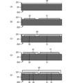
- FIG. 1(A) is a top view of the capacitor according to the first embodiment of the present invention
- FIG. 1(B) is a diagram showing the AB cross section shown in FIG. 1(A).
- FIG. 2 is an enlarged sectional view of the vicinity of the side surface of the capacitor and the vicinity of the side surface of the terminal electrode according to the first embodiment of the present invention.
- FIG. 3 is a side sectional view showing a discharge state of static electricity in the capacitor according to the first embodiment.
- FIG. 4 is a graph showing the relationship between the dielectric breakdown of the dielectric that constitutes the capacitance, the thickness Td, and the shortest distance Tsr. 5(A), FIG. 5(B), FIG. 5(C), FIG. 5(D), and FIG.
- FIG. 5(E) show the configuration at each manufacturing process of the capacitor according to the first embodiment of the present invention.
- FIG. 6(A), FIG. 6(B), FIG. 6(C), and FIG. 6(D) are cross-sectional views showing the structure of the capacitor according to the first embodiment of the present invention at each manufacturing process.
- FIG. 7(A) is a top view of a capacitor according to the second embodiment of the present invention
- FIG. 7(B) is a diagram showing a cross section taken along line AB shown in FIG. 7(A).
- FIG. 8 is an enlarged cross-sectional view of the vicinity of the side surface of a capacitor and the vicinity of the side surface of a terminal electrode according to the second embodiment of the present invention.
- FIG. 8 is an enlarged cross-sectional view of the vicinity of the side surface of a capacitor and the vicinity of the side surface of a terminal electrode according to the second embodiment of the present invention.
- FIG. 10(A) is a top view of a capacitor according to a fourth embodiment of the present invention
- FIG. 10(B) is a diagram showing a cross section taken along line AB shown in FIG. 10(A).
- FIG. 11 is a diagram showing a cross section of a capacitor according to a fifth embodiment of the present invention.
- FIG. 12 is a diagram showing a cross section of a capacitor according to a sixth embodiment of the present invention.
- FIG. 13 is a diagram showing a cross section of a capacitor according to a seventh embodiment of the present invention.
- FIG. 1(A) is a top view of the capacitor according to the first embodiment of the present invention
- FIG. 1(B) is a diagram showing the AB cross section shown in FIG. 1(A).
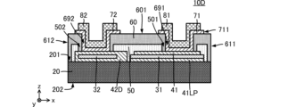
- FIG. 2 is an enlarged sectional view of the vicinity of the side surface of the capacitor and the vicinity of the side surface of the terminal electrode according to the first embodiment of the present invention. Note that in the drawings showing the configuration of each embodiment of the present invention, including FIGS. 1(A), 1(B), and 2, dimensions are exaggerated to make the technology and configuration easier to understand. It is written as follows. In particular, the dimensions in the z-axis direction are exaggerated.
- the capacitor 10 includes a substrate 20, a dielectric 31, a dielectric 32, an electrode 41, an electrode 42, a protective film 50, an insulating film 60, and a terminal electrode.
- a base electrode 71 for terminal electrodes, a base electrode 72 for terminal electrodes, an external connection electrode 81, and an external connection electrode 82 are provided.
- the substrate 20 is a flat plate and has an upper surface 201 and a lower surface 202.
- the thickness of the substrate 20 is, for example, about 150 ⁇ m.
- the substrate 20 is a conductive semiconductor, and is made of, for example, Si.
- the resistivity of the substrate 20 is, for example, 10 m ⁇ cm, and may be about 1 ⁇ cm.
- the substrate 20 corresponds to an example of the "lower electrode" of the present invention.
- the dielectric 31 and the dielectric 32 are arranged on the upper surface 201 of the substrate 20.
- the dielectric 31 and the dielectric 32 are, for example, flat films, and have a rectangular shape when viewed from above (when viewed in a direction parallel to the z-axis direction).
- Dielectric 31 and dielectric 32 are spaced apart from each other on top surface 201 .
- the dielectric 31 and the dielectric 32 are spaced apart from each other in the x-axis direction of the substrate 20.
- the thickness of the dielectric 31 and the dielectric 32 is, for example, 1.0 ⁇ m.
- Dielectric 31 and dielectric 32 are made of, for example, SiO 2 .
- the thickness and material of the dielectric 31 and the thickness and material of the dielectric 32 do not have to be the same, but if they are the same, manufacturing becomes easier and the height of the external connection electrode 81 and the external connection electrode 82 can be reduced. It will be easier to implement all together.
- the electrode 41 is placed on the top surface of the dielectric 31. More specifically, the electrode 41 is arranged on the surface of the dielectric 31 that faces the surface that the substrate 20 comes into contact with. That is, the electrode 41 and the substrate 20 are arranged with the dielectric 31 interposed therebetween.
- capacitance is generated due to the structure in which the electrode 41 and the conductive substrate 20 sandwich the dielectric 31, and this capacitance is determined by the opposing area of the electrode 41 and the substrate 20, the dielectric constant of the dielectric 31, and the dielectric It is determined by the thickness of the body 31.
- the thickness of the electrode 41 is, for example, 1.0 ⁇ m.
- the electrode 41 is made of Al, for example.
- the electrode 42 covers the dielectric 32 together with the substrate 20. Specifically, electrodes 42 are disposed on the top surface and each side of dielectric 32 to electrically and physically connect to substrate 20 . Electrode 42 is not directly physically connected to electrode 41.
- the thickness of the electrode 42 is, for example, 1.0 ⁇ m.
- the electrode 42 is made of Al, for example.
- the protective film 50 is arranged on the upper surface side of the substrate 20.
- the protective film 50 covers the upper surface 201 of the substrate 20, the dielectric 31, the electrodes 41, and the electrodes 42.
- the protective film 50 has a recess 501 that exposes a part of the upper surface of the electrode 41 and a recess 502 that exposes a part of the upper surface of the electrode 42.
- the thickness of the protective film 50 is, for example, 0.8 ⁇ m.
- the protective film 50 is made of, for example, SiN.
- the protective film 50 is a so-called passivation layer.
- the insulating film 60 covers the upper surface 201 of the substrate 20 and the protective film 50. At this time, the insulating film 60 has a recess 691 that is enclosed in the recess 501 of the protective film 50 and exposes the upper surface of the electrode 41 near the bottom, and a recess 691 that is enclosed in the recess 502 of the protective film 50 and exposes the upper surface of the electrode 42 near the bottom. It has a recess 692. That is, the insulating film 60 covers the electrode 41, the electrode 42, the dielectric 31, the dielectric 32, a portion of a terminal electrode (described later) excluding an external connection portion, and a portion of the substrate 20 (upper surface 201).
- the thickness of the insulating film 60 is, for example, 5.0 ⁇ m.
- the insulating film 60 is, for example, an organic film made of a predetermined structure and having insulating properties.
- the insulating film 60 is a so-called solder resist layer.
- the base electrode 71 for the terminal electrode is arranged on the upper surface 601 of the insulating film 60, the inner surface of the recess 691, and the surface exposed by the recess 691 in the electrode 41.
- the base electrode 71 has a rectangular shape when viewed from above.
- the base electrode 71 is, for example, an electrode layer in which Ti and Cu are sequentially formed by sputtering, and the thickness of Ti is 0.1 ⁇ m and the thickness of Cu is 1.0 ⁇ m.
- the external connection electrode 81 covers the upper surface of the base electrode 71.
- the external connection electrode 81 is, for example, a plating layer in which Ni and Au are sequentially formed, and the thickness of Ni is 3.0 ⁇ m and the thickness of Au is 0.1 ⁇ m.
- These base electrode 71 and external connection electrode 81 constitute the "terminal electrode” (terminal electrode for upper electrode) of the present invention.
- the base electrode 72 is arranged on the base electrode 72 for the terminal electrode, the upper surface 601 of the insulating film 60, the inner surface of the recess 692, and the surface exposed by the recess 692 in the electrode 42.
- the base electrode 72 has a rectangular shape when viewed from above.
- the base electrode 72 is, for example, an electrode layer in which Ti and Cu are sequentially formed by sputtering, and the thickness of Ti is 0.1 ⁇ m and the thickness of Cu is 1.0 ⁇ m.
- the external connection electrode 82 covers the upper surface of the base electrode 72.
- the external connection electrode 82 is, for example, a plating layer in which Ni and Au are sequentially formed, and the thickness of Ni is 3.0 ⁇ m and the thickness of Au is 0.1 ⁇ m.
- These base electrode 72 and external connection electrode 82 constitute a terminal electrode, more specifically, a "terminal electrode for lower electrode” of the present invention.
- the base electrode 71 and the base electrode 72 and the terminal electrode 81 and the terminal electrode 82 are schematically shown as rectangles. However, the corners may be rounded, or the portions corresponding to the corners may be formed at an angle greater than 90 degrees by chamfering.
- the capacitor 10 realizes a capacitor (MIM capacitor) formed by thin film technology.
- the side surface 711 of the base electrode 71 for a terminal electrode is in contact with the upper surface 601 of the insulating film 60, and is arranged near the side surface 611 of the insulating film 60.
- the distance between the side surface 711 and the side surface 611 of the insulating film 60 is assumed to be D761. More specifically, the distance D761 is the shortest distance between the side surfaces 711 and the side surfaces 611 along the upper surface 601 of the insulating film 60.
- the thickness of the insulator is T611. More specifically, the thickness T611 is the shortest distance from the point where the straight line forming the distance D761 touches the side surface 611 to the side surface of the substrate 20 along the side surface 611 in the thickness direction (z-axis direction) of the insulating film 60. be.
- the thickness of the dielectric 31 is assumed to be Td.
- the shortest distance Tsr and the thickness Td satisfy the following relationship.
- the dielectric thickness Td is approximately 1.0 ⁇ m
- the distance D761 is approximately 8 ⁇ m
- the thickness T611 is approximately 8 ⁇ m.
- FIG. 3 is a side cross-sectional view showing a state of static electricity discharge in the capacitor according to the first embodiment.
- ESD static electricity
- Equation 1 the voltage generated by the static electricity will be discharged in the air through the path (air path) passing through the surface of the insulating film 60 faster than the voltage generated by the static electricity reaches the dielectric breakdown voltage of the dielectric 31. As a result, static electricity charges flow to the substrate 20.
- the substrate 20 is electrically connected to a lower electrode terminal electrode (external connection electrode 82 and base electrode 72) connected to an external ground potential through the electrode 42. Therefore, the charges flowing into the substrate 20 are discharged to the ground through the electrode 42 and the lower electrode terminal electrode.
- FIG. 4 is a graph showing the relationship between the dielectric breakdown of the dielectric that constitutes the capacitance, the thickness Td, and the shortest distance Tsr.
- the solid line indicates a curve (function) in which the inequality sign in (Formula 1) is replaced with an equality sign.
- FIG. 4 shows the dielectric breakdown state of the dielectric when 1 kV of static electricity of the HBM is applied to the terminal electrode, where OK means no dielectric breakdown and NG means dielectric breakdown.
- the capacitor 10 can suppress dielectric breakdown of the dielectric 31.
- the capacitor 10 does not separately provide a functional element for discharging unlike the conventional technology. Thereby, the capacitor 10 can suppress dielectric breakdown of the dielectric 31 with a simple configuration. Further, the capacitor 10 can be made thinner and smaller than the conventional structure in which a discharge functional element is separately provided.
- Figure 5(A), Figure 5(B), Figure 5(C), Figure 5(D), Figure 5(E), Figure 6(A), Figure 6(B), Figure 6(C), Figure 6 (D) is a cross-sectional view showing the structure of the capacitor according to the first embodiment of the present invention at each manufacturing process.
- the illumination of the parts specifically shown in the explanation of the above-mentioned configuration will be omitted, and only the points that require new explanation will be explained.
- the substrate 20 is loaded, and the dielectric 30 is formed on the upper surface 201 of the substrate 20, as shown in FIG. 5(A).
- SiO 2 may be formed as a thermal oxide film on a Si substrate, or an SiO 2 or SiN film may be formed by CVD (Chemical Vapor Deposition).
- the dielectric 30 is pattern-etched to form a dielectric 31 and a dielectric 32, as shown in FIG. 5(B).
- an electrode 40 is formed on the upper surface 201 side of the substrate 20 so as to cover the dielectric 31 and the dielectric 32.
- a metal such as Al or Cu may be formed using a vapor deposition method, a sputtering method, a plating method, or the like.
- the electrode 40 is pattern-etched to form an electrode 41 and an electrode 42, as shown in FIG. 5(D).
- a protective film 50 (passivation film) is formed on the upper surface 201 side of the substrate 20 so as to cover the dielectric 31, the electrode 41, and the electrode 42.
- the protective film may be formed of SiO 2 or SiN using CVD or spin coating.
- the protective film 50 is pattern-etched to form a recess 501 that exposes a portion of the upper surface of the electrode 41 and a recess 502 that exposes a portion of the upper surface of the electrode 42 as shown in FIG. 6(A). 50.
- an insulating film 60 is formed to cover the protective film 50.
- the insulating film 60 has a recess 691 and a recess 692.
- the power supply film 70 is formed to cover the upper surface 601 of the insulating film 60, the wall surfaces of the recess 691, and the wall surfaces of the recess 692.
- the power supply film 70 is realized, for example, by sputtering or electroless plating.
- the external connection electrode 81 and the external connection electrode 82 are formed to include the regions of the recess 691 and the recess 692 in the power supply film 70.
- the external connection electrode 81 and the external connection electrode 82 are realized, for example, by electrolytic plating using a mask.
- the power supply film 70 is pattern-etched to form a base electrode 71 and a base electrode 72.
- the processing up to this point is performed on a motherboard on which a plurality of capacitors 10 are arranged. Thereafter, the substrate 20 is appropriately ground from the lower surface 202 side, and the mother substrate is cut into pieces into a plurality of capacitors 10.
- FIG. 7(A) is a top view of a capacitor according to the second embodiment of the present invention
- FIG. 7(B) is a diagram showing a cross section taken along line AB shown in FIG. 7(A).
- FIG. 8 is an enlarged cross-sectional view of the vicinity of the side surface of a capacitor and the vicinity of the side surface of a terminal electrode according to the second embodiment of the present invention.
- the capacitor 10A according to the second embodiment has terminal electrodes (base electrode 71A, The difference is in the configuration of the external connection electrode 81A).
- the other configuration of the capacitor 10A is the same as that of the capacitor 10, and a description of the similar parts will be omitted.
- the base electrode 71A is rectangular when viewed from above, and includes a side surface 711, a side surface 712, a side surface 713, and a side surface 714.
- the side surface 711 is close to and parallel to the side surface 611 of the insulating film 60 .
- the side surface 712 faces the side surface 711 and is the side surface of the base electrode 71A on the base electrode 72 side.
- the side surface 713 is close to and parallel to the side surface 613 of the insulating film 60.
- the side surface 714 faces the side surface 713 and is close to and parallel to the side surface 614 of the insulating film 60. Note that parallel here is not limited to perfect parallel, but also includes within the range of manufacturing error.
- the base electrode 71A includes a main portion, a protrusion 791, a protrusion 793, and a protrusion 794.
- the main portion of the base electrode 71A is the above-mentioned rectangular portion when viewed from above.
- the protruding portion 791 protrudes from the side surface 711 of the main portion toward the side surface 611 of the insulating film 60 when the base electrode 71A is viewed from above. At this time, the width of the protrusion 791 is smaller than the width of the side surface 711.
- the protruding portion 793 protrudes from the side surface 713 of the main portion toward the side surface 613 of the insulating film 60 when the base electrode 71A is viewed from above. At this time, the width of the protrusion 793 is smaller than the width of the side surface 713.
- the protruding portion 794 protrudes from the side surface 714 of the main portion toward the side surface 614 of the insulating film 60 when the base electrode 71A is viewed from above. At this time, the width of the protrusion 794 is smaller than the width of the side surface 714.
- the further shortest distance becomes the shortest distance Tsr.
- the distance between the tip 7911 of the protrusion 791 and the side surface 611 of the insulating film 60 is D761A
- the shortest distance Tsr is the sum of this distance D761A and the thickness T611.
- the dielectric thickness Td is approximately 1.0 ⁇ m
- the distance D761A is approximately 3 ⁇ m
- the thickness T611 is approximately 8 ⁇ m.
- the capacitor 10A can discharge static electricity through air discharge and suppress dielectric breakdown of the dielectric 31.
- the capacitor 10A can control the position of the air discharge from the terminal electrode. Further, in the capacitor 10A, the shortest distance Tsr can be shortened without changing the position of the side surface 711 on the side surface 611 side of the insulating film 60 of the terminal electrode. Thereby, in the capacitor 10A, the terminal electrode can be made smaller while maintaining discharge performance, and the parasitic capacitance formed by the terminal electrode and the substrate 20 can be reduced.
- the shape of the tip 7911 of the protrusion 791, the shape of the tip 7931 of the protrusion 793, and the shape of the tip 7941 of the protrusion 794 are tapered. Thereby, the capacitor 10A can further control the discharge location.
- the capacitor 10A is shown as having three protrusions (a protrusion 791, a protrusion 793, and a protrusion 794).
- the number of protrusions is not limited to this, and it is sufficient that there is at least one protrusion.
- one side surface may be provided with a plurality of protrusions.
- the capacitor 10A when the capacitor 10A includes an even number of protrusions such as two, it is preferable to provide a pair of protrusions on the side surface 713 and the side surface 714. As a result, even if a misalignment occurs when cutting the capacitor 10A from the motherboard into individual pieces, either the protruding portion on the side surface 713 side or the protruding portion on the side surface 714 side will always meet the above (Formula 1). arranged to meet the requirements. Thereby, the capacitor 10A can suppress dielectric breakdown of the dielectric 31 more reliably.
- FIG. 9 is an enlarged cross-sectional view of the vicinity of the side surface of a capacitor and the vicinity of the side surface of a terminal electrode according to the third embodiment of the present invention.
- the capacitor 10B according to the third embodiment differs from the capacitor 10A according to the second embodiment in the configuration of the terminal electrodes (base electrode 71B, external connection electrode 81B).
- the other configuration of the capacitor 10B is the same as that of the capacitor 10A, and a description of the similar parts will be omitted.
- the outer shape of the external connection electrode 81B is larger than the outer shape of the base electrode 71B.
- the side surface 891B of the external connection electrode 81B on the side surface 611 of the insulating film 60 protrudes more toward the side surface 611 than the side surface 711 of the base electrode 71B on the side surface 611 of the insulating film 60.
- a gap GAP is formed between the external connection electrode 81B and the insulating film 60 in a portion of the external connection electrode 81B that protrudes beyond the base electrode 71B.
- the air gap GAP is, for example, about 0.1 ⁇ m to 2.0 ⁇ m.
- Such a gap GAP can be realized by performing selective etching in which the base electrode 71B is more easily etched than the external connection electrode 81B.
- the distance D861B between the side surface 891B of the external connection electrode 81B (for example, the tip of the protrusion of the external connection electrode 81B corresponding to the protrusion 791) and the side surface 611 of the insulating film 60 is set to the side surface 711B of the base electrode 71B. (for example, the tip of the protrusion 791) and the side surface 611 of the insulating film 60 can be made shorter than the distance.
- the shortest distance Tsr is the sum of the distance D861B and the thickness T611.
- capacitor 10B has the same effects as capacitor 10B.
- the capacitor 10B the area of the base electrode 71B disposed on the upper surface 601 of the insulating film 60 can be reduced. Thereby, the capacitor 10B can suppress the parasitic capacitance generated between the electrode 41 and the base electrode 71B.
- the side surface 711B of the base electrode 71B is farther from the side surface 611 of the insulating film 60 than the side surface of the electrode 41 on the side surface 611 of the insulating film 60 (see the broken line in FIG. 9). ), the area where the electrode 41 and the base electrode 71B face each other can be further reduced. Therefore, capacitor 10B can further suppress parasitic capacitance occurring between electrode 41 and base electrode 71B.
- the external connection electrode 81B can prevent the shortest distance Tsr from increasing, and achieve aerial discharge at a desired voltage. Further, in the region where the external connection electrode 81B and the electrode 41 face each other without interposing the base electrode 71B, a gap GAP exists, so that the capacitor 10B has a parasitic capacitance generated between the electrode 41 and the external connection electrode 81B. can be suppressed.
- FIG. 10(A) is a top view of a capacitor according to a fourth embodiment of the present invention
- FIG. 10(B) is a diagram showing a cross section taken along line AB shown in FIG. 10(A).
- a capacitor 10C according to the fourth embodiment differs from a capacitor 10A according to the second embodiment in that it includes an insulating film 90.
- the other configuration of the capacitor 10C is the same as that of the capacitor 10A, and a description of the similar parts will be omitted.
- the insulating film 90 of the capacitor 10C includes an insulating film 60, a base electrode 71C (same configuration as the base electrode 71A), a base electrode 72, an external connection electrode 81C (same configuration as the external connection electrode 81A), and an external connection electrode 82. cover.
- the insulating film 90 includes the central part of the external connection electrode 81C when viewed from above (the part used as the mounting electrode), the central part of the external connection electrode 82 when viewed from above (the part used as the mounting electrode), and the base electrode.
- a portion including the tip 7911 of the protrusion 791 of the base electrode 71C, a portion including the tip 7931 of the protrusion 793 of the base electrode 71C, and a portion including the tip 7941 of the protrusion 794 of the base electrode 71C are exposed to the outside.
- the insulating film 90 may be made of the same material as the insulating film 60 or may be a different material, but by using the same material, it can be expected that the adhesion between the insulating film 60 and the insulating film 90 will be improved. If they are formed using the same material, the boundary between the insulating film 60 and the insulating film 90 may be unclear.
- the capacitor 10C can alleviate the impact during mounting. Further, since the protruding portion of the capacitor 10C is exposed from the insulating film 90, dielectric breakdown of the dielectric 31 due to air discharge of static electricity can be suppressed similarly to the capacitor 10A. That is, the capacitor 10C has the same effect as the capacitor 10A.
- FIG. 11 is a diagram showing a cross section of a capacitor according to a fifth embodiment of the present invention.
- FIG. 11 shows an AB cross section similar to FIG. 1(A) and the like.
- a capacitor 10D according to the fifth embodiment differs from the capacitor 10 according to the first embodiment in that it includes an electrode 41LP and that it includes an electrode 42D instead of the electrode 42.
- the other configuration of the capacitor 10D is the same as that of the capacitor 10, and a description of the similar parts will be omitted.
- the electrode 41LP is arranged between the substrate 20 and the dielectric 31. Electrode 41LP is connected to substrate 20. Electrode 41LP faces electrode 41 with dielectric 31 in between.
- the electrode 41LP and the substrate 20 constitute the "lower electrode” of the present invention.
- the electrode 42D is formed by a combination of an electrode film formed at the same timing as the electrode 41LP and the electrode 42 in the capacitor 10, and covers the entire surface of the dielectric 32.
- the capacitor 10D has the same effects as the capacitor 10.
- FIG. 12 is a diagram showing a cross section of a capacitor according to a sixth embodiment of the present invention. Similar to FIG. 11, FIG. 12 shows an AB cross section similar to FIG. 1(A) and the like.
- the capacitor 10E according to the sixth embodiment differs from the capacitor 10D according to the fifth embodiment in that it includes a lower protective film 50LP, a plurality of via conductors 419, and a plurality of via conductors 429. It's different.
- the other configurations of capacitor 10E are similar to capacitor 10D, and explanations of similar parts will be omitted.
- the capacitor 10E includes a lower protective film 50LP on the upper surface 201 of the substrate 20.
- the lower protective film 50LP is made of the same material as the protective film 50, for example.
- the lower protective film 50LP is arranged between the substrate 20 and the electrode 41LP, and is arranged between the substrate 20 and the electrode 42E (same configuration as the electrode 42D).
- the plurality of via conductors 419 are formed in the lower protective film 50LP and penetrate the lower protective film 50LP in the thickness direction.
- the plurality of via conductors 419 connect the substrate 20 and the electrode 41LP for electrical conduction.
- a plurality of via conductors 429 are formed in the lower protective film 50LP and penetrate the lower protective film 50LP in the thickness direction.
- the plurality of via conductors 429 connect the substrate 20 and the electrode 42E for electrical conduction.
- the capacitor 10E has the same effects as the capacitor 10D.
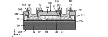
- FIG. 13 is a diagram showing a cross section of a capacitor according to a seventh embodiment of the present invention.
- FIG. 13 shows an AB cross section similar to FIG. 1(A) and the like.
- a capacitor 10F according to the seventh embodiment differs from the capacitor 10 according to the first embodiment in that it includes an electrode 20e and a substrate 20i instead of the substrate 20.
- the other configuration of the capacitor 10F is the same as that of the capacitor 10, and a description of the similar parts will be omitted.
- the substrate 20i is an insulating substrate.
- the substrate 20i is made of alumina, for example.
- the electrode 20e is arranged on the upper surface 201 of the substrate 20i.
- the electrode 20e has conductivity.
- the lower electrode is thus realized by the electrode 20e placed on the insulating substrate 20i.
- the dielectric 31 and the dielectric 32 are arranged on the upper surface of the electrode 20e (the surface facing the surface that contacts the substrate 20i).
- T611 is not the distance from the substrate but the distance from the electrode 20e.
- the capacitor 10F has the same effects as the capacitor 10.
- the shape of the insulating film 60 is shown as a rectangle when viewed from the Y-axis direction, but it does not necessarily have to be a rectangle, and may have a shape in which the base electrode or connection terminal electrode is connected to the substrate by a straight line, A shape connected by a curved line may also be used. Regardless of the shape, it is sufficient that the shortest distance passing through the surface of the insulating film 60 from the base electrode or the connection terminal electrode to the substrate on which each functional film is not formed is Tsr, and formula 1 is satisfied.
- the side surface 611 of the insulating film 60 is integrated with the side surface of the substrate, but the substrate 20 may protrude from the capacitor formation portion when viewed from the Z-axis direction. In that case, the distance between a point on the upper surface 201 of the substrate 20 and the end of the base electrode or the connecting terminal electrode becomes the shortest distance Tsr.
- the terminal electrode includes a protrusion that protrudes from a side surface of a main portion having a predetermined shape when viewed from above,
- the protruding portion includes a plurality of protruding portions arranged at opposing positions with the main portion interposed therebetween.
- the terminal electrode is a base electrode electrically connected to the upper electrode; an external connection electrode formed on the base electrode; Equipped with The base electrode and the external connection electrode have a portion facing the upper electrode, The external connection electrode protrudes from the base electrode,
- the capacitor according to any one of ⁇ 1> to ⁇ 3>, wherein a gap is provided between the external connection electrode and the upper electrode in a portion where the external connection electrode protrudes beyond the base electrode.
- ⁇ 6> The capacitor according to any one of ⁇ 1> to ⁇ 5>, wherein the lower electrode is a conductive semiconductor substrate.
- ⁇ 7> The capacitor according to ⁇ 6>, wherein the lower electrode includes a conductive film disposed between a conductive semiconductor substrate and the dielectric.
- the lower electrode is an insulating substrate, a conductive film disposed between the insulating substrate and the dielectric;
- the terminal electrode is electrically connected to the upper electrode
Landscapes
- Engineering & Computer Science (AREA)
- Power Engineering (AREA)
- Microelectronics & Electronic Packaging (AREA)
- Manufacturing & Machinery (AREA)
- Chemical & Material Sciences (AREA)
- Materials Engineering (AREA)
- Fixed Capacitors And Capacitor Manufacturing Machines (AREA)
Priority Applications (3)
| Application Number | Priority Date | Filing Date | Title |
|---|---|---|---|
| CN202380052136.4A CN119497900A (zh) | 2022-07-13 | 2023-07-04 | 电容器 |
| JP2024533656A JP7768388B2 (ja) | 2022-07-13 | 2023-07-04 | キャパシタ |
| US19/009,406 US20250140472A1 (en) | 2022-07-13 | 2025-01-03 | Capacitor |
Applications Claiming Priority (2)
| Application Number | Priority Date | Filing Date | Title |
|---|---|---|---|
| JP2022-112345 | 2022-07-13 | ||
| JP2022112345 | 2022-07-13 |
Related Child Applications (1)
| Application Number | Title | Priority Date | Filing Date |
|---|---|---|---|
| US19/009,406 Continuation US20250140472A1 (en) | 2022-07-13 | 2025-01-03 | Capacitor |
Publications (1)
| Publication Number | Publication Date |
|---|---|
| WO2024014351A1 true WO2024014351A1 (ja) | 2024-01-18 |
Family
ID=89536575
Family Applications (1)
| Application Number | Title | Priority Date | Filing Date |
|---|---|---|---|
| PCT/JP2023/024716 Ceased WO2024014351A1 (ja) | 2022-07-13 | 2023-07-04 | キャパシタ |
Country Status (4)
| Country | Link |
|---|---|
| US (1) | US20250140472A1 (https=) |
| JP (1) | JP7768388B2 (https=) |
| CN (1) | CN119497900A (https=) |
| WO (1) | WO2024014351A1 (https=) |
Citations (2)
| Publication number | Priority date | Publication date | Assignee | Title |
|---|---|---|---|---|
| JP2021093439A (ja) * | 2019-12-10 | 2021-06-17 | 株式会社村田製作所 | 半導体装置 |
| WO2021149688A1 (ja) * | 2020-01-20 | 2021-07-29 | 株式会社村田製作所 | 半導体装置及び容量装置 |
-
2023
- 2023-07-04 WO PCT/JP2023/024716 patent/WO2024014351A1/ja not_active Ceased
- 2023-07-04 CN CN202380052136.4A patent/CN119497900A/zh active Pending
- 2023-07-04 JP JP2024533656A patent/JP7768388B2/ja active Active
-
2025
- 2025-01-03 US US19/009,406 patent/US20250140472A1/en active Pending
Patent Citations (2)
| Publication number | Priority date | Publication date | Assignee | Title |
|---|---|---|---|---|
| JP2021093439A (ja) * | 2019-12-10 | 2021-06-17 | 株式会社村田製作所 | 半導体装置 |
| WO2021149688A1 (ja) * | 2020-01-20 | 2021-07-29 | 株式会社村田製作所 | 半導体装置及び容量装置 |
Also Published As
| Publication number | Publication date |
|---|---|
| US20250140472A1 (en) | 2025-05-01 |
| JP7768388B2 (ja) | 2025-11-12 |
| JPWO2024014351A1 (https=) | 2024-01-18 |
| CN119497900A (zh) | 2025-02-21 |
Similar Documents
| Publication | Publication Date | Title |
|---|---|---|
| US12288646B2 (en) | Capacitor with connection conductor contacting a surface of a substrate | |
| US7154158B2 (en) | Semiconductor device having MIM structure resistor | |
| CN102760553B (zh) | 片式线圈元件 | |
| US11158456B2 (en) | Trench capacitor | |
| US20120300355A1 (en) | Electrostatic protection component | |
| US20090109596A1 (en) | Multilayer capacitor | |
| JP5710708B2 (ja) | 積層セラミックキャパシタ及び積層セラミックキャパシタの実装基板 | |
| US11521800B2 (en) | Capacitor | |
| JP2017195321A (ja) | チップコンデンサ | |
| JP7768388B2 (ja) | キャパシタ | |
| JP7420230B2 (ja) | 半導体装置及びモジュール | |
| US11545304B2 (en) | Capacitor cluster having capacitors with different shapes | |
| CN117638654A (zh) | 瞬态电压保护器件 | |
| US20250218680A1 (en) | Capacitor | |
| TWI871180B (zh) | 電阻器及其製造方法 | |
| US20250210269A1 (en) | Capacitor | |
| CN120452964A (zh) | 电阻器及其制造方法 | |
| JP7042967B2 (ja) | 半導体装置 | |
| JP2013182755A (ja) | 静電気保護素子 | |
| CN118974862A (zh) | 电子部件 | |
| JP2017195320A (ja) | チップコンデンサ | |
| JP2007251203A (ja) | Mim構造抵抗体を搭載した半導体装置 |
Legal Events
| Date | Code | Title | Description |
|---|---|---|---|
| 121 | Ep: the epo has been informed by wipo that ep was designated in this application |
Ref document number: 23839523 Country of ref document: EP Kind code of ref document: A1 |
|
| WWE | Wipo information: entry into national phase |
Ref document number: 2024533656 Country of ref document: JP |
|
| WWE | Wipo information: entry into national phase |
Ref document number: 202380052136.4 Country of ref document: CN |
|
| NENP | Non-entry into the national phase |
Ref country code: DE |
|
| WWP | Wipo information: published in national office |
Ref document number: 202380052136.4 Country of ref document: CN |
|
| 122 | Ep: pct application non-entry in european phase |
Ref document number: 23839523 Country of ref document: EP Kind code of ref document: A1 |