WO2024014192A1 - アニオン含有無機固体材料およびアニオン含有無機固体材料の製造方法 - Google Patents
アニオン含有無機固体材料およびアニオン含有無機固体材料の製造方法 Download PDFInfo
- Publication number
- WO2024014192A1 WO2024014192A1 PCT/JP2023/021178 JP2023021178W WO2024014192A1 WO 2024014192 A1 WO2024014192 A1 WO 2024014192A1 JP 2023021178 W JP2023021178 W JP 2023021178W WO 2024014192 A1 WO2024014192 A1 WO 2024014192A1
- Authority
- WO
- WIPO (PCT)
- Prior art keywords
- anion
- doped
- containing inorganic
- inorganic solid
- doping
- Prior art date
- Legal status (The legal status is an assumption and is not a legal conclusion. Google has not performed a legal analysis and makes no representation as to the accuracy of the status listed.)
- Ceased
Links
Images





Classifications
-
- C—CHEMISTRY; METALLURGY
- C01—INORGANIC CHEMISTRY
- C01G—COMPOUNDS CONTAINING METALS NOT COVERED BY SUBCLASSES C01D OR C01F
- C01G51/00—Compounds of cobalt
-
- C—CHEMISTRY; METALLURGY
- C04—CEMENTS; CONCRETE; ARTIFICIAL STONE; CERAMICS; REFRACTORIES
- C04B—LIME, MAGNESIA; SLAG; CEMENTS; COMPOSITIONS THEREOF, e.g. MORTARS, CONCRETE OR LIKE BUILDING MATERIALS; ARTIFICIAL STONE; CERAMICS; REFRACTORIES; TREATMENT OF NATURAL STONE
- C04B35/00—Shaped ceramic products characterised by their composition; Ceramics compositions; Processing powders of inorganic compounds preparatory to the manufacturing of ceramic products
- C04B35/50—Shaped ceramic products characterised by their composition; Ceramics compositions; Processing powders of inorganic compounds preparatory to the manufacturing of ceramic products based on rare-earth compounds
-
- C—CHEMISTRY; METALLURGY
- C04—CEMENTS; CONCRETE; ARTIFICIAL STONE; CERAMICS; REFRACTORIES
- C04B—LIME, MAGNESIA; SLAG; CEMENTS; COMPOSITIONS THEREOF, e.g. MORTARS, CONCRETE OR LIKE BUILDING MATERIALS; ARTIFICIAL STONE; CERAMICS; REFRACTORIES; TREATMENT OF NATURAL STONE
- C04B41/00—After-treatment of mortars, concrete, artificial stone or ceramics; Treatment of natural stone
- C04B41/80—After-treatment of mortars, concrete, artificial stone or ceramics; Treatment of natural stone of only ceramics
-
- C—CHEMISTRY; METALLURGY
- C30—CRYSTAL GROWTH
- C30B—SINGLE-CRYSTAL GROWTH; UNIDIRECTIONAL SOLIDIFICATION OF EUTECTIC MATERIAL OR UNIDIRECTIONAL DEMIXING OF EUTECTOID MATERIAL; REFINING BY ZONE-MELTING OF MATERIAL; PRODUCTION OF A HOMOGENEOUS POLYCRYSTALLINE MATERIAL WITH DEFINED STRUCTURE; SINGLE CRYSTALS OR HOMOGENEOUS POLYCRYSTALLINE MATERIAL WITH DEFINED STRUCTURE; AFTER-TREATMENT OF SINGLE CRYSTALS OR A HOMOGENEOUS POLYCRYSTALLINE MATERIAL WITH DEFINED STRUCTURE; APPARATUS THEREFOR
- C30B31/00—Diffusion or doping processes for single crystals or homogeneous polycrystalline material with defined structure; Apparatus therefor
- C30B31/20—Doping by irradiation with electromagnetic waves or by particle radiation
- C30B31/22—Doping by irradiation with electromagnetic waves or by particle radiation by ion-implantation
-
- C—CHEMISTRY; METALLURGY
- C30—CRYSTAL GROWTH
- C30B—SINGLE-CRYSTAL GROWTH; UNIDIRECTIONAL SOLIDIFICATION OF EUTECTIC MATERIAL OR UNIDIRECTIONAL DEMIXING OF EUTECTOID MATERIAL; REFINING BY ZONE-MELTING OF MATERIAL; PRODUCTION OF A HOMOGENEOUS POLYCRYSTALLINE MATERIAL WITH DEFINED STRUCTURE; SINGLE CRYSTALS OR HOMOGENEOUS POLYCRYSTALLINE MATERIAL WITH DEFINED STRUCTURE; AFTER-TREATMENT OF SINGLE CRYSTALS OR A HOMOGENEOUS POLYCRYSTALLINE MATERIAL WITH DEFINED STRUCTURE; APPARATUS THEREFOR
- C30B33/00—After-treatment of single crystals or homogeneous polycrystalline material with defined structure
- C30B33/04—After-treatment of single crystals or homogeneous polycrystalline material with defined structure using electric or magnetic fields or particle radiation
-
- H—ELECTRICITY
- H01—ELECTRIC ELEMENTS
- H01M—PROCESSES OR MEANS, e.g. BATTERIES, FOR THE DIRECT CONVERSION OF CHEMICAL ENERGY INTO ELECTRICAL ENERGY
- H01M4/00—Electrodes
- H01M4/02—Electrodes composed of, or comprising, active material
- H01M4/36—Selection of substances as active materials, active masses, active liquids
- H01M4/58—Selection of substances as active materials, active masses, active liquids of inorganic compounds other than oxides or hydroxides, e.g. sulfides, selenides, tellurides, halogenides or LiCoFy; of polyanionic structures, e.g. phosphates, silicates or borates
-
- Y—GENERAL TAGGING OF NEW TECHNOLOGICAL DEVELOPMENTS; GENERAL TAGGING OF CROSS-SECTIONAL TECHNOLOGIES SPANNING OVER SEVERAL SECTIONS OF THE IPC; TECHNICAL SUBJECTS COVERED BY FORMER USPC CROSS-REFERENCE ART COLLECTIONS [XRACs] AND DIGESTS
- Y02—TECHNOLOGIES OR APPLICATIONS FOR MITIGATION OR ADAPTATION AGAINST CLIMATE CHANGE
- Y02E—REDUCTION OF GREENHOUSE GAS [GHG] EMISSIONS, RELATED TO ENERGY GENERATION, TRANSMISSION OR DISTRIBUTION
- Y02E60/00—Enabling technologies; Technologies with a potential or indirect contribution to GHG emissions mitigation
- Y02E60/30—Hydrogen technology
- Y02E60/50—Fuel cells
Definitions
- the present invention relates to an anion-containing inorganic solid material and a method for producing an anion-containing inorganic solid material.
- Patent Document 1 in order to dope the sintered ceramic as an inorganic solid material with ions, a solid electrolyte and a current collector are installed on the sintered ceramic, and the ceramic current collector is A method is disclosed in which a current is passed between the two.
- the inorganic solid material to be doped can be doped with metal cations from the solid electrolyte layer on the anode side and anions from the solid electrolyte layer on the cathode side. It is said that
- inorganic solid materials may have different characteristics such as catalytic activity depending on their crystallinity, and there is a need for inorganic solid materials that exhibit novel configurations in terms of crystal structure.
- the present invention was made in view of the above-mentioned circumstances.
- One or more anion species are introduced in an arbitrary amount into an inorganic solid material, and a region composed of polycrystals and amorphous is formed on the surface with a predetermined thickness.
- An object of the present invention is to provide an anion-containing inorganic solid material having a novel crystal structure.
- the present invention provides the following means to solve the above problems.
- the anion-containing inorganic solid material according to one aspect of the present invention has a first region located on the outermost surface and composed of polycrystalline and amorphous materials, and a first region located inside the first region and composed of polycrystalline and amorphous materials. and a second region made of crystal.
- the average thickness of the first region from the outermost surface may be 20 nm or less.
- the anion concentration in the first region may be higher than the anion concentration in the second region.
- the anion-containing inorganic solid material of any of (1) to (3) above has the general formula (La, Sr)CoO 3- ⁇ F y (where 0 ⁇ 3, 0 ⁇ y, y ⁇ ) may be used.
- a method for producing an anion-containing inorganic solid material according to one embodiment of the present invention is a laminate in which an electrode, a solid electrolyte layer, and a layer to be doped containing a material to be doped are laminated in this order to form a laminate. a step of setting voltage application conditions such that a first region composed of polycrystals and amorphous is formed with a predetermined thickness on the surface of the laminate, and a step of setting voltage application conditions of the layer to be doped.
- the doped material a doping step of doping with an anion, in the voltage application condition setting step, adjusting the voltage applied to the laminated body, and in the doping step, adjusting the value of the current flowing with respect to 1 g of the doped material.
- a voltage is applied to the laminate so that a current value is less than 0.6 mA/g with respect to 1 g of the doped material. may be applied.
- a voltage is applied to the laminate so that a current value is 2.5 mA/g or more with respect to 1 g of the doped material. may be applied.
- the layer to be doped is formed with a mixture of the material to be doped and a soluble solid electrolyte; After the doping step, the method may further include a washing step of washing the mixture to remove the soluble solid electrolyte.
- the method for producing an anion-containing inorganic solid material according to (5) to (8) above includes, in the lamination step, a solid electrolyte layer composed of a reversible electrode containing fluorine and a solid electrolyte containing fluorine; A laminate may be formed in which La, Sr)CoO 3 are stacked in this order.
- An anion-containing inorganic material having a novel crystal structure in which an arbitrary amount of one or more anion species is introduced into an inorganic solid material, and a polycrystalline and amorphous region is formed on the surface with a predetermined thickness.
- Solid materials and anion-containing inorganic solid materials can be provided.
- FIG. 1 is a cross-sectional view schematically showing an example of the structure of an anion-containing inorganic solid material according to one embodiment of the present invention.
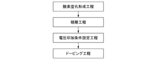
- 1 is a flowchart illustrating an example of a method for producing an anion-containing inorganic solid material according to an embodiment of the present invention.
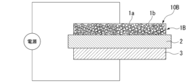
- FIG. 2 is a diagram illustrating an example of the configuration of a doping step in a method for producing an anion-containing inorganic solid material according to an embodiment of the present invention.
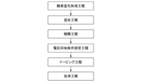
- 3 is a flowchart illustrating an example of a method for producing an anion-containing inorganic solid material according to a modification of FIG. 2.
- FIG. 4 is a diagram illustrating an example of a configuration of a doping step in a method for producing an anion-containing inorganic solid material according to a modification of FIG. 3.
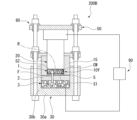
- FIG. 1 is a cross-sectional view showing an example of an anion-containing inorganic solid material manufacturing apparatus according to an embodiment of the present invention.
- 7 is a cross-sectional view showing an example of an anion-containing inorganic solid material manufacturing apparatus according to a modification of FIG. 6.
- FIG. 1 is a TEM image of a cross section of an anion-containing inorganic solid material according to Example 1.
- FIG. 9(a) is a TEM image of the cross section of the anion-containing inorganic solid material according to Example 2, and FIG.
- FIG. 9(b) is a TEM image of the area near the surface surrounded by the broken line in FIG. 9(a). It is an enlarged view.
- 3 is a TEM image of a cross section of an anion-containing inorganic solid material according to Example 3.
- 3 is a TEM image of a cross section of an anion-containing inorganic solid material according to Example 4.
- 1 is a TEM image of a cross section of an inorganic oxide according to Comparative Example 1.
- 13(a) shows the TOF-SIMS spectrum of Example 1
- FIG. 13(b) shows the TOF-SIMS spectrum of Example 2
- FIG. 13(c) shows the TOF-SIMS spectrum of Example 3.
- 13(d) shows the TOF-SIMS spectrum of Example 4, and FIG.
- 13(e) shows the TOF-SIMS spectrum of Comparative Example 1.
- 14(a) shows a diffraction spot in a region near the surface of the sample of Example 1
- FIG. 14(b) shows a diffraction spot in a region far from the surface of the sample of Example 1.
- 3 shows diffraction spots in a region away from the surface of the sample of Example 2.
- 10 shows diffraction spots in a region away from the surface of the sample of Example 3.
- 17(a) shows a diffraction spot in a region near the surface of the sample of Example 4
- FIG. 17(b) shows a diffraction spot in a region far from the surface of the sample of Example 4.
- 18(a) and 18(b) are SEM images of the outer shape of the sample of Example 1
- FIG. 18(c) and FIG. 18(d) are SEM images of the outer shape of the sample of Example 2.
- 18(e) and 18(f) are SEM images of the outer shape of the sample of Example 3
- FIG. 18(g) is the SEM image of the outer shape of the sample of Comparative Example 1. This is an SEM image.
- the powder XRD measurement results of Examples 1 to 3 and Comparative Example 1 are shown.
- the powder XRD measurement results of Example 4 and Comparative Example 1 are shown.
- FIG. 1 is a cross-sectional view schematically showing an example of the structure of an anion-containing inorganic solid material according to one embodiment of the present invention.
- the anion-containing inorganic solid material 1 according to an embodiment of the present invention is located on the outermost surface S, is located inside the first region R1 and the first region R1 composed of polycrystals and amorphous, and is composed of a single It has a second region R2 made of crystal.
- the inside represents a position spaced apart from the surface in a crystal body.
- the anion-containing inorganic solid material is, for example, a composition represented by the following general formula (1).
- the A site is a rare earth ion or an alkaline earth metal ion
- the B site is a transition metal ion
- the Z site is an anion site.
- the A site contains, for example, lanthanoids, rare earth elements such as Y having properties similar to lanthanides, and alkaline earth metals, and may be one type or multiple types.
- the rare earth element located at the A site is preferably one or more selected from the group consisting of La, Nd, Pr and Y, and preferably one or more selected from the group consisting of La, Nd and Pr. It is more preferable that there be.
- the alkaline earth metal located at the A site is preferably one or more selected from the group consisting of Ca, Sr, and Ba.
- Both rare earth elements and alkaline earth metals such as (La, Sr) may be located at the A site.
- the ratio thereof is arbitrary, for example, the molar ratio is 1:9 to 9:1, 4:6 to 6:4, etc.
- (La, Sr) represents that La and Sr are located at the A site, and the ratio thereof is arbitrary.
- one or more elements selected from the group consisting of Co, Mn, Ni, Ru, and Ir are located at the B site.
- the ratio thereof is arbitrary.
- the molar ratio B1:B2 is, for example, 1:9 to 9:1, or even 4:6 to 6:4. good.
- An anion to be doped into the material to be doped is located at the Z site.
- one or more of the halide ions are located, more specifically one or both of F ⁇ and Cl ⁇ are located.
- ⁇ satisfies 0 ⁇ 3, and y satisfies y ⁇ .
- ⁇ and y preferably satisfy 0.2 ⁇ , 0.2 ⁇ y, or 0.3 ⁇ 3, 0.3 ⁇ y ⁇ 2, and 0.4 ⁇ It is also possible to set ⁇ 3 and 0.4 ⁇ y ⁇ 3.
- either the La element or the Sr element may be located at the A site.
- the sum of the amounts of the A elements is equivalent to the amount of the B elements.
- the anion-containing inorganic solid material according to the present embodiment is formed, for example, by doping an inorganic solid material represented by the composition formula ABO3 with fluoride ions as anions.
- the inorganic solid material represented by the general formula ABO3 has a perovskite crystal structure.
- the anion-containing inorganic solid material according to this embodiment also has the same crystal structure as the inorganic solid material before doping. That is, the anion-containing inorganic solid material according to this embodiment has a perovskite crystal structure.
- the first region R1 is composed of a composition represented by the above formula (1).
- the composition of the first region R1 has a perovskite crystal structure.
- the first region R1 is made of polycrystalline and amorphous materials. Specifically, in the first region, a plurality of amorphous regions are surrounded by polycrystalline regions.
- the average thickness of the first region R1 from the outermost surface S is controlled by the current value of the laminate relative to the weight of the material to be doped during the manufacturing process, and is, for example, 2 nm or more and 20 nm or less.
- the first region R1 is composed of polycrystalline and amorphous materials. Specifically, the first region R1 is composed of an amorphous composition represented by the above formula (1) and a polycrystalline composition represented by the above formula (1).
- the first region R1 is configured, for example, in a cross-sectional view along the stacking direction, so that polycrystals surround an amorphous material provided in an island-like structure. That is, the first region R1 has a plurality of island-like structures made of amorphous material and polycrystals provided so as to surround the plurality of island-like amorphous materials. Since the first region R1 has a different crystallinity from the second region R2 and the doped material that is the base material, it may also be referred to as an altered layer.
- the first region R1 has a sufficient thickness, it has the above-mentioned crystal structure. Therefore, an annular diffraction image is observed in the electron beam diffraction image, and a contrast difference due to the difference in the crystal structure occurs in the TEM image. Some areas are sparsely confirmed.
- the second region R2 is located inside the first region R1, that is, located further away from the outermost surface S than the first region R1, and is composed of a single crystal of the composition represented by the above formula (1). ing.
- the anion concentration is configured to decrease as it moves away from the outermost surface S, for example.
- the anion concentration in the first region R1 is higher than the anion concentration in the second region R2.
- the average value of the anion concentration in the first region R1 is, for example, twice or more, and may be ten times or more, the average value of the anion concentration in the second region R2.
- FIG. 2 is a flowchart illustrating an example of a method for producing an anion-containing inorganic solid material according to an embodiment of the present invention.
- FIG. 3 is a diagram for explaining the doping process in FIG. 2.
- a method for manufacturing an anion-containing inorganic solid material includes a lamination step of forming a laminate in which an electrode, a solid electrolyte layer, and a layer to be doped containing a material to be doped are laminated in this order;
- a voltage application condition setting step of setting a voltage application condition such that a first region R1 composed of polycrystalline and amorphous materials is formed with a predetermined thickness on the surface of the laminate, and a voltage application condition setting step in which the potential of the layer to be doped is
- a doping step includes applying a voltage to the laminate under the voltage application conditions set in the voltage application condition setting step so that the potential is higher than the voltage application condition setting step, and doping the material to be doped with an anion using the doping target layer as a reaction field.
- the voltage applied to the laminate is adjusted, and in the doping step, a current flows with respect to 1 g of the doped material. Adjust values.
- the method for producing an anion-containing inorganic solid material according to an embodiment of the present invention may be performed without departing from the gist of the present invention, without departing from the spirit of the present invention.
- the process may include the following steps.
- a metal oxide having a perovskite crystal structure is typically used as the material to be doped, although it is not particularly limited.
- a metal oxide with a perovskite structure has the composition formula ABO 3- ⁇ (in the composition formula, A site: one or both of rare earth ion and alkaline earth metal ion, B site: transition metal ion, ⁇ : oxygen vacancy). amount). Note that multiple types of ions may be located at each of the A site and the B site.
- the rare earth element located at the A site is preferably one or more selected from the group consisting of La, Nd, Pr and Y, and preferably one or more selected from the group consisting of La, Nd and Pr. It is more preferable that there be.
- the alkaline earth metal located at the A site is preferably one or more selected from the group consisting of Ca, Sr, and Ba. Examples of such perovskite oxides include (La, Sr) (Co, Mn) O 3- ⁇ , (La, Sr) (Co, Ni) O 3- ⁇ , (La, Sr) (Mn, Ni )O 3- ⁇ , (Nd,Ca)(Ru,Ir)O 3- ⁇ , and the like.
- both a rare earth element such as (La, Sr) and an alkaline earth metal may be located at the A site.
- the ratio thereof is arbitrary, for example, the molar ratio is 1:9 to 9:1, 4:6 to 6:4, etc.
- (La, Sr) represents that La and Sr are located at the A site, and the ratio thereof is arbitrary.
- one or more elements selected from the group consisting of Co, Mn, Ni, Ru, and Ir are located at the B site.
- the ratio thereof is arbitrary.
- the molar ratio B1:B2 is, for example, 1:9 to 9:1, or even 4:6 to 6:4. good.
- an oxide having a perovskite crystal structure represented by the composition formula ABO 3 (in the composition formula, A and B are metal elements, and each may be composed of a plurality of metal elements).
- perovskite oxide will be described as an example.
- the present embodiment is not limited to this example, and the metal oxide having any crystal structure selected from perovskite structure, layered perovskite structure, layered rock salt type structure, and spinel type structure is used as the doped material. May be used.
- the anion species to be doped into the material to be doped is not particularly limited, but includes, for example, one or more halide ions, such as fluoride ions and chloride ions.
- an inorganic oxide used as a doped material is heated and cooled in an inert gas atmosphere to form oxygen vacancies in the doped material.
- an inorganic oxide as a material to be doped is introduced into a closed space, and heated and cooled in an atmosphere of an inert gas such as argon.
- the temperature at which the inorganic oxide is heated is, for example, 200 to 1200° C.
- the time at which the inorganic oxide is heated is, for example, 10 hours or more.
- the temperature at which the inorganic oxide is heated is, for example, 200 to 1200° C., and the time at which the inorganic oxide is heated is, for example, 10 hours or more.
- the inorganic oxide is cooled to, for example, room temperature.
- oxygen vacancies can be formed in the inorganic solid material as the material to be doped.
- the composition of the doped material becomes ABO 3- ⁇ ( ⁇ : a number less than 3) after the oxygen vacancy formation step.
- the reversible electrode 3, the solid electrolyte layer 2, and the doping target layer 1A containing the doped material 1a are each prepared as molded bodies, and these are laminated to form the laminated body 10A.
- a housing section is prepared, which is open at one end and includes a bottom wall and a side wall that stands up from the bottom wall.
- a metal film is placed on the bottom wall of the accommodating part, and the powder to be the material of the reversible electrode 3 is stored on the metal film, and is pressed in the press part to form the reversible electrode 3 as a powder compact.
- solid electrolyte pellets made of solid electrolyte are placed so as to overlap with the reversible electrode 3 to form the solid electrolyte layer 2.
- a powder containing the material to be doped 1a is stored in the storage part so as to overlap with the solid electrolyte layer 2, and the powder containing the material to be doped 1a is pressed, thereby forming the layer 1A to be doped as a green compact on the solid electrolyte layer 2.
- the mass of the doped material 1a is weighed before it is included in the laminate.
- the doping target layer 1A made of the doped material 1a may be referred to as a pellet cell.
- the above-mentioned perovskite oxide can be used as the doped material of the doping target layer 1A to form the laminated body 10A.
- a pellet cell containing the material to be doped can be used as the layer 1A to be doped.
- the pellet cell consists of a single phase of perovskite oxide.
- This pellet cell is formed, for example, by pressing solid electrolyte pellets. Thereby, the yield of the anion-containing inorganic solid material can be increased while suppressing the contamination of foreign matter into the anion-containing inorganic solid material.
- a laminate can be formed using a halide as the solid electrolyte layer 2.
- solid electrolytes include Ba 0.99 K 0.01 F 1.99 , La 0.9 Ba 0.1 F 2.9 , BaF 2 , LaF 3 , Ce 0.9 Sr 0.1 F 2. 9 , PbSnF 4 , PbF 2 , SrCl 2 , BaCl 2 , etc. can be used.
- the laminated body 10A can be formed using the solid electrolyte layer 2 and the reversible electrode 3, each containing a halide.
- the reversible electrode 3 containing a halide may be a Pb-PbF 2 mixture, a Pb-PbCl 2 mixture, a Ni-NiF 2 mixture, a Ni-NiCl 2 mixture, Zn-ZnF 2 mixture, Zn-ZnCl 2 mixture, Cu-CuF 2 mixture, Cu-CuCl 2 mixture, etc. can be used.
- the solid electrolyte layer 2 and the reversible electrode 3 have the same halide ions.
- the reversible electrode 3 may be a Pb-PbF 2 mixture, a Ni-NiF 2 mixture, or a Cu-CuF 2 mixture. It is preferred to use one selected from the group consisting of a mixture of the two .
- the doped material is formed in the doping process described later.
- Oxygen sites are doped with halide ions.
- the ionic radius of halide ions is close to the ionic radius of oxygen, so from the viewpoint of obtaining an anion-containing inorganic solid material without destroying the crystal structure of the inorganic solid material, that is, with small crystal strain, halide ions as anions can be used as anions. Can be doped into doped materials.
- the solid electrolyte layer 2 when forming the stacked body 10A using the solid electrolyte layer 2 and the reversible electrode 3 containing the same halide, when the halide ions of the reversible electrode 3 move to the solid electrolyte layer 2 in the doping process described later, the solid electrolyte layer 2 The crystal structure of the composition constituting the electrolyte layer 2 becomes difficult to collapse, and the ionic conductivity in the solid electrolyte layer 2 can be further improved.
- the housing portion may be filled with resin, and a protective portion may be formed on the radially outer side of the doping target layer 1A.
- a protective portion may be formed on the radially outer side of the doping target layer 1A.
- the protective part any material can be used as long as it has insulating properties.
- a ceramic ring or resin can be used, and a material that has heat resistance such as a ceramic ring can be used. It is preferable.
- Voltage application condition setting process In the voltage application condition setting step, the voltage applied to the laminate 10A is adjusted, and in the doping step, which will be described in detail later, the current flowing through the doped material 1g is adjusted.
- the structure such as the thickness of the first region R1 in the anion-containing inorganic solid material to be produced changes.
- the voltage application condition setting step for example, the mass of the material to be doped in the stacked body 10A, the type of anion contained in the solid electrolyte layer 2 and the reversible electrode 3, the chemical diffusion coefficient of the anion species of the material to be doped, which have been confirmed in advance, Based on the correlation between the voltage application conditions in the doping step and the configuration of the first region R1, the voltage application conditions are set so as to obtain the desired first region R1.
- the voltage application condition setting step includes, for example, the mass of the material to be doped in the laminate 10A, the type of anion contained in the solid electrolyte layer 2 and the reversible electrode 3, the chemical diffusion coefficient of the anion species of the material to be doped, and the voltage in the doping step.
- a preliminary confirmation step is included in which the correlation between the application conditions and the configuration of the first region R1 is confirmed in advance.
- the configuration of the first region R1 is a configuration including the thickness of the first region R1.
- the method for producing an anion-containing inorganic solid material according to the present embodiment may further include a preliminary step of confirming the above correlation in advance.
- the thickness of the first region R1 increases as the current value flowing through the doped material 1g due to the voltage applied to the laminate 10A in the doping process increases, and the thickness of the first region R1 decreases as the current value decreases.
- voltage application conditions are set so that the current value flowing per 1 g of doped material in the laminate 10A in the doping step is 2.5 mA/g or more or 3 mA/g or more. , it is possible to form an anion-containing inorganic solid material having a particularly large thickness in the first region R1.
- the voltage application condition setting step the voltage is set so that the current value flowing per 1 g of doped material in the laminate 10A in the doping step is less than 1 mA/g or a small value of 0.6 mA/g or less.
- Doping process In the doping step, a voltage is applied to the stacked body 10A so that the potential of the layer 1A to be doped is higher than the potential of the reversible electrode 3. At this time, the doping target layer 1A itself becomes a reaction field, and the doped material 1a is doped with the halide ions in the reversible electrode 3 via the solid electrolyte layer 2. In the doping step, anions are doped into oxygen vacancies in the material to be doped.
- the composition of the doped material is ABO 3- ⁇ Z y and 0 ⁇ 3, 0 ⁇ y ⁇ .
- the doping step it is preferable to apply a potential difference to the layer 1A to be doped and the reversible electrode 3 of the laminate 10A while pressurizing the laminate 10A in the stacking direction.
- a potential difference is applied to the doping target layer 1A and the reversible electrode 3 while pressing the stacked body with the current collectors. I can do it.
- the adhesion between the reversible electrode 3 and the solid electrolyte layer 2 can be improved, and it becomes easier to proceed with anion doping.
- an apparatus based on the same principle as the electrochemical measurement apparatus for halogen doping (VersaSTAT 4 (manufactured by Ametek), SP-200 (manufactured by BioLogic), and SP-300 (manufactured by BioLogic)) can be used.
- a current collector conductive member
- This may be carried out by applying a potential difference to the reversible electrode 3.
- the doping step is performed, for example, by housing the laminate 10A in a closed space and under an inert gas atmosphere. Further, the doping step is preferably carried out in a heating environment for the laminate 10A, for example at room temperature to 700°C. By performing the doping step under such conditions, it is possible to suppress doping of anions not included in the solid electrolyte layer 2 and the reversible electrode 3 into the material to be doped, and form an anion-containing inorganic solid material with a desired composition. can.
- the potential difference applied to the doping target layer 1A and the reversible electrode 3 can be changed depending on the size of the stacked body 10A, but is, for example, 0.1 V or more. This potential difference may be held constant during the doping process or may be varied within this range. Further, during the doping step, a voltage may be applied to the laminate 10 so that the current value flowing through the closed circuit including the laminate 10A is constant.
- the current value flowing in the stacking direction of the stacked body 10A with respect to the weight (g) of the doped material 1a in the stacked body 10A is the current value corresponding to the voltage value set in the voltage application condition set in the voltage application condition setting step. This is a value designed to provide a desired current value.
- a reversible electrode 3, a solid electrolyte layer 2, and a doping target layer 1A are laminated in this order, and the potential of the doping target layer 1A is higher than the potential of the reversible electrode 3.
- the reaction driving force can be controlled. Specifically, the reaction driving force can be controlled based on the following equation (2) regarding electrochemical potential.
- ⁇ i_WE ⁇ i_CE +zFE...(2) ( ⁇ i_WE : chemical potential of doping target layer 1A, ⁇ i_CE : chemical potential of reversible electrode 3, z: ion valence, F: Faraday constant, E: potential difference between doping target layer 1A and reversible electrode 3)
- the chemical potential ⁇ i_WE of the doping target layer 1A changes depending on the potential difference E between the doping target layer 1A and the reversible electrode 3 and the chemical potential ⁇ i_CE of the reversible electrode 3. . That is, in the doping step, the amount of anion doped into the doped material 1a can be controlled by the potential difference E between the doping target layer 1A and the reversible electrode 3 and/or the chemical potential ⁇ i_CE of the reversible electrode 3.
- Equation (2) if the type of reversible electrode 3 is changed while the potential difference E between the layer 1A to be doped and the reversible electrode 3 is fixed, the chemical potential ⁇ i_WE of the reversible electrode 3 changes, so The chemical potential ⁇ i_CE of material 1a also changes. Further, when the potential difference E between the doping target layer 1A and the reversible electrode 3 is changed, the chemical potential ⁇ i_WE of the doping target layer 1A changes even if the chemical potential ⁇ i_CE of the reversible electrode 3 is not changed. In this embodiment, by changing the chemical potential ⁇ i_WE of the doping target layer 1A in this way, the amount of anions to be doped can be controlled in the doping process.
- the method for producing an anion-containing inorganic solid material by applying a voltage between the doping target layer 1A and the reversible electrode 3, high pressure can be applied to the anions in the reversible electrode 3. Yes, doping can proceed.
- a voltage of 3.2V is applied between the layer 1A to be doped and the reversible electrode 3 using the reversible electrode 3 made of a Pb-PbF 2 mixture, the fluoride ions in the reversible electrode 3 are It becomes possible to apply pressure.
- the anion-containing inorganic solid material by passing through the laminating step, the voltage application condition setting step, and the doping step, the anion-containing inorganic solid material is located on the outermost surface and is composed of polycrystalline and amorphous materials. It is possible to produce an anion-containing inorganic solid material having a first region R1 having a predetermined thickness and a second region R2 located inside the first region R1 and made of a single crystal. As described above, according to the present embodiment, it is possible to provide an anion-containing inorganic solid material and an anion-containing inorganic solid material having a novel crystal structure.
- FIG. 4 is a flowchart showing a modification of the method for producing an anion-containing inorganic solid material shown in FIG. 2, and FIG. 5 is a diagram for explaining a doping step according to the modification of FIG. 3.
- the method for manufacturing an anion-containing inorganic solid material whose flowchart is shown in FIG. 4 typically uses a layered perovskite oxide as the material to be doped.
- a layered perovskite oxide is used as the material to be doped will be described as an example.
- the method for manufacturing an anion-containing inorganic solid material according to the modification differs from the method for manufacturing an anion-containing inorganic solid material according to the above embodiment in that a doping target layer 1B including a doped material and a solid electrolyte 1b is used. Furthermore, this method differs from the method for manufacturing an anion-containing inorganic solid material according to the above embodiment in that it includes a mixing step and a cleaning step when using the doping target layer 1B. Descriptions of steps similar to those of the method for producing an anion-containing inorganic solid material according to the above embodiment will be omitted.
- the method for producing an anion-containing inorganic solid material according to the modification further includes a mixing step and a washing step in addition to the method for producing an anion-containing inorganic solid material according to the above embodiment.
- the material to be doped 1a and the solid electrolyte 1b are mixed to form a mixture constituting the layer to be doped 1B.
- the doped material 1a the same material as described in the above embodiment can be used.
- the solid electrolyte 1b a soluble solid electrolyte that can be removed by cleaning with a cleaning solution in a cleaning process described later can be used.
- the cleaning solution can be appropriately selected depending on the type of solid electrolyte 1b. For example, when water is used as a cleaning solution, water-soluble solid electrolytes BaF 2 , Ba 0.99 K 0.01 F 1.99 , Sr 0.99 K 0.01 C 11.99, Ce 0.9 Sr 0. 1 F 2.9 , PbSnF 4 , PbF 2 , SrCl 2 , BaCl 2 , etc. can be used.
- the mixing step is performed using, for example, a known mixer, ball mill, pestle, mortar, or the like.
- the lamination step includes a step of forming a doping target layer 1B with a mixture of a doped material 1a and a solid electrolyte 1b.
- the solid electrolyte used to form the solid electrolyte layer can be one that can be removed by washing with a cleaning solution, for example, the same soluble solid electrolyte as the solid electrolyte 1b can be used. .
- the mixture is introduced onto the solid electrolyte layer 2 in the housing part and pressed to form a layer to be doped containing the material to be doped 1a and the solid electrolyte 1b.
- the doping target layer 1B including the doped material 1a and the solid electrolyte 1b may be referred to as a composite cell.
- the voltage application condition setting step and the doping step can be performed in the same manner as the method for producing the anion-containing inorganic solid material according to the above embodiment.
- the voltage conditions to be applied to the stacked body 10B are set based on the mass of the doped material 1a in the doping target layer 1B.
- a cleaning process is performed on the doping target layer 1B.
- the cleaning step the mixture of the doped material 1a and the solid electrolyte 1b is cleaned to remove the solid electrolyte 1b from the mixture.
- the layer 1B to be doped may be taken out and only the solid electrolyte 1b removed, or if the solid electrolyte layer 2 is composed of a soluble solid electrolyte together with the solid electrolyte 1b, the laminate 10B is cleaned. The solid electrolyte layer 2 may be removed together with the solid electrolyte 1b.
- the doped material 1a independent from the solid electrolyte 1b and the solid electrolyte layer 2 can be obtained by immersing the laminate 10B in a linear solution, for example.
- the cleaning solution is selected depending on the type of solid electrolyte 1b. For example, water or pure water can be used as the cleaning solution.
- the anion-containing inorganic solid material in which the doped material 1a is doped with an anion can be independently taken out from the doping target layer (composite cell) 1B.
- the solid electrolyte 1b may be removed by taking out the doping target layer 1B from the laminate 10B with tweezers or the like, and then immersing it in a cleaning solution. Further, the solid electrolyte of the solid electrolyte 1b and the solid electrolyte layer 2 may be removed by applying or spraying a cleaning solution onto the laminate 10B in the cleaning step.
- an example is shown in which a material having a perovskite structure is used as the material to be doped.
- a metal oxide having a layered perovskite structure is used, oxygen deficient Even if it is not used, the oxygen vacancy forming step can be omitted.
- a metal oxide with a layered perovskite structure is represented by the composition formula A 2 BO 4 (in the composition formula, A site: rare earth ion or alkaline earth metal ion, B site: transition metal ion). . Note that multiple types of ions may be located at each of the A site and the B site.
- the layered perovskite oxide has an in-plane site surrounded by four A ions and two B ions, an apex site surrounded by five A ions and one B ion, and an apex site surrounded by four A ions in the rock salt structure. It has anion sites at three empty interstitial sites.
- An anion site is a site where anions can enter.
- Examples of such layered perovskite oxides include ( La ,Sr) 2MnO4 such as La1.2Sr0.8MnO4 , (La , Sr) 2FeO4 , ( La ,Sr) 2CoO4 , (La,Sr) 2NiO4 , (La,Sr) 2CuO4 , (La, Sr ) 2RuO4 , (La,Sr) 2IrO4 , (La,Sr) 3Mn2O7 , etc. may be used. I can do it.
- (La, Sr) 2 MnO 4 represents La x S 2-x MnO 4 (0 ⁇ x ⁇ 2).
- anions are doped into empty sites in the doped material.
- a doped material 1a composed of LSMO 4 with fluoride ions
- the fluoride ions are doped into empty sites in the composition LSMO 4
- the doped material is partially doped with LSMO 4 F. , LSMO 4 F 2 .
- the upper limit of the amount of anions to be doped into an inorganic solid material that does not have empty sites in the standard state is the amount of oxygen vacancies provided in the material to be doped.
- anions are first doped into the empty sites in the matrix, and then anions are doped into the oxygen vacancies introduced in the oxygen vacancy formation process. Possibly doped.
- the lamination step and doping step may be performed multiple times in order to dope two or more types of anions. That is, the method for manufacturing an anion-containing inorganic material according to the above embodiment includes a first lamination step, a first voltage application condition setting step, a first doping step, a second lamination step, a second voltage application condition setting step, and a second doping step. It may further include a step.
- a perovskite oxide is used as an anion-containing inorganic solid material as a material to be doped, but a material having a layered rock salt type structure or a spinel type structure may also be used.
- an oxygen vacancy forming step is performed to form oxygen vacancies in the anion-containing inorganic solid material.
- a first reversible electrode and a first solid electrolyte layer containing the first anion are used as a reversible electrode and a solid electrolyte layer, respectively. That is, a first laminate is formed in which the first reversible electrode, the first solid electrolyte layer, and the layer to be doped are stacked in this order.
- the mass of the doped material in the laminate formed in the first lamination step, the type of anion contained in the solid electrolyte layer and the reversible electrode, and the anion type of the doped material are confirmed in advance.
- voltage application conditions are set so as to obtain a desired intermediate product.
- the first stacked body is doped with the first anion.
- the doped material has a composition represented by the composition formula ABO 3- ⁇ F y (0 ⁇ 3, 0 ⁇ y ⁇ ).
- the second laminate includes a second reversible electrode and a second solid electrolyte layer containing an anion of a different type from the first anion.
- a second reversible electrode, a second solid electrolyte layer, and a layer to be doped are stacked in this order.
- the mass of the doped material in the laminate formed in the second lamination process, the type of anion contained in the reversible electrode and the solid electrolyte layer, and the anion type of the doped material are confirmed in advance.
- voltage application conditions are set so as to obtain a desired formed body.
- the doped material is represented by the composition formula ABO 3- ⁇ F y Cl z (0 ⁇ 3, 0 ⁇ y+z ⁇ ) and is located at the outermost surface, A composition can be obtained that has a first region R1 made of polycrystalline and amorphous materials, and a second region R2 located inside the first region R1 and made of single crystal.
- an anion-containing inorganic solid material doped with two types of anions is prepared, but an anion-containing inorganic solid material doped with three or more types of anions may also be prepared.
- doping is performed after the second doping step by preparing a reversible electrode and a solid electrolyte layer containing anions different from those doped in the material to be doped.
- three or more types of anions can be doped by further including a lamination step, a voltage application condition setting step, and a doping step at least once each.
- a metal electrode may be used instead of the reversible electrode.
- the metal electrode noble metals such as Pt and Au, and base metals such as Fe and Ni can be used, and noble metals such as Pt and Au are preferable.
- a metal electrode is used instead of a reversible electrode, a solid electrolyte can be electrolyzed to serve as a halogen source, and one or more anions can be introduced into the material to be doped in an arbitrary amount. Further, the lamination step and the doping step may be performed using the same device or different devices.
- FIG. 6 is a cross-sectional view showing an example of a manufacturing apparatus that can be used in the method for manufacturing an anion-containing inorganic solid material according to the above embodiment.
- a manufacturing apparatus 200A shown in FIG. 6 includes a laminate 10X having a bottom wall portion 30a and a side wall portion 30b, a reversible electrode 3, a solid electrolyte layer 2, and a doping target layer 1 containing a doped material.
- a conductive accommodating section 30 that can be accommodated, a press section 20 that is a conductive member that is placed facing the bottom wall 30a of the accommodating section 30 and can press the laminate 10 in the stacking direction of the laminate 10, and a press.
- a voltage applying section 90 is provided that applies a voltage between the conductive member 20 and the housing section 30 so that the potential of the section 20 is higher than that of the housing section 30 .
- the laminate 10X includes a reversible electrode 3, a solid electrolyte layer 2, and a doped material 1 stacked in this order so as to be in contact with each other.
- the material of each layer constituting the laminate 10X can be the same as that of the laminate 10A or the laminate 10B.
- the side wall portion 30b is, for example, a member that stands up from the bottom wall portion 30a.
- the manufacturing apparatus 200A further includes, for example, a metal plate 4 disposed between the bottom wall 30a of the housing section 30 and the reversible electrode 3 that is an ion source, and connected to the voltage application section 90.
- the metal plate 4 is made of a highly conductive material such as a metal, and is made of, for example, the same element as the doping element used to dope the material to be doped.
- the metal plate 4 may be omitted.
- the press section 20 and the housing section 30 are held by, for example, an assembly member 50.
- the assembly member 50 is a frame that defines the structure of the press section 20, the housing section 30, and the like.
- the manufacturing apparatus 200A further includes, for example, a closed container 80 that accommodates the press section 20 and the storage section 30, and a heating section 40 that heats the inside of the closed container 80.
- a heating section 40 a known heater can be used.
- the press device 60 is housed in a closed container 80 equipped with a lid 81, for example.
- the manufacturing apparatus 200A further includes an insulating protection part 15, for example, in a region that is radially inner than the side wall part 30b and radially outer than the press part 20.
- the protection part 15 is, for example, a cylindrical member having a hole penetrating in a predetermined direction, and has a ring shape when viewed from the axial direction.
- the protective portion 15 serves to prevent the conductive press portion 20 and the housing portion 30 from coming into contact with each other.
- the protection portion 15 is made of, for example, an insulating member.
- the press device 60 is capable of accommodating the laminate 10 therein, and includes an accommodating section 30 that includes an opening with an inner diameter larger than the diameter of the press section 20 at one end, a press section 20, and an assembly member 50.
- the manufacturing apparatus 200A of the present embodiment includes, for example, a gas introduction section 82a that introduces an inert gas into the closed container 80, and a gas exhaust section 82a that discharges the gas inside the closed container 80 to reduce the pressure inside the closed container 80. It further includes a section 82b.
- the gas exhaust part 82b is, for example, a member connected to a known exhaust means, and is connected to an exhaust pump.
- FIG. 7 is a cross-sectional view showing an example of a method for manufacturing an anion-containing inorganic solid material according to a modification of FIG. 6.
- configurations similar to those in FIG. 6 are denoted by the same reference numerals, and description thereof will be omitted.
- illustration of the closed container 80 and the heating section 40 is omitted.
- a laminate 10Y includes a reversible electrode 3, a solid electrolyte layer 2, a metal mesh 5, and a doping target layer 1 stacked in this order so as to be in contact with each other.
- the conducting wire CW is made of, for example, a conductive material.
- the metal mesh 5 for example, one containing a noble metal as a main component can be used.
- the noble metal may be any metal that has low reactivity with fluorine; for example, platinum, gold, silver, and ruthenium can be used.
- the metal mesh 5 is arranged, for example, between the protection parts 15 in the in-plane direction.
- the metal mesh 5 plays the role of separating the doped material 1 and the solid electrolyte contained in the solid electrolyte layer 2, for example. At least one metal mesh 5 can be used, and a plurality of metal meshes 5 may be used in piles.
- the layer 1 to be doped is located within a region R surrounded by the press section 20, the protection section 15, and the metal mesh 5, for example.
- the protection part 15 plays a role of suppressing the gas in the region R from escaping outward in the in-plane direction with respect to the doping target layer 1.
- the metal mesh 5 is connected to the press part 20 by the conductive wire CW, so that it has the same potential as the press part 20.
- the doping gas is, for example, a gas containing the anions in the solid electrolyte layer 2 and the reversible electrode 3 as a main component.
- the amount of doping gas can be adjusted by the potential of the metal mesh 5 set in the voltage application condition setting step.
- the doping gas is, for example, a gas containing the anions in the solid electrolyte layer 2 and the reversible electrode 3 as a main component.
- the doping gas is, for example, a gas containing the anions in the solid electrolyte layer 2 and the reversible electrode 3 as a main component.
- the doping gas is, for example, a gas containing the anions in the solid electrolyte layer 2 and the reversible electrode 3 as a main component.
- the amount of doping gas can be adjusted by controlling the potential of the metal mesh 5.
- the doping gas is introduced through the holes of the metal mesh 5 into the region R where the layer 1 to be doped is located.
- the material to be doped in the layer 1 to be doped is doped by the doping gas introduced into the region R. Since the method for manufacturing the anion-containing inorganic solid material using the manufacturing apparatus 200B is a gas phase method, the material to be doped within the region R and away from the solid electrolyte layer 2 is also doped with anions at a high concentration. It is possible.
- the manufacturing apparatus 200B it is possible to dope the material to be doped in the layer 1 to be doped with an anion without the need for an oxygen vacancy forming step. Furthermore, since doping is performed by vapor phase growth by using the manufacturing apparatus 200B, even if a layer to be doped made of a material to be doped is used without a mixing step, any position in the region R can be doped.
- the doped material can also be doped at a high concentration. For example, when a layered perovskite oxide or a metal oxide having a crystal structure of either a perovskite structure or a spinel structure is used as the material to be doped, anions other than oxygen can be doped.
- anions other than oxygen may be added to the material to be doped. You can dope.
- a metal oxide LSC55 (La 0.5 Sr 0.5 CoO 3 ) having a perovskite crystal structure was prepared as a doped material by the Puccini method. This metal oxide was annealed and cooled to form oxygen vacancies in order to form a composition represented by La 0.5 Sr 0.5 CoO 2.93 as an oxygen vacancy forming step. . Annealing of the metal oxide was performed by placing the metal oxide in a sealed furnace and heating it at 800° C. for 24 hours in a 1% O 2 gas atmosphere diluted with argon gas. The metal oxide was then rapidly cooled at a cooling rate of 500° C./hour or more.
- Example 1 a device similar to the manufacturing device 200A shown in FIG. 6 was formed, and a lamination process was performed.
- a manufacturing apparatus an apparatus utilizing TB-50H (manufactured by NPA System Co., Ltd.) as a press machine was manufactured and used. Further, in Example 1, the gas exhaust section 82b shown in FIG. 6 was connected to an exhaust pump.
- a lead substrate with a diameter of 14.5 mm and a thickness of 0.2 mm is prepared as a current collector, and a metal plate, which is a lead substrate corresponding to the shape of the accommodating part, is attached to the bottom wall of the accommodating part. It was installed in Next, a mixed powder having a volume percentage ratio of lead fluoride of 40 to 50% was prepared, and about 0.5 g of the mixed powder of lead and lead fluoride was placed on a metal plate. Then, the mixed powder was pressed at 60 MPa using a press section having a shape corresponding to the shape of the accommodating section to form a reversible electrode having a diameter of 14.5 mm and a thickness of 0.5 mm.
- BaF 2 powder was prepared as a solid electrolyte by mechanical milling.
- the solid electrolyte powder was dispersed on a reversible electrode and pressed at 60 Pa to form a solid electrolyte layer composed of the solid electrolyte powder with a diameter of 14.5 mm and a thickness of 2.5 mm.
- an alumina ring was placed on the solid electrolyte layer as a protection part.
- the inorganic oxide La 0.5 Sr 0.5 CoO 2.93 and the water-soluble solid electrolyte BaF 2 were mixed at a volume ratio of 60:40 using a pestle and mortar to prepare a mixed powder. .
- the mixed powder was housed inside the ring in the radial direction and pressed in a press section to produce a composite cell of the doped material and the solid electrolyte.
- a pellet cell composed of the inorganic oxide La 0.5 Sr 0.5 CoO 2.93 was formed as a doping target layer with a diameter of 10 mm and a thickness of about 1 mm on the solid electrolyte layer, and a reversible electrode A laminate was formed in which a solid electrolyte layer and a layer to be doped were stacked in this order.
- a voltage application condition setting step voltage application conditions are set such that a first region made of polycrystalline and amorphous materials is formed with a predetermined thickness on the surface of the laminate when the subsequent doping step is performed. did. Specifically, the voltage applied to the laminate is adjusted, and the doping process is performed under the conditions that the inside of the sealed container is an argon gas atmosphere, the pressure is 1 x 10 4 Pa, and the laminate is heated to 250°C. The potential difference between the reversible electrode and the layer to be doped was set to 3 V so that the current value flowing per 1 g of material was 3 mA/g. The potential difference was set so that the potential of the layer to be doped was higher than the potential of the reversible electrode.
- a press part was placed as a conductive member on the laminate, and the laminate and the metal plate serving as the lead substrate were fixed under pressure with bolts and nuts while being housed in the housing part of the press device.
- one end of the sealed container is closed with a lid, the gas inside the sealed container is exhausted from the gas discharge part, and argon gas is filled into the sealed container from the gas introduction part, so that the pressure inside the sealed container is approximately 1 ⁇ 10
- the pressure was adjusted to 4 Pa.
- the voltage application section applies a voltage between the press section and the accommodation section so that the press section has a higher potential than the accommodation section, thereby performing the doping step. I did it.
- the doping step the laminate was heated to 250° C. in a heating section, and a voltage was applied so that the current value flowing per 1 g of the material to be doped was 3 mA/g.
- Example 1 an anion-containing inorganic solid material in which a material to be doped was doped with fluoride ions as anions was produced by the above procedure.
- Example 2 An anion-containing inorganic solid material was produced in the same manner as in Example 1, except that in the voltage application condition setting step, the conditions applied to the laminate in the doping step were changed.
- the inside of the sealed container was an argon gas atmosphere, the pressure was 1 ⁇ 10 4 Pa, and the laminate was heated to 250° C.
- the current value flowing through 1 g of the layer to be doped was 0.06 mA/g.
- An anion-containing inorganic solid material was produced such that the potential difference between the storage part and the press part was 1V.
- Example 3 An anion-containing inorganic solid material was produced in the same manner as in Example 1, except that in the voltage application condition setting step, the conditions applied to the laminate in the doping step were changed.
- the inside of the sealed container was an argon gas atmosphere, the pressure was 1 ⁇ 10 4 Pa, and the laminate was heated to 250° C.
- the current value flowing through 1 g of the layer to be doped was 0.06 mA/g.
- An anion-containing inorganic solid material was produced such that the potential difference between the storage part and the press part was 1V.
- Example 4 An anion-containing inorganic solid material was produced under the same conditions as in Example 3.
- Comparative example 1 As Comparative Example 1, a metal oxide similar to that used in Example 1 was prepared. In addition, annealing and cooling were performed to form oxygen vacancies, resulting in a metal oxide (La 0.5 Sr 0.5 CoO 2.93 ).
- FIG. 8 is a TEM image of a cross section of the anion-containing inorganic solid material according to Example 1.
- FIG. 9(a) is a TEM image of the cross section of the anion-containing inorganic solid material according to Example 2
- FIG. 9(b) is a TEM image of the area near the surface surrounded by the broken line in FIG. 9(a). This is an enlarged view.
- FIG. 10 is a TEM image of a cross section of the anion-containing inorganic solid material according to Example 3.
- FIG. 11 is a TEM image of a cross section of the anion-containing inorganic solid material according to Example 4.
- FIG. 12 is a TEM image of a cross section of the inorganic oxide according to Comparative Example 1.
- TOF-SIMS analysis The anion-containing inorganic solid materials of Examples 1 to 3 and the inorganic oxide of Comparative Example 1 were analyzed by time-of-flight secondary ion mass spectrometry (TOF-SIMS). TOF-SIMS analysis was performed using a time-of-flight secondary ion mass spectrometer (manufactured by ION-TOF, model number: TOF-SIMS5-100) under the following conditions.
- FIG. 13(a) shows the TOF-SIMS spectrum of Example 1
- FIG. 13(b) shows the TOF-SIMS spectrum of Example 2
- FIG. 13(c) shows the TOF-SIMS spectrum of Example 3.
- 13(d) shows the TOF-SIMS spectrum of Example 4
- FIG. 13(e) shows the TOF-SIMS spectrum of Comparative Example 1.
- the horizontal axis indicates the cumulative sputtering time in the TOF-SIMS analysis.
- a large value on the horizontal axis indicates that the composition far from the sample surface is being analyzed
- a small value on the horizontal axis indicates that the composition near the sample surface is being analyzed. Indicates that it is being analyzed.
- the larger the value on the vertical axis the higher the concentration of the substance in the analysis location of the sample.
- STEM measurements were performed on the anion-containing inorganic solid materials of Examples 1 to 4.
- a transmission electron microscope device manufactured by JEOL, device name: JEM-ARM200CF
- the STEM measurement was performed on the region surrounded by the two-dot chain line in the TEM images shown in FIGS. 8 to 11, and the diffraction spots were determined by fast Fourier transformation.
- FIG. 14(a) shows a diffraction spot in a region near the surface of the sample of Example 1
- FIG. 14(b) shows a diffraction spot in a region far from the surface of the sample of Example 1.
- An annular diffraction image was observed in the diffraction spot shown in FIG. 14(a), and it was confirmed that the nanocrystal region formed in the region near the surface of the sample of Example 1 was polycrystalline. That is, in Example 1, the existence of a region (first region R1) in which polycrystals were formed in an island shape surrounded by amorphous material was confirmed on the outermost surface. Furthermore, it was confirmed that in the diffraction pattern shown in FIG.
- a region (second region R2) composed of a single crystal was formed inside the crystal.
- the first region R1 formed on the outermost surface of the sample has a different crystallinity from the doped material and the second region R2 formed inside the sample, and is therefore also referred to as an altered layer.
- FIG. 15 shows diffraction spots in a region away from the surface of the sample of Example 2. From the diffraction spots shown in FIG. 15, it was confirmed that a region composed of a single crystal was formed inside the sample.
- FIG. 16 shows diffraction spots in a region away from the surface of the sample of Example 3. From the diffraction spots shown in FIG. 16, it was confirmed that a region composed of a single crystal was formed inside the sample.
- FIG. 17(a) shows a diffraction spot in a region near the surface of the sample of Example 4, and FIG. 17(b) shows a diffraction spot in a region far from the surface of the sample of Example 4.
- the region near the surface of the sample of Example 1 had polycrystals, and the polycrystals were formed in an island shape surrounded by amorphous material. It was confirmed that there is.
- the diffraction pattern shown in FIG. 17(b) a region composed of a single crystal was formed inside the crystal.
- FIG. 19 shows the powder XRD measurement results of Examples 1 to 3 and Comparative Example 1
- FIG. 20 shows the powder XRD measurement results of Example 4 and Comparative Example 1. Comparing FIG. 19 and FIG. 20, the anion-containing inorganic solid materials of Examples 1 to 4 have a peak at the same position as the inorganic oxide of Comparative Example 1, and even if the doping process is performed, the anion-containing inorganic solid materials have a peak at the same position as the inorganic oxide of Comparative Example 1. It was confirmed that the crystal structure was maintained and that no impurities were particularly formed.
- 1A, 1B doping target layer
- 2 solid electrolyte layer
- 3 reversible electrode
- 10A, 10B laminate
- 15 protection section
- 20 press section
- 30 accommodation section
- 30a bottom wall section
- 30b side wall part
- 40 heating part
- 80 sealed container
- 90 voltage application part
Landscapes
- Chemical & Material Sciences (AREA)
- Engineering & Computer Science (AREA)
- Organic Chemistry (AREA)
- Ceramic Engineering (AREA)
- Materials Engineering (AREA)
- Crystallography & Structural Chemistry (AREA)
- Inorganic Chemistry (AREA)
- Metallurgy (AREA)
- Structural Engineering (AREA)
- Physics & Mathematics (AREA)
- Electromagnetism (AREA)
- Manufacturing & Machinery (AREA)
- Chemical Kinetics & Catalysis (AREA)
- Electrochemistry (AREA)
- General Chemical & Material Sciences (AREA)
- Inorganic Compounds Of Heavy Metals (AREA)
Abstract
最表面に位置し、多結晶及び非晶質で構成された第1領域と、前記第1領域よりも内部に位置し、単結晶で構成された第2領域と、を有する、アニオン含有無機固体材料。
Description
本発明は、アニオン含有無機固体材料、およびアニオン含有無機固体材料の製造方法に関する。
エネルギー材料、触媒、磁性材料などの無機機能性材料をはじめとする無機固体材料において、アニオン組成の制御による機能性発現、増強が可能であることが見出されており、その中でもアニオン組成制御は有望な材料開発指針であると認識されている。しかし従来の「アニオン源との反応」や「メカニカルミリング」などの手法では、ごく限られた条件や材料を除いて、アニオン添加時の反応条件(合成条件)の成り行きでアニオンの添加量が決まっていた。
例えば、特許文献1の発明では、無機固体材料としての焼結後のセラミックスに対し、イオンをドーピングするために、焼結後のセラミックス上に固体電解質および集電体を設置し、セラミックス集電体間に電流を流す方法が開示されている。特許文献1においては、このような作用により、ドーピング対象無機固体材料に、陽極側の固体電解質層からは金属の陽イオンを、陰極側の固体電解質層からは陰イオンをそれぞれドーピングすることができるとされている。
また、無機固体材料は、結晶性により触媒活性等の特性が異なる場合があり、結晶構造上新規な構成を示す無機固体材料が求められている。
しかしながら、特許文献1の方法では、ドーピング対象である無機固体材料の層に導入されるアニオン種が酸素のみであり、酸素以外の他のアニオン種をドーピングすることについての開示は無い。また特許文献1では、カチオンである金属イオンのドーピングを容易にするために、アニオンである酸素イオンを金属イオンと共にドーピングしているにとどまり、任意量の酸素イオンを導入することについての開示も無い。このように、従来のドーピング方法では、任意量のアニオン種を導入することができず、戦略的なアニオン組成制御が極めて困難である。
本発明は、上記事情に鑑みてなされた発明であり、無機固体材料に1又は複数のアニオン種を任意量で導入され、多結晶及び非晶質で構成された領域が所定の厚みで表面に形成された、結晶構造上新規な構成を有するアニオン含有無機固体材料を提供することを目的とする。
本発明は、上記課題を解決するために、以下の手段を提供する。
(1)本発明の一態様に係るアニオン含有無機固体材料は、最表面に位置し、多結晶及び非晶質で構成された第1領域と、前記第1領域よりも内部に位置し、単結晶で構成された第2領域と、を有する。
(2)上記(1)のアニオン含有無機固体材料において、前記第1領域の最表面からの平均厚みは、20nm以下であってもよい。
(3)上記(1)又は(2)のアニオン含有無機固体材料において、前記第1領域におけるアニオン濃度は、前記第2領域におけるアニオン濃度よりも高くてもよい。
(4)上記(1)~(3)のいずれかのアニオン含有無機固体材料は、一般式(La,Sr)CoO3-δFy(式中、0<δ<3、0<y、y<δ)で表される組成物であってもよい。
(5)本発明の一態様に係るアニオン含有無機固体材料の製造方法は、電極と、固体電解質層と、被ドープ材料を含むドーピング対象層と、がこの順に積層された積層体を形成する積層工程と、前記積層体の表面に多結晶及び非晶質で構成された第1領域が所定の厚みで形成されるような電圧印加条件を設定する電圧印加条件設定工程と、前記ドーピング対象層の電位が前記電極の電位よりも高くなるように、前記電圧印加条件設定工程で設定された前記電圧印加条件で前記積層体に電圧を印加し、前記ドーピング対象層を反応場として、前記被ドープ材料にアニオンをドーピングするドーピング工程と、を有し、前記電圧印加条件設定工程において、前記積層体に印加する電圧を調整し、前記ドーピング工程において前記被ドープ材料1gに対して流れる電流値を調整する。
(6)上記(5)のアニオン含有無機固体材料の製造方法は、前記ドーピング工程において、前記被ドープ材料1gに対して電流値が0.6mA/g未満となるように、前記積層体に電圧を印加してもよい。
(7)上記(5)のアニオン含有無機固体材料の製造方法は、前記ドーピング工程において、前記被ドープ材料1gに対して電流値が2.5mA/g以上となるように、前記積層体に電圧を印加してもよい。
(8)上記(5)~(7)のアニオン含有無機固体材料の製造方法は、前記積層工程において、前記被ドープ材料と可溶性固体電解質とを混合した混合物で前記ドーピング対象層を形成し、前記ドーピング工程の後に、前記混合物を洗浄して前記可溶性固体電解質を除去する洗浄工程をさらに有してもよい。
(9)上記(5)~(8)のアニオン含有無機固体材料の製造方法は、前記積層工程において、フッ素を含む可逆電極と、フッ素を含有する固体電解質で構成された固体電解質層と、(La,Sr)CoO3と、がこの順に積層された積層体を形成してもよい。
無機固体材料に1又は複数のアニオン種を任意量で導入され、多結晶及び非晶質で構成された領域が所定の厚みで表面に形成された、結晶構造上新規な構成を有するアニオン含有無機固体材料およびアニオン含有無機固体材料を提供することができる。
以下、本発明の実施形態の一例について、図面を参照しながら詳細に説明する。なお、以下の説明で用いる図面は、本発明の特徴をわかりやすくするために、便宜上特徴となる部分を拡大して示している場合がある。このため、各構成要素の寸法比率などは実際とは異なっている場合がある。
[アニオン含有無機固体材料]
図1は、本発明の一態様に係るアニオン含有無機固体材料の構成の一例を模式的に示す断面図である。本発明の一実施形態に係るアニオン含有無機固体材料1は、最表面Sに位置し、多結晶及び非晶質で構成された第1領域R1及び第1領域R1よりも内部に位置し、単結晶で構成された第2領域R2を有する。本実施形態において、内部とは、結晶体において、表面から離間した位置を表す。
図1は、本発明の一態様に係るアニオン含有無機固体材料の構成の一例を模式的に示す断面図である。本発明の一実施形態に係るアニオン含有無機固体材料1は、最表面Sに位置し、多結晶及び非晶質で構成された第1領域R1及び第1領域R1よりも内部に位置し、単結晶で構成された第2領域R2を有する。本実施形態において、内部とは、結晶体において、表面から離間した位置を表す。
アニオン含有無機固体材料は、例えば、下記一般式(1)で表される組成物である。
ABO3-δZy・・・(1)
ABO3-δZy・・・(1)
式(1)において、Aサイトは、希土類イオン又はアルカリ土類金属イオンであり,Bサイトは遷移金属イオンであり、Zサイトはアニオンサイトである。Aサイトには、例えば、ランタノイド、或いは、ランタノイドに近い性質を有するY等の希土類元素や、アルカリ土類金属が含まれ、1種であっても複数種であってもよい。Aサイトに位置する希土類元素は、La,Nd、Pr及びYからなる群から選択される一種又は複数種であることが好ましく、La,Nd及びPrからなる群から選択される一種又は複数種であることがより好ましい。Aサイトに位置するアルカリ土類金属は、Ca,Sr及びBaからなる群から選択される一種又は複数種であることが好ましい。Aサイトには、(La,Sr)のような希土類元素及びアルカリ土類金属の両方が位置していてもよい。Aサイトに希土類元素及びアルカリ土類金属元素の両方が位置する場合、その比率は、任意であり、例えば、モル比が1:9~9:1であり、4:6~6:4であってもよい。(La,Sr)は、AサイトにLa及びSrが位置することを表し、その比率は任意である。Bサイトには、例えば、Co,Mn,Ni,Ru及びIrからなる群から選択されるいずれかの元素の1種又は複数種が位置する。Bサイトに上記群から選択される複数種の元素が存在する場合、その比率は、任意である。例えば、上記群から選択される二種の元素B1及びB2が位置する場合、モル比B1:B2は、例えば、1:9~9:1であり、4:6~6:4であってもよい。Zサイトには、被ドープ材料にドープされるアニオンが位置する。例えばハロゲン化物イオンの1又は複数が位置し、より具体的な例としては、F-及びCl-の一方又は双方が位置する。δは、例えば0<δ<3を満たし、yは、y≦δを満たす。式(1)において、δ及びyは、好ましくは、0.2≦δ、0.2≦y、或いは、0.3≦δ≦3、0.3≦y≦2を満たし、0.4≦δ≦3、0.4≦y≦3にすることもできる。
式(1)で表される組成物において、Aサイトには、La元素及びSr元素のいずれが位置していてもよい。式(1)で表される組成物において、A元素の物質量の和は、B元素の物質量と同等である。
本実施形態に係るアニオン含有無機固体材料は、例えば、組成式ABO3で表される無機固体材料にアニオンとしてフッ化物イオンがドーピングされて形成される。一般式ABO3で表される無機固体材料は、ペロブスカイト型の結晶構造を有する。本実施形態に係るアニオン含有無機固体材料も、ドーピング前の無機固体材料と同様の結晶構造を取る。すなわち、本実施形態に係るアニオン含有無機固体材料は、ペロブスカイト型の結晶構造を有する。
アニオン含有無機固体材料1において、第1領域R1は、上記式(1)で表される組成物で構成される。第1領域R1の組成物は、ペロブスカイト型の結晶構造を有する。第1領域R1は、多結晶及び非晶質で構成されている。具体的には、第1領域において、複数の非晶質の領域が多結晶の領域により囲まれて形成されている。
第1領域R1の最表面Sからの平均厚みは、その製造過程において被ドープ材料の重量に対する積層体の電流値により制御され、例えば、2nm以上20nm以下である。
第1領域R1は、多結晶及び非晶質で構成されている。具体的には、第1領域R1は、上記式(1)で表される組成物の非晶質及び上記式(1)で表される組成物の多結晶で構成されている。第1領域R1は、例えば、積層方向に沿った断面視において、島状構造に設けられた非晶質を多結晶が囲むように構成されている。すなわち、第1領域R1には、非晶質で構成された複数の島状組織及び複数の島状に設けられた非晶質を取り囲むように設けられた多結晶を有する。第1領域R1は、第2領域R2及び母材である被ドープ材料と結晶性が異なることから、変質層とも称される場合がある。
第1領域R1は、十分な厚みを有するものであれば、上記結晶構造を備えるため、電子線回折像において、環状の回折像が観察されるとともに、TEM像において結晶構造の違いによるコントラストの異なる箇所が疎らに確認される。
第2領域R2は、第1領域R1よりも内部に位置し、すなわち第1領域R1よりも最表面Sから離れて位置し、上記式(1)で表される組成物の単結晶で構成されている。
アニオン含有無機固体材料1において、アニオン濃度は、例えば、最表面Sから離れるに従い減少するように構成されている。第1領域R1におけるアニオン濃度は、例えば、第2領域R2におけるアニオン濃度よりも高い。第1領域R1におけるアニオン濃度の平均値は、例えば、第2領域R2におけるアニオン濃度の平均値の2倍以上であり、10倍以上であってもよい。
[アニオン含有無機固体材料の製造方法]
次いで、上記実施形態に係るアニオン含有無機固体材料を製造する方法について説明する。図2は、本発明の一実施形態に係るアニオン含有無機固体材料の製造方法の一例を示すフローチャートである。図3は、図2におけるドーピング工程を説明するための図である。
次いで、上記実施形態に係るアニオン含有無機固体材料を製造する方法について説明する。図2は、本発明の一実施形態に係るアニオン含有無機固体材料の製造方法の一例を示すフローチャートである。図3は、図2におけるドーピング工程を説明するための図である。
本発明の一実施形態に係るアニオン含有無機固体材料の製造方法は、電極と、固体電解質層と、被ドープ材料を含むドーピング対象層と、がこの順に積層された積層体を形成する積層工程、積層体の表面に多結晶及び非晶質で構成された第1領域R1が所定の厚みで形成されるような電圧印加条件を設定する電圧印加条件設定工程、及び、ドーピング対象層の電位が電極の電位よりも高くなるように、電圧印加条件設定工程で設定された電圧印加条件で積層体に電圧を印加し、ドーピング対象層を反応場として、被ドープ材料にアニオンをドーピングするドーピング工程を有する。本発明の一実施形態に係るアニオン含有無機固体材料の製造方法は、電圧印加条件設定工程において、前記積層体に印加する電圧を調整し、前記ドーピング工程において前記被ドープ材料1gに対して流れる電流値を調整する。本発明の一実施形態に係るアニオン含有無機固体材料の製造方法は、本発明の主旨を逸脱しない範囲で、積層工程の前や、積層工程とドーピング工程の間、或いは、ドーピング工程の後に、他の工程を有していてもよい。
図2に示すアニオン含有無機固体材料の製造方法では、特に制限されないが、典型的には、被ドープ材料としてペロブスカイト構造の結晶構造を有する金属酸化物を用いる。ペロブスカイト構造の金属酸化物(ペロブスカイト酸化物)は、組成式ABO3-δ(組成式中Aサイト:希土類イオン及びアルカリ土類金属イオンの一方又は双方,Bサイト:遷移金属イオン、δ:酸素欠損量)で表される。尚、AサイトおよびBサイトのそれぞれには、複数種類のイオンが位置していてもよい。Aサイトに位置する希土類元素は、La,Nd、Pr及びYからなる群から選択される一種又は複数種であることが好ましく、La,Nd及びPrからなる群から選択される一種又は複数種であることがより好ましい。Aサイトに位置するアルカリ土類金属は、Ca,Sr及びBaからなる群から選択される一種又は複数種であることが好ましい。このようなペロブスカイト酸化物としては、例えば、(La,Sr)(Co,Mn)O3-δ、(La,Sr)(Co,Ni)O3-δ、(La,Sr)(Mn,Ni)O3-δ、(Nd,Ca)(Ru,Ir)O3-δ等が挙げられる。上記の通り、Aサイトには、(La,Sr)のような希土類元素及びアルカリ土類金属の両方が位置していてもよい。Aサイトに希土類元素及びアルカリ土類金属元素の両方が位置する場合、その比率は、任意であり、例えば、モル比が1:9~9:1であり、4:6~6:4であってもよい。(La,Sr)は、AサイトにLa及びSrが位置することを表し、その比率は任意である。Bサイトには、例えば、Co,Mn,Ni,Ru及びIrからなる群から選択されるいずれかの元素の1種又は複数種が位置する。Bサイトに上記群から選択される複数種の元素が存在する場合、その比率は、任意である。例えば、上記群から選択される二種の元素B1及びB2が位置する場合、モル比B1:B2は、例えば、1:9~9:1であり、4:6~6:4であってもよい。
以下、被ドープ材料として組成式ABO3(組成式中、A及びBは、金属元素であり、それぞれ複数の金属元素で構成されていてもよい)で示されるペロブスカイト型の結晶構造を有する酸化物(ペロブスカイト酸化物)を用いる場合を例に挙げて説明する。しかしながら、本実施形態は、この例に限定されず、被ドープ材料としてペロブスカイト構造、層状ペロブスカイト構造、層状岩塩型構造及びスピネル型構造のうちから選択されたいずれかの結晶構造を有する金属酸化物を用いてもよい。
被ドープ材料にドープされるアニオン種は、特に制限されないが、例えばハロゲン化物イオンの1又は複数であり、例えば、フッ化物イオン、塩化物イオンなどが挙げられる。
被ドープ材料として使用する組成式ABO3で表される金属酸化物が酸素欠損していない場合、酸素空孔形成工程を行う。
酸素空孔形成工程では、例えば、被ドープ材料として用いる無機酸化物を不活性ガス雰囲気下で加熱及び冷却し、被ドープ材料に酸素空孔を形成する。酸素空孔形成工程は、例えば、密閉空間に被ドープ材料としての無機酸化物を導入し、アルゴンなどの不活性ガス雰囲気下で加熱及び冷却する。無機酸化物を加熱する温度は、例えば200~1200℃であり、無機酸化物を加熱する時間は、例えば10時間以上である。無機酸化物を加熱する温度は、例えば200~1200℃であり、無機酸化物を加熱する時間は、例えば10時間以上である。無機酸化物は、加熱後、例えば室温まで冷却される。
酸素空孔形成工程を行うことで、被ドープ材料としての無機固体材料に酸素空孔を形成することができる。被ドープ材料としてペロブスカイト酸化物を用いた場合、酸素空孔形成工程後、被ドープ材料の組成は、ABO3-δ(δ:3未満の数)となる。
(積層工程)
積層工程は、例えば、可逆電極3、固体電解質層2、及び被ドープ材料1aを含むドーピング対象層1Aをそれぞれ成形体として準備し、これらを積層させることにより、積層体10Aを形成する。
具体的には、先ず、例えば一端が開口され、底壁部と底壁部から立設する側壁部を含む収容部を用意する。次いで、収容部の底壁部に金属膜を載置し、該金属膜上に可逆電極3の材料となる粉末を収容し、プレス部でプレスすることにより、圧粉体としての可逆電極3を形成する。次いで、固体電解質を成形した固体電解質ペレットを可逆電極3と重なるように載置し、固体電解質層2を形成する。次いで、収容部に、固体電解質層2と重なるように、被ドープ材料1aを含む粉末を収容し、プレスすることにより、固体電解質層2上に圧粉体としてのドーピング対象層1Aを形成する。ここで、被ドープ材料1aの質量は、積層体に含める前に秤量しておく。尚、本実施形態において、被ドープ材料1aで構成されたドーピング対象層1Aをペレットセルと呼称する場合がある。本工程により、積層体10Aを得る。
積層工程は、例えば、可逆電極3、固体電解質層2、及び被ドープ材料1aを含むドーピング対象層1Aをそれぞれ成形体として準備し、これらを積層させることにより、積層体10Aを形成する。
具体的には、先ず、例えば一端が開口され、底壁部と底壁部から立設する側壁部を含む収容部を用意する。次いで、収容部の底壁部に金属膜を載置し、該金属膜上に可逆電極3の材料となる粉末を収容し、プレス部でプレスすることにより、圧粉体としての可逆電極3を形成する。次いで、固体電解質を成形した固体電解質ペレットを可逆電極3と重なるように載置し、固体電解質層2を形成する。次いで、収容部に、固体電解質層2と重なるように、被ドープ材料1aを含む粉末を収容し、プレスすることにより、固体電解質層2上に圧粉体としてのドーピング対象層1Aを形成する。ここで、被ドープ材料1aの質量は、積層体に含める前に秤量しておく。尚、本実施形態において、被ドープ材料1aで構成されたドーピング対象層1Aをペレットセルと呼称する場合がある。本工程により、積層体10Aを得る。
上記積層工程において、ドーピング対象層1Aの被ドープ材料として、上述のペロブスカイト酸化物を用いて積層体10Aを形成することができる。
また、本積層工程でドーピング対象層1Aを形成する際に、ドーピング対象層1Aとして被ドープ材料を含むペレットセルを用いることができる。ペレットセルは、ペロブスカイト酸化物の単相からなるのが好ましい。このペレットセルは、例えば固体電解質ペレットに押し付けることで形成される。これにより、アニオン含有無機固体材料への異物混入を抑制しつつ、該アニオン含有無機固体材料の収量を増大することができる。
上記積層工程において、固体電解質層2として、ハロゲン化物を用いて積層体を形成することができる。固体電解質としては、例えば、Ba0.99K0.01F1.99、La0.9Ba0.1F2.9、BaF2、LaF3、Ce0.9Sr0.1F2.9、PbSnF4、PbF2、SrCl2、BaCl2等を用いることができる。また、積層工程において、それぞれハロゲン化物を含む固体電解質層2および可逆電極3を用いて積層体10Aを形成することができる。例えば、ハロゲン化物を含む固体電解質層2として上述の固体電解質を用いる場合、ハロゲン化物を含む可逆電極3としては、Pb-PbF2混合物、Pb-PbCl2混合物、Ni-NiF2混合物、Ni-NiCl2混合物、Zn-ZnF2混合物、Zn-ZnCl2混合物、Cu-CuF2混合物、Cu-CuCl2混合物等を用いることができる。
固体電解質層2および可逆電極3は、同じハロゲン化物イオンを有することが好ましい。例えば、固体電解質層2としてBa0.99K0.01F1.99等のフッ化物イオン電導体を用いる場合、可逆電極3としてはPb-PbF2混合物、Ni-NiF2混合物及びCu-CuF2混合物からなる群から選択されるいずれかを用いることが好ましい。
積層工程において、金属酸化物で構成された被ドープ材料を用い、ハロゲン化物を含む固体電解質層2および可逆電極3を用いて、積層体10Aを形成すると、後述するドーピング工程において、被ドープ材料の酸素サイトにハロゲン化物イオンがドーピングされる。ハロゲン化物イオンのイオン半径は、酸素のイオン半径に近いため、無機固体材料の結晶構造を崩すことなく、すなわち結晶歪の小さいアニオン含有無機固体材料を得る観点から、アニオンとしてのハロゲン化物イオンを被ドープ材料にドーピングできる。また同じハロゲン化物を含む固体電解質層2および可逆電極3を用いて積層体10Aを形成する場合、後述するドーピング工程において、可逆電極3のハロゲン化物イオンが固体電解質層2に移動した際に、固体電解質層2を構成する組成物の結晶構造が崩れ難くなり、固体電解質層2中のイオン伝導性をより高めることが可能となる。
次いで、収容部内に樹脂を充填し、ドーピング対象層1Aの径方向外側に、保護部を形成してもよい。これにより、加圧時に圧力が横方向に分散してドーピング対象層1Aが変形するのを抑制することができる。また、集電体間の絶縁性を確保できる。上記保護部としては、絶縁性を備えているものであれば任意の材料を用いることができ、例えばセラミックスリングや、樹脂を用いることができ、セラミックスリング等の耐熱性を兼ね備えている材料を用いることが好ましい。
(電圧印加条件設定工程)
電圧印加条件設定工程は、積層体10Aに印加する電圧を調整し、詳細を後述するドーピング工程において、被ドープ材料1gに対して流れる電流を調整する。
電圧印加条件設定工程は、積層体10Aに印加する電圧を調整し、詳細を後述するドーピング工程において、被ドープ材料1gに対して流れる電流を調整する。
電圧印加条件設定工程において設定する電圧により、作製されるアニオン含有無機固体材料における第1領域R1の厚み等の構成が変化する。電圧印加条件設定工程では、例えば、事前に確認した、積層体10Aにおける被ドープ材料の質量、固体電解質層2及び可逆電極3に含まれるアニオンの種類、被ドープ材料のアニオン種の化学拡散係数、ドーピング工程における電圧印加条件及び第1領域R1の構成の相関に基づき、所望の第1領域R1を得られるように電圧印加条件を設定する。電圧印加条件設定工程は、例えば、上記積層体10Aにおける被ドープ材料の質量、固体電解質層2及び可逆電極3に含まれるアニオンの種類、被ドープ材料のアニオン種の化学拡散係数、ドーピング工程における電圧印加条件及び第1領域R1の構成の相関を事前に確認する事前確認工程を含む。上記第1領域R1の構成は、第1領域R1の厚みを含む構成である。尚、ここでは省略するが、本実施形態に係るアニオン含有無機固体材料の製造方法は、上記相関を事前に確認する予備工程をさらに有していてもよい。
ドーピング工程において積層体10Aに印加する電圧により被ドープ材料1gに対して流れる電流値が大きいほど第1領域R1の厚みが大きくなり、該電流値が小さいほど第1領域R1の厚みが小さくなる。
電圧印加条件設定工程では、ドーピング工程において積層体10A中の被ドープ材料1gに対して流れる電流値が、2.5mA/g以上や3mA/g以上となるように電圧印加条件を設定することで、第1領域R1の厚みの特に大きいアニオン含有無機固体材料を形成することができる。
一方で、電圧印加条件設定工程で、ドーピング工程における積層体10A中の被ドープ材料1gに対して流れる電流値が、1mA/g未満や、0.6mA/g以下の小さい値となるように電圧印加条件を設定することで、粒子内部においてもアニオンのドーピング濃度が高いアニオン含有無機固体材料を形成することができる。
(ドーピング工程)
ドーピング工程は、ドーピング対象層1Aの電位が可逆電極3の電位よりも高くなるように、積層体10Aに電圧を印加する。このとき、ドーピング対象層1Aは、それ自体が反応場となり、固体電解質層2を介して被ドープ材料1aに可逆電極3中のハロゲン化物イオンをドーピングする。ドーピング工程では、被ドープ材料の酸素空孔にアニオンをドーピングする。被ドープ材料としてペロブスカイト酸化物を用い、電圧印加条件設定工程において設定された電圧印加条件にてZ-で示されるアニオンを十分にドーピングした場合、被ドープ材料の組成は、ABO3-δZyになり、かつ0<δ<3、0<y≦δとなる。
ドーピング工程は、ドーピング対象層1Aの電位が可逆電極3の電位よりも高くなるように、積層体10Aに電圧を印加する。このとき、ドーピング対象層1Aは、それ自体が反応場となり、固体電解質層2を介して被ドープ材料1aに可逆電極3中のハロゲン化物イオンをドーピングする。ドーピング工程では、被ドープ材料の酸素空孔にアニオンをドーピングする。被ドープ材料としてペロブスカイト酸化物を用い、電圧印加条件設定工程において設定された電圧印加条件にてZ-で示されるアニオンを十分にドーピングした場合、被ドープ材料の組成は、ABO3-δZyになり、かつ0<δ<3、0<y≦δとなる。
ドーピング工程は、積層体10Aを積層方向に加圧しながら、積層体10Aのドーピング対象層1Aおよび可逆電極3に電位差を与えることが好ましい。ドーピング工程は、例えば積層体10Aの積層方向両端に集電体(導電性の部材)を設けて、この集電体で積層体をプレスしながらドーピング対象層1Aおよび可逆電極3に電位差を与えることができる。これにより、可逆電極3と固体電解質層2との密着性を高めることができ、アニオンのドーピングを進行させ易くなる。ドーピング工程は、ハロゲンドープ用電気化学測定装置(VersaSTAT 4(Ametek社製)、SP-200(BioLogic社製)およびSP-300(BioLogic社製))と同様の原理の装置を用いることができる。尚、ドーピング工程は、集電体(導電性の部材)を積層体に配置し、導電性の部材(集電体)で積層体をプレス(加圧固定)せずに、ドーピング対象層1Aおよび可逆電極3に電位差を与えて行ってもよい。
ドーピング工程は、例えば積層体10Aを密閉空間内に収容し、不活性ガス雰囲気下で行う。また、ドーピング工程は、積層体10Aを加熱環境下で行うのが好ましく例えば室温~700℃で行うことが好ましい。ドーピング工程をこのような条件下で行うことで、被ドープ材料に固体電解質層2および可逆電極3に含まれないアニオンがドーピングされることを抑制し、所望の組成のアニオン含有無機固体材料を形成できる。
ドーピング工程において、ドーピング対象層1Aおよび可逆電極3に与える電位差は、積層体10Aの大きさに応じて変更することができるが、例えば0.1V以上である。この電位差は、ドーピング工程の間、一定に保持していてもよく、この範囲内で変化させてもよい。また、ドーピング工程の間、積層体10Aを含む閉回路に流れる電流値が一定となるように、積層体10に電圧を印加してもよい。積層体10Aにおける被ドープ材料1aの重さ(g)に対する積層体10Aの積層方向に流れる電流値は、電圧印加条件設定工程において設定された電圧印加条件に設定された電圧値に対応する電流値であり、所望の電流値となるように設計された値である。
本実施形態に係るアニオン含有無機固体材料の製造方法は、可逆電極3、固体電解質層2及びドーピング対象層1Aをこの順に積層し、ドーピング対象層1Aの電位が可逆電極3の電位よりも高くなるように、積層体10Aに電圧を印加することで、反応駆動力を制御することができる。具体的には、電気化学ポテンシャルに関する以下の式(2)に基づいて反応駆動力を制御することができる。
μi_WE=μi_CE+zFE・・・(2)
(μi_WE:ドーピング対象層1Aの化学ポテンシャル、μi_CE:可逆電極3の化学ポテンシャル、z:イオン価数、F:ファラデー定数、E:ドーピング対象層1Aと可逆電極3との間の電位差)
μi_WE=μi_CE+zFE・・・(2)
(μi_WE:ドーピング対象層1Aの化学ポテンシャル、μi_CE:可逆電極3の化学ポテンシャル、z:イオン価数、F:ファラデー定数、E:ドーピング対象層1Aと可逆電極3との間の電位差)
式(2)に示されるように、ドーピング対象層1Aの化学ポテンシャルμi_WEは、ドーピング対象層1Aと可逆電極3との間の電位差Eおよび可逆電極3の化学ポテンシャルμi_CEに依存して変化する。すなわち、ドーピング工程において、被ドープ材料1aにアニオンをドーピングする量は、ドーピング対象層1Aと可逆電極3との間の電位差Eおよび/または可逆電極3の化学ポテンシャルμi_CEにより制御できる。式(2)において、ドーピング対象層1Aと可逆電極3との間の電位差Eを固定した状態で、可逆電極3の種類を変更すると、可逆電極3の化学ポテンシャルμi_WEが変化するため、被ドープ材料1aの化学ポテンシャルμi_CEも変化する。また、ドーピング対象層1Aと可逆電極3との電位差Eを変更すると、可逆電極3の化学ポテンシャルμi_CEを変更せずとも、ドーピング対象層1Aの化学ポテンシャルμi_WEは変化する。本実施形態では、このようにドーピング対象層1Aの化学ポテンシャルμi_WEを変化させることで、ドーピング工程において、ドーピングするアニオンの量を制御できる。
また、本実施形態に係るアニオン含有無機固体材料の製造方法では、ドーピング対象層1Aおよび可逆電極3の間に電圧を印加することで、可逆電極3中のアニオンに対し、高い圧力を加えることができ、ドーピングを進行できる。例えば、Pb-PbF2混合物で構成された可逆電極3を用い、ドーピング対象層1Aおよび可逆電極3の間に3.2Vの電圧を印加すると、可逆電極3中のフッ化物イオンに3000気圧相当の圧力を加えることが可能となる。
本実施形態に係るアニオン含有無機固体材料の製造方法によれば、上記積層工程、上記電圧印加条件設定工程及び上記ドーピング工程を経ることにより、最表面に位置し、多結晶及び非晶質で構成された所定の厚みの第1領域R1及び第1領域R1よりも内部に位置し、単結晶で構成された第2領域R2を有するアニオン含有無機固体材料を製造することができる。このように、本実施形態によれば、結晶構造上新規な構成を有するアニオン含有無機固体材料およびアニオン含有無機固体材料を提供することができる。
ここまで、第1実施形態に係るアニオン含有無機固体材料及びその製造方法の例について説明したが、本発明は、この例に限定されるものではなく、請求の範囲内に記載された本発明の要旨の範囲内において種々の変更が可能である。
(変形例)
図4は、図2のアニオン含有無機固体材料の製造方法の変形例の一種を示すフローチャートであり、図5は、図3の変形例に係るドーピング工程を説明するための図である。図4にフローチャートを示すアニオン含有無機固体材料の製造方法は、典型的には、被ドープ材料として層状ペロブスカイト酸化物を用いる。以下、被ドープ材料として層状ペロブスカイト酸化物を用いる場合を例に挙げて説明する。
図4は、図2のアニオン含有無機固体材料の製造方法の変形例の一種を示すフローチャートであり、図5は、図3の変形例に係るドーピング工程を説明するための図である。図4にフローチャートを示すアニオン含有無機固体材料の製造方法は、典型的には、被ドープ材料として層状ペロブスカイト酸化物を用いる。以下、被ドープ材料として層状ペロブスカイト酸化物を用いる場合を例に挙げて説明する。
変形例に係るアニオン含有無機固体材料の製造方法は、被ドープ材料および固体電解質1bを含むドーピング対象層1Bを用いる点が、上記実施形態に係るアニオン含有無機固体材料の製造方法と異なる。また、ドーピング対象層1Bを用いるにあたって、混合工程および洗浄工程を含む点で、上記実施形態に係るアニオン含有無機固体材料の製造方法と異なる。上記実施形態に係るアニオン含有無機固体材料の製造方法と同様の工程については、説明を省略する。
変形例に係るアニオン含有無機固体材料の製造方法は、上記実施形態に係るアニオン含有無機固体材料の製造方法に加え、混合工程及び洗浄工程をさらに含む。
(混合工程)
混合工程では、被ドープ材料1a及び固体電解質1bを混合し、ドーピング対象層1Bを構成する混合物を形成する。被ドープ材料1aとしては、上記実施形態に記載のものと同様のものを用いることができる。固体電解質1bとしては、後述する洗浄工程において、洗浄溶液で洗浄することで除去可能な可溶性固体電解質を用いることができる。洗浄溶液は、固体電解質1bの種類に応じて適宜選択できる。例えば、洗浄溶液として水を用いる場合、水溶性固体電解質BaF2,Ba0.99K0.01F1.99、Sr0.99K0.01Cl1.99、Ce0.9Sr0.1F2.9、PbSnF4、PbF2、SrCl2、BaCl2等を用いることができる。
混合工程では、被ドープ材料1a及び固体電解質1bを混合し、ドーピング対象層1Bを構成する混合物を形成する。被ドープ材料1aとしては、上記実施形態に記載のものと同様のものを用いることができる。固体電解質1bとしては、後述する洗浄工程において、洗浄溶液で洗浄することで除去可能な可溶性固体電解質を用いることができる。洗浄溶液は、固体電解質1bの種類に応じて適宜選択できる。例えば、洗浄溶液として水を用いる場合、水溶性固体電解質BaF2,Ba0.99K0.01F1.99、Sr0.99K0.01Cl1.99、Ce0.9Sr0.1F2.9、PbSnF4、PbF2、SrCl2、BaCl2等を用いることができる。
混合工程は、例えば、公知のミキサーやボールミル、乳棒及び乳鉢等を活用して行う。
(積層工程)
本変形例において、積層工程は、被ドープ材料1a及び固体電解質1bを混合した混合物でドーピング対象層1Bを形成する工程を含む。積層工程において、固体電解質層を形成するために用いる固体電解質としては、洗浄溶液で洗浄することで除去可能なものを用いることができ、例えば、固体電解質1bと同じ可溶性固体電解質を用いることができる。
本変形例において、積層工程は、被ドープ材料1a及び固体電解質1bを混合した混合物でドーピング対象層1Bを形成する工程を含む。積層工程において、固体電解質層を形成するために用いる固体電解質としては、洗浄溶液で洗浄することで除去可能なものを用いることができ、例えば、固体電解質1bと同じ可溶性固体電解質を用いることができる。
次いで、収容部内における固体電解質層2上に、混合物を導入し、プレスすることにより、被ドープ材料1a及び固体電解質1bを含むドーピング対象層を形成する。本実施形態において、被ドープ材料1a及び固体電解質1bを含むドーピング対象層1Bをコンポジットセルと称する場合がある。
電圧印加条件設定工程及びドーピング工程は、上記実施形態に係るアニオン含有無機固体材料の製造方法と同様の方法で行うことができる。本変形例の電圧印加条件設定工程では、ドーピング対象層1B中の被ドープ材料1aの質量に基づき、積層体10Bに印加する電圧の条件を設定する。
(洗浄工程)
ドーピング工程の後に、ドーピング対象層1Bに対し、洗浄工程を行う。洗浄工程では、被ドープ材料1a及び固体電解質1bの混合物を洗浄し、混合物から固体電解質1bを除去する。この洗浄工程では、ドーピング対象層1Bを取り出して固体電解質1bのみを除去してもよいし、固体電解質層2が固体電解質1bとともに可溶性固体電解質で構成されている場合には、積層体10Bを洗浄して固体電解質1bとともに固体電解質層2を除去してもよい。洗浄方法としては、例えば積層体10Bを線状溶液に浸すことにより固体電解質1b及び固体電解質層2から独立した被ドープ材料1aを得ることができる。洗浄溶液は、固体電解質1bの種類に応じて選択される。洗浄溶液は、例えば、水、純水を用いることができる。
ドーピング工程の後に、ドーピング対象層1Bに対し、洗浄工程を行う。洗浄工程では、被ドープ材料1a及び固体電解質1bの混合物を洗浄し、混合物から固体電解質1bを除去する。この洗浄工程では、ドーピング対象層1Bを取り出して固体電解質1bのみを除去してもよいし、固体電解質層2が固体電解質1bとともに可溶性固体電解質で構成されている場合には、積層体10Bを洗浄して固体電解質1bとともに固体電解質層2を除去してもよい。洗浄方法としては、例えば積層体10Bを線状溶液に浸すことにより固体電解質1b及び固体電解質層2から独立した被ドープ材料1aを得ることができる。洗浄溶液は、固体電解質1bの種類に応じて選択される。洗浄溶液は、例えば、水、純水を用いることができる。
本変形例に係るアニオン含有無機固体材料の製造方法では、ドーピング対象層(コンポジットセル)1Bから被ドープ材料1aにアニオンがドーピングされたアニオン含有無機固体材料を独立して取り出すことができる。尚、本変形例のアニオン含有無機固体材料の製造方法において、積層体10Bからドーピング対象層1Bをピンセット等で取り出した後、洗浄溶液に浸すことで固体電解質1bを除去してもよい。また、洗浄工程において積層体10Bに洗浄溶液を塗布或いは吹き付けることにより、固体電解質1b及び固体電解質層2の固体電解質を除去してもよい。
また、上記実施形態に係るアニオン含有無機固体材料の製造方法において、被ドープ材料としてペロブスカイト構造を有するものを用いる例を示したが、層状ペロブスカイト構造を有する金属酸化物を用いる場合、酸素欠損していなくても酸素空孔形成工程を省略可能である。
層状ペロブスカイト構造の金属酸化物(層状ペロブスカイト酸化物)は、組成式A2BO4(組成式中Aサイト:希土類イオン又はアルカリ土類金属イオン,Bサイト:遷移金属イオンであり)で表される。尚、AサイトおよびBサイトのそれぞれには、複数種類のイオンが位置していてもよい。層状ペロブスカイト酸化物は、ホモロガス相(AO)n(ABO3)n(n=1,2,3・・・)に属し、ペロブスカイト型のABO3格子と岩塩型格子のAO層が交互に積層した擬二次元構造を有する。層状ペロブスカイト酸化物は、4つのAイオンと2つのBイオンに囲まれた面内サイトおよび5つのAイオンと1つのBイオンに囲まれた頂点サイト、さらに岩塩構造中に4つのAイオンに囲まれた、空の格子間サイトの3つのサイトにアニオンサイトを有する。アニオンサイトは、アニオンが入り得るサイトである。このような層状ペロブスカイト酸化物としては、例えばLa1.2Sr0.8MnO4等の(La,Sr)2MnO4、(La,Sr)2FeO4、(La,Sr)2CoO4、(La,Sr)2NiO4、(La,Sr)2CuO4、(La,Sr)2RuO4、(La,Sr)2IrO4、(La,Sr)3Mn2O7などを用いることができる。ここで、(La,Sr)2MnO4は、LaxS2-xMnO4(0<x<2)を示す。
被ドープ材料として層状ペロブスカイト酸化物を用いる場合、アニオンは、被ドープ材料中の空のサイトにドーピングされる。例えば、LSMO4で構成された被ドープ材料1aにフッ化物イオンをドーピングする場合、フッ化物イオンは、組成物LSMO4中の空のサイトにドーピングされ、被ドープ材料は、部分的にLSMO4F、LSMO4F2となる。
標準状態で空のサイトを有さない無機固体材料に対してドーピングされるアニオンの量の上限は、被ドープ材料に設けられた酸素空孔の量である。層状ペロブスカイト酸化物等の標準状態で空のサイトを有する被ドープ材料を用いる場合、先ず母相の空のサイトにアニオンがドーピングされ、その後酸素空孔形成工程で導入された酸素空孔にアニオンがドーピングされると考えられる。
また、上記実施形態に係るアニオン含有無機固体材料の製造方法は、2種類以上のアニオンをドーピングするために、積層工程及びドーピング工程を複数回行ってもよい。すなわち、上記実施形態に係るアニオン含有無機材料の製造方法は、第1積層工程、第1電圧印加条件設定工程、第1ドーピング工程、第2積層工程、第2電圧印加条件設定工程及び第2ドーピング工程をさらに有していてもよい。以下、アニオン含有無機固体材料が被ドープ材料としてペロブスカイト酸化物を用いる場合を例に挙げて説明するが、層状岩塩型構造又はスピネル型構造を有するものを用いてもよい。アニオン含有無機固体材料としてペロブスカイト酸化物を用いる場合、先ず、酸素空孔形成工程を行い、アニオン含有無機固体材料に酸素空孔を形成する。
第1積層工程では、可逆電極及び固体電解質層として、上記第1アニオンを含む第1可逆電極及び第1固体電解質層をそれぞれ可逆電極、固体電解質層として用いる。すなわち、積層体として、第1可逆電極、第1固体電解質層及びドーピング対象層がこの順に積層された第1積層体を形成する。
第1電圧印加条件設定工程では、事前に確認した、第1積層工程で形成した積層体における被ドープ材料の質量、固体電解質層及び可逆電極に含まれるアニオンの種類、被ドープ材料のアニオン種の化学拡散係数、第1ドーピング工程における電圧印加条件及び得られる中間形成体の構成の相関に基づき、所望の中間形成体を得られるように電圧印加条件を設定する。当該電圧印加条件で第1ドーピング工程を行うことで、第1積層体に第1アニオンをドーピングする。第1アニオンとしてフッ化物イオンをドーピングした場合、被ドープ材料は、組成式ABO3-δFy(0<δ<3、0<y≦δ)で示される組成物になる。第1ドーピング工程を行った後、第1積層体から第1可逆電極および第1固体電解質層を取り除く。
次いで、第2積層工程を行い、第2積層体を形成する。第2積層体は、第1アニオンと異なる種のアニオンを含む第2可逆電極及び第2固体電解質層を有する。第2積層体は、第2可逆電極、第2固体電解質層及びドーピング対象層がこの順で積層されている。
第2電圧印加条件設定工程では、事前に確認した、第2積層工程で形成した積層体における被ドープ材料の質量、可逆電極及び固体電解質層に含まれるアニオンの種類、被ドープ材料のアニオン種の化学拡散係数、第2ドーピング工程における電圧印加条件及び得られる形成体の構成の相関に基づき、所望の形成体を得られるように電圧印加条件を設定する。当該電圧印加条件で第2ドーピング工程を行うことで、第2積層体に第2アニオンをドーピングする。
第2アニオンとして塩化物イオンをドーピングした場合、被ドープ材料は、組成式ABO3-δFyClz(0<δ<3、0<y+z≦δ)で示され、最表面に位置し、多結晶及び非晶質で構成された第1領域R1、並びに、第1領域R1よりも内部に位置し、単結晶で構成された第2領域R2を有する組成物を得られる。
尚、上記例では、2種類のアニオンがドーピングされたアニオン含有無機固体材料を作製する場合を例に説明したが、3種類以上のアニオンをドーピングされたアニオン含有無機固体材料を作製してもよい。3種類以上のアニオンをドーピングする場合、第2ドーピング工程の後に、被ドープ材料にドーピングされたアニオンと異なるアニオンを含む可逆電極及び固体電解質層を用意し、ドーピングを行う。例えば、積層工程、電圧印加条件設定工程及びドーピング工程をさらに少なくとも一回ずつ含むことで、3種類以上のアニオンをドーピング可能である。
尚、上記実施形態に係るアニオン含有無機固体材料の製造方法は、可逆電極を用いる場合を例に記載したが、可逆電極に代えて、金属電極を用いてもよい。金属電極としては、例えばPt,Au等の貴金属や、Fe、Ni等の卑金属を用いることができ、Pt、Auなどの貴金属が好ましい。可逆電極に代えて金属電極を用いる場合、固体電解質を電気分解することでハロゲン源とし、被ドープ材料に1又は複数のアニオンを任意量で導入することができる。また積層工程およびドーピング工程は、同じ装置を用いて行ってもよいし、異なる装置を用いて行ってもよい。
図6は、上記実施形態に係るアニオン含有無機固体材料の製造方法に使用可能な製造装置の一例を示す断面図である。図6に示される製造装置200Aは、底壁部30a及び側壁部30bを有し、可逆電極3と、固体電解質層2と、被ドープ材料を含むドーピング対象層1と、を有する積層体10Xを収容可能な導電性の収容部30、収容部30の底壁部30aに対向して配置され、積層体10を当該積層体10の積層方向にプレス可能な導電性部材であるプレス部20、プレス部20が収容部30よりも高電位になるように導電性部材20および収容部30の間に電圧を印加する電圧印加部90と、を備える。製造装置200Aにおいて、積層体10Xは、可逆電極3、固体電解質層2、及び被ドープ材料1が、この順で、互いに接するように積層されている。積層体10Xを構成する各層の材料としては、積層体10A、或いは、積層体10Bと同様にすることができる。また、収容部30において、側壁部30bは、例えば、底壁部30aから立設する部材である。
製造装置200Aは、例えば、収容部30の底壁部30a及びイオン源である可逆電極3との間に配置され、電圧印加部90と接続する金属板4をさらに備える。金属板4は、金属等の導電性が高い材料で構成されており、例えば、被ドープ材料に対してドーピングを行うドーピング元素と同じ元素で構成されている。金属板4は、省略されていてもよい。プレス部20及び収容部30は、例えば、組み立て部材50により保持されている。組み立て部材50は、プレス部20及び収容部30等の構造を画定する骨組である。
製造装置200Aは、例えば、プレス部20及び収容部30を収容する密閉容器80、並びに、密閉容器80内を加熱する加熱部40をさらに備える。加熱部40としては、公知のヒーターを使用可能である。製造装置200Aにおいて、プレス装置60は、例えば、蓋81を備える密閉容器80内に収容されている。
製造装置200Aは、例えば、側壁部30bよりも径方向内側であって、且つプレス部20よりも径方向外側の領域に、絶縁性の保護部15をさらに有する。保護部15は、例えば、所定の方向に貫通する孔を有する筒状の部材であり、軸方向から見てリング形状をしている。保護部15は、導電性のプレス部20および収容部30が接触しないようにする役割を担う。保護部15は、例えば、絶縁性の部材で構成されている。
プレス装置60は、内部に積層体10を収容可能であり、一端にプレス部20の径よりも内径の大きい開口を含む収容部30と、プレス部20と、組み立て部材50と、を有する。
また、本実施形態の製造装置200Aは、例えば、密閉容器80に不活性ガスを導入するガス導入部82a、及び、密閉容器80内のガスを排出して該密閉容器80内を減圧するガス排出部82bをさらに備えている。ガス排出部82bは、例えば、公知の排気手段と接続される部材であり、排気ポンプと接続されている。
図7は、図6の変形例に係るアニオン含有無機固体材料の製造方法の一例を示す断面図である。図7において、図6と同様の構成は、同様の符号を付し、説明を省略する。図7では、密閉容器80及び加熱部40の図示を省略する。図7に示されるアニオン含有無機固体材料の製造装置200Bにおいて、積層体10Yは、可逆電極3、固体電解質層2、金属メッシュ5及びドーピング対象層1がこの順で互いに接するように積層されており、金属メッシュ5、及び、ドーピング対象層1の面のうち金属メッシュ5と接する面S1と反対側の面S2に接する部材(プレス部20)を接続する導線CWをさらに備える。導線CWは、例えば、導電性材料で構成されている。
金属メッシュ5としては、例えば、貴金属を主成分として含むものを使用可能である。貴金属としては、フッ素との反応性の低い物であればよく、例えば、白金、金、銀、ルテニウムを使用可能である。金属メッシュ5は、例えば、面内方向において、保護部15の間に配置されている。金属メッシュ5は、例えば、被ドープ材料1及び固体電解質層2に含まれる固体電解質を離隔する役割を担う。金属メッシュ5は、少なくとも1枚以上使用可能であり、複数枚重ねて使用してもよい。ドーピング対象層1は、例えば、プレス部20、保護部15及び金属メッシュ5で囲まれた領域R内に位置している。ここで、製造装置200Bにおいて、保護部15は、領域R内のガスが、ドーピング対象層1に対して面内方向外側に逃げることを抑制する役割を担う。
金属メッシュ5は、導線CWによりプレス部20と接続されていることで、プレス部20と等電位になる。金属メッシュ5及び収容部30の間の電圧を制御することにより、収容部30、保護部15及び金属メッシュ5で囲まれた空間内は高温となり、ドーピングガスが発生する。ドーピングガスは、例えば、固体電解質層2及び可逆電極3内のアニオンを主成分として含むガスである。ドーピングガスの量は、電圧印加条件設定工程において設定された金属メッシュ5の電位により調整可能である。ドーピングガスは、例えば、固体電解質層2及び可逆電極3内のアニオンを主成分として含むガスである。ドーピングガスは、例えば、固体電解質層2及び可逆電極3内のアニオンを主成分として含むガスである。
ドーピングガスは、例えば、固体電解質層2及び可逆電極3内のアニオンを主成分として含むガスである。ドーピングガスの量は、金属メッシュ5の電位を制御することにより調整可能である。ドーピングガスは、金属メッシュ5の孔を介してドーピング対象層1が位置する領域R内に導入される。領域R内に導入されたドーピングガスによって、ドーピング対象層1内の被ドープ材料はドーピングされる。製造装置200Bを用いるアニオン含有無機固体材料の製造方法は、気相法であるため、領域R内であって、固体電解質層2から離れている被ドープ材料に対してもアニオンを高濃度にドーピング可能である。また、製造装置200Bを用いることで、酸素空孔形成工程を有さずに、ドーピング対象層1内の被ドープ材料に対してアニオンをドーピングすることができる。また、製造装置200Bを用いることで、気相成長によりドーピングするため、混合工程を行わず、被ドープ材料からなるドーピング対象層を用いた場合であっても、領域R内の何れの位置の被ドープ材料に対しても高濃度にドーピングすることができる。例えば、被ドープ材料として、層状ペロブスカイト酸化物、或いは、ペロブスカイト構造及びスピネル型構造のいずれかの結晶構造を有する金属酸化物を用いた場合、酸素以外のアニオンをドーピング可能である。被ドープ材料として層状ペロブスカイト酸化物、ペロブスカイト構造及びスピネル型構造のうちから選択されたいずれかの結晶構造を有する金属酸化物を用いる場合、添加される形で、被ドープ材料に酸素以外のアニオンをドーピングできる。
以下、本発明の実施例を説明する。本発明は、以下の実施例のみに限定されるものではない。
[実施例1]
先ず、被ドープ材料として、ペッチーニ法によりペロブスカイト型の結晶構造を有する金属酸化物LSC55(La0.5Sr0.5CoO3)を準備した。この金属酸化物に対し、酸素空孔形成工程として、La0.5Sr0.5CoO2.93で示される組成物を形成するために、アニールおよび冷却をして、酸素空孔を形成した。金属酸化物のアニールは、金属酸化物を密閉された炉体内に収容し、アルゴンガス希釈1%O2ガス雰囲気下で、800℃、24時間加熱することにより行った。次いで、金属酸化物を500℃/時間以上の冷却速度で急冷した。
先ず、被ドープ材料として、ペッチーニ法によりペロブスカイト型の結晶構造を有する金属酸化物LSC55(La0.5Sr0.5CoO3)を準備した。この金属酸化物に対し、酸素空孔形成工程として、La0.5Sr0.5CoO2.93で示される組成物を形成するために、アニールおよび冷却をして、酸素空孔を形成した。金属酸化物のアニールは、金属酸化物を密閉された炉体内に収容し、アルゴンガス希釈1%O2ガス雰囲気下で、800℃、24時間加熱することにより行った。次いで、金属酸化物を500℃/時間以上の冷却速度で急冷した。
次いで、図6で示される製造装置200Aと同様の装置を形成し、積層工程を行った。実施例1において、製造装置としては、プレス機としてTB-50H(NPAシステム株式会社製)を活用する装置を作製し、用いた。
また、実施例1においては、図6に示されるガス排出部82bを、排気ポンプと接続した。
また、実施例1においては、図6に示されるガス排出部82bを、排気ポンプと接続した。
実施例1における積層工程では、先ず、集電体として直径14.5mm、厚み0.2mmの鉛基板を準備し、収容部の形状に対応した鉛基板である金属板を収容部の底壁部に設置した。次いで、フッ化鉛の体積パーセントの比が40~50%である混合粉末を準備し、金属板上に、鉛とフッ化鉛の混合粉末を約0.5g収容した。そして、収容部の形状に対応した形状のプレス部で混合粉末を60MPaでプレスし、直径14.5mm、厚み0.5mmの可逆電極を形成した。
次いで、固体電解質としてBaF2粉末約0.2gをメカニカルミリングにより準備した。上記固体電解質粉末を可逆電極上に分散し、60Paでプレスすることにより、直径14.5mm、厚み2.5mmの上記固体電解質粉末で構成された固体電解質層を形成した。次いで、固体電解質層上に、保護部としてアルミナ製のリングを配置した。次いで、混合工程として、乳棒・乳鉢を用いて無機酸化物La0.5Sr0.5CoO2.93及び水溶性固体電解質BaF2を体積比60:40にて混合し、混合粉末を用意した。さらに、上記リングの径方向内側に混合粉末収容し、プレス部でプレスし、被ドープ材料及び固体電解質のコンポジットセルを作製した。
このようにして、固体電解質層上に、直径10mm、厚み約1mmのドーピング対象層として、無機酸化物La0.5Sr0.5CoO2.93で構成されたペレットセルを形成し、可逆電極、固体電解質層及びドーピング対象層がこの順に積層された積層体を形成した。
次いで、電圧印加条件設定工程として、続くドーピング工程を行った際に積層体の表面に多結晶及び非晶質で構成された第1領域が所定の厚みで形成されるような電圧印加条件を設定した。具体的には、積層体に印加する電圧を調整して、密閉容器内がアルゴンガス雰囲気、気圧1×10⁴Paであり、積層体を250℃に加熱する条件下でのドーピング工程において被ドープ材料1gに対して流れる電流値が3mA/gとなるように、可逆電極及びドーピング対象層の電位差を3Vに設定した。上記電位差は、ドーピング対象層の電位が可逆電極の電位よりも高くなるように設定した。
次いで、積層体上に導電性の部材としてプレス部を配置し、プレス装置の収容部内に収容した状態で、積層体及び鉛基板である金属板をボルトナットで加圧固定した。この状態で密閉容器の一端を蓋で閉塞し、ガス排出部より密閉容器内のガスを排出し、ガス導入部より密閉容器内にアルゴンガスを充填し、密閉容器内の圧力が約1×10⁴Paとなるようにした。次いで、電圧印加条件設定工程で設定した条件に従うように、電圧印加部により、プレス部が収容部よりも高電位になるようにプレス部および収容部の間に電圧を印加することで、ドーピング工程を行った。ドーピング工程では、加熱部で積層体を250℃に加熱し、被ドープ材料1gに対して流れる電流値が3mA/gとなるように電圧を印加した。
次いで、積層体からドーピング対象層を取り出し、洗浄工程として洗浄溶液である約80℃の温水に浸した。実施例1では、上記手順により、被ドープ材料にアニオンとしてフッ化物イオンがドーピングされたアニオン含有無機固体材料を作製した。
[実施例2]
電圧印加条件設定工程において、ドーピング工程で積層体に印加する条件を変更した点を除き、実施例1と同様にしてアニオン含有無機固体材料を作製した。実施例2では、密閉容器内がアルゴンガス雰囲気、気圧1×10⁴Paであり、積層体を250℃に加熱する条件下ドーピング対象層1gに流れる電流値が0.06mA/gとなるように収容部及びプレス部の電位差が1Vとなるようにしてアニオン含有無機固体材料を作製した。
電圧印加条件設定工程において、ドーピング工程で積層体に印加する条件を変更した点を除き、実施例1と同様にしてアニオン含有無機固体材料を作製した。実施例2では、密閉容器内がアルゴンガス雰囲気、気圧1×10⁴Paであり、積層体を250℃に加熱する条件下ドーピング対象層1gに流れる電流値が0.06mA/gとなるように収容部及びプレス部の電位差が1Vとなるようにしてアニオン含有無機固体材料を作製した。
[実施例3]
電圧印加条件設定工程において、ドーピング工程で積層体に印加する条件を変更した点を除き、実施例1と同様にしてアニオン含有無機固体材料を作製した。実施例2では、密閉容器内がアルゴンガス雰囲気、気圧1×10⁴Paであり、積層体を250℃に加熱する条件下ドーピング対象層1gに流れる電流値が0.06mA/gとなるように収容部及びプレス部の電位差が1Vとなるようにしてアニオン含有無機固体材料を作製した。
電圧印加条件設定工程において、ドーピング工程で積層体に印加する条件を変更した点を除き、実施例1と同様にしてアニオン含有無機固体材料を作製した。実施例2では、密閉容器内がアルゴンガス雰囲気、気圧1×10⁴Paであり、積層体を250℃に加熱する条件下ドーピング対象層1gに流れる電流値が0.06mA/gとなるように収容部及びプレス部の電位差が1Vとなるようにしてアニオン含有無機固体材料を作製した。
[実施例4]
実施例3と同様の条件でアニオン含有無機固体材料を作製した。
実施例3と同様の条件でアニオン含有無機固体材料を作製した。
[比較例1]
比較例1として、実施例1で用いたものと同様の金属酸化物を用意した。また、アニールおよび冷却をして、酸素空孔を形成し、金属酸化物(La0.5Sr0.5CoO2.93)とした。
比較例1として、実施例1で用いたものと同様の金属酸化物を用意した。また、アニールおよび冷却をして、酸素空孔を形成し、金属酸化物(La0.5Sr0.5CoO2.93)とした。
[断面観察]
実施例1~実施例4のアニオン含有無機固体材料及び比較例1の金属酸化物に対し、TEMにより断面を観察した。図8は、実施例1に係るアニオン含有無機固体材料の断面を観察したTEM像である。図9(a)は、実施例2に係るアニオン含有無機固体材料の断面を観察したTEM像であり、図9(b)は、図9(a)における破線で囲まれた表面近傍の領域の拡大図である。図10は、実施例3に係るアニオン含有無機固体材料の断面を観察したTEM像である。図11は、実施例4に係るアニオン含有無機固体材料の断面を観察したTEM像である。図12は、比較例1に係る無機酸化物の断面を観察したTEM像である。
実施例1~実施例4のアニオン含有無機固体材料及び比較例1の金属酸化物に対し、TEMにより断面を観察した。図8は、実施例1に係るアニオン含有無機固体材料の断面を観察したTEM像である。図9(a)は、実施例2に係るアニオン含有無機固体材料の断面を観察したTEM像であり、図9(b)は、図9(a)における破線で囲まれた表面近傍の領域の拡大図である。図10は、実施例3に係るアニオン含有無機固体材料の断面を観察したTEM像である。図11は、実施例4に係るアニオン含有無機固体材料の断面を観察したTEM像である。図12は、比較例1に係る無機酸化物の断面を観察したTEM像である。
図8~図11で確認される通り、実施例1~実施例4のアニオン含有無機固体では、表面近傍に結晶構造の違いによるコントラストの異なる箇所が疎らに確認され、非晶質及び非晶質と異なる結晶性であるナノ結晶領域が形成されることが確認された。また、表面近傍の領域は、非晶質の領域に島状に他の結晶性の領域が形成されていることが確認された。図8~図11のTEM像及び実施例1~実施例4の電圧印加条件を比較すると、電圧印加条件で設定された可逆電極及びドーピング対象層間の電圧差が大きいほど最表面に形成される領域の厚みが大きくなることが確認された。一方で、比較例1の金属酸化物のTEM像では、厚み方向で違いが確認されず、均質な材料であることが確認された。
[TOF-SIMS分析]
実施例1~実施例3のアニオン含有無機固体材料及び比較例1の無機酸化物に対し、飛行時間型二次イオン質量分析法(TOF-SIMS)による分析を行った。TOF-SIMS分析は、飛行時間型二次イオン質量分析装置(ION-TOF製、型番:TOF-SIMS5-100)を用いて以下の条件で行った。
一次イオン:Bi3 ++
スパッタイオン:Cs+
加速電圧:25kV(一次イオン)、1kV(スパッタイオン)
イオン電流:0.02 pA(一次イオン)、80nA(スパッタイオン)
スパッタ時間:1000~1500秒/サイクル
実施例1~実施例3のアニオン含有無機固体材料及び比較例1の無機酸化物に対し、飛行時間型二次イオン質量分析法(TOF-SIMS)による分析を行った。TOF-SIMS分析は、飛行時間型二次イオン質量分析装置(ION-TOF製、型番:TOF-SIMS5-100)を用いて以下の条件で行った。
一次イオン:Bi3 ++
スパッタイオン:Cs+
加速電圧:25kV(一次イオン)、1kV(スパッタイオン)
イオン電流:0.02 pA(一次イオン)、80nA(スパッタイオン)
スパッタ時間:1000~1500秒/サイクル
図13(a)は、実施例1のTOF-SIMSスペクトルを示し、図13(b)は、実施例2のTOF-SIMSスペクトルを示し、図13(c)は、実施例3のTOF-SIMSスペクトルを示し、図13(d)は、実施例4のTOF-SIMSスペクトルを示し、図13(e)は、比較例1のTOF-SIMSスペクトルを示す。TOF-SIMSスペクトルにおいて、横軸は、TOF-SIMS分析における累計のスパッタ時間を示す。TOF-SIMSスペクトルにおいて横軸の値が大きいことは、試料の表面から離れた位置の組成が分析されていることを示し、横軸の値が小さいことは、試料の表面に近い位置の組成が分析されていることを示す。また、縦軸の値が大きいほど試料の分析箇所に高濃度で含まれていることを示す。
図13(a)~図13(d)のTOF-SIMSスペクトルより、実施例1~実施例4のアニオン含有無機固体材料において、フッ化物イオンが試料内部に含まれていることが確認された。特に、実施例2~実施例4のように、電圧印加条件設定工程において、可逆電極及びドーピング対象層間の電圧差を低い値に設定した場合、最表面から離れた試料内部においてもフッ化物イオンのドーピング濃度を高くすることができ、実施例1のように、電圧印加条件設定工程において、可逆電極及びドーピング対象層間の電圧差を高い値に設定した場合、最表面近傍においてフッ化物イオンのドーピング濃度を高くすることができることが確認された。
[電子線回折測定]
実施例1~実施例4のアニオン含有無機固体材料に対し、STEM測定を行った。STEM測定は、透過電子顕微鏡装置(JEOL製、装置名:JEM-ARM200CF)を用いた。STEM測定は、図8~図11に示すTEM像の二点鎖線で囲まれた領域に対して行ったものであり、高速フーリエ変換することにより回折スポットを求めた。
実施例1~実施例4のアニオン含有無機固体材料に対し、STEM測定を行った。STEM測定は、透過電子顕微鏡装置(JEOL製、装置名:JEM-ARM200CF)を用いた。STEM測定は、図8~図11に示すTEM像の二点鎖線で囲まれた領域に対して行ったものであり、高速フーリエ変換することにより回折スポットを求めた。
図14(a)は、実施例1の試料の表面近傍の領域の回折スポットを示し、図14(b)は、実施例1の試料の表面から離れた領域の回折スポットを示す。図14(a)に示される回折スポットに環状の回折像が観察され、実施例1の試料の表面近傍の領域に形成されたナノ結晶領域は、多結晶であることが確認された。すなわち実施例1では、最表面に非晶質で囲まれるように多結晶が島状に形成されている領域(第1領域R1)の存在が確認された。また、図14(b)に示される回折パターなら結晶内部には単結晶で構成された領域(第2領域R2)が形成されていることが確認された。このように、試料最表面に形成された第1領域R1は、被ドープ材料及び試料内部に形成された第2領域R2と結晶性が異なることから、変質層とも称される。
図15は、実施例2の試料の表面から離れた領域の回折スポットを示す。図15に示される回折スポットから、試料内部には、単結晶で構成された領域が形成されていることが確認された。
図16は、実施例3の試料の表面から離れた領域の回折スポットを示す。図16に示される回折スポットから、試料内部には、単結晶で構成された領域が形成されていることが確認された。
図17(a)は、実施例4の試料の表面近傍の領域の回折スポットを示し、図17(b)は、実施例4の試料の表面から離れた領域の回折スポットを示す。図17(a)に示される回折スポットより、実施例1の試料の表面近傍の領域は、多結晶を有することが確認され、非晶質で囲まれるように多結晶が島状に形成されていることが確認された。また、図17(b)に示される回折パターなら結晶内部には単結晶で構成された領域が形成されていることが確認された。
[外観観察]
実施例1~実施例3のアニオン含有無機固体材料及び比較例1の無機酸化物の粒子の外観を走査電子顕微鏡により観察した。図18(a)及び図18(b)は、実施例1の試料の外形を観察したSEM像であり、図18(c)及び図18(d)は、実施例2の試料の外形を観察したSEM像であり、図18(e)及び図18(f)は、実施例3の試料の外形を観察したSEM像であり、図18(g)は、比較例1の試料の外形を観察したSEM像である。図18(a)~図18(d)の試料のSEM像を比較することで、電圧印加条件設定工程の有無及び条件の違いにより試料の外観に変化がないことが確認された。
実施例1~実施例3のアニオン含有無機固体材料及び比較例1の無機酸化物の粒子の外観を走査電子顕微鏡により観察した。図18(a)及び図18(b)は、実施例1の試料の外形を観察したSEM像であり、図18(c)及び図18(d)は、実施例2の試料の外形を観察したSEM像であり、図18(e)及び図18(f)は、実施例3の試料の外形を観察したSEM像であり、図18(g)は、比較例1の試料の外形を観察したSEM像である。図18(a)~図18(d)の試料のSEM像を比較することで、電圧印加条件設定工程の有無及び条件の違いにより試料の外観に変化がないことが確認された。
[粉末XRD測定]
実施例1~実施例3のアニオン含有無機固体材料及び比較例1の無機酸化物に対し、XRD測定を行った。XRD測定は、粉末X線回折装置(Bruker社製、装置名:D2 Phaser)を用いた。
実施例1~実施例3のアニオン含有無機固体材料及び比較例1の無機酸化物に対し、XRD測定を行った。XRD測定は、粉末X線回折装置(Bruker社製、装置名:D2 Phaser)を用いた。
図19は、実施例1~実施例3及び比較例1の粉末XRD測定結果を示し、図20は、実施例4及び比較例1の粉末XRD測定結果を示す。図19及び図20を比較すると、実施例1~実施例4のアニオン含有無機固体材料は、比較例1の無機酸化物と同じ位置にピークを有し、ドーピング工程を施しても、ペロブスカイト型の結晶構造が維持されたこと及び不純物は特に形成されていないが確認された。
1A、1B:ドーピング対象層、2:固体電解質層、3:可逆電極、10A、10B:積層体、15:保護部、20:プレス部、30:収容部、30a:底壁部、30b:側壁部、40:加熱部、80:密閉容器、90:電圧印加部
Claims (9)
- 最表面に位置し、多結晶及び非晶質で構成された第1領域と、
前記第1領域よりも内部に位置し、単結晶で構成された第2領域と、を有する、
アニオン含有無機固体材料。 - 前記第1領域の最表面からの平均厚みは、20nm以下である、請求項1に記載のアニオン含有無機固体材料。
- 前記第1領域におけるアニオン濃度は、前記第2領域におけるアニオン濃度よりも高い、請求項1に記載のアニオン含有無機固体材料。
- 一般式(La,Sr)CoO3-δFy(式中、0<δ<3、0<y、y<δ)で表される、請求項1に記載のアニオン含有無機固体材料。
- 電極と、固体電解質層と、被ドープ材料を含むドーピング対象層と、がこの順に積層された積層体を形成する積層工程と、
前記積層体の表面に多結晶及び非晶質で構成された第1領域が所定の厚みで形成されるような電圧印加条件を設定する電圧印加条件設定工程と、
前記ドーピング対象層の電位が前記電極の電位よりも高くなるように、前記電圧印加条件設定工程で設定された前記電圧印加条件で前記積層体に電圧を印加し、前記ドーピング対象層を反応場として、前記被ドープ材料にアニオンをドーピングするドーピング工程と、
を有し、
前記電圧印加条件設定工程において、前記積層体に印加する電圧を調整し、前記ドーピング工程において前記被ドープ材料1gに対して流れる電流値を調整する、アニオン含有無機固体材料の製造方法。 - 前記ドーピング工程において、前記被ドープ材料1gに対して電流値が0.6mA/g未満となるように、前記積層体に電圧を印加する、請求項5に記載のアニオン含有無機固体材料の製造方法。
- 前記ドーピング工程において、前記被ドープ材料1gに対して電流値が2.5mA/g以上となるように、前記積層体に電圧を印加する、請求項5に記載のアニオン含有無機固体材料の製造方法。
- 前記積層工程において、前記被ドープ材料と可溶性固体電解質とを混合した混合物で前記ドーピング対象層を形成し、
前記ドーピング工程の後に、前記混合物を洗浄して前記可溶性固体電解質を除去する洗浄工程をさらに有する、請求項5に記載のアニオン含有無機固体材料の製造方法。 - 前記積層工程において、フッ素を含む可逆電極と、フッ素を含有する固体電解質で構成された固体電解質層と、(La,Sr)CoO3と、がこの順に積層された積層体を形成する、請求項5に記載のアニオン含有無機固体材料の製造方法。
Applications Claiming Priority (2)
| Application Number | Priority Date | Filing Date | Title |
|---|---|---|---|
| US202263389368P | 2022-07-15 | 2022-07-15 | |
| US63/389,368 | 2022-07-15 |
Publications (1)
| Publication Number | Publication Date |
|---|---|
| WO2024014192A1 true WO2024014192A1 (ja) | 2024-01-18 |
Family
ID=89536600
Family Applications (1)
| Application Number | Title | Priority Date | Filing Date |
|---|---|---|---|
| PCT/JP2023/021178 Ceased WO2024014192A1 (ja) | 2022-07-15 | 2023-06-07 | アニオン含有無機固体材料およびアニオン含有無機固体材料の製造方法 |
Country Status (1)
| Country | Link |
|---|---|
| WO (1) | WO2024014192A1 (ja) |
Citations (3)
| Publication number | Priority date | Publication date | Assignee | Title |
|---|---|---|---|---|
| JPS6419827A (en) * | 1987-06-24 | 1989-01-23 | Hewlett Packard Yokogawa | Synchronizing device |
| JPH10218689A (ja) * | 1997-02-04 | 1998-08-18 | Taido Matsumoto | 無機固体材料への金属ドーピング方法 |
| JP2017143044A (ja) * | 2016-02-12 | 2017-08-17 | トヨタ自動車株式会社 | 活物質およびフッ化物イオン電池 |
-
2023
- 2023-06-07 WO PCT/JP2023/021178 patent/WO2024014192A1/ja not_active Ceased
Patent Citations (3)
| Publication number | Priority date | Publication date | Assignee | Title |
|---|---|---|---|---|
| JPS6419827A (en) * | 1987-06-24 | 1989-01-23 | Hewlett Packard Yokogawa | Synchronizing device |
| JPH10218689A (ja) * | 1997-02-04 | 1998-08-18 | Taido Matsumoto | 無機固体材料への金属ドーピング方法 |
| JP2017143044A (ja) * | 2016-02-12 | 2017-08-17 | トヨタ自動車株式会社 | 活物質およびフッ化物イオン電池 |
Non-Patent Citations (1)
| Title |
|---|
| TAKUYA KATSUMATA, SOMA KOBATA, YUTA KIMURA, HIROSHI AMEZAWA, TAKASHI NAKAMURA: "1E14 Flexible control of anion defects in perovskite oxides by solid electrolyte reactor", 2021 ELECTROCHEMICAL SOCIETY OF JAPAN AUTUMN CONFERENCE; SEPTEMBER 8-9, 2021, ELECTROCHEMICAL SOCIETY OF JAPAN, JP, 1 January 2021 (2021-01-01) - 8 September 2021 (2021-09-08), JP, XP009553303 * |
Similar Documents
| Publication | Publication Date | Title |
|---|---|---|
| US9246188B2 (en) | Anti-perovskite solid electrolyte compositions | |
| Lu et al. | Superior energy density through tailored dopant strategies in multilayer ceramic capacitors | |
| Wu et al. | All‐solid‐state thin film μ‐batteries for microelectronics | |
| Boivin et al. | Recent material developments in fast oxide ion conductors | |
| Bing et al. | Synthesis of double-shelled SnO 2 nano-polyhedra and their improved gas sensing properties | |
| DE19814174B4 (de) | Kathode einer Feststoff-Oxidbrennstoffzelle und Feststoff-Oxidbrennstoffzelle | |
| JP6088715B1 (ja) | 基板・配向性アパタイト型複合酸化物膜複合体及びその製造方法 | |
| KR100950130B1 (ko) | 신규한 공결정성 금속 화합물과 상기 화합물을 사용하는전기화학적 산화환원 활성 물질 | |
| US10892486B2 (en) | Solid electrolyte technology with rearrangeable bonds for metal and metal-ion batteries | |
| KR20210018040A (ko) | 산화물, 그 제조방법, 이를 포함하는 고체 전해질 및 전기화학소자 | |
| Hayward | 2.15-Soft Chemistry Synthesis of Oxides | |
| JP2009231075A (ja) | ペロブスカイト型複合酸化物薄膜 | |
| WO2020153485A1 (ja) | 固体電解質、電解質層および電池 | |
| JP2012528438A (ja) | カソード | |
| Elseman et al. | Antiperovskite materials: advances in synthesis, unique properties, and emerging applications in energy and electronics | |
| WO2024014192A1 (ja) | アニオン含有無機固体材料およびアニオン含有無機固体材料の製造方法 | |
| CN121443556A (zh) | 烧绿石型氧化物的制造方法 | |
| JP2021011426A (ja) | 金属複合酸化物及びその製造方法 | |
| US20240356007A1 (en) | Method for producing anion-containing inorganic solid material, device for producing anion-containing inorganic solid material, and anion-containing inorganic solid material | |
| JP2003277024A (ja) | 酸化物イオン導電体およびその製造方法 | |
| JP6814007B2 (ja) | 混合アニオン化合物鉄系超電導線材とその製造方法 | |
| US20140302421A1 (en) | Electrode for electrochemical cell and method of manufacturing such an electrode | |
| WO2019235383A1 (ja) | 固体電解質及び固体電解質接合体 | |
| Li et al. | Suppress oxygen ordering and deviation for the design of bismuth oxide-based low temperature ionic conductors | |
| Zyryanov et al. | Mechanochemical synthesis, crystal structure, and electrical conductivity of Bi2M0. 1V0. 9O5. 5-x (M= V, Zn, Sc, Sb, In) and Bi1. 8Pb0. 2VO5. 4-x metastable solid solutions |
Legal Events
| Date | Code | Title | Description |
|---|---|---|---|
| 121 | Ep: the epo has been informed by wipo that ep was designated in this application |
Ref document number: 23839368 Country of ref document: EP Kind code of ref document: A1 |
|
| NENP | Non-entry into the national phase |
Ref country code: DE |
|
| 122 | Ep: pct application non-entry in european phase |
Ref document number: 23839368 Country of ref document: EP Kind code of ref document: A1 |
|
| NENP | Non-entry into the national phase |
Ref country code: JP |