WO2024009644A1 - フィルムコンデンサおよびフィルムコンデンサの製造方法 - Google Patents
フィルムコンデンサおよびフィルムコンデンサの製造方法 Download PDFInfo
- Publication number
- WO2024009644A1 WO2024009644A1 PCT/JP2023/019730 JP2023019730W WO2024009644A1 WO 2024009644 A1 WO2024009644 A1 WO 2024009644A1 JP 2023019730 W JP2023019730 W JP 2023019730W WO 2024009644 A1 WO2024009644 A1 WO 2024009644A1
- Authority
- WO
- WIPO (PCT)
- Prior art keywords
- film
- thickness
- film capacitor
- wound body
- dielectric films
- Prior art date
- Legal status (The legal status is an assumption and is not a legal conclusion. Google has not performed a legal analysis and makes no representation as to the accuracy of the status listed.)
- Ceased
Links
Images



Classifications
-
- H—ELECTRICITY
- H01—ELECTRIC ELEMENTS
- H01G—CAPACITORS; CAPACITORS, RECTIFIERS, DETECTORS, SWITCHING DEVICES, LIGHT-SENSITIVE OR TEMPERATURE-SENSITIVE DEVICES OF THE ELECTROLYTIC TYPE
- H01G4/00—Fixed capacitors; Processes of their manufacture
- H01G4/32—Wound capacitors
-
- H—ELECTRICITY
- H01—ELECTRIC ELEMENTS
- H01G—CAPACITORS; CAPACITORS, RECTIFIERS, DETECTORS, SWITCHING DEVICES, LIGHT-SENSITIVE OR TEMPERATURE-SENSITIVE DEVICES OF THE ELECTROLYTIC TYPE
- H01G4/00—Fixed capacitors; Processes of their manufacture
- H01G4/002—Details
- H01G4/005—Electrodes
- H01G4/015—Special provisions for self-healing
-
- H—ELECTRICITY
- H01—ELECTRIC ELEMENTS
- H01G—CAPACITORS; CAPACITORS, RECTIFIERS, DETECTORS, SWITCHING DEVICES, LIGHT-SENSITIVE OR TEMPERATURE-SENSITIVE DEVICES OF THE ELECTROLYTIC TYPE
- H01G4/00—Fixed capacitors; Processes of their manufacture
- H01G4/002—Details
- H01G4/018—Dielectrics
- H01G4/06—Solid dielectrics
-
- H—ELECTRICITY
- H01—ELECTRIC ELEMENTS
- H01G—CAPACITORS; CAPACITORS, RECTIFIERS, DETECTORS, SWITCHING DEVICES, LIGHT-SENSITIVE OR TEMPERATURE-SENSITIVE DEVICES OF THE ELECTROLYTIC TYPE
- H01G4/00—Fixed capacitors; Processes of their manufacture
- H01G4/002—Details
- H01G4/018—Dielectrics
- H01G4/06—Solid dielectrics
- H01G4/14—Organic dielectrics
- H01G4/145—Organic dielectrics vapour deposited
-
- H—ELECTRICITY
- H01—ELECTRIC ELEMENTS
- H01G—CAPACITORS; CAPACITORS, RECTIFIERS, DETECTORS, SWITCHING DEVICES, LIGHT-SENSITIVE OR TEMPERATURE-SENSITIVE DEVICES OF THE ELECTROLYTIC TYPE
- H01G4/00—Fixed capacitors; Processes of their manufacture
- H01G4/002—Details
- H01G4/018—Dielectrics
- H01G4/06—Solid dielectrics
- H01G4/14—Organic dielectrics
- H01G4/18—Organic dielectrics of synthetic material, e.g. derivatives of cellulose
-
- H—ELECTRICITY
- H01—ELECTRIC ELEMENTS
- H01G—CAPACITORS; CAPACITORS, RECTIFIERS, DETECTORS, SWITCHING DEVICES, LIGHT-SENSITIVE OR TEMPERATURE-SENSITIVE DEVICES OF THE ELECTROLYTIC TYPE
- H01G4/00—Fixed capacitors; Processes of their manufacture
- H01G4/002—Details
- H01G4/228—Terminals
- H01G4/232—Terminals electrically connecting two or more layers of a stacked or rolled capacitor
Definitions
- the present invention relates to a film capacitor and a method for manufacturing a film capacitor.
- Patent Document 1 discloses a main body including a body in which a dielectric film, a first electrode film, and a second electrode film are wound multiple times, and a space is provided between the dielectric film and the first electrode film or the second electrode film.
- a film capacitor having the following characteristics is described.
- Patent Document 1 still has room for improvement in terms of reducing the degree of anodic oxidation.
- the present invention provides a film capacitor with a reduced degree of anodization, and a method for manufacturing the film capacitor.
- the film capacitor of the present invention is A pair of dielectric film rolls on which metal is vapor-deposited and overlapped in the thickness direction; a pair of end face electrodes formed at both ends of the wound body; Equipped with A gap is formed between the pair of dielectric films,
- the wound body has a shape in which a dimension in a first direction is shorter than a dimension in a second direction perpendicular to the first direction in a cross section along a surface in which the end electrode extends, and
- the ratio of the thickness of the void to the thickness of the dielectric film is 0.003 or more and 0.029 or less.
- the method for manufacturing a film capacitor of the present invention includes: forming a wound body by overlapping and winding a pair of dielectric films on which metal is vapor-deposited in the thickness direction; pressing the rolled body; forming end electrodes at both ends of the wound body; including; In the step of pressing the wound body, the thickness of the gap formed between the pair of dielectric films is set to 0 relative to the thickness of the dielectric films by controlling the pressing pressure within a predetermined range. Control to .003 or more and 0.029 or less.
- a film capacitor with a reduced degree of anodization can be provided.
- a perspective view showing a film capacitor according to Embodiment 1 of the present invention Perspective view showing a wound body without protective winding
- a diagram schematically showing a cross section of the wound body in FIG. 2 Flowchart showing a method for manufacturing a film capacitor according to Embodiment 1 of the present invention Schematic diagram showing a pair of dielectric films in the film capacitor in Figure 1
- a schematic cross-sectional view showing the process of pressing the rolled body of dielectric film in FIG. 6 A schematic cross-sectional view showing the process of pressing the rolled body of dielectric film in FIG. 6 Table showing measurement results of capacity loss and degree of anodization Schematic diagram to explain anodization of film capacitors
- the diameter of the effective part is made larger than the diameter of the metallicon electrode, and the volume ratio of the metallicon electrode is reduced. It has been proposed to make capacitors smaller and have higher capacitance.
- a gap is created between the dielectric films by expanding gas such as air remaining in the main body in which the dielectric film, the first electrode film, and the second electrode film are wound.
- the effective part has a large diameter.
- the electrode film formed on the film reacts with moisture or ionic impurities contained in the film, causing the surface of the electrode film to may cause anodic oxidation.
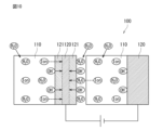
- FIG. 10 is a schematic diagram for explaining anodic oxidation in a film capacitor.
- water (H 2 O), ionic impurities (Ion), etc. contained in the dielectric film 110 react with the electrode film 120 formed of aluminum or the like, causing oxidation on the surface. This is a phenomenon in which a film 121 is formed.
- anodic oxidation occurs, there is a problem that the effective electrode area of the electrode film 120 formed on the dielectric film 110 decreases, resulting in a decrease in capacitance or an increase in ESR of the film capacitor.
- Providing voids between dielectric films 110 has been considered in order to reduce anodic oxidation.
- the present inventors discovered that if the gap between the dielectric films is too large, the capacitance of the film capacitor becomes smaller than the designed value, so it is difficult to appropriately control the size of the gap. found it to be important.
- the voids are formed by expanding gas such as air remaining in the film, so it is difficult to control the size of the voids. Therefore, there is a problem that the gap becomes larger than desired, and the capacitance of the film capacitor decreases.
- the present inventors studied the appropriate thickness of the void and studied a film capacitor that can suppress the decrease in capacitance while reducing the degree of anodic oxidation, and arrived at the following invention.
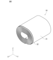
- FIG. 1 is a perspective view showing a film capacitor according to Embodiment 1 of the present invention. Note that the X, Y, and Z directions in the figure indicate the horizontal direction, vertical direction, and height direction of the film capacitor 1, respectively.
- the film capacitor 1 includes a pair of dielectric film windings 10 and a pair of end surface electrodes 20 formed at both ends of the windings 10.
- the rolled body 10 is formed by stacking a pair of dielectric films each having a metal vapor-deposited electrode formed on the surface in the thickness direction, then winding and pressing into a flat shape. Note that the wound body 10 may be formed by laminating and pressing a plurality of dielectric films.
- the wound body 10 has a shape in which the dimension ⁇ 1 in the first direction (Z direction) is shorter than the dimension d1 in the second direction (Y direction) in a cross section along the plane (YZ plane) in which the end electrode 20 extends. have. In other words, the wound body 10 is formed into a columnar shape having an oval cross section.
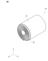
- FIG. 2 is a perspective view showing a wound body without protective winding.
- a protective winding is formed on the surface of the wound body 10 to protect the dielectric film.
- the wound body 10 is formed by winding a pair of dielectric films 31 and 32 overlapping each other in the thickness direction. More specifically, after overlapping one dielectric film 31 and the other dielectric film 32, the pair of dielectric films 31 and 32 are rolled up and pressed into a flat shape, thereby forming an oblong cross section.
- a wound body 10 having the following is formed.
- the dielectric film examples include a plastic film containing a thermoplastic resin such as polyethylene terephthalate, polypropylene, polyphenylene sulfide, or polyethylene naphthalate, or a hydroxyl group (OH group) possessed by the first organic material and an isocyanate possessed by the second organic material.
- a plastic film containing a thermosetting resin such as a cured product obtained by reacting with a group (NCO group) can be used.
- metal such as aluminum or zinc can be used as the metal vapor-deposited electrode formed on the surface of the dielectric film.
- the end electrodes 20 can be formed by spraying metal such as zinc on both ends of the wound body 10, for example.
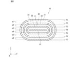
- FIG. 3 is a diagram schematically showing a cross section of the wound body of FIG. 2.
- a gap 41 is provided between the pair of dielectric films 31 and 32.
- the void portion 41 can be formed by overlapping and winding a pair of dielectric films 31 so as to include an air layer between the dielectric films 31 and 32.
- the ratio of the thickness of the void in the height direction of the wound body 10 to the thickness of the dielectric films 31 and 32 is 0.003 or more and 0.029 or less.
- the thickness of the dielectric films 31 and 32 indicates the total thickness f1 to f7 of the dielectric films 31 and 32 laminated in the first direction (Z direction) of the wound body 10. Further, the thickness of the void portion 41 in the height direction (Z direction) of the wound body 10 indicates the sum of the thicknesses s1 to s6 of the void portion 41 in the first direction.
- the ratio of the thickness of the gap to the thickness of the dielectric films 31 and 32 is the sum of the thicknesses s1 to s6 of the gap 41 to the sum of the thicknesses f1 to f7 of the dielectric films 31 and 32. Show ratio.
- the size of the void 41 is such that the sum of the thicknesses s1 to s6 of the void 41 is 0.003 or more and 0.029 or less relative to the sum of the thicknesses f1 to f7 of the dielectric films 31 and 32. is set.
- the void portion 41 does not necessarily have to be formed to have a uniform thickness, and there may be a portion where the dielectric films 31 and 32 are in contact.
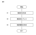
- FIG. 4 is a flowchart showing a method for manufacturing a film capacitor according to Embodiment 1 of the present invention.
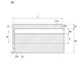
- FIG. 5 is a schematic diagram showing a pair of dielectric films of the film capacitor of FIG. 1.
- FIG. 6 is a schematic perspective view showing a state in which the dielectric film of FIG. 5 is wound.
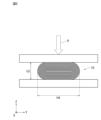
- FIG. 7 is a schematic cross-sectional view showing the process of pressing the rolled body of dielectric film shown in FIG. 6.
- FIG. 8 is a schematic cross-sectional view showing the process of pressing the rolled body of dielectric film shown in FIG. 6.
- a method for manufacturing the film capacitor 1 will be described with reference to FIGS. 4 to 8.
- step S1 the rolled body 10 is formed.
- a pair of dielectric films 31 and 32 on which metal is vapor-deposited are stacked in the thickness direction.
- the dielectric films 31 and 32 are strip-shaped dielectric films having a length L, and metal vapor-deposited electrodes 31a and 32a are formed on the surface of the dielectric films.
- the metal vapor deposited electrodes 31a, 32a are formed on the surfaces of the dielectric films 31, 32 except for the insulation margins 31b, 32b.
- a pattern margin (not shown) in which metal is not vapor-deposited may be formed in the metal-deposited electrodes 31a and 32a.
- the pair of dielectric films 31 and 32 are stacked on top of each other while being shifted by a length As in the width direction W.
- overlapping the dielectric films 31 and 32 in this way it is possible to suppress the occurrence of a short circuit between the metal vapor deposited electrodes 31a and 32a and the end surface electrode 20 after the end surface electrode 20 is formed in a later step. can.
- the stacked pair of dielectric films 31 and 32 are wound to form a cylindrical wound body 10, as shown in FIG.
- h2 are substantially the same, and the wound body 10 has a cylindrical shape with a substantially circular cross section.
- step S2 the rolled body 10 is pressed.
- the side surface of the cylindrical rolled body 10 is pressed to form a flat rolled body 10.
- the flat rolled body 10 can be formed by placing the cylindrical rolled body 10 in a press device and applying pressure in the direction of arrow P.
- the pressing pressure By adjusting the pressing pressure, the thickness of the gap 41 between the dielectric films 31 and 32 can be adjusted. More specifically, as the press pressure increases, the thickness of the void 41 becomes smaller.
- the wound body 10 in step S2 as shown in FIG. becomes smaller.
- step S3 end electrodes 20 are formed on the pressed wound body, and the film capacitor 1 shown in FIG. 1 is completed.
- the end electrodes 20 can be formed by spraying a metal such as zinc on both ends of the wound body 10, for example.
- ⁇ Film capacitor> a film capacitor is used in which the ratio of the thickness of the cavity 41 to the thickness of the dielectric films 31 and 32 is changed from 0 to 0.06 by changing the press pressure in 11 steps. The deviation from the design capacity value and the degree of anodic oxidation were measured.
- ⁇ Thickness of void> The ratio of the thickness of the gap to the thickness of the dielectric film of each film capacitor was calculated by the following method.
- the height ⁇ 1 (see FIG. 1) of the film capacitor in the first direction is measured.
- the film capacitor is disassembled and the number of turns of the dielectric film is determined.
- the obtained number of turns is T film and the thickness of the dielectric film is d film .
- the thickness of the dielectric film also includes the thickness of the metal vapor-deposited electrode.
- the number of turns of the first winding and protective winding other than the dielectric film in the film capacitor is determined in the same manner.
- the first winding is the part that becomes the core when winding the dielectric film
- the protective winding is the part that is wound around the outer periphery to protect the dielectric film and the metal-deposited electrode.
- the number of turns of the first winding is T in , the film thickness is d in , the number of turns of the protective winding is T out , and the film thickness is d out .
- the height ⁇ 0 of the film capacitor in the first direction, assuming that no void is formed, is calculated using equation (1).
- the thickness in the first direction was calculated by "number of windings x film thickness x 2". Since two dielectric films are wound as a pair, one winding includes four layers in the first direction, so the thickness in the first direction was calculated as "number of turns x film thickness x 4". .
- the thickness D of the void included in the film capacitor can be calculated.
- the thickness d air of the air gap per sheet of the dielectric film is calculated using equation (3).
- the ratio R of the thickness of the gap to the thickness of the dielectric film is calculated using equation (4).
- the design capacitance value of the film capacitor can be calculated as follows.
- the film width A0 of the dielectric film, the effective electrode width A, the insulation margin width Am, and the length L of the dielectric film are measured (see FIG. 5).
- the effective electrode width A indicates the width of the metal-deposited electrode that actually acts as a capacitor.
- ⁇ 0 be the dielectric constant of vacuum
- ⁇ film be the relative dielectric constant of the dielectric film
- N be the effective electrode area ratio.
- the effective electrode area ratio N indicates the ratio of the area of the effective electrode calculated from "effective electrode width A x length L of dielectric film” excluding pattern margin and the like.
- Sp indicates an area on which metal such as a pattern margin is not deposited.
- the design capacitance value C0 of the film capacitor can be calculated using equation (5).
- the capacitance loss ⁇ C with respect to the designed capacitance value C0 of each film capacitor can be calculated by equation (6) using the measured capacitance value C1 and the designed capacitance value C0 of each film capacitor.
- the film capacitor was disassembled and the percentage of the area that was discolored white due to anodic oxidation among the effective electrode area was calculated. Note that the portions that were discolored white due to anodic oxidation were visually determined. Note that the difference between discolored areas and non-discolored areas is clear by visual observation, and there is no substantial difference in the area ratio results compared to when image processing technology is used.
- the effective electrode area A all was calculated from "length L of dielectric film x effective electrode width A". Assuming that the area of the white portion due to anodic oxidation is A ox , the degree of anodic oxidation O can be calculated using equation (7).
- FIG. 9 is a table showing the measurement results of capacity loss and degree of anodic oxidation. With reference to FIG. 9, a preferable range of the thickness of the cavity 41 will be discussed.
- the capacitance loss ⁇ C which indicates how much the measured capacitance value C1 of the film capacitor has decreased with respect to the designed capacitance value C0, is It is within 10%. This is because the capacitance loss ⁇ C increases as the thickness of the gap between the dielectric films increases.
- the product standard for film capacitors requires that the capacitance loss ⁇ C with respect to the design capacitance value C0 be within 10%, so it is desirable that the ratio R of the thickness of the void is 0.029 or less.
- the ratio R of the thickness of the void to the thickness of the dielectric film is 0.003 or more, the degree of anodic oxidation can be suppressed to within 5%.
- the degree of anodization increases, the equivalent series resistance (ESR) when a voltage is applied to the film capacitor increases.
- ESR equivalent series resistance
- Product standards for film capacitors require that the increase rate of ESR be within 50%, and by keeping the degree of anodic oxidation within 5%, the product standards can be more reliably met. For this reason, it is desirable that the ratio R of the thickness of the void portion is 0.003 or more.
- the rate of increase in ESR is an index indicating how much ESR increases before and after a high temperature and high humidity test, for example.
- the ratio R of the thickness of the void to the thickness of the dielectric film is preferably 0.003 or more and 0.029 or less.
- the film capacitor 1 includes a wound body 10 and a pair of end surface electrodes 20.
- the wound body 10 is formed by winding a pair of dielectric films 31 and 32 on which metal is vapor-deposited and overlapped in the thickness direction. End surface electrodes 20 are formed at both ends of the wound body 10.
- a gap 41 is formed between the pair of dielectric films 31 and 32.
- the wound body 10 has a dimension ⁇ 1 in the first direction (Z direction) and a dimension in the second direction (Y direction) perpendicular to the first direction in a cross section along the plane (YZ plane) in which the end electrode 20 extends. It has a shorter shape than d1.
- the ratio of the thickness of the void portion 41 in the height direction of the wound body 10 to the thickness of the dielectric films 31 and 32 in the first direction is 0.003 or more and 0.029 or less.
- anodic oxidation of the film capacitor 1 can be suppressed.
- anodic oxidation of the metal vapor deposited electrodes 31a and 32a can be prevented.
- the thickness ratio of the void portion 41 to 0.003 or more and 0.029 or less, the capacitance loss of the film capacitor 1 can be suppressed. Therefore, it is possible to provide a film capacitor 1 in which anodic oxidation is unlikely to occur and the capacitance loss is small.
- the method for manufacturing the film capacitor 1 includes the steps of forming a wound body, pressing the wound body, and forming end surface electrodes.
- the step of forming the wound body includes winding a pair of dielectric films 31 and 32 on which metal is vapor-deposited, overlapping each other in the thickness direction.
- the step of pressing the wound body includes controlling the thickness of the gap 41 formed between the pair of dielectric films 31 and 32 by controlling the pressing pressure within a predetermined range.
- the film capacitor of the present invention includes a pair of wound bodies of dielectric films on which metal is vapor-deposited and overlapped in the thickness direction, and a pair of end face electrodes formed at both ends of the wound body. , a gap is formed between the pair of dielectric films, and the wound body has a dimension in the first direction in a second direction perpendicular to the first direction in a cross section along a surface in which the end electrode extends.
- the ratio of the thickness of the gap in the height direction of the wound body to the thickness of the dielectric film in the first direction is 0.003 or more and 0.029 or less.
- the method for manufacturing a film capacitor of the present invention includes the steps of stacking and winding a pair of dielectric films on which metal is vapor-deposited in the thickness direction to form a wound body, and pressing the wound body. and a step of forming end face electrodes at both ends of the wound body, and the step of pressing the wound body includes forming end electrodes between the pair of dielectric films by controlling the pressing pressure within a predetermined range.
- the thickness of the void portion is controlled to be 0.003 or more and 0.029 or less relative to the thickness of the dielectric film.
- the present invention is useful for film capacitors used in various electronic devices, electrical devices, industrial devices, vehicle devices, etc.
Landscapes
- Engineering & Computer Science (AREA)
- Power Engineering (AREA)
- Manufacturing & Machinery (AREA)
- Microelectronics & Electronic Packaging (AREA)
- Fixed Capacitors And Capacitor Manufacturing Machines (AREA)
Abstract
Description
表面に金属が蒸着され、厚み方向に重なった一対の誘電体フィルムの巻回体と、
前記巻回体の両端に形成された一対の端面電極と、
を備え、
前記一対の前記誘電体フィルムの間には空隙部が形成され、
前記巻回体は、前記端面電極の延びる面に沿った方向の断面において、第1方向の寸法が前記第1方向に直交する第2方向の寸法よりも短い形状を有し、前記第1方向における前記誘電体フィルムの厚さに対する前記空隙部の厚さの比率は、0.003以上0.029以下である。
表面に金属が蒸着された一対の誘電体フィルムを厚み方向に重ねて巻回して巻回体を形成するステップと、
前記巻回体をプレスするステップと、
前記巻回体の両端部に端面電極を形成するステップと、
を含み、
前記巻回体をプレスするステップは、プレス圧力を所定範囲に制御することにより、前記一対の誘電体フィルムの間に形成される空隙の厚さを、前記誘電体フィルムの厚さに対して0.003以上0.029以下に制御する。
特許文献1に記載のフィルムコンデンサでは、巻回体の巻回軸に垂直な断面において、有効部の直径を、メタリコン電極の直径よりも大きくして、メタリコン電極の体積比率を低減して、フィルムコンデンサの小型化、高容量化を図ることが提案されている。特許文献1のフィルムコンデンサでは、誘電体フィルムと第1電極膜および第2電極膜とを巻回した本体に残存している空気などの気体を膨張させることにより、誘電体フィルムの間に空隙を形成して、有効部の直径を大きくしている。
[全体構成]
図1は、本発明の実施の形態1にかかるフィルムコンデンサを示す斜視図である。なお、図中のX、Y、Z方向はそれぞれ、フィルムコンデンサ1の横方向、縦方向、高さ方向を示す。
図4は、本発明の実施の形態1にかかるフィルムコンデンサの製造方法を示すフローチャートである。図5は、図1のフィルムコンデンサの一対の誘電体フィルムを示す模式図である。図6は、図5の誘電体フィルムを巻回した状態を示す概略斜視図である。図7は、図6の誘電体フィルムの巻回体をプレスする工程を示す概略断面図である。図8は、図6の誘電体フィルムの巻回体をプレスする工程を示す概略断面図である。図4~図8を参照して、フィルムコンデンサ1の製造方法について説明する。
実施の形態1で説明したフィルムコンデンサにおいて、巻回体10をプレスする工程(図4のステップS2)におけるプレス圧力を変化させることで、空隙部41の厚さを変化させて、フィルムコンデンサ1の設計容量値に対するずれおよび陽極酸化度を測定した。具体的な結果は図9の通りである。
実施例では、プレス圧力を11段階に変化させることにより、誘電体フィルム31、32の厚さに対する空隙部41の厚さの比率を0から0.06まで変化させたフィルムコンデンサを使用して、設計容量値に対するずれおよび陽極酸化度を測定した。
それぞれのフィルムコンデンサの誘電体フィルムの厚さに対する空隙部の厚さの比率は、以下の方法で算出した。
フィルムコンデンサの設計容量値は、以下の通り算出することができる。
それぞれのフィルムコンデンサの設計容量値C0に対する容量損失ΔCは、それぞれのフィルムコンデンサの実測容量値C1と設計容量値C0を用いて、式(6)により算出することができる。
それぞれのプレス圧力で空隙部41の厚さを調整したフィルムコンデンサに対して、高温高湿試験を実施し、高温高湿試験後の陽極酸化度を測定した。陽極酸化度は、誘電体フィルム31、32の金属蒸着電極31a、32aが白色に変色している面積の割合を求めることにより測定した。
図9は、容量損失および陽極酸化度の測定結果を示す表である。図9を参照して、空隙部41の厚さの好ましい範囲について検討する。
上述した実施の形態によると、以下の効果を奏することができる。
(1)本発明のフィルムコンデンサは、表面に金属が蒸着され、厚み方向に重なった一対の誘電体フィルムの巻回体と、巻回体の両端に形成された一対の端面電極と、を備え、一対の前記誘電体フィルムの間には空隙部が形成され、巻回体は、端面電極の延びる面に沿った方向の断面において、第1方向の寸法が第1方向に直交する第2方向の寸法よりも短い形状を有し、第1方向における誘電体フィルムの厚さに対する巻回体の高さ方向の空隙部の厚さの比率は、0.003以上0.029以下である。
10 巻回体
20 端面電極
31、32 誘電体フィルム
31a、32a 金属蒸着電極
31b、32b 絶縁マージン
41 空隙部
Claims (3)
- 表面に金属が蒸着され、厚み方向に重なった一対の誘電体フィルムの巻回体と、
前記巻回体の両端に形成された一対の端面電極と、
を備え、
前記一対の前記誘電体フィルムの間には空隙部が形成され、
前記巻回体は、前記端面電極の延びる面に沿った方向の断面において、第1方向の寸法が前記第1方向に直交する第2方向の寸法よりも短い形状を有し、前記第1方向における前記誘電体フィルムの厚さに対する前記空隙部の厚さの比率は、0.003以上0.029以下である、
フィルムコンデンサ。 - 前記フィルムコンデンサの設計容量値をC0、実測容量値をC1としたときに、(C0-C1)/C0×100が10%以下である、
請求項1に記載のフィルムコンデンサ。 - 表面に金属が蒸着された一対の誘電体フィルムを厚み方向に重ねて巻回して巻回体を形成するステップと、
前記巻回体をプレスするステップと、
前記巻回体の両端部に端面電極を形成するステップと、
を含み、
前記巻回体をプレスするステップは、プレス圧力を所定範囲に制御することにより、前記一対の誘電体フィルムの間に形成される空隙部の厚さを、前記誘電体フィルムの厚さに対して0.003以上0.029以下に制御する、
フィルムコンデンサの製造方法。
Priority Applications (3)
| Application Number | Priority Date | Filing Date | Title |
|---|---|---|---|
| JP2024531948A JP7840408B2 (ja) | 2022-07-07 | 2023-05-26 | フィルムコンデンサおよびフィルムコンデンサの製造方法 |
| CN202380051019.6A CN119452442A (zh) | 2022-07-07 | 2023-05-26 | 薄膜电容器以及薄膜电容器的制造方法 |
| US19/005,100 US20250149251A1 (en) | 2022-07-07 | 2024-12-30 | Film capacitor and method for producing film capacitor |
Applications Claiming Priority (2)
| Application Number | Priority Date | Filing Date | Title |
|---|---|---|---|
| JP2022109950 | 2022-07-07 | ||
| JP2022-109950 | 2022-07-07 |
Related Child Applications (1)
| Application Number | Title | Priority Date | Filing Date |
|---|---|---|---|
| US19/005,100 Continuation US20250149251A1 (en) | 2022-07-07 | 2024-12-30 | Film capacitor and method for producing film capacitor |
Publications (1)
| Publication Number | Publication Date |
|---|---|
| WO2024009644A1 true WO2024009644A1 (ja) | 2024-01-11 |
Family
ID=89453070
Family Applications (1)
| Application Number | Title | Priority Date | Filing Date |
|---|---|---|---|
| PCT/JP2023/019730 Ceased WO2024009644A1 (ja) | 2022-07-07 | 2023-05-26 | フィルムコンデンサおよびフィルムコンデンサの製造方法 |
Country Status (4)
| Country | Link |
|---|---|
| US (1) | US20250149251A1 (ja) |
| JP (1) | JP7840408B2 (ja) |
| CN (1) | CN119452442A (ja) |
| WO (1) | WO2024009644A1 (ja) |
Citations (3)
| Publication number | Priority date | Publication date | Assignee | Title |
|---|---|---|---|---|
| JPH04291711A (ja) * | 1991-03-20 | 1992-10-15 | Matsushita Electric Ind Co Ltd | コンデンサ |
| JPH1167580A (ja) * | 1997-08-21 | 1999-03-09 | Oji Paper Co Ltd | 金属化フィルムコンデンサの製造方法 |
| JP2015103700A (ja) * | 2013-11-26 | 2015-06-04 | 京セラ株式会社 | フィルムコンデンサ |
-
2023
- 2023-05-26 JP JP2024531948A patent/JP7840408B2/ja active Active
- 2023-05-26 WO PCT/JP2023/019730 patent/WO2024009644A1/ja not_active Ceased
- 2023-05-26 CN CN202380051019.6A patent/CN119452442A/zh active Pending
-
2024
- 2024-12-30 US US19/005,100 patent/US20250149251A1/en active Pending
Patent Citations (3)
| Publication number | Priority date | Publication date | Assignee | Title |
|---|---|---|---|---|
| JPH04291711A (ja) * | 1991-03-20 | 1992-10-15 | Matsushita Electric Ind Co Ltd | コンデンサ |
| JPH1167580A (ja) * | 1997-08-21 | 1999-03-09 | Oji Paper Co Ltd | 金属化フィルムコンデンサの製造方法 |
| JP2015103700A (ja) * | 2013-11-26 | 2015-06-04 | 京セラ株式会社 | フィルムコンデンサ |
Also Published As
| Publication number | Publication date |
|---|---|
| JPWO2024009644A1 (ja) | 2024-01-11 |
| US20250149251A1 (en) | 2025-05-08 |
| CN119452442A (zh) | 2025-02-14 |
| JP7840408B2 (ja) | 2026-04-03 |
Similar Documents
| Publication | Publication Date | Title |
|---|---|---|
| JPS59105311A (ja) | 長円形2重コンデンサ−パツケ−ジ | |
| US7663864B2 (en) | Electrolytic capacitor | |
| JPH0793236B2 (ja) | フイルムコンデンサおよびその製造方法 | |
| KR20090086146A (ko) | 전해 콘덴서와 그 제조 방법 | |
| CA2627041A1 (en) | A capacitor element, a method for manufacturing a capacitor element, and the use of a power capacitor | |
| EP3016120A1 (en) | Film capacitor | |
| JP7840408B2 (ja) | フィルムコンデンサおよびフィルムコンデンサの製造方法 | |
| EP2715751A1 (en) | Polytetrafluoroethylene film capacitor | |
| US8529641B2 (en) | Electrolytic capacitor and method of manufacturing the same | |
| JP6430328B2 (ja) | コンデンサ素子の製造方法 | |
| JP2021174789A (ja) | 電解コンデンサ用セパレータの製造方法および電解コンデンサ | |
| JPH08102427A (ja) | フィルムコンデンサ | |
| JP2005093761A (ja) | フィルムコンデンサ | |
| US12525407B2 (en) | Electrode foil for electrolytic capacitors, and electrolytic capacitor | |
| JP2008091958A (ja) | 偏平形金属化フィルムコンデンサの製造方法 | |
| JP2009277866A (ja) | フィルムコンデンサ及びその製造方法 | |
| CN113436885A (zh) | 云母纸电容器及其制备方法 | |
| JPS58153322A (ja) | コンデンサ | |
| JP7670733B2 (ja) | フィルムコンデンサ | |
| JP2010040573A (ja) | フィルムコンデンサ及びその製造方法 | |
| JP2572616Y2 (ja) | 金属化フィルムコンデンサ | |
| JP2008098675A (ja) | 偏平形金属化フィルムコンデンサ | |
| JPH05109583A (ja) | フイルムコンデンサ | |
| JP2016046291A (ja) | フィルムコンデンサ素子及びその製造方法 | |
| US20250149256A1 (en) | Metal foil for producing electrode foil, method for producing electrode foil for electrolytic capacitor use, electrode foil for electrolytic capacitor use, and electrolytic capacitor |
Legal Events
| Date | Code | Title | Description |
|---|---|---|---|
| 121 | Ep: the epo has been informed by wipo that ep was designated in this application |
Ref document number: 23835180 Country of ref document: EP Kind code of ref document: A1 |
|
| WWE | Wipo information: entry into national phase |
Ref document number: 2024531948 Country of ref document: JP |
|
| WWE | Wipo information: entry into national phase |
Ref document number: 202380051019.6 Country of ref document: CN |
|
| NENP | Non-entry into the national phase |
Ref country code: DE |
|
| WWP | Wipo information: published in national office |
Ref document number: 202380051019.6 Country of ref document: CN |
|
| 122 | Ep: pct application non-entry in european phase |
Ref document number: 23835180 Country of ref document: EP Kind code of ref document: A1 |