WO2024009343A1 - 光検出装置 - Google Patents
光検出装置 Download PDFInfo
- Publication number
- WO2024009343A1 WO2024009343A1 PCT/JP2022/026565 JP2022026565W WO2024009343A1 WO 2024009343 A1 WO2024009343 A1 WO 2024009343A1 JP 2022026565 W JP2022026565 W JP 2022026565W WO 2024009343 A1 WO2024009343 A1 WO 2024009343A1
- Authority
- WO
- WIPO (PCT)
- Prior art keywords
- period
- selects
- pixels
- pulse signal
- signal
- Prior art date
- Legal status (The legal status is an assumption and is not a legal conclusion. Google has not performed a legal analysis and makes no representation as to the accuracy of the status listed.)
- Ceased
Links
Images



















Classifications
-
- H—ELECTRICITY
- H04—ELECTRIC COMMUNICATION TECHNIQUE
- H04N—PICTORIAL COMMUNICATION, e.g. TELEVISION
- H04N23/00—Cameras or camera modules comprising electronic image sensors; Control thereof
- H04N23/50—Constructional details
- H04N23/55—Optical parts specially adapted for electronic image sensors; Mounting thereof
-
- G—PHYSICS
- G01—MEASURING; TESTING
- G01J—MEASUREMENT OF INTENSITY, VELOCITY, SPECTRAL CONTENT, POLARISATION, PHASE OR PULSE CHARACTERISTICS OF INFRARED, VISIBLE OR ULTRAVIOLET LIGHT; COLORIMETRY; RADIATION PYROMETRY
- G01J1/00—Photometry, e.g. photographic exposure meter
- G01J1/42—Photometry, e.g. photographic exposure meter using electric radiation detectors
-
- G—PHYSICS
- G01—MEASURING; TESTING
- G01J—MEASUREMENT OF INTENSITY, VELOCITY, SPECTRAL CONTENT, POLARISATION, PHASE OR PULSE CHARACTERISTICS OF INFRARED, VISIBLE OR ULTRAVIOLET LIGHT; COLORIMETRY; RADIATION PYROMETRY
- G01J11/00—Measuring the characteristics of individual optical pulses or of optical pulse trains
-
- H—ELECTRICITY
- H04—ELECTRIC COMMUNICATION TECHNIQUE
- H04N—PICTORIAL COMMUNICATION, e.g. TELEVISION
- H04N23/00—Cameras or camera modules comprising electronic image sensors; Control thereof
- H04N23/60—Control of cameras or camera modules
- H04N23/665—Control of cameras or camera modules involving internal camera communication with the image sensor, e.g. synchronising or multiplexing SSIS control signals
-
- H—ELECTRICITY
- H04—ELECTRIC COMMUNICATION TECHNIQUE
- H04N—PICTORIAL COMMUNICATION, e.g. TELEVISION
- H04N25/00—Circuitry of solid-state image sensors [SSIS]; Control thereof
- H04N25/50—Control of the SSIS exposure
- H04N25/53—Control of the integration time
-
- H—ELECTRICITY
- H04—ELECTRIC COMMUNICATION TECHNIQUE
- H04N—PICTORIAL COMMUNICATION, e.g. TELEVISION
- H04N25/00—Circuitry of solid-state image sensors [SSIS]; Control thereof
- H04N25/70—SSIS architectures; Circuits associated therewith
- H04N25/76—Addressed sensors, e.g. MOS or CMOS sensors
- H04N25/77—Pixel circuitry, e.g. memories, A/D converters, pixel amplifiers, shared circuits or shared components
-
- H—ELECTRICITY
- H04—ELECTRIC COMMUNICATION TECHNIQUE
- H04N—PICTORIAL COMMUNICATION, e.g. TELEVISION
- H04N25/00—Circuitry of solid-state image sensors [SSIS]; Control thereof
- H04N25/70—SSIS architectures; Circuits associated therewith
- H04N25/76—Addressed sensors, e.g. MOS or CMOS sensors
- H04N25/77—Pixel circuitry, e.g. memories, A/D converters, pixel amplifiers, shared circuits or shared components
- H04N25/772—Pixel circuitry, e.g. memories, A/D converters, pixel amplifiers, shared circuits or shared components comprising A/D, V/T, V/F, I/T or I/F converters
- H04N25/773—Pixel circuitry, e.g. memories, A/D converters, pixel amplifiers, shared circuits or shared components comprising A/D, V/T, V/F, I/T or I/F converters comprising photon counting circuits, e.g. single photon detection [SPD] or single photon avalanche diodes [SPAD]
Definitions
- the present technology relates to a photodetection device. Specifically, the present invention relates to a photodetection device that counts the number of photons.
- solid-state image sensors in which a plurality of pixels are arranged are used in imaging devices and the like to capture image data.
- a photodetection device has been proposed in which each pixel is provided with a SPAD (Single-Photon Avalanche Diode), a waveform shaping section that generates a pulse signal, and a counter that counts the number of pulses (see, for example, Patent Document 1). ).
- SPAD Single-Photon Avalanche Diode
- a waveform shaping section that generates a pulse signal
- a counter that counts the number of pulses
- the linearity of the composite signal is ensured by adding pixels when one of the two pixel counters is saturated.
- the maximum count value of each pixel cannot be increased, and the dynamic range cannot be expanded. If the resolution of each counter of each pixel is increased, the dynamic range can be expanded and the image quality can be improved, but this is not preferable because the circuit scale of the counter increases.
- This technology was created in view of this situation, and its purpose is to improve the image quality in a photodetection device that counts the number of pulses with a counter.
- the present technology has been developed to solve the above-mentioned problems, and its first aspect includes a first sensor section that generates a first pulse signal in response to incident photons; a second sensor unit that generates a second pulse signal in response to a second pulse signal; and a second sensor unit that counts a count value in synchronization with any of a plurality of signals including the first and second pulse signals, and indicates the count value.
- a first counter that outputs a first digital signal and a first carry flag indicating whether an overflow has occurred;
- the photodetector includes a second counter that counts a count value and outputs a second digital signal indicating the count value. This has the effect of expanding the resolution of the counter.
- a first multiplexer that selects one of the first and second pulse signals and outputs the selected one to the first counter as a first output signal; further comprising a second multiplexer that selects either the flag or the second pulse signal and outputs it to the second counter as a second output signal, the first counter
- the second counter may count in synchronization with the second output signal. This brings about the effect that the number of pulses is counted in synchronization with the output signal of the multiplexer.
- the first multiplexer selects the first pulse signal when a low illuminance mode is set in which the illuminance does not exceed the predetermined value, and selects the first pulse signal when the illuminance is higher than the predetermined value.
- the second multiplexer alternately selects the first and second pulse signals when the high-light mode is set, and selects the second pulse signal when the low-light mode is set. If the high-intensity mode is selected and the high-intensity mode is set, the first carry flag may be selected. This brings about the effect that the resolution of the counter is expanded at times of high illuminance.
- the illuminance is higher than the predetermined value based on the first and second digital signals, and either the high illuminance mode or the low illuminance mode is set. It may further include a determiner. This brings about the effect that the illuminance is determined within the pixel.
- At least one of the first and second counters outputs a specific bit of the digital signal to the determiner, and the determiner outputs the specific bit based on the specific bit.
- Either the high illumination mode or the low illumination mode may be set. This has the effect of simplifying the determiner.
- the first sensor section is disposed on one of the first and second pixels of the same color among the plurality of pixels arranged in the pixel array section, and the second sensor section is disposed on the other side. may be arranged. This brings about the effect of suppressing the difference in count values for each pixel.
- a microlens may be further provided that guides the incident light to a plurality of pixels of the same color including the first and second pixels. This brings about the effect that the phase difference can be easily detected.
- the first and second sensor sections further include a control circuit that controls the first and second sensor sections, and each of the first and second sensor sections includes an avalanche photodiode and an avalanche photodiode.
- a recharge transistor that performs recharging to return the cathode potential of the battery to a predetermined potential; the control circuit controls a count period, which is an interval at which the recharge is performed, to one of a plurality of cycles; If the count period is a long period longer than the predetermined period, the first pulse signal is selected, and if the count period is a short period shorter than the predetermined period, the first and second pulse signals are selected.
- the second multiplexer selects the second pulse signal when the count period is the long period, and selects the first pulse signal when the count period is the short period.
- a carry flag may be selected. This brings about the effect of reducing power consumption.
- the first and second counters may determine whether or not the counting period of the first and second counters is enabled within one of the long period and the short period.
- the first and second sensor sections each include a logic gate that turns off the recharge transistor when it is determined that counting is invalidated. It may further include. This brings about the effect that counting is controlled to be valid or invalid depending on the illuminance.
- the first sensor section is arranged in one of the first and second pixels among the plurality of pixels arranged in the pixel array section, and the second sensor section is arranged in the other one.
- the control circuit switches the count period a plurality of times within a frame period for capturing one frame, and the first and second multiplexers switch the selected count period within the frame period. The switching may be performed multiple times. This brings about the effect of reducing power consumption.
- control circuit may sequentially select a plurality of rows of the pixel array section and start exposure. This brings about the effect of improving the frame rate.
- control circuit selects all pixels in the pixel array section at the start of the frame period to simultaneously start exposure, and selects all the pixels immediately before the end of the frame period. Exposure may be terminated at the same time. This brings about the effect of suppressing rolling shutter distortion.
- control circuit may sequentially select a plurality of rows of the pixel array section and start exposure during the frame period. This brings about the effect of improving the frame rate.
- control circuit selects all the pixels during the frame period and ends the exposure at the same time, switches the count period after completing reading of all the pixels, and then selects all the pixels. You may select them and start exposure at the same time. This brings about the effect of suppressing rolling shutter distortion.
- control circuit simultaneously selects and exposes one of the first and second rows that share a signal line that transmits the digital signal, and during reading of the one digital signal, The other of the first and second rows may be selected and exposed at the same time. This brings about the effect of improving the frame rate.
- a first logic gate that outputs a result of a logical operation on the first and second pulse signals as a first operation result; a first multiplexer that selects one of a plurality of signals including the calculation result and outputs it to the first counter as a first output signal; a second multiplexer that selects one and outputs it to the second counter as a second output signal; the first counter counts in synchronization with the first output signal; The second counter may count in synchronization with the second output signal.
- the first and second sensor sections further include a control circuit that controls the first and second sensor sections, and each of the first and second sensor sections includes an avalanche photodiode and an avalanche photodiode.
- a recharge transistor that performs recharging to return the cathode potential of the battery to a predetermined potential; the control circuit controls a count period, which is an interval at which the recharge is performed, to one of a plurality of cycles; If the count period is a long period longer than the predetermined period, the first pulse signal is selected, and if the count period is a short period shorter than the predetermined period, the first and second pulse signals are selected.
- the second multiplexer selects the second pulse signal when the count period is the long period, and selects the first pulse signal when the count period is the short period.
- a carry flag may be selected. This brings about the effect of reducing power consumption.
- a third sensor section that generates a third pulse signal in response to incident photons
- a fourth sensor section that generates a fourth pulse signal in response to incident photons.
- a second logic gate that outputs the result of the logic operation on the third and fourth pulse signals as a second operation result
- a second logic gate that outputs the result of the logic operation on the respective outputs of the first and second logic gates.
- a third logic gate that outputs a third operation result, a second carry flag indicating whether an overflow has occurred, and a third logic gate that outputs either the third pulse signal or the second operation result.
- a third multiplexer that outputs an output signal; a third digital signal that counts a count value in synchronization with the third output signal; a third digital signal that indicates the count value; and a third carry signal that indicates whether an overflow has occurred.
- a third counter that outputs a flag; a fourth multiplexer that outputs either the third carry flag or the fourth pulse signal as a fourth output signal;
- the first multiplexer further includes a fourth counter that synchronously counts a count value and outputs a fourth digital signal indicating the count value, and the first multiplexer is configured to synchronize the first pulse signal with the first pulse signal. Either the calculation result or the third calculation result may be selected, and the second counter may further generate the second carry flag. This brings about the effect that addition of 4 pixels or 2 pixels becomes possible.
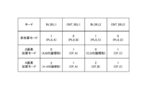
- the first multiplexer selects the first pulse signal when the non-additive low illuminance mode in which the illuminance does not exceed the predetermined value is set; When a higher non-additive high-intensity mode is set, the first pulse signal and the first calculation result are alternately selected, and when the addition mode is set, the first calculation result is selected.
- the second multiplexer selects the second pulse signal when the non-additive low-light mode is set, and selects the first carry signal when the non-additive high-light mode is set. If a flag is selected and the addition mode is set, the first carry flag may be selected. This brings about the effect that the resolution of the counter is expanded during high illuminance or during pixel addition.
- a part of the first sensor part and a part of the second sensor part are arranged on a predetermined pixel chip, and the rest of the first sensor part and the part of the second sensor part are arranged on a predetermined pixel chip.
- the remaining two sensor units and the first and second counters may be arranged on a predetermined circuit chip. This brings about the effect that it becomes easy to increase the number of pixels.
- the first sensor section is further provided with a control circuit that controls the plurality of pixels, and the first sensor section is arranged in one of the first and second pixels among the plurality of pixels, and the first sensor section is arranged in the other one of the first and second pixels.
- the second sensor section may be disposed, and the control circuit may control some of the plurality of pixels to generate a pulse signal. This brings about the effect of reducing read time and data amount.
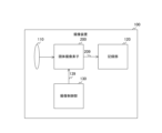
- FIG. 1 is a block diagram illustrating a configuration example of an imaging device according to a first embodiment of the present technology.
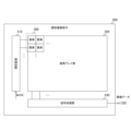
- FIG. 1 is a block diagram showing an example of a configuration of a solid-state image sensor according to a first embodiment of the present technology.
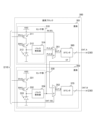
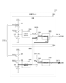
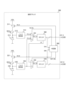
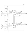
- FIG. 2 is a circuit diagram showing an example of a configuration of a pixel block in the first embodiment of the present technology.
- FIG. 2 is a circuit diagram showing a configuration example of a counter in the first embodiment of the present technology. It is a figure showing an example of operation of a control circuit in a 1st embodiment of this art.
- FIG. 3 is a diagram illustrating an example of a state of a pixel block in a low-light mode in the first embodiment of the present technology.
- FIG. 1 is a block diagram illustrating a configuration example of an imaging device according to a first embodiment of the present technology.
- FIG. 1 is a block diagram showing an example of a configuration of a solid-state image sensor according to a first embodiment of the
- FIG. 3 is a diagram illustrating an example of a state of a pixel block when pixel A is exposed in high-intensity mode in the first embodiment of the present technology.
- FIG. 7 is a diagram illustrating an example of the state of a pixel block when pixel B is exposed in high-intensity mode in the first embodiment of the present technology.
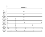
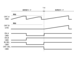
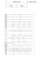
- 5 is a timing chart illustrating an example of the operation of the solid-state image sensor in a low-light mode in the first embodiment of the present technology.
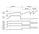
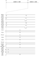
- 5 is a timing chart illustrating an example of the operation of the solid-state image sensor in high-illuminance mode in the first embodiment of the present technology. It is a flow chart which shows an example of operation of a solid-state image sensing device in a 1st embodiment of this art.
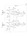
- FIG. 7 is a circuit diagram showing an example of a configuration of a pixel block in a second embodiment of the present technology. It is an example of the timing chart when switching from low illuminance mode to high illuminance mode in the 2nd embodiment of this technology. It is an example of the timing chart when switching from high illuminance mode to low illuminance mode in the 2nd embodiment of this technology.
- FIG. 7 is a circuit diagram showing an example of a configuration of a pixel block in a third embodiment of the present technology. It is an example of the timing chart when switching from low illuminance mode to high illuminance mode in the 3rd embodiment of this technology.
- FIG. 7 is a diagram showing an example of arrangement of pixels within a pixel block in a fourth embodiment of the present technology.
- FIG. 7 is a diagram showing an example of arrangement of pixels in a quad Bayer array according to a fourth embodiment of the present technology.
- FIG. 7 is a diagram illustrating an example of arrangement of pixels within a pixel block in a fifth embodiment of the present technology.
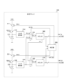
- FIG. 7 is a circuit diagram showing an example of a configuration of a pixel block in a sixth embodiment of the present technology. It is a figure showing an example of operation of a control circuit in a 6th embodiment of this art.
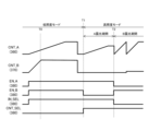
- FIG. 12 is a timing chart showing an example of the operation of the solid-state image sensor during a long period count period in the sixth embodiment of the present technology.
- 13 is a timing chart showing an example of the operation of the solid-state image sensor during the exposure period of pixel A in the short cycle count period in the sixth embodiment of the present technology.
- 12 is a timing chart showing an example of the operation of the solid-state image sensor during the exposure period of pixel B in the short cycle count period in the sixth embodiment of the present technology. It is a figure showing an example of operation of a control circuit in a modification of a 6th embodiment of this art.
- FIG. 7 is a circuit diagram showing an example of a configuration of a pixel block in a seventh embodiment of the present technology.
- FIG. 12 is a timing chart showing an example of the operation of the solid-state image sensor during the exposure period of pixel A in the short cycle count period in the seventh embodiment of the present technology.
- 12 is a timing chart showing an example of the operation of the solid-state image sensor during the exposure period of pixel B in the short cycle count period in the seventh embodiment of the present technology.
- 12 is a timing chart showing an example of the operation of the solid-state image sensor during a long period count period in the seventh embodiment of the present technology.
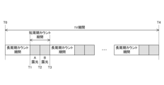
- FIG. 12 is a diagram illustrating an example of a count cycle within a 1V period of a predetermined row in the eighth embodiment of the present technology.
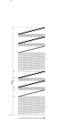
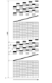
- 12 is a timing chart showing an example of exposure and readout operations of a solid-state image sensor according to a ninth embodiment of the present technology.
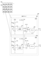
- FIG. 12 is a circuit diagram showing an example of a configuration of a pixel block in a thirteenth embodiment of the present technology. It is a figure showing an example of operation of a control circuit in a 13th embodiment of this technology.
- FIG. 12 is a circuit diagram showing an example of a configuration of a pixel block in a fourteenth embodiment of the present technology. 12 is a timing chart showing an example of the operation of the solid-state image sensor in addition mode in the fourteenth embodiment of the present technology.
- FIG. 12 is a diagram illustrating an example of arrangement of pixels within a pixel block in a fifteenth embodiment of the present technology.
- FIG. 12 is a circuit diagram showing an example of a configuration of a pixel block in a fifteenth embodiment of the present technology. It is a figure showing an example of operation of a control circuit in a 15th embodiment of this technology. It is a figure showing an example of operation of a control circuit in a 16th embodiment of this technology.
- First embodiment (example of expanding the counter during high illuminance) 2.
- Second embodiment (example of determining illuminance and expanding the counter) 3.
- Third embodiment (example of expanding a counter based on specific bits) 4.
- Fourth embodiment (example where two pixels of the same color expand the counter when the illuminance is high) 5.
- Fifth embodiment (example where two pixels under the microlens expand the counter at high illuminance) 6.
- Sixth embodiment (example of expanding the counter when the count cycle is short) 7.
- Seventh embodiment (example of expanding the counter during short cycles and enabling or disabling counting) 8.
- FIG. 1 is a block diagram illustrating a configuration example of an imaging device 100 according to an embodiment of the present technology.
- the imaging device 100 captures image data, and includes an imaging lens 110, a solid-state imaging device 200, a recording section 120, and an imaging control section 130.
- the imaging device 100 for example, a smartphone, a digital camera, a personal computer, or a vehicle-mounted camera is assumed.
- the imaging device 100 is an example of a photodetecting device described in the claims.
- the imaging lens 110 focuses incident light and guides it to the solid-state imaging device 200.
- the solid-state imaging device 200 captures image data under the control of the imaging control unit 130.
- This solid-state image sensor 200 supplies captured image data to the recording unit 120 via a signal line 209.
- the recording unit 120 records image data.
- the imaging control unit 130 controls the solid-state imaging device 200 to capture image data.
- the imaging control unit 130 supplies, for example, a synchronization signal such as a vertical synchronization signal to the solid-state image sensor 200 via a signal line 139.
- the imaging device 100 may further include an interface, and may transmit image data to the outside through the interface, or may further include a display section, and may display image data on the display section.
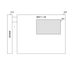
- FIG. 2 is a block diagram showing a configuration example of the solid-state image sensor 200 in the first embodiment of the present technology.
- This solid-state image sensor 200 includes a control circuit 210, a pixel array section 220, and a signal processing section 230. These circuits are placed on a single semiconductor chip.
- a plurality of pixels are arranged in a two-dimensional grid in the pixel array section 220.
- a set of pixels arranged in a predetermined direction horizontal direction, etc.
- a set of pixels arranged in a direction perpendicular to the row will be referred to as a column.
- the pixel array section 220 is divided into a plurality of pixel blocks 300.
- a plurality of pixels are arranged in each pixel block 300.
- two pixels are arranged in the column direction in the pixel block 300.
- each pixel within the pixel block 300 can also be arranged in a row direction or in a diagonal direction.
- the control circuit 210 sequentially selects rows in synchronization with a vertical synchronization signal.
- the pixel counts the number of times photons are incident within the exposure period and outputs a digital signal representing the counted value to the signal processing unit 230 as a pixel signal.
- a mode signal MODE that designates one of a plurality of modes including a high-illuminance mode and a low-illuminance mode is input to the control circuit 210.
- the high-illuminance mode is a mode set during high illuminance when the illuminance is higher than a predetermined value
- the low-illuminance mode is a mode set during low illuminance when the illuminance is below a predetermined value.
- a determination circuit that performs photometry to determine whether the illuminance is higher than a predetermined value and sets the mode is located inside the solid-state image sensor 200 after the pixel array section 220 (such as the signal processing section 230) or the solid-state image sensor. It is arranged outside the element 200.
- the user can also manually set the high-illuminance mode and low-illuminance mode. In this case, the determination circuit becomes unnecessary.
- the signal processing unit 230 performs various signal processing on image data (frame) in which pixel signals are arranged. This signal processing section 230 outputs the processed frame to the recording section 120.
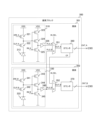
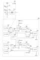
- FIG. 3 is a circuit diagram showing a configuration example of the pixel block 300 in the first embodiment of the present technology. Pixels 301 and 302 are arranged in this pixel block 300.
- the pixel 301 includes a sensor section 310, a multiplexer 351, and a counter 360.
- the pixel 302 includes a sensor section 330, a multiplexer 352, and a counter 370.
- the sensor section 310 includes pMOS transistors 311 and 312, a SPAD 313, and a pulse shaping section 314.
- PMOS transistors 311 and 312 are connected in series between the cathode of SPAD 313 and power supply voltage VDD, with pMOS transistor 311 on the power supply side.
- An enable signal EN_A from the control circuit 210 is input to the gate of the pMOS transistor 311, and a predetermined bias voltage BIAS is applied to the gate of the pMOS transistor 312.
- the pixel 301 When the enable signal EN_A is at a low level, the pixel 301 is enabled, and the cathode potential of the SPAD 313 drops in response to the incidence of photons. On the other hand, when the enable signal EN_A is at a high level, the pixel 301 is disabled, and the cathode potential does not drop even if a photon is incident.
- the pulse shaping unit 314 detects a drop in the cathode potential of the SPAD 313, shapes the waveform, and generates the pulse signal PLS_A. This pulse shaping section 314 supplies the pulse signal PLS_A to the multiplexer 351.
- the sensor section 330 includes pMOS transistors 331 and 332, a SPAD 333, and a pulse shaping section 334, and has the same circuit configuration as the sensor section 310.
- the enable signal EN_B from the control circuit 210 is input to the gate of the pMOS transistor 331, and the pulse shaping section 334 generates a pulse signal PLS_B and supplies it to the multiplexers 351 and 352.
- the multiplexer 351 selects one of the pulse signals PLS_A and PLS_B according to the selection signal IN_SEL from the control circuit 210 and outputs it to the counter 360 as an output signal OUT_A. For example, when the selection signal IN_SEL is "1", the pulse signal PLS_A is selected, and when the selection signal IN_SEL is "0", the pulse signal PLS_B is selected.
- the counter 360 counts a count value in synchronization with the output signal OUT_A, and outputs a digital signal CNT_A indicating the count value to the signal processing unit 230. Further, this counter 360 generates a carry flag CF indicating whether or not the count result exceeds the range that can be expressed by the digital signal CNT_A (that is, an overflow has occurred), and outputs it to the multiplexer 352.
- the multiplexer 352 selects either the pulse signal PLS_B or the carry flag CF according to the selection signal CNT_SEL from the control circuit 210, and outputs it to the counter 370 as an output signal OUT_B. For example, when the selection signal CNT_SEL is "1", the carry flag CF is selected, and when the selection signal CNT_SEL is "0", the pulse signal PLS_B is selected.
- the counter 370 counts a count value in synchronization with the output signal OUT_B, and outputs a digital signal CNT_B indicating the count value to the signal processing section 230.
- the sensor unit 310 generates the pulse signal PLS_A in response to incident photons.
- the sensor unit 330 generates a pulse signal PLS_B in response to incident photons.
- Multiplexer 351 selects either pulse signal PLS_A or PLS_B and outputs it to counter 360 as output signal OUT_A.
- the counter 360 counts a count value in synchronization with the output signal OUT_A, and outputs a digital signal CNT_A indicating the count value and a carry flag CF indicating whether an overflow has occurred.
- the multiplexer 352 selects either the pulse signal PLS_B or the carry flag CF and outputs it to the counter 370 as the output signal OUT_B.
- the counter 370 counts a count value in synchronization with the output signal OUT_B, and outputs a digital signal CNT_B indicating the count value.
- sensor units 310 and 330 are examples of the first and second sensor units described in the claims.
- Multiplexers 351 and 352 are examples of first and second multiplexers recited in the claims.
- Counters 360 and 370 are examples of first and second counters recited in the claims.
- a sensor section, multiplexer, and counter are added depending on the number of pixels. Furthermore, if the number of pixels is M (M is an integer), the carry flag of the m (m is an integer from 0 to M-1) counter is transferred to the m+1 counter via the m+1 multiplexer. is input.
- FIG. 4 is a circuit diagram showing an example of the configuration of counters 360 and 370 in the first embodiment of the present technology.
- Counter 360 includes flip-flops 361 to 364, and counter 370 includes flip-flops 371 to 374.
- Each of the flip-flops 361 to 364 holds the input signal input to the input terminal D and outputs it from the output terminal Q in synchronization with the signal input to the clock terminal.
- the output signal OUT_A from the multiplexer 351 is input to the clock terminal of the flip-flop 361. Further, the inverting output terminal xQ of the flip-flop 361 is connected to its input terminal D and the clock terminal of the flip-flop 362.
- the inverting output terminal xQ of flip-flop 362 is connected to its input terminal D and to the clock terminal of flip-flop 363.
- the inverting output terminal xQ of flip-flop 363 is connected to its input terminal D and to the clock terminal of flip-flop 364.
- the inverting output terminal xQ of flip-flop 364 is connected to its input terminal D. Further, a carry flag CF is output from the inverting output terminal xQ of the flip-flop 364 to the multiplexer 352.
- the bits from the respective output terminals Q of the flip-flops 361 to 364 are output as the first to fourth digit bits of the digital signal CNT_A.
- the circuit configuration of counter 370 is similar to counter 360 except that carry flag CF is not output.
- each of the counters 360 and 370 is not limited to the circuit configuration illustrated in the figure as long as it can count in synchronization with the signals from the multiplexers 351 and 352.
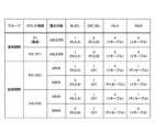
- FIG. 5 is a diagram illustrating an example of the operation of the control circuit 210 in the first embodiment of the present technology.
- One of two pixels (pixels 301 and 302) in pixel block 300 is designated as pixel A, and the other is designated as pixel B.
- the control circuit 210 sets the selection signal IN_SEL to "1" and the selection signal CNT_SEL to "0". As a result, pixel A selects pulse signal PLS_A, and pixel B selects pulse signal PLS_B. Further, the control circuit 210 sets both enable signals EN_A and EN_B to "0" (ie, enable). With these controls, both pixels A and B are exposed.
- the control circuit 210 sets the selection signal IN_SEL to "1" and sets the selection signal CNT_SEL to "1". As a result, the pulse signal PLS_A is selected in the pixel A, and the carry flag CF is selected in the pixel B. Further, the control circuit 210 sets the enable signal EN_A to "0" (enable) and sets the enable signal EN_B to "1" (ie, disable).
- the control circuit 210 sets the selection signal IN_SEL to "0” and sets the selection signal CNT_SEL to "1". As a result, the pulse signal PLS_B is selected in the pixel A, and the carry flag CF is selected in the pixel B. Further, the control circuit 210 sets the enable signal EN_A to "1” (disable) and sets the enable signal EN_B to "0" (enable).
- FIG. 6 is a diagram illustrating an example of the state of the pixel block 300 in the low-light mode in the first embodiment of the present technology.
- multiplexer 351 selects pulse signal PLS_A
- multiplexer 352 selects pulse signal PLS_B.
- the counter 360 counts in synchronization with the output signal OUT_A (ie, pulse signal PLS_A)
- the counter 370 counts in synchronization with the output signal OUT_B (ie, pulse signal PLS_B).
- the number of pulses for each pixel is counted. Assuming that the resolution of the counter for each pixel is N bits (N is an integer), the maximum value of each count value is 2N .
- FIG. 7 is a diagram illustrating an example of the state of a pixel block when pixel A is exposed in high-intensity mode in the first embodiment of the present technology.
- multiplexer 351 selects pulse signal PLS_A during the exposure period of pixel A
- multiplexer 352 selects carry flag CF from counter 360.
- the counter 360 counts in synchronization with the output signal OUT_A (pulse signal PLS_A)
- the counter 370 counts in synchronization with the output signal OUT_B (ie, carry flag CF).
- FIG. 8 is a diagram illustrating an example of the state of a pixel block when pixel B is exposed in high-intensity mode in the first embodiment of the present technology.
- multiplexer 351 selects pulse signal PLS_B and multiplexer 352 selects carry flag CF from counter 360 within the exposure period of pixel B. Further, the counter 360 counts in synchronization with the output signal OUT_A (pulse signal PLS_B), and the counter 370 counts in synchronization with the output signal OUT_B (ie, carry flag CF).
- counters 360 and 370 are connected in series, and when an overflow occurs in the preceding counter 360, the subsequent counter 370 counts. In this manner, counters 360 and 370 are shared by two pixels in pixel block 300 during high illuminance.
- the signal processing unit 230 At high illuminance, the signal processing unit 230 generates a 2N-bit digital signal for each of pixels A and B, with the output of the counter 360 (digital signal CNT_A) as the upper bit string and the output of the counter 370 (digital signal CNT_B) as the lower bit string. get.
- the resolution of the counter for each pixel is expanded to 2N bits, and the maximum value of each count value is expanded to 22N . This makes it possible to expand the dynamic range and improve the image quality of image data during high illuminance.
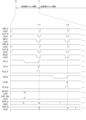
- FIG. 9 is a timing chart showing an example of the operation of the solid-state image sensor 200 in the low-light mode in the first embodiment of the present technology. It is assumed that the low illuminance mode is set at timing T0.
- the control circuit 210 sets enable signals EN_A and EN_B to high level, sets selection signal IN_SEL to high level, and sets selection signal CNT_SEL to low level.
- a pulse signal PLS_A is generated at timing T1, etc., and the counter 360 counts up the digital signal CNT_A in synchronization with the pulse signal.
- a pulse signal PLS_B is generated at timing T2 or the like, and the counter 370 counts up the digital signal CNT_B in synchronization with the pulse signal. As illustrated in the figure, in the low illuminance mode, two pixels are exposed at the same time, and the number of pulses is counted in parallel for each pixel.
- FIG. 10 is a timing chart showing an example of the operation of the solid-state image sensor in high-illuminance mode in the first embodiment of the present technology. It is assumed that the high illuminance mode is set at timing T10. It is assumed that pixel A is exposed within a period from timing T10 to T12, and pixel B is exposed within a period from timing T12 to T14. Similarly, after timing T14, pixels A and B are exposed alternately.
- the control circuit 210 sets the enable signal EN_A to a high level and sets the enable signal EN_B to a low level. Furthermore, the control circuit 210 sets the selection signals IN_SEL and CNT_SEL to high level. Pulse signal PLS_A is generated after timing T10, and counter 360 counts up digital signal CNT_A in synchronization with the pulse signal.
- the counter 370 counts up the digital signal CNT_B in synchronization with the carry flag.
- the control circuit 210 sets the enable signal EN_A to a low level and sets the enable signal EN_B to a high level. Further, the control circuit 210 sets the selection signal IN_SEL to a low level and sets the selection signal CNT_SEL to a high level. Pulse signal PLS_B is generated after timing T12, and counter 360 counts up digital signal CNT_A in synchronization with the pulse signal.
- the counter 370 counts up the digital signal CNT_B in synchronization with the carry flag.
- FIG. 11 is a flowchart illustrating an example of the operation of the solid-state image sensor 200 in the first embodiment of the present technology. This operation is started, for example, when low light mode is set.
- a counter within each pixel counts the number of pulses for all pixels (step S901).
- the signal processing unit 230 performs signal processing to generate a frame (step S902).
- a circuit outside the pixel determines whether the illumination is high based on the frame (step S903). For example, when the total value or average value of the count values of all pixels is greater than or equal to a threshold value, it is determined that the illuminance is high.
- step S903 If the illuminance is not high (step S903: No), the solid-state image sensor 200 sets the low illuminance mode and executes step S901 and subsequent steps.
- step S903 if the illuminance is high (step S903: Yes), the solid-state image sensor 200 sets the high illuminance mode, and the counter in the pixel counts the number of pulses at pixel A (step S904). Next, in pixel B, a counter within that pixel counts the number of pulses (step S905). The signal processing unit 230 performs signal processing to generate a frame (step S906). After step S906, the solid-state image sensor 200 repeats steps S903 and subsequent steps.
- the solid-state image sensor 200 determines whether the illuminance is high for each frame, but the configuration is not limited to this, and the solid-state image sensor 200 determines whether the illuminance is high when two or more frames are captured after changing the mode. It is also possible to determine whether or not.
- the counter 370 counts in synchronization with the carry flag from the counter 360 in the high illuminance mode, so the dynamic range can be expanded during high illuminance.
- Second embodiment> In the first embodiment described above, the circuit outside the pixel determines whether or not the illuminance is high, but this determination can also be made within the pixel.
- the solid-state image sensor 200 in the second embodiment differs from the first embodiment in that a determiner for determining whether or not the illuminance is high is arranged within the pixel block 300.
- FIG. 12 is a circuit diagram showing a configuration example of a pixel block 300 in the second embodiment of the present technology.
- the pixel block 300 of this second embodiment differs from the first embodiment in that it further includes a determiner 380.
- the determiner 380 is shared by two pixels in the pixel block 300.
- the digital signals CNT_A and CNT_B from the counters 360 and 370 are input to the determiner 380.
- This determiner 380 determines whether the illuminance is high or not based on these digital signals.
- the determiner 380 calculates the total value or average value of the count values of all pixels or some representative pixels (pixels near the center, etc.) in the pixel block 300, and the value is greater than or equal to the threshold value. It is determined that the illuminance is high if it is, and it is determined that the illuminance is low if it is less than the threshold.
- the determiner 380 determines for each pixel whether the count value is greater than or equal to the threshold value, and determines the illuminance based on the results.
- the determiner 380 determines that the illuminance is high if the number of pixels whose count value is greater than or equal to the threshold value is equal to or greater than the number of pixels whose count value is less than the threshold value.
- the determiner 380 determines that the illuminance is low if the number of pixels whose count value is less than the threshold value is greater than or equal to the number of pixels whose count value is greater than or equal to the threshold value.
- the determiner 380 determines that the illuminance is high when one or more pixels have a count value equal to or greater than the threshold value.
- the determiner 380 determines that the illuminance is low when the number of pixels whose count value is less than the threshold value is one or more.
- the determiner 380 controls enable signals EN_A and EN_B and selection signals IN_SEL and CNT_SEL based on the determination result.
- the method of controlling these signals is the same as in the first embodiment.
- each pixel block 300 since it is determined whether each pixel block 300 has high illuminance, appropriate control can be performed according to the illuminance of each pixel.
- FIG. 13 is an example of a timing chart when switching from low-illuminance mode to high-illuminance mode in the second embodiment of the present technology. Assume that the above-mentioned (2-3) is used as a method for determining whether the illuminance is high. It is assumed that the low illuminance mode is set for the pixel block 300 of interest, and the count value (CNT_B) of pixel B becomes equal to or greater than the threshold value at timing T0.
- the determiner 380 determines that the illuminance is high, and switches to the high illuminance mode at timing T1 after reading out the count value. In the high-illuminance mode, pixel A is exposed from timing T1 to T2, and pixel B is exposed after timing T2. Note that the illuminance is determined individually for each pixel block other than the pixel block of interest.
- FIG. 14 is an example of a timing chart when switching from high-illuminance mode to low-illuminance mode in the second embodiment of the present technology. It is assumed that the high-illuminance mode is set for the pixel block 300 of interest, and that each count value (CNT_A and CNT_B) of pixels A and B is less than the threshold value. The determiner 380 determines that the illuminance is low, and switches to the low illuminance mode at timing T10.
- the determiner 380 compares the count value and the threshold value, but in this configuration, the higher the resolution of the counters 360 and 370, the larger the circuit scale of the determiner 380 becomes. There is a risk.
- the solid-state image sensor 200 in the third embodiment differs from the second embodiment in that the determiner 380 determines whether the illuminance is high or not based on a specific bit of the digital signal.
- FIG. 15 is a circuit diagram showing a configuration example of a pixel block 300 in the third embodiment of the present technology.
- the pixel block 300 of this third embodiment differs from the second embodiment in that counters 360 and 370 supply specific bits of the digital signal to a determiner 380.
- the n-th bits QAn and QBn are output.
- the determiner 380 determines whether the illuminance is high or not based on those bits. Depending on whether each of QAn and QBn is "1", it is determined whether the count value is equal to or greater than the threshold value 2n .
- the circuit scale of the determiner 380 can be reduced compared to the first embodiment. Furthermore, the number of wires from the counters 360 and 370 to the determiner 380 can be reduced compared to the second embodiment.
- the counters 360 and 370 may supply not specific bits but higher-order bits (such as the upper 2 bits of 4 bits) to the determiner 380, and the determiner 380 may make a determination based on those bits. can.
- FIG. 16 is an example of a timing chart when switching from low-illuminance mode to high-illuminance mode in the third embodiment of the present technology. Assume that the above-mentioned (2-3) is used as a method for determining whether the illuminance is high. It is assumed that the low illuminance mode is set for the pixel block 300 of interest, and the count value (CNT_B) of pixel B becomes "1" with QAn at timing T0.
- the determiner 380 determines that the illuminance is high, and switches to the high illuminance mode at timing T1 after reading the count value. In the high-illuminance mode, pixel A is exposed from timing T1 to T2, and pixel B is exposed after timing T2.
- FIG. 17 is an example of a timing chart when switching from high-illuminance mode to low-illuminance mode in the third embodiment of the present technology. It is assumed that the high-illuminance mode is set for the pixel block 300 of interest, and both QAn and QBn are "0". Since all of the count values are less than the threshold 2n , the determiner 380 determines that the illuminance is low, and switches to the low illuminance mode at timing T10.
- the determiner 380 determines whether or not the illuminance is high based on the specific bits from the counters 360 and 370.
- the circuit scale of the determiner 380 can be reduced more than the configuration.
- FIG. 18 is a diagram showing an example arrangement of each pixel within the pixel block 300 in the fourth embodiment of the present technology.
- a plurality of pixels are arranged in a Bayer array.
- a color filter (not shown) and a microlens (not shown) are arranged for each pixel.
- the color filter transmits any of the colors red, green, and blue.
- the pixels on which the color filters of each color are arranged are referred to as an r pixel, a g pixel, and a b pixel, respectively.
- two g pixels are arranged diagonally in two rows and two columns, and the rest are r pixels and b pixels.
- r pixel 303, g pixel, r pixel 304, and g pixel are arranged in the column direction.
- a sensor section 310, a multiplexer 351, and a counter 360 are arranged in the r pixel 303, and a sensor section 330, a multiplexer 352, and a counter 370 are arranged in the r pixel 304.
- the count value of each pixel can be made to be approximately the same.
- two pixels of the same color can also be arranged in the pixel block 300 in a quad Bayer arrangement.
- the second or third embodiment can be applied to the fourth embodiment.
- the determiner 380 can accurately determine the illuminance.
- the count values of each pixel can be made to be approximately the same.
- a microlens was arranged for each pixel, but in order to realize image plane phase difference AF (Auto Focus) in this configuration, in addition to the r pixel, g pixel, and b pixel, a microlens is arranged for each pixel. Furthermore, it is necessary to further arrange pixels for phase difference detection.
- the solid-state image sensor 200 in this fifth embodiment differs from the fourth embodiment in that a plurality of pixels are arranged directly under the microlens.
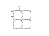
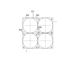
- FIG. 20 is a diagram showing an example arrangement of each pixel within the pixel block 300 in the fifth embodiment of the present technology.
- pixels are arranged in a quad Bayer array.
- a microlens 221 is arranged for every four adjacent pixels of the same color to guide incident light to those pixels.
- Multiple pixels at the bottom of microlens 221 (such as r pixels 303 and 304) share counters 360 and 370.
- the circuit at the subsequent stage of the pixel calculates the difference between the peaks of the image in which pixel signals are arranged on the left side (or upper side) of the microlens 221 and the image on which the pixel signals are arranged on the right side (or lower side) of the microlens 221.
- the distance is detected as a phase difference.
- a focus lens (not shown) is driven according to the phase difference. Thereby, image plane phase difference AF can be realized without arranging pixels for phase difference detection.
- the two pixels that share the counters 360 and 370 are arranged below the microlens 221, so that image plane phase difference AF can be easily realized.
- the count period of the pulse signal is kept constant, but this count period can also be changed during imaging.
- the solid-state imaging device 200 in this sixth embodiment differs from the first embodiment in that the count period is switched during imaging.
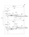
- FIG. 21 is a circuit diagram showing a configuration example of a pixel block 300 in the sixth embodiment of the present technology.
- the sensor section 310 includes a recharge transistor 321, a clip transistor 322, a SPAD 313, pMOS transistors 323 and 324, an nMOS transistor 325, and a buffer 326.
- the sensor section 330 includes a recharge transistor 341, a clip transistor 342, and a SPAD 333, pMOS transistors 343 and 344, an nMOS transistor 345, and a buffer 346.
- the recharge transistor 321 and the clip transistor 322 are connected in series between the cathode of the SPAD 313 and the power supply voltage VDD, with the recharge transistor 321 on the power supply side.
- the recharge transistor 321 performs recharging to return the cathode potential of the SPAD 313 to the power supply voltage VDD in accordance with the control signal XRE_A from the control circuit 210.
- the count period which is the interval at which recharging is performed, is controlled by the control circuit 210. If one or more photons are incident within this count period, one pulse is generated.
- the clip transistor 322 disconnects the SPAD 313 from the connection node between the recharge transistor 321 and the clip transistor 322 in accordance with the control signal CLP_A from the control circuit 210.
- the SPAD 313 is disconnected from the connection node immediately before the start of recharge, and the SPAD 313 is connected to that node within the recharge period. This clip transistor 322 allows reduction of cathode capacitance.
- the pMOS transistors 323 and 324 and the nMOS transistor 325 are connected in series between the power supply voltage VDD and the ground node, with the pMOS transistor 323 on the power supply side and the nMOS transistor 325 on the ground side.
- a control signal INI_A from the control circuit 210 is input to the gates of the pMOS transistor 323 and the nMOS transistor 325. Further, the gate of the pMOS transistor 324 is connected to a connection node between the recharge transistor 321 and the clip transistor 322.
- the buffer 326 outputs a signal of the potential of the connection node between the pMOS transistor 324 and the nMOS transistor 325 to the multiplexer 351 as a pulse signal PLS_A. Note that a two-stage inverter can be inserted instead of the buffer 326.
- the circuit configuration of the sensor section 330 is similar to that of the sensor section 310. However, control signals XRE_B, CLP_B and INI_B are input.
- the control circuit 210 controls the count cycle to either a long cycle longer than a predetermined time or a short cycle shorter than the predetermined time. By switching the count period during imaging, the number of pulses can be counted even when the frequency of light is higher than in the first embodiment. Furthermore, if the frequencies are the same, the count value can be made smaller than in the first embodiment. Therefore, the number of bits of digital signals and power consumption can be reduced.
- FIG. 22 is a diagram illustrating an example of the operation of the control circuit 210 in the sixth embodiment of the present technology.
- the control circuit 210 sets the selection signal IN_SEL to "1" and sets the selection signal CNT_SEL to "0".
- pixel A selects pulse signal PLS_A
- pixel B selects pulse signal PLS_B.
- the control circuit 210 sets both enable signals EN_A and EN_B to "0" (enable). With these controls, both pixels A and B are exposed.
- the control circuit 210 sets the selection signal IN_SEL to "1" and sets the selection signal CNT_SEL to "1". As a result, the pulse signal PLS_A is selected in the pixel A, and the carry flag CF is selected in the pixel B. Further, the control circuit 210 sets the enable signal EN_A to "0" (enable) and sets the enable signal EN_B to "1" (disable).
- the control circuit 210 sets the selection signal IN_SEL to "0” and sets the selection signal CNT_SEL to "1". As a result, the pulse signal PLS_B is selected in the pixel A, and the carry flag CF is selected in the pixel B. Further, the control circuit 210 sets the enable signal EN_A to "1” (disable) and sets the enable signal EN_B to "0" (enable).
- FIG. 23 is a timing chart showing an example of the operation of the solid-state image sensor 200 during the long-cycle count period in the sixth embodiment of the present technology.
- the count cycle is controlled to be a long cycle within the period from timing T0 to T1.
- control signal XRE_A is controlled to low level, and the first recharge is performed.
- second and third recharges are performed. After that, recharging is repeated periodically.
- These recharge intervals ie, count periods) are controlled to be long periods.
- the control circuit 210 sets the selection signal IN_SEL to high level and sets the selection signal CNT_SEL to low level.
- the digital signals CNT_A and CNT_B count up every count period when a photon is incident.
- FIG. 24 is a timing chart showing an example of the operation of the solid-state image sensor during the exposure period of pixel A in the short cycle count period in the sixth embodiment of the present technology.
- the count period is controlled to be short.
- the short cycle count period is controlled to be, for example, 10% or less of the total period.
- the control circuit 210 sets the selection signal IN_SEL to high level, sets the selection signal CNT_SEL to high level, and enables only pixel A with the enable signal.
- the digital signal CNT_A counts up every count period when a photon is incident.
- FIG. 25 is a timing chart showing an example of the operation of the solid-state image sensor during the exposure period of pixel B in the short cycle count period in the sixth embodiment of the present technology.
- the control circuit 210 sets the selection signal IN_SEL to a low level, sets the selection signal CNT_SEL to a high level, and enables only the pixel B using the enable signal.
- the digital signal CNT_B counts up every count period when a photon is incident.
- the count period is switched, the number of bits of the digital signal and the power consumption can be reduced compared to the case where the count period is not switched.
- the solid-state imaging device 200 switches the count cycle to one of two cycles, but it can also switch to one of three or more cycles.
- the solid-state imaging device 200 in this modification of the sixth embodiment differs from the sixth embodiment in that the count period is switched to one of three or more periods.
- FIG. 26 is a diagram illustrating an example of the operation of the control circuit 210 in a modification of the sixth embodiment of the present technology.
- the count period is switched to one of three or more periods.
- the count period is switched to any one of periods P1, P2, P3, and P4. It is assumed that P1 is the longest, P2 is shorter than P1, P3 is shorter than P2, and P4 is the shortest.
- P1 and P2 be a long period group
- P3 and P4 be a short period group
- P1 may be a long-period group
- P2, P3, and P4 may be short-period groups.
- the control circuit 210 When switching the count period to one of the long period groups, the control circuit 210 sets the selection signal IN_SEL to "1" and the selection signal CNT_SEL to “0". The control circuit 210 also exposes both pixels A and B. On the other hand, when switching the count period to one of the short period groups, the control circuit 210 sets the selection signal IN_SEL to "1” and the selection signal CNT_SEL to "1". Further, the control circuit 210 exposes only one of the pixels A and B, and switches the exposure target at regular intervals.
- the count cycle can be switched to any of three or more cycles.
- the control circuit 210 controls the count period to either a long period or a short period, but when the illuminance is high and the pulse number is counted in a long period, the count value becomes saturated. There is a risk of
- the solid-state image sensor 200 in the seventh embodiment differs from the sixth embodiment in that counting is enabled or disabled when the count period is long based on the digital signals of pixels A and B. .
- FIG. 27 is a circuit diagram showing an example of the configuration of the pixel block 300 in the seventh embodiment of the present technology.
- the pixel block 300 of the seventh embodiment differs from the sixth embodiment in that it further includes resistance elements 328 and 348, OR (logical sum) gates 327 and 347, and a determiner 381.
- the resistance element 328 is inserted between the SPAD 313 and the clip transistor 322, and the resistance element 348 is inserted between the SPAD 333 and the clip transistor 342. These resistance elements are inserted as necessary.
- the determiner 381 determines whether or not to enable counting of each of the counters 360 and 370 within a period where the count period is a long period, based on the digital signals CNT_A and CNT_B within a period where the count period is a short period. It is something.
- the selection signal CNT_SEL from the control circuit 210 and the digital signals CNT_A and CNT_B from the counters 360 and 370 are input to the determiner 381.
- This determiner 381 obtains digital signals CNT_A and CNT_B generated during a period in which the selection signal CNT_SEL is at a high level (that is, the count period is short). Then, the determiner 381 determines whether or not the illuminance is high based on these digital signals.
- the determiner 381 determines the illuminance using any of the determination methods (1), (2-1), and (2-3) described above.
- the determiner 381 determines that the illuminance is high when there is one or more pixels in which the value of the upper bit of the digital signal is greater than or equal to the threshold value.
- the determiner 381 determines that the illuminance is high when there is one or more pixels in which the value of the most significant bit (MSB: Most Significant Bit) of the digital signal is at a high level.
- the determiner 381 supplies an enable signal DIS to the OR gates 327 and 347.
- the enable signal DIS is controlled to a low level (enabled) during a period in which the count cycle is short. This enables counting of counters 360 and 370.
- the determiner 381 When determining that the illuminance is high, the determiner 381 sets the enable signal DIS to a high level (disabled) within a period in which the selection signal CNT_SEL is at a high level (that is, the count period is short). This invalidates the counts of counters 360 and 370 during a period in which the count cycle is long. On the other hand, when determining that the illuminance is low, the determiner 381 leaves the enable signal DIS at a low level and enables the counting of the counters 360 and 370.
- FIG. 28 is a timing chart showing an example of the operation of the solid-state image sensor 200 during the exposure period of pixel A in the short-cycle count period in the seventh embodiment of the present technology.
- FIG. 29 is a timing chart showing an example of the operation of the solid-state image sensor 200 during the exposure period of pixel B in the short-cycle count period in the seventh embodiment of the present technology.
- the same control as in the sixth embodiment is performed. Further, during a period in which the count cycle is short, the counts of the counters 360 and 370 are effectively controlled by the enable signal DIS at a low level (enable).
- FIG. 30 is a timing chart showing an example of the operation of the solid-state image sensor during the long-cycle count period in the seventh embodiment of the present technology. It is assumed that the determiner 381 determines that the illuminance is high based on a digital signal within a short cycle period. In this case, the determiner 381 sets the enable signal DIS to a high level (disable). As a result, as illustrated in the figure, the counts of the counters 360 and 370 are invalidated during a period in which the count period is a long period.
- the determiner 381 determines whether or not to enable counting of each of the counters 360 and 370 within a period when the count period is short, based on the digital signals CNT_A and CNT_B during the period when the count period is long. It is also possible to judge. In this case, counting within a short cycle period is disabled during low illuminance. Whether or not the illuminance is low is determined by any of the determination methods (1), (2-2), and (2-4) described above.
- the determiner 381 determines that the illuminance is low when there is one or more pixels in which the value of the upper bit of the digital signal within the long count period is less than the threshold value.
- the determiner 381 determines that the illuminance is low when there is one or more pixels in which the MSB value of the digital signal becomes low level within a period with a long count cycle.
- the fourth or fifth embodiment can be applied to the seventh embodiment.
- a modification of the sixth embodiment can be applied to the seventh embodiment.
- the determiner 381 enables or disables counting within a period with a long counting cycle based on the digital signals CNT_A and CNT_B. Numerical saturation can be prevented.
- the control circuit 210 controls the count cycle to either a long cycle or a short cycle, but the count cycle is switched within a 1V period for imaging one frame. You can.
- the solid-state imaging device 200 in this eighth embodiment differs from the sixth embodiment in that the count period is switched within a 1V period. Note that the 1V period is an example of a frame period described in the claims.
- FIG. 31 is a diagram illustrating an example of a count cycle within a 1V period of a predetermined row in the eighth embodiment of the present technology.
- the control circuit 210 switches the count period within a 1V period from timing T0 to T4.
- the count cycle is controlled to be a long cycle within the period from timing T0 to T1. Then, the control circuit 210 switches the count period to a short period at timing T1. Pixel A is exposed within a period from timing T1 to T2, and pixel B is exposed within a period from timing T2 to T3. The control circuit 210 switches the count period to a long period at timing T3. Thereafter, similar control is repeatedly executed until timing T4.
- the signal processing unit 230 acquires long-cycle and short-cycle digital signals for each pixel within a 1V period.
- the signal processing unit 230 calculates the statistics (average value and total value) of each digital signal in each period as a pixel signal for each pixel, and outputs a frame in which these pixel signals are arranged.
- each of the fourth, fifth, and seventh embodiments can be applied to the eighth embodiment. Further, a modification of the sixth embodiment can be applied to the eighth embodiment.
- control circuit 210 since the control circuit 210 switches the count period within the 1V period, blur can be suppressed.
- the control circuit 210 switches the count period within a 1V period, but at this time, exposure can be controlled using a rolling shutter method.
- the solid-state image sensor 200 in this ninth embodiment differs from the eighth embodiment in that exposure is controlled by a rolling shutter method.
- FIG. 32 is a timing chart showing an example of exposure and readout operations of the solid-state image sensor 200 in the ninth embodiment of the present technology. It is assumed that two pixels sharing counters 360 and 370 are arranged in a column direction, for example.
- the control circuit 210 sequentially selects a plurality of rows in the pixel array section 220 and starts exposure by resetting the counter. During exposure, the signal processing unit 230 reads only the most significant bit (MSB) of the digital signal of the selected row a predetermined number of times during exposure.
- MSB most significant bit
- control circuit 210 sequentially selects a plurality of rows in the pixel array section 220 and stops the counter, thereby ending the exposure.
- the signal processing unit 230 sequentially reads digital signals from each of the plurality of rows. Furthermore, the control circuit 210 switches the count period within the 1V period.
- the count period on the first line is controlled to be a long period within the period from timing T1 to T8, and the count period on the second line is controlled to be a long period within the period from timing T2 to T9 immediately after timing T1. controlled by.
- the first row is exposed from timing T1 to T7.
- the second row is exposed from timing T2 to T8. In this way, a rolling shutter method is used that sequentially exposes each row.
- the MSB of the first row is read from timing T3 to T4 and from timing T5 to T6 during exposure.
- the MSB of the second row is read in a predetermined period from timing T4 and a predetermined period from timing T6. All bits of the digital signal on the first row are read out within the period from timing T7 to T8, and all bits of the digital signal on the second row are read out within the period from timing T8 to T9.
- the control circuit 210 switches the counter cycles of the first and second rows to short cycles.
- Pixel A (in other words, the first row) is exposed within the period from timing T9 to T10, and all bits of that row are read out within the period from timing T10 to T11.
- the MSB of the first row is read out.
- Pixel B (in other words, the second row) is exposed within the period from timing T11 to T12, and all bits of that row are read out within the period from timing T12 to T13. Further, during exposure, the MSB of the second row is read out a predetermined number of times.
- the signal processing unit 230 Based on each read MSB, the signal processing unit 230 obtains a bit string indicating the number of times the MSB changes from "1" to "0" (that is, the number of overflows) as the upper bits. Then, the signal processing unit 230 uses the bit string obtained by reading all the bits as the lower bits, and obtains a digital signal consisting of upper bits and lower bits for each pixel. This allows the number of bits of the digital signal to be expanded.
- the frame rate can be improved more than when using the global shutter method, which will be described later.
- each of the fourth, fifth, and seventh embodiments can be applied to the ninth embodiment. Further, a modification of the sixth embodiment can be applied to the ninth embodiment.
- the frame rate can be improved compared to the case of the global shutter method.
- FIG. 33 is a timing chart showing an example of exposure and readout operations of the solid-state image sensor 200 in the tenth embodiment of the present technology.
- the control circuit 210 simultaneously selects all rows (that is, all pixels) and starts exposure. Then, at timing T3 immediately before the end of the 1V period, the control circuit 210 selects all rows simultaneously and ends the exposure. From timing T3 to the end of the 1V period, the signal processing unit 230 sequentially reads out all bits of the digital signals of each of the plurality of rows.
- control circuit 210 switches the count period within the 1V period. Upon switching, the control circuit 210 controls exposure using a rolling shutter method. For example, at timing T1, the count period is switched to a short period, and rows including pixels A are sequentially exposed. After timing T2, rows including pixels B are sequentially exposed.
- the signal processing unit 230 sequentially reads the MSB of each row a predetermined number of times. At the end of exposure, the signal processing unit 230 sequentially reads out the digital signals of each row.
- each of the fourth, fifth, and seventh embodiments can be applied to the tenth embodiment. Further, a modification of the sixth embodiment can be applied to the tenth embodiment.
- control circuit 210 controls exposure using the global shutter method at the start and end of the 1V period, rolling shutter distortion can be suppressed.
- the control circuit 210 performs exposure control using a rolling shutter method in the middle of the 1V period, but this control may cause rolling shutter distortion.
- the solid-state image sensor 200 in the eleventh embodiment differs from the tenth embodiment in that exposure is controlled using a global shutter method even within the 1V period.
- FIG. 34 is a timing chart showing an example of exposure and readout operations of the solid-state image sensor 200 in the eleventh embodiment of the present technology.
- the control circuit 210 simultaneously selects all rows (all pixels) to start exposure, and at timing T1 within the 1V period, selects all pixels simultaneously and ends the exposure.
- the signal processing unit 230 sequentially reads out the MSB of each row a predetermined number of times. Then, from timing T1 to timing T2, the signal processing unit 230 sequentially reads out the digital signals of each row.
- the control circuit 210 switches the count period to a short period at timing T2, selects all the rows including the pixel A (that is, odd-numbered rows), and simultaneously starts exposure, and at timing T3, selects those rows simultaneously. to end the exposure.
- the signal processing unit 230 sequentially reads out the MSB of each row a predetermined number of times. Then, from timing T3 to timing T4, the signal processing unit 230 sequentially reads out the digital signals of each row.
- the control circuit 210 selects all of the rows (that is, even-numbered rows) including pixels B and starts exposure at the same time, and at timing T5, selects those rows simultaneously and ends the exposure.
- the signal processing unit 230 sequentially reads out the MSB of each row a predetermined number of times.
- the signal processing unit 230 sequentially reads out the digital signals of each row. After timing T6, similar control is repeatedly executed.
- each of the fourth, fifth, and seventh embodiments can be applied to the eleventh embodiment. Further, a modification of the sixth embodiment can be applied to the eleventh embodiment.
- control circuit 210 since the control circuit 210 controls exposure using the global shutter method even in the middle of the 1V period, rolling shutter distortion can be further suppressed.
- Twelfth embodiment In the eleventh embodiment described above, the control circuit 210 starts the next exposure after reading of all rows is completed, but with this configuration, it is difficult to further improve the frame rate.
- the solid-state image sensing device 200 according to the twelfth embodiment differs from the eleventh embodiment in that exposure and readout during a short cycle count period are performed in a complementary manner.
- FIG. 35 is a timing chart showing an example of exposure and readout operations of the solid-state image sensor 200 in the twelfth embodiment of the present technology.
- control up to timing T2 when the count period switches to a short cycle is the same as in the eleventh embodiment.
- signal lines (not shown) for transmitting digital signals to the signal processing section 230 are wired in the column direction. Each pixel A (or pixel B) in the column that shares this signal line is exposed in half.
- the control circuit 210 exposes half of the pixels A at the same time. Since the pixels A are arranged in odd-numbered rows, half of the odd-numbered rows (first row, fifth row, etc.) are exposed at the same time. Then, within the period from timing T4 to T5, the control circuit 210 simultaneously exposes the remaining half of the pixels A (the third row, the seventh row, etc.).
- the control circuit 210 simultaneously exposes half of the pixels B. Since the pixels B are arranged in even-numbered rows, half of the even-numbered rows (second row, sixth row, etc.) are exposed. Then, within the period from timing T8 to T9, the control circuit 210 exposes the remaining half of the pixels B (4th row, 8th row, etc.).
- the signal processing unit 230 sequentially reads the MSB of each row a predetermined number of times. Furthermore, within the period from timing T3 to timing T5, the signal processing unit 230 sequentially reads out half of the pixels A row by row. The remaining half of the pixel A can be exposed during these readout periods.
- the signal processing unit 230 sequentially reads out the remaining half of the pixels A row by row. Half of the pixel B can be exposed during these readout periods.
- the signal processing unit 230 sequentially reads out half of the pixels B row by row. The remaining half of the pixel B can be exposed during these readout periods. After timing T9, the signal processing unit 230 sequentially reads out the remaining half of the pixels B row by row.
- the frame rate can be further improved by exposing the remaining half of the pixel A (or pixel B) while reading out half of the pixel A (or pixel B).
- each of the fourth, fifth, and seventh embodiments can be applied to the twelfth embodiment. Further, a modification of the sixth embodiment can be applied to the twelfth embodiment.
- control circuit 210 exposes the remaining half, making it possible to further improve the frame rate. can.
- the solid-state image sensor 200 according to the thirteenth embodiment differs from the first embodiment in that pixel addition is performed.
- FIG. 36 is a circuit diagram showing a configuration example of a pixel block 300 in the thirteenth embodiment of the present technology.
- the pixel block 300 of the thirteenth embodiment differs from the first embodiment in that it further includes a logic gate that performs a logic operation for pixel addition.
- an OR gate 391 is used as a logic gate.
- the OR gate 391 outputs the logical sum of the pulse signals PLS_A and PLS_B to the multiplexer 351. Note that the logical operation on the two pulse signals is not limited to logical sum. If the pulse signal falls in response to the incidence of photons, an AND (logical product) gate is inserted in place of the OR gate 391. Alternatively, a logical difference can be calculated using a NOT gate instead of the OR gate 391.
- OR gate 391 is an example of the first logic gate described in the claims.
- FIG. 37 is a diagram illustrating an example of the operation of the control circuit 210 in the thirteenth embodiment of the present technology.
- one of a plurality of modes including addition mode and non-addition mode is set.
- the addition mode is a mode in which the respective pulse signals of two pixels in the pixel block 300 are added
- the non-addition mode is a mode in which these signals are not added.
- the control circuit 210 sets the selection signal IN_SEL to "1" and sets the selection signal CNT_SEL to "0". As a result, pixel A selects pulse signal PLS_A, and pixel B selects pulse signal PLS_B. Further, the control circuit 210 sets enable signals EN_A and EN_B to "0" (enable).
- the control circuit 210 sets the selection signal IN_SEL to "0" and the selection signal CNT_SEL to "1". As a result, in pixel A, the logical sum of pulse signals PLS_A and PLS_B is selected, and in pixel B, the carry flag is selected. Further, the control circuit 210 sets enable signals EN_A and EN_B to "0" (enable).
- each of the fourth and fifth embodiments can be applied to the thirteenth embodiment.
- a modification of the sixth embodiment can be applied to the thirteenth embodiment.
- the pixel block 300 since the pixel block 300 adds the pulse signals PLS_A and PLS_B in the addition mode, the sensitivity can be improved compared to the case of non-addition.
- the count period of the pulse signal is kept constant, but this count period can also be changed during imaging.
- the solid-state imaging device 200 according to the fourteenth embodiment differs from the thirteenth embodiment in that the count period is changed during imaging.
- FIG. 38 is a circuit diagram showing a configuration example of a pixel block 300 in the fourteenth embodiment of the present technology.
- the sensor section 310 includes a recharge transistor 321, a clip transistor 322, a SPAD 313, pMOS transistors 323 and 324, an nMOS transistor 325, and a buffer 326.
- the sensor section 330 includes a recharge transistor 341, a clip transistor 342, and a SPAD 333, pMOS transistors 343 and 344, an nMOS transistor 345, and a buffer 346.
- circuit configurations of these sensor units 310 and 330 are similar to the sixth embodiment illustrated in FIG. 21.
- control circuit 210 can switch the count period in the non-addition mode.
- the counters are connected in series as in the sixth embodiment, and the resolution of the counters is expanded.
- FIG. 39 is a timing chart showing an example of the operation of the solid-state image sensor 200 in the addition mode in the fourteenth embodiment of the present technology.
- the control circuit 210 sets the selection signal IN_SEL to a low level and sets the selection signal CNT_SEL to a high level. As a result, pixel A selects the logical sum, and pixel B selects the carry flag.
- the digital signal CNT_A counts up, and when the digital signal CNT_A is saturated at timing T3, the digital signal CNT_B counts up.
- each of the fourth, fifth, seventh to twelfth embodiments can be applied to the fourteenth embodiment. Further, a modification of the sixth embodiment can be applied to the fourteenth embodiment.
- the fourteenth embodiment of the present technology since the count period is switched in the non-addition mode, the number of bits of the digital signal and the power consumption can be reduced compared to the case where the count period is not switched. Can be done.
- the solid-state image sensor 200 adds two pixels, but it is also possible to add three or more pixels.
- the solid-state imaging device 200 in the fifteenth embodiment differs from the thirteenth embodiment in that four pixels are added.
- FIG. 40 is a diagram showing an example of arrangement of each pixel in the pixel block 300 in the fifteenth embodiment of the present technology.
- pixels are arranged in a quad Bayer arrangement.
- a microlens 221 is arranged for every four adjacent pixels of the same color to guide incident light to those pixels.
- the four pixels at the bottom of the microlens 221 (such as r pixels 303, 304, 305, and 306) share a counter.
- FIG. 41 is a circuit diagram showing a configuration example of a pixel block 300 in the fifteenth embodiment of the present technology.
- the pixel block 300 of the fifteenth embodiment includes multiplexers 353 to 356 instead of multiplexers 351 and 352, and further includes sensor sections 315 and 335, OR gates 392 and 393, and counters 365 and 375.
- the sensor unit 315 generates a pulse signal PLS_C in response to incident photons.
- the sensor unit 335 generates a pulse signal PLS_D in response to incident photons.
- the circuit configurations of these sensor sections are similar to the sensor section 310. Note that the sensor sections 315 and 335 are examples of the third and fourth sensor sections described in the claims.
- OR gate 392 outputs the logical sum of the pulse signals PLS_C and PLC_D to the multiplexer 355 and the OR gate 393.
- OR gate 393 outputs the logical sum of the respective outputs of OR gates 391 and 392 to multiplexer 353. Note that the logical operation on the two pulse signals is not limited to logical sum. If the pulse signal falls in response to the incidence of photons, AND gates are inserted in place of the OR gates 391 to 393. Alternatively, a logical difference can be calculated using a NOT gate instead of an OR gate.
- OR gates 392 and 393 are examples of the second and third logic gates described in the claims.
- the multiplexer 353 selects one of the logical sum of the OR gate 393, the pulse signal PLS_A, and the logical sum of the OR gate 391 according to the selection signal IN_SEL1 from the control circuit 210, and outputs it to the counter 360 as an output signal OUT_A. It is something. For example, when the selection signal IN_SEL1 is "2", the logical sum of the OR gate 393 is selected, when it is "1", the pulse signal PLS_A is selected, and when the selection signal IN_SEL1 is "0", the logical sum of the OR gate 391 is selected. Ru. Note that the multiplexer 353 is an example of a first multiplexer described in the claims.
- the counter 360 of the fifteenth embodiment supplies the carry flag as CF_A to the multiplexer 354.
- the multiplexer 354 selects either the carry flag CF_A or the pulse signal PLS_B according to the selection signal CNT_SEL1 from the control circuit 210, and outputs it to the counter 370 as an output signal OUT_B. For example, when selection signal CNT_SEL1 is "1”, carry flag CF_A is selected, and when selection signal CNT_SEL1 is "0", pulse signal PLS_B is selected. Note that the multiplexer 354 is an example of a second multiplexer described in the claims.
- the counter 370 of the fifteenth embodiment further generates a carry flag and supplies it to the multiplexer 355 as CF_B.
- the multiplexer 355 selects one of the carry flag CF_B, the pulse signal PLS_C, and the logical sum of the OR gate 392 according to the selection signal IN_SEL2 from the control circuit 210, and outputs it to the counter 365 as an output signal OUT_C. .
- the selection signal IN_SEL2 is "2”
- the carry flag CF_B is selected, when it is "1”
- the pulse signal PLS_C is selected, and when it is "0”
- the logical sum of the OR gate 392 is selected.
- the multiplexer 355 is an example of a third multiplexer described in the claims.
- the counter 365 counts a count value in synchronization with the output signal OUT_C, and outputs a digital signal CNT_C indicating the count value to the signal processing section 230. Further, this counter 365 generates a carry flag CF_C indicating whether or not an overflow has occurred, and outputs it to the multiplexer 356. Note that the counter 365 is an example of a third counter described in the claims.
- the multiplexer 356 selects either the carry flag CF_C or the pulse signal PLS_D according to the selection signal CNT_SEL2 from the control circuit 210, and outputs it to the counter 375 as an output signal OUT_D. For example, when selection signal CNT_SEL2 is "1", carry flag CF_C is selected, and when selection signal CNT_SEL2 is "0", pulse signal PLS_D is selected. Note that the multiplexer 356 is an example of a fourth multiplexer described in the claims.
- the counter 375 counts a count value in synchronization with the output signal OUT_D, and outputs a digital signal CNT_D indicating the count value to the signal processing section 230. Note that the counter 375 is an example of a fourth counter described in the claims.
- the pixel block 300 in the figure functions as the r pixels 303 to 306 illustrated in FIG. 40.
- FIG. 42 is a diagram illustrating an example of the operation of the control circuit 210 in the fifteenth embodiment of the present technology.
- one of a plurality of modes including a non-addition mode, a two-pixel addition mode, and a four-pixel addition mode is set.
- the 2-pixel addition mode is a mode in which two pixels each out of the four pixels in the pixel block 300 are added
- the 4-pixel addition mode is a mode in which all four pixels are added.
- the non-addition mode is a mode in which each pixel is not added. Note that the configuration may be such that the addition mode can be switched between one of the 2-pixel addition mode and the 4-pixel addition mode.
- the control circuit 210 sets the selection signal IN_SEL1 to “1", the selection signal CNT_SEL1 to “0”, the selection signal IN_SEL2 to “1", and the selection signal CNT_SEL2 to "0". .
- multiplexer 353 selects pulse signal PLS_A
- multiplexer 354 selects pulse signal PLS_B
- multiplexer 355 selects pulse signal PLS_C
- multiplexer 356 selects pulse signal PLS_D.
- the control circuit 210 sets the enable signals of all pixels to "0" (enable).
- the control circuit 210 sets the selection signal IN_SEL1 to “0”, sets the selection signal CNT_SEL1 to “1”, sets the selection signal IN_SEL2 to “0”, and sets the selection signal CNT_SEL2 to “1”. ”.
- multiplexer 353 selects the logical sum of pulse signals PLS_A and PLS_B, and multiplexer 354 selects carry flag CF_A.
- Multiplexer 355 selects the logical sum of pulse signals PLS_C and PLS_D, and multiplexer 356 selects carry flag CF_C. Further, the control circuit 210 sets the enable signals of all pixels to "0" (enable).
- the control circuit 210 sets the selection signal IN_SEL1 to “2", the selection signal CNT_SEL1 to “1”, the selection signal IN_SEL2 to “2”, and the selection signal CNT_SEL2 to "1”. ”.
- multiplexer 353 selects the logical sum of pulse signals PLS_A, PLS_B, PLS_C, and PLS_D, and multiplexer 354 selects carry flag CF_A.
- Multiplexer 355 selects carry flag CF_B, and multiplexer 356 selects carry flag CF_C.
- the control circuit 210 sets the enable signals of all pixels to "0" (enable).
- the circuit at the subsequent stage of the pixel (signal processing unit 230, etc.) generates an image in which pixel signals are arranged on the left side (or upper side) of each microlens 221, and an image where pixel signals are arranged on the right side (or lower side) of each microlens 221.
- the distance between each peak is detected as a phase difference.
- a focus lens (not shown) is driven according to the phase difference. Thereby, image plane phase difference AF can be realized.
- the pixel block 300 adds the pulse signals PLS_A, PLS_B, PLS_C, and PLS_D in the four-pixel addition mode, so that sensitivity can be further improved.
- the resolution of the counter is kept constant in the non-addition mode, but with this configuration, the resolution of the counter may be insufficient in the case of high illuminance.
- the solid-state image sensor 200 in the sixteenth embodiment differs from the thirteenth embodiment in that the resolution of the counter is expanded at high illumination in the non-addition mode.
- the circuit configuration of the pixel block 300 in the sixteenth embodiment is the same as that in the thirteenth embodiment illustrated in FIG. 36.
- FIG. 43 is a diagram illustrating an example of the operation of the control circuit 210 in the thirteenth embodiment of the present technology.
- any one of a plurality of modes including a non-additive low illuminance mode, a non-additive high illuminance mode, and an additive mode is set.
- the addition mode is a mode in which the respective pulse signals of two pixels in the pixel block 300 are added, and the non-addition low illuminance mode and the non-addition high illuminance mode are modes in which these signals are not added.
- non-additive low illuminance mode is a mode that is set when the illuminance is low, below a predetermined value
- non-additive high illuminance mode is a mode that is set when the illuminance is high, which is higher than a predetermined value
- control contents of the non-additional low-light mode of the sixteenth embodiment are similar to the control contents of the low-light mode of the first embodiment illustrated in FIG.
- the control contents of the non-additional high-intensity mode of the sixteenth embodiment are similar to the control contents of the high-intensity mode of the first embodiment illustrated in FIG.
- the control contents of the addition mode of the sixteenth embodiment are similar to the control contents of the addition mode of the thirteenth embodiment illustrated in FIG.
- the resolution of the counter is expanded during high illuminance in the non-addition mode, so the dynamic range can be expanded during high illuminance.
- the circuit within the solid-state image sensor 200 is arranged on a single semiconductor chip, but with this configuration, it is difficult to reduce the circuit scale for each chip.
- the solid-state imaging device 200 according to the seventeenth embodiment differs from the first embodiment in that circuits are distributed and arranged on two stacked chips.
- FIG. 44 is a circuit diagram showing a configuration example of the pixel block 300 in the seventeenth embodiment of the present technology.
- a solid-state image sensor 200 in this seventeenth embodiment includes a pixel chip 201 and a circuit chip 202 that are stacked. These chips are electrically connected through connections such as vias. Note that in addition to vias, connection can also be made by Cu--Cu junctions or bumps. Connection can also be made by other methods (magnetic coupling, etc.). Further, although two chips are stacked, three or more layers can also be stacked.
- SPADs 313 and 333 are arranged on the pixel chip 201, and the remaining circuits and elements are arranged on the circuit chip 202.
- the clip transistors 322 and 342 are arranged on the pixel chip 201 as illustrated in FIG. 45.
- the seventeenth embodiment of the present technology since the layered structure is adopted, it is possible to easily increase the number of pixels.
- the control circuit 210 causes all pixels in the pixel array section 220 to output pulse signals, but with this configuration, it is difficult to reduce the readout time and the amount of data. .
- the solid-state imaging device 200 according to the eighteenth embodiment differs from the first embodiment in that the control circuit 210 causes some pixels in the pixel array section 220 to output pulse signals.
- FIG. 46 is a diagram illustrating an example of a region to be controlled in the eighteenth embodiment of the present technology.
- a region 225 such as a ROI (Region of Interest) is set as a control target.
- the area 225 is set by a user's operation or by executing various applications.
- the control circuit 210 enables the pixels in the area 225 among all the pixels by an enable signal and causes them to output a pulse signal. As a result, the time required for reading and the amount of data to be read can be reduced compared to the case where all pixels are controlled.
- control circuit 210 causes some pixels to output pulse signals, so that the readout time and data amount can be reduced.
- the technology according to the present disclosure (this technology) can be applied to various products.
- the technology according to the present disclosure may be realized as a device mounted on any type of moving body such as a car, electric vehicle, hybrid electric vehicle, motorcycle, bicycle, personal mobility, airplane, drone, ship, robot, etc. You can.
- FIG. 47 is a block diagram illustrating a schematic configuration example of a vehicle control system, which is an example of a mobile body control system to which the technology according to the present disclosure can be applied.
- the vehicle control system 12000 includes a plurality of electronic control units connected via a communication network 12001.
- the vehicle control system 12000 includes a drive system control unit 12010, a body system control unit 12020, an outside vehicle information detection unit 12030, an inside vehicle information detection unit 12040, and an integrated control unit 12050.
- a microcomputer 12051, an audio/image output section 12052, and an in-vehicle network I/F (interface) 12053 are illustrated.
- the drive system control unit 12010 controls the operation of devices related to the drive system of the vehicle according to various programs.
- the drive system control unit 12010 includes a drive force generation device such as an internal combustion engine or a drive motor that generates drive force for the vehicle, a drive force transmission mechanism that transmits the drive force to wheels, and a drive force transmission mechanism that controls the steering angle of the vehicle. It functions as a control device for a steering mechanism to adjust and a braking device to generate braking force for the vehicle.
- the body system control unit 12020 controls the operations of various devices installed in the vehicle body according to various programs.
- the body system control unit 12020 functions as a keyless entry system, a smart key system, a power window device, or a control device for various lamps such as a headlamp, a back lamp, a brake lamp, a turn signal, or a fog lamp.
- radio waves transmitted from a portable device that replaces a key or signals from various switches may be input to the body control unit 12020.
- the body system control unit 12020 receives input of these radio waves or signals, and controls the door lock device, power window device, lamp, etc. of the vehicle.
- the external information detection unit 12030 detects information external to the vehicle in which the vehicle control system 12000 is mounted.
- an imaging section 12031 is connected to the outside-vehicle information detection unit 12030.
- the vehicle exterior information detection unit 12030 causes the imaging unit 12031 to capture an image of the exterior of the vehicle, and receives the captured image.
- the external information detection unit 12030 may perform object detection processing such as a person, car, obstacle, sign, or text on the road surface or distance detection processing based on the received image.
- the imaging unit 12031 is an optical sensor that receives light and outputs an electrical signal according to the amount of received light.
- the imaging unit 12031 can output the electrical signal as an image or as distance measurement information.
- the light received by the imaging unit 12031 may be visible light or non-visible light such as infrared rays.
- the in-vehicle information detection unit 12040 detects in-vehicle information.
- a driver condition detection section 12041 that detects the condition of the driver is connected to the in-vehicle information detection unit 12040.
- the driver condition detection unit 12041 includes, for example, a camera that images the driver, and the in-vehicle information detection unit 12040 detects the degree of fatigue or concentration of the driver based on the detection information input from the driver condition detection unit 12041. It may be calculated, or it may be determined whether the driver is falling asleep.
- the microcomputer 12051 calculates control target values for the driving force generation device, steering mechanism, or braking device based on the information inside and outside the vehicle acquired by the vehicle exterior information detection unit 12030 or the vehicle interior information detection unit 12040, Control commands can be output to 12010.
- the microcomputer 12051 realizes ADAS (Advanced Driver Assistance System) functions, including vehicle collision avoidance or shock mitigation, follow-up based on the following distance, vehicle speed maintenance, vehicle collision warning, vehicle lane departure warning, etc. It is possible to perform cooperative control for the purpose of ADAS (Advanced Driver Assistance System) functions, including vehicle collision avoidance or shock mitigation, follow-up based on the following distance, vehicle speed maintenance, vehicle collision warning, vehicle lane departure warning, etc. It is possible to perform cooperative control for the purpose of
- ADAS Advanced Driver Assistance System
- the microcomputer 12051 controls the driving force generating device, steering mechanism, braking device, etc. based on information about the surroundings of the vehicle acquired by the vehicle exterior information detection unit 12030 or the vehicle interior information detection unit 12040. It is possible to perform cooperative control for the purpose of autonomous driving, etc., which does not rely on operation.
- the microcomputer 12051 can output a control command to the body system control unit 12020 based on the information outside the vehicle acquired by the outside information detection unit 12030.
- the microcomputer 12051 controls the headlamps according to the position of the preceding vehicle or oncoming vehicle detected by the vehicle exterior information detection unit 12030, and performs cooperative control for the purpose of preventing glare, such as switching from high beam to low beam. It can be carried out.
- the audio and image output unit 12052 transmits an output signal of at least one of audio and images to an output device that can visually or audibly notify information to the occupants of the vehicle or to the outside of the vehicle.
- an audio speaker 12061, a display section 12062, and an instrument panel 12063 are illustrated as output devices.
- the display unit 12062 may include, for example, at least one of an on-board display and a head-up display.
- FIG. 48 is a diagram showing an example of the installation position of the imaging section 12031.
- the imaging unit 12031 includes imaging units 12101, 12102, 12103, 12104, and 12105.
- the imaging units 12101, 12102, 12103, 12104, and 12105 are provided, for example, at positions such as the front nose, side mirrors, rear bumper, back door, and the top of the windshield inside the vehicle 12100.
- An imaging unit 12101 provided in the front nose and an imaging unit 12105 provided above the windshield inside the vehicle mainly acquire images in front of the vehicle 12100.
- Imaging units 12102 and 12103 provided in the side mirrors mainly capture images of the sides of the vehicle 12100.
- An imaging unit 12104 provided in the rear bumper or back door mainly captures images of the rear of the vehicle 12100.
- the imaging unit 12105 provided above the windshield inside the vehicle is mainly used to detect preceding vehicles, pedestrians, obstacles, traffic lights, traffic signs, lanes, and the like.
- FIG. 47 shows an example of the imaging range of the imaging units 12101 to 12104.
- An imaging range 12111 indicates the imaging range of the imaging unit 12101 provided on the front nose
- imaging ranges 12112 and 12113 indicate imaging ranges of the imaging units 12102 and 12103 provided on the side mirrors, respectively
- an imaging range 12114 shows the imaging range of the imaging unit 12101 provided on the front nose.
- the imaging range of the imaging unit 12104 provided in the rear bumper or back door is shown. For example, by overlapping the image data captured by the imaging units 12101 to 12104, an overhead image of the vehicle 12100 viewed from above can be obtained.
- At least one of the imaging units 12101 to 12104 may have a function of acquiring distance information.
- at least one of the imaging units 12101 to 12104 may be a stereo camera including a plurality of image sensors, or may be an image sensor having pixels for phase difference detection.
- the microcomputer 12051 determines the distance to each three-dimensional object within the imaging ranges 12111 to 12114 and the temporal change in this distance (relative speed with respect to the vehicle 12100) based on the distance information obtained from the imaging units 12101 to 12104. In particular, by determining the three-dimensional object that is closest to the vehicle 12100 on its path and that is traveling at a predetermined speed (for example, 0 km/h or more) in approximately the same direction as the vehicle 12100, it is possible to extract the three-dimensional object as the preceding vehicle. can.
- a predetermined speed for example, 0 km/h or more
- the microcomputer 12051 can set an inter-vehicle distance to be secured in advance in front of the preceding vehicle, and perform automatic brake control (including follow-up stop control), automatic acceleration control (including follow-up start control), and the like. In this way, it is possible to perform cooperative control for the purpose of autonomous driving, etc., in which the vehicle travels autonomously without depending on the driver's operation.
- the microcomputer 12051 transfers three-dimensional object data to other three-dimensional objects such as two-wheeled vehicles, regular vehicles, large vehicles, pedestrians, and utility poles based on the distance information obtained from the imaging units 12101 to 12104. It can be classified and extracted and used for automatic obstacle avoidance. For example, the microcomputer 12051 identifies obstacles around the vehicle 12100 into obstacles that are visible to the driver of the vehicle 12100 and obstacles that are difficult to see. Then, the microcomputer 12051 determines a collision risk indicating the degree of risk of collision with each obstacle, and when the collision risk exceeds a set value and there is a possibility of a collision, the microcomputer 12051 transmits information via the audio speaker 12061 and the display unit 12062. By outputting a warning to the driver via the vehicle control unit 12010 and performing forced deceleration and avoidance steering via the drive system control unit 12010, driving support for collision avoidance can be provided.
- the microcomputer 12051 determines a collision risk indicating the degree of risk of collision with each obstacle, and when the collision risk exceed
- At least one of the imaging units 12101 to 12104 may be an infrared camera that detects infrared rays.
- the microcomputer 12051 can recognize a pedestrian by determining whether the pedestrian is present in the images captured by the imaging units 12101 to 12104.
- pedestrian recognition involves, for example, a procedure for extracting feature points in images captured by the imaging units 12101 to 12104 as infrared cameras, and a pattern matching process is performed on a series of feature points indicating the outline of an object to determine whether it is a pedestrian or not.
- the audio image output unit 12052 creates a rectangular outline for emphasis on the recognized pedestrian.
- the display unit 12062 is controlled to display the .
- the audio image output unit 12052 may control the display unit 12062 to display an icon or the like indicating a pedestrian at a desired position.
- the technology according to the present disclosure can be applied to, for example, the imaging unit 12031 among the configurations described above.
- the imaging device 100 in FIG. 1 can be applied to the imaging unit 12031.
- the present technology can also have the following configuration.
- a first counter that outputs a flag; and a second counter that counts a count value in synchronization with either the first carry flag or the second pulse signal and outputs a second digital signal indicating the count value.
- Device a first sensor unit that generates a first pulse signal in response to incident photons
- a second sensor unit that generates a second pulse signal in response to incident photons
- a first digital signal that counts a count value in synchronization with any of a plurality of signals including the first and second pulse signals, and indicates the count value, and a first carry indicating whether an overflow has
- the first multiplexer selects one of the first and second pulse signals and outputs it to the first counter as a first output signal; further comprising a second multiplexer that selects either the first carry flag or the second pulse signal and outputs the selected one to the second counter as a second output signal, The first counter counts in synchronization with the first output signal, The photodetecting device according to (1), wherein the second counter counts in synchronization with the second output signal.
- the first multiplexer selects the first pulse signal when a low illuminance mode is set in which illuminance does not exceed a predetermined value, and selects the first pulse signal when a high illuminance mode is set in which illuminance is higher than the predetermined value.
- the second multiplexer selects the second pulse signal when the low-light mode is set, and selects the first carry flag when the high-light mode is set.
- the photodetecting device described above (4) Further comprising a determining device that determines whether the illuminance is higher than the predetermined value based on the first and second digital signals and sets either the high illuminance mode or the low illuminance mode.
- at least one of the first and second counters outputs a specific bit of the digital signal to the determiner;
- the first sensor section is disposed on one of the first and second pixels of the same color among the plurality of pixels arranged in the pixel array section, and the second sensor section is disposed on the other.
- the photodetector according to any one of (1) to (5).
- Each of the first and second sensor sections includes: an avalanche photodiode, and a recharge transistor for recharging the cathode potential of the avalanche photodiode back to a predetermined potential,
- the control circuit controls a count period, which is an interval at which the recharging is performed, to one of a plurality of periods,
- the first multiplexer selects the first pulse signal when the count period is a long period longer than a predetermined period, and selects the first pulse signal when the count period is a short period shorter than the predetermined period.
- the second multiplexer selects the second pulse signal when the count period is the long period, and selects the first carry flag when the count period is the short period.
- the first sensor section is arranged in one of the first and second pixels among the plurality of pixels arranged in the pixel array section, and the second sensor section is arranged in the other,
- the control circuit switches the count period multiple times within a frame period for capturing one frame
- (11) The photodetection device according to (10), wherein the control circuit sequentially selects a plurality of rows of the pixel array section and starts exposure.
- the control circuit selects all pixels in the pixel array section at the start of the frame period and starts exposure at the same time, and selects all the pixels immediately before the end of the frame period and ends the exposure at the same time.
- a first logic gate that outputs a result of a logic operation on the first and second pulse signals as a first operation result; a first multiplexer that selects one of a plurality of signals including the first pulse signal and the first calculation result and outputs the selected signal to the first counter as a first output signal; further comprising a second multiplexer that selects either the first carry flag or the second pulse signal and outputs the selected one to the second counter as a second output signal, The first counter counts in synchronization with the first output signal, The photodetecting device according to (1), wherein the second counter counts in synchronization with the second output signal.
- each of the first and second sensor sections includes: an avalanche photodiode, and a recharge transistor for recharging the cathode potential of the avalanche photodiode back to a predetermined potential,
- the control circuit controls a count period, which is an interval at which the recharging is performed, to one of a plurality of periods,
- the first multiplexer selects the first pulse signal when the count period is a long period longer than a predetermined period, and selects the first pulse signal when the count period is a short period shorter than the predetermined period.
- the second multiplexer selects the second pulse signal when the count period is the long period, and selects the first carry flag when the count period is the short period.
- the photodetection device according to (16) above. (18) a third sensor unit that generates a third pulse signal in response to incident photons; a fourth sensor unit that generates a fourth pulse signal in response to incident photons; a second logic gate that outputs a result of a logic operation on the third and fourth pulse signals as a second operation result; a third logic gate that outputs a result of a logic operation on each output of the first and second logic gates as a third operation result; a third multiplexer that outputs either a second carry flag indicating whether an overflow has occurred, the third pulse signal, or the second calculation result as a third output signal; a third counter that counts a count value in synchronization with the third output signal and outputs a third digital signal indicating the count value and a third carry flag indicating whether an overflow has occurred;
- the first multiplexer selects the first pulse signal when a non-additive low illuminance mode in which illuminance does not exceed the predetermined value is set, and selects the first pulse signal in a non-additive high illuminance mode in which illuminance is higher than the predetermined value.
- the first pulse signal and the first calculation result are alternately selected, and when the addition mode is set, the first calculation result is selected.
- the second multiplexer selects the second pulse signal when the non-additive low-light mode is set, and selects the first carry flag when the non-additive high-light mode is set.
- the photodetecting device according to (16) wherein the first carry flag is selected when the addition mode is set.
- a part of the first sensor part and a part of the second sensor part are arranged on a predetermined pixel chip, The remainder of the first sensor section, the remainder of the second sensor section, and the first and second counters are arranged in a predetermined circuit chip according to any one of (1) to (19) above.
- Photodetection device. (21) further comprising a control circuit that controls the plurality of pixels; The first sensor section is arranged in one of the first and second pixels among the plurality of pixels, and the second sensor section is arranged in the other, The photodetection device according to any one of (1) to (20), wherein the control circuit controls some of the plurality of pixels to generate a pulse signal.
- imaging device 110 imaging lens 120 recording unit 130 imaging control unit 200 solid-state imaging device 201 pixel chip 202 circuit chip 210 control circuit 220 pixel array unit 221 microlens 230 signal processing unit 300 pixel block 301, 302 pixels 303, 304, 305, 306 r pixel 310, 330, 315, 335 sensor section 311, 312, 323, 324, 331, 332, 343, 344 pMOS transistor 313, 333 SPAD 314, 334 Pulse shaping section 321, 341 Recharge transistor 322, 342 Clip transistor 325, 345 NMOS transistor 326, 346 Buffer 327, 347, 391 to 393 OR (logical sum) gate 328, 348 Resistance element 351 to 356 Multiplexer 360, 365 , 370, 375 Counter 361-364, 371-374 Flip-flop 380, 381 Determiner 12031 Imaging unit
Landscapes
- Engineering & Computer Science (AREA)
- Multimedia (AREA)
- Signal Processing (AREA)
- Physics & Mathematics (AREA)
- General Physics & Mathematics (AREA)
- Spectroscopy & Molecular Physics (AREA)
- Transforming Light Signals Into Electric Signals (AREA)
- Photometry And Measurement Of Optical Pulse Characteristics (AREA)
- Optical Radar Systems And Details Thereof (AREA)
Abstract
Description
1.第1の実施の形態(高照度時にカウンタを拡張する例)
2.第2の実施の形態(照度を判定してカウンタを拡張する例)
3.第3の実施の形態(特定のビットに基づいてカウンタを拡張する例)
4.第4の実施の形態(同色の2画素が高照度時にカウンタを拡張する例)
5.第5の実施の形態(マイクロレンズ下の2画素が高照度時にカウンタを拡張する例)
6.第6の実施の形態(カウント周期が短周期の際にカウンタを拡張する例)
7.第7の実施の形態(短周期の際にカウンタを拡張し、計数を有効または無効にする例)
8.第8の実施の形態(1フレーム内でカウント周期を切り替え、短周期の際にカウンタを拡張する例)
9.第9の実施の形態(ローリングシャッター方式を用い、短周期の際にカウンタを拡張する例)
10.第10の実施の形態(フレームの開始、終了時にグローバルシャッター方式を用い、短周期の際にカウンタを拡張する例)
11.第11の実施の形態(グローバルシャッター方式を用い、短周期の際にカウンタを拡張する例)
12.第12の実施の形態(グローバルシャッター方式を用いて露光中に読み出し、短周期の際にカウンタを拡張する例)
13.第13の実施の形態(画素加算時にカウンタを拡張する例)
14.第14の実施の形態(画素加算時、または、カウンタ周期が短周期のときにカウンタを拡張する例)
15.第15の実施の形態(4画素の画素加算時にカウンタを拡張する例)
16.第16の実施の形態(画素加算時、または、高照度時にカウンタを拡張する例)
17.第17の実施の形態(積層構造を用い、高照度時にカウンタを拡張する例)
18.第18の実施の形態(一部の画素を制御し、高照度時にカウンタを拡張する例)
19.移動体への応用例
[撮像装置の構成例]
図1は、本技術の実施の形態における撮像装置100の一構成例を示すブロック図である。この撮像装置100は、画像データを撮像するものであり、撮像レンズ110、固体撮像素子200、記録部120および撮像制御部130を備える。撮像装置100としては、例えば、スマートフォン、デジタルカメラ、パーソナルコンピュータや車載カメラが想定される。なお、撮像装置100は、特許請求の範囲に記載の光検出装置の一例である。
図2は、本技術の第1の実施の形態における固体撮像素子200の一構成例を示すブロック図である。この固体撮像素子200は、制御回路210、画素アレイ部220および信号処理部230を備える。これらの回路は、単一の半導体チップに配置される。
図3は、本技術の第1の実施の形態における画素ブロック300の一構成例を示す回路図である。この画素ブロック300には、画素301および302が配列される。画素301は、センサ部310、マルチプレクサ351およびカウンタ360を備える。画素302は、センサ部330、マルチプレクサ352およびカウンタ370を備える。
図4は、本技術の第1の実施の形態におけるカウンタ360および370の一構成例を示す回路図である。カウンタ360は、フリップフロップ361乃至364を備え、カウンタ370は、フリップフロップ371乃至374を備える。
図5は、本技術の第1の実施の形態における制御回路210の動作の一例を示す図である。画素ブロック300内の2画素(画素301および302)の一方を画素Aとし、他方を画素Bとする。
上述の第1の実施の形態では、画素の外部の回路が高照度であるか否かを判定していたが、その判定を画素内で行うこともできる。この第2の実施の形態における固体撮像素子200は、高照度であるか否かを判定する判定器を画素ブロック300内に配置した点において第1の実施の形態と異なる。
上述の第2の実施の形態では、判定器380が、計数値と閾値とを比較していたが、この構成では、カウンタ360および370の分解能が高いほど、判定器380の回路規模が増大するおそれがある。この第3の実施の形態における固体撮像素子200は、デジタル信号の特定のビットに基づいて判定器380が高照度か否かを判定する点において第2の実施の形態と異なる。
上述の第1の実施の形態では、カウンタ360および370を共有する2画素を列方向に隣接して配列していたが、ベイヤー配列で配列する場合、列方向に隣接する2画素は互いにカラーフィルタの色が異なる。しかしながら、カラーフィルタの色ごとに透過率が異なるため、カウンタ360および370を共有する場合、画素ブロック300内の2画素は同色であることが好ましい。この第4の実施の形態における固体撮像素子200は、画素ブロック300内に同色の画素を配列した点において第1の実施の形態と異なる。
上述の第4の実施の形態では、画素ごとにマイクロレンズを配置していたが、この構成において像面位相差AF(Auto Focus)を実現するには、r画素、g画素およびb画素の他に、位相差検出用の画素をさらに配置する必要がある。この第5の実施の形態における固体撮像素子200は、マイクロレンズの直下に複数の画素を配置した点において第4の実施の形態と異なる。
上述の第1の実施の形態では、パルス信号のカウント周期を一定としていたが、このカウント周期を撮像中に切り替えることもできる。この第6の実施の形態における固体撮像素子200は、撮像中にカウント周期を切り替える点において第1の実施の形態と異なる。
上述の第6の実施の形態では、固体撮像素子200は、カウント周期を、2つの周期のいずれかに切り替えていたが、3つ以上の周期のいずれかに切り替えることもできる。この第6の実施の形態の変形例における固体撮像素子200は、3つ以上の周期のいずれかにカウント周期を切り替える点において第6の実施の形態と異なる。
上述の第6の実施の形態では、制御回路210がカウント周期を長周期と短周期とのいずれかに制御していたが、照度が高い場合に長周期でパルス数を計数すると計数値が飽和するおそれがある。この第7の実施の形態における固体撮像素子200は、画素AおよびBのデジタル信号に基づいて、カウント周期が長周期の際の計数を有効または無効にする点において第6の実施の形態と異なる。
上述の第6の実施の形態では、制御回路210がカウント周期を長周期と短周期とのいずれかに制御していたが、カウント周期の切り替えは1フレームを撮像するための1V期間内であってもよい。この第8の実施の形態における固体撮像素子200は、1V期間内にカウント周期を切り替える点において第6の実施の形態と異なる。なお、1V期間は、特許請求の範囲に記載のフレーム期間の一例である。
上述の第8の実施の形態では、制御回路210が1V期間内にカウント周期を切り替えていたが、その際にローリングシャッター方式により露光制御することができる。この第9の実施の形態における固体撮像素子200は、ローリングシャッター方式により露光制御する点において第8の実施の形態と異なる。
上述の第9の実施の形態では、制御回路210がローリングシャッター方式により露光制御していたが、この制御では、ローリングシャッター歪みが生じるおそれがある。この第10の実施の形態における固体撮像素子200は、グローバルシャッター方式により露光制御する点において第9の実施の形態と異なる。
上述の第10の実施の形態では、制御回路210が1V期間の途中でローリングシャッター方式により露光制御していたが、この制御では、ローリングシャッター歪みが生じるおそれがある。この第11の実施の形態における固体撮像素子200は、1V期間内においてもグローバルシャッター方式により露光制御する点において第10の実施の形態と異なる。
上述の第11の実施の形態では、制御回路210は、全行の読出しが完了してから次の露光を開始させていたが、この構成では、フレームレートをさらに向上させることが困難である。この第12の実施の形態における固体撮像素子200は、短周期カウント期間の露光と読出しとを相補的に行う点において第11の実施の形態と異なる。
上述の第1の実施の形態では、画素ごとにデジタル信号を生成していたが、この構成では、感度をさらに向上させることが困難である。この第13の実施の形態における固体撮像素子200は、画素加算を行う点において第1の実施の形態と異なる。
上述の第13の実施の形態では、パルス信号のカウント周期を一定としていたが、このカウント周期を撮像中に切り替えることもできる。この第14の実施の形態における固体撮像素子200は、撮像中にカウント周期を切り替える点において第13の実施の形態と異なる。
上述の第13の実施の形態では、固体撮像素子200は、2画素を加算していたが、3画素以上を加算することもできる。この第15の実施の形態における固体撮像素子200は、4画素を加算する点において第13の実施の形態と異なる。
上述の第13の実施の形態では、非加算モードにおいてカウンタの分解能を一定にしていたが、この構成では、高照度の場合にカウンタの分解能が不足することがある。この第16の実施の形態における固体撮像素子200は、非加算モードにおいて高照度時にカウンタの分解能を拡張する点において第13の実施の形態と異なる。
上述の第1の実施の形態では、単一の半導体チップに固体撮像素子200内の回路を配置していたが、この構成では、チップごとの回路規模を削減することが困難である。この第17の実施の形態における固体撮像素子200は、積層した2つのチップに分散して回路を配置した点において第1の実施の形態と異なる。
上述の第1の実施の形態では、制御回路210は、画素アレイ部220内の全画素にパルス信号を出力させていたが、この構成では、読出し時間やデータ量を削減することが困難である。この第18の実施の形態における固体撮像素子200は、制御回路210が画素アレイ部220内の一部の画素にパルス信号を出力させる点において第1の実施の形態と異なる。
本開示に係る技術(本技術)は、様々な製品へ応用することができる。例えば、本開示に係る技術は、自動車、電気自動車、ハイブリッド電気自動車、自動二輪車、自転車、パーソナルモビリティ、飛行機、ドローン、船舶、ロボット等のいずれかの種類の移動体に搭載される装置として実現されてもよい。
(1)光子の入射に応じて第1のパルス信号を生成する第1のセンサ部と、
光子の入射に応じて第2のパルス信号を生成する第2のセンサ部と、
前記第1および第2のパルス信号を含む複数の信号のいずれかに同期して計数値を計数し、当該計数値を示す第1のデジタル信号とオーバーフローが生じたか否かを示す第1のキャリーフラグとを出力する第1のカウンタと、
前記第1のキャリーフラグと前記第2のパルス信号とのいずれかに同期して計数値を計数し、当該計数値を示す第2のデジタル信号を出力する第2のカウンタと
を具備する光検出装置。
(2)前記第1および第2のパルス信号のいずれかを選択して前記第1のカウンタに第1の出力信号として出力する第1のマルチプレクサと、
前記第1のキャリーフラグと前記第2のパルス信号とのいずれかを選択して前記第2のカウンタに第2の出力信号として出力する第2のマルチプレクサと
をさらに具備し、
前記第1のカウンタは、前記第1の出力信号に同期して計数し、
前記第2のカウンタは、前記第2の出力信号に同期して計数する
前記(1)記載の光検出装置。
(3)前記第1のマルチプレクサは、照度が所定値を超えない低照度モードが設定された場合には前記第1のパルス信号を選択し、照度が前記所定値より高い高照度モードが設定された場合には前記第1および第2のパルス信号を交互に選択し、
前記第2のマルチプレクサは、前記低照度モードが設定された場合には前記第2のパルス信号を選択し、前記高照度モードが設定された場合には前記第1のキャリーフラグを選択する
前記(2)記載の光検出装置。
(4)前記第1および第2のデジタル信号に基づいて照度が前記所定値より高いか否かを判定して前記高照度モードおよび前記低照度モードのいずれかを設定する判定器をさらに具備する
前記(3)記載の光検出装置。
(5)前記第1および第2のカウンタの少なくとも一方は、デジタル信号のうち特定のビットを前記判定器に出力し、
前記判定器は、前記特定のビットに基づいて前記高照度モードおよび前記低照度モードのいずれかを設定する
前記(4)記載の光検出装置。
(6)画素アレイ部に配列された複数の画素のうち同色の第1および第2の画素の一方に前記第1のセンサ部が配置され、他方に前記第2のセンサ部が配置される
前記(1)から(5)のいずれかに記載の光検出装置。
(7)前記第1および第2の画素を含む同色の複数の画素に入射光を導くマイクロレンズをさらに具備する
前記(6)記載の光検出装置。
(8)前記第1および第2のセンサ部を制御する制御回路をさらに具備し、
前記第1および第2のセンサ部のそれぞれは、
アバランシェフォトダイオードと、
前記アバランシェフォトダイオードのカソード電位を所定電位まで戻すリチャージを行うリチャージトランジスタと
を備え、
前記制御回路は、前記リチャージを行う間隔であるカウント周期を複数の周期のいずれかに制御し、
前記第1のマルチプレクサは、前記カウント周期が所定周期より長い長周期である場合には前記第1のパルス信号を選択し、前記カウント周期が前記所定周期より短い短周期である場合には前記第1および第2のパルス信号を交互に選択し、
前記第2のマルチプレクサは、前記カウント周期が前記長周期である場合には前記第2のパルス信号を選択し、前記カウント周期が前記短周期である場合には前記第1のキャリーフラグを選択する
前記(2)記載の光検出装置。
(9)カウント周期が前記長周期および前記短周期の一方の期間内に前記第1および第2のカウンタのそれぞれの計数を有効にするか否かを前記第1および第2のデジタル信号に基づいて判定する判定器をさらに具備し、
前記第1および第2のセンサ部のそれぞれは、計数を無効にすると判定された場合には前記リチャージトランジスタをオフ状態にする論理ゲートをさらに備える
前記(8)記載の光検出装置。
(10)画素アレイ部に配列された複数の画素のうち第1および第2の画素の一方に前記第1のセンサ部が配置され、他方に前記第2のセンサ部が配置され、
前記制御回路は、1フレームを撮像するためのフレーム期間内に前記カウント周期の切り替えを複数回に亘って行い、
前記第1および第2のマルチプレクサは、前記フレーム期間内に選択先の切り替えを複数回に亘って行う
前記(8)または(9)に記載の光検出装置。
(11)前記制御回路は、前記画素アレイ部の複数の行を順に選択して露光を開始させる
前記(10)記載の光検出装置。
(12)前記制御回路は、前記フレーム期間の開始時に前記画素アレイ部の全画素を選択して同時に露光を開始させ、前記フレーム期間の終了直前に全画素を選択して同時に露光を終了させる
前記(10)記載の光検出装置。
(13)前記制御回路は、前記フレーム期間中に前記画素アレイ部の複数の行を順に選択して露光を開始させる
前記(12)記載の光検出装置。
(14)前記制御回路は、前記フレーム期間中に前記全画素を選択して同時に露光を終了させ、前記全画素の読出し完了後に前記カウント周期を切り替えてから前記全画素を選択して同時に露光を開始させる
前記(12)記載の光検出装置。
(15)前記制御回路は、デジタル信号を伝送する信号線を共有する第1および第2の行の一方を同時に選択して露光させ、前記一方のデジタル信号の読出し中に前記第1および第2の行の他方を同時に選択して露光させる
前記(14)記載の光検出装置。
(16)前記第1および第2のパルス信号に対する論理演算の結果を第1の演算結果として出力する第1の論理ゲートと、
前記第1のパルス信号と前記第1の演算結果とを含む複数の信号のいずれかを選択して前記第1のカウンタに第1の出力信号として出力する第1のマルチプレクサと、
前記第1のキャリーフラグと前記第2のパルス信号とのいずれかを選択して前記第2のカウンタに第2の出力信号として出力する第2のマルチプレクサと
をさらに具備し、
前記第1のカウンタは、前記第1の出力信号に同期して計数し、
前記第2のカウンタは、前記第2の出力信号に同期して計数する
前記(1)記載の光検出装置。
(17)前記第1および第2のセンサ部を制御する制御回路をさらに具備し、
前記第1および第2のセンサ部のそれぞれは、
アバランシェフォトダイオードと、
前記アバランシェフォトダイオードのカソード電位を所定電位まで戻すリチャージを行うリチャージトランジスタと
を備え、
前記制御回路は、前記リチャージを行う間隔であるカウント周期を複数の周期のいずれかに制御し、
前記第1のマルチプレクサは、前記カウント周期が所定周期より長い長周期である場合には前記第1のパルス信号を選択し、前記カウント周期が前記所定周期より短い短周期である場合には前記第1および第2のパルス信号を交互に選択し、
前記第2のマルチプレクサは、前記カウント周期が前記長周期である場合には前記第2のパルス信号を選択し、前記カウント周期が前記短周期である場合には前記第1のキャリーフラグを選択する
前記(16)記載の光検出装置。
(18)光子の入射に応じて第3のパルス信号を生成する第3のセンサ部と、
光子の入射に応じて第4のパルス信号を生成する第4のセンサ部と、
前記第3および第4のパルス信号に対する論理演算の結果を第2の演算結果として出力する第2の論理ゲートと、
前記第1および第2の論理ゲートのそれぞれの出力に対する論理演算の結果を第3の演算結果として出力する第3の論理ゲートと、
オーバーフローが生じたか否かを示す第2のキャリーフラグと前記第3のパルス信号と前記第2の演算結果とのいずれかを第3の出力信号として出力する第3のマルチプレクサと、
前記第3の出力信号に同期して計数値を計数し、当該計数値を示す第3のデジタル信号とオーバーフローが生じたか否かを示す第3のキャリーフラグとを出力する第3のカウンタと、
前記第3のキャリーフラグと前記第4のパルス信号とのいずれかを第4の出力信号として出力する第4のマルチプレクサと、
前記第4の出力信号に同期して計数値を計数し、当該計数値を示す第4のデジタル信号を出力する第4のカウンタと
をさらに具備し、
前記第1のマルチプレクサは、前記第1のパルス信号と前記第1の演算結果と前記第3の演算結果とのいずれかを選択し、
前記第2のカウンタは、前記第2のキャリーフラグをさらに生成する
前記(16)記載の光検出装置。
(19)前記第1のマルチプレクサは、照度が所定値を超えない非加算低照度モードが設定された場合には前記第1のパルス信号を選択し、照度が前記所定値より高い非加算高照度モードが設定された場合には前記第1のパルス信号と前記1の演算結果とを交互に選択し、加算モードが設定された場合には前記第1の演算結果を選択し、
前記第2のマルチプレクサは、前記非加算低照度モードが設定された場合には前記第2のパルス信号を選択し、前記非加算高照度モードが設定された場合には前記第1のキャリーフラグを選択し、前記加算モードが設定された場合には前記第1のキャリーフラグを選択する
前記(16)記載の光検出装置。
(20)前記第1のセンサ部の一部と前記第2のセンサ部の一部とは、所定の画素チップに配置され、
前記第1のセンサ部の残りと前記第2のセンサ部の残りと前記第1および第2のカウンタは、所定の回路チップに配置される
前記(1)から(19)のいずれかに記載の光検出装置。
(21)複数の画素を制御する制御回路をさらに具備し、
前記複数の画素のうち第1および第2の画素の一方に前記第1のセンサ部が配置され、他方に前記第2のセンサ部が配置され、
前記制御回路は、前記複数の画素の一部を制御してパルス信号を生成させる
前記(1)から(20)のいずれかに記載の光検出装置。
110 撮像レンズ
120 記録部
130 撮像制御部
200 固体撮像素子
201 画素チップ
202 回路チップ
210 制御回路
220 画素アレイ部
221 マイクロレンズ
230 信号処理部
300 画素ブロック
301、302 画素
303、304、305、306 r画素
310、330、315、335 センサ部
311、312、323、324、331、332、343、344 pMOSトランジスタ
313、333 SPAD
314、334 パルス整形部
321、341 リチャージトランジスタ
322、342 クリップトランジスタ
325、345 nMOSトランジスタ
326、346 バッファ
327、347、391~393 OR(論理和)ゲート
328、348 抵抗素子
351~356 マルチプレクサ
360、365、370、375 カウンタ
361~364、371~374 フリップフロップ
380、381 判定器
12031 撮像部
Claims (21)
- 光子の入射に応じて第1のパルス信号を生成する第1のセンサ部と、
光子の入射に応じて第2のパルス信号を生成する第2のセンサ部と、
前記第1および第2のパルス信号を含む複数の信号のいずれかに同期して計数値を計数し、当該計数値を示す第1のデジタル信号とオーバーフローが生じたか否かを示す第1のキャリーフラグとを出力する第1のカウンタと、
前記第1のキャリーフラグと前記第2のパルス信号とのいずれかに同期して計数値を計数し、当該計数値を示す第2のデジタル信号を出力する第2のカウンタと
を具備する光検出装置。 - 前記第1および第2のパルス信号のいずれかを選択して前記第1のカウンタに第1の出力信号として出力する第1のマルチプレクサと、
前記第1のキャリーフラグと前記第2のパルス信号とのいずれかを選択して前記第2のカウンタに第2の出力信号として出力する第2のマルチプレクサと
をさらに具備し、
前記第1のカウンタは、前記第1の出力信号に同期して計数し、
前記第2のカウンタは、前記第2の出力信号に同期して計数する
請求項1記載の光検出装置。 - 前記第1のマルチプレクサは、照度が所定値を超えない低照度モードが設定された場合には前記第1のパルス信号を選択し、照度が前記所定値より高い高照度モードが設定された場合には前記第1および第2のパルス信号を交互に選択し、
前記第2のマルチプレクサは、前記低照度モードが設定された場合には前記第2のパルス信号を選択し、前記高照度モードが設定された場合には前記第1のキャリーフラグを選択する
請求項2記載の光検出装置。 - 前記第1および第2のデジタル信号に基づいて照度が前記所定値より高いか否かを判定して前記高照度モードおよび前記低照度モードのいずれかを設定する判定器をさらに具備する
請求項3記載の光検出装置。 - 前記第1および第2のカウンタの少なくとも一方は、デジタル信号のうち特定のビットを前記判定器に出力し、
前記判定器は、前記特定のビットに基づいて前記高照度モードおよび前記低照度モードのいずれかを設定する
請求項4記載の光検出装置。 - 画素アレイ部に配列された複数の画素のうち同色の第1および第2の画素の一方に前記第1のセンサ部が配置され、他方に前記第2のセンサ部が配置される
請求項1記載の光検出装置。 - 前記第1および第2の画素を含む同色の複数の画素に入射光を導くマイクロレンズをさらに具備する
請求項6記載の光検出装置。 - 前記第1および第2のセンサ部を制御する制御回路をさらに具備し、
前記第1および第2のセンサ部のそれぞれは、
アバランシェフォトダイオードと、
前記アバランシェフォトダイオードのカソード電位を所定電位まで戻すリチャージを行うリチャージトランジスタと
を備え、
前記制御回路は、前記リチャージを行う間隔であるカウント周期を複数の周期のいずれかに制御し、
前記第1のマルチプレクサは、前記カウント周期が所定周期より長い長周期である場合には前記第1のパルス信号を選択し、前記カウント周期が前記所定周期より短い短周期である場合には前記第1および第2のパルス信号を交互に選択し、
前記第2のマルチプレクサは、前記カウント周期が前記長周期である場合には前記第2のパルス信号を選択し、前記カウント周期が前記短周期である場合には前記第1のキャリーフラグを選択する
請求項2記載の光検出装置。 - カウント周期が前記長周期および前記短周期の一方の期間内に前記第1および第2のカウンタのそれぞれの計数を有効にするか否かを前記第1および第2のデジタル信号に基づいて判定する判定器をさらに具備し、
前記第1および第2のセンサ部のそれぞれは、計数を無効にすると判定された場合には前記リチャージトランジスタをオフ状態にする論理ゲートをさらに備える
請求項8記載の光検出装置。 - 画素アレイ部に配列された複数の画素のうち第1および第2の画素の一方に前記第1のセンサ部が配置され、他方に前記第2のセンサ部が配置され、
前記制御回路は、1フレームを撮像するためのフレーム期間内に前記カウント周期の切り替えを複数回に亘って行い、
前記第1および第2のマルチプレクサは、前記フレーム期間内に選択先の切り替えを複数回に亘って行う
請求項8記載の光検出装置。 - 前記制御回路は、前記画素アレイ部の複数の行を順に選択して露光を開始させる
請求項10記載の光検出装置。 - 前記制御回路は、前記フレーム期間の開始時に前記画素アレイ部の全画素を選択して同時に露光を開始させ、前記フレーム期間の終了直前に全画素を選択して同時に露光を終了させる
請求項10記載の光検出装置。 - 前記制御回路は、前記フレーム期間中に前記画素アレイ部の複数の行を順に選択して露光を開始させる
請求項12記載の光検出装置。 - 前記制御回路は、前記フレーム期間中に前記全画素を選択して同時に露光を終了させ、前記全画素の読出し完了後に前記カウント周期を切り替えてから前記全画素を選択して同時に露光を開始させる
請求項12記載の光検出装置。 - 前記制御回路は、デジタル信号を伝送する信号線を共有する第1および第2の行の一方を同時に選択して露光させ、前記一方のデジタル信号の読出し中に前記第1および第2の行の他方を同時に選択して露光させる
請求項14記載の光検出装置。 - 前記第1および第2のパルス信号に対する論理演算の結果を第1の演算結果として出力する第1の論理ゲートと、
前記第1のパルス信号と前記第1の演算結果とを含む複数の信号のいずれかを選択して前記第1のカウンタに第1の出力信号として出力する第1のマルチプレクサと、
前記第1のキャリーフラグと前記第2のパルス信号とのいずれかを選択して前記第2のカウンタに第2の出力信号として出力する第2のマルチプレクサと
をさらに具備し、
前記第1のカウンタは、前記第1の出力信号に同期して計数し、
前記第2のカウンタは、前記第2の出力信号に同期して計数する
請求項1記載の光検出装置。 - 前記第1および第2のセンサ部を制御する制御回路をさらに具備し、
前記第1および第2のセンサ部のそれぞれは、
アバランシェフォトダイオードと、
前記アバランシェフォトダイオードのカソード電位を所定電位まで戻すリチャージを行うリチャージトランジスタと
を備え、
前記制御回路は、前記リチャージを行う間隔であるカウント周期を複数の周期のいずれかに制御し、
前記第1のマルチプレクサは、前記カウント周期が所定周期より長い長周期である場合には前記第1のパルス信号を選択し、前記カウント周期が前記所定周期より短い短周期である場合には前記第1および第2のパルス信号を交互に選択し、
前記第2のマルチプレクサは、前記カウント周期が前記長周期である場合には前記第2のパルス信号を選択し、前記カウント周期が前記短周期である場合には前記第1のキャリーフラグを選択する
請求項16記載の光検出装置。 - 光子の入射に応じて第3のパルス信号を生成する第3のセンサ部と、
光子の入射に応じて第4のパルス信号を生成する第4のセンサ部と、
前記第3および第4のパルス信号に対する論理演算の結果を第2の演算結果として出力する第2の論理ゲートと、
前記第1および第2の論理ゲートのそれぞれの出力に対する論理演算の結果を第3の演算結果として出力する第3の論理ゲートと、
オーバーフローが生じたか否かを示す第2のキャリーフラグと前記第3のパルス信号と前記第2の演算結果とのいずれかを第3の出力信号として出力する第3のマルチプレクサと、
前記第3の出力信号に同期して計数値を計数し、当該計数値を示す第3のデジタル信号とオーバーフローが生じたか否かを示す第3のキャリーフラグとを出力する第3のカウンタと、
前記第3のキャリーフラグと前記第4のパルス信号とのいずれかを第4の出力信号として出力する第4のマルチプレクサと、
前記第4の出力信号に同期して計数値を計数し、当該計数値を示す第4のデジタル信号を出力する第4のカウンタと
をさらに具備し、
前記第1のマルチプレクサは、前記第1のパルス信号と前記第1の演算結果と前記第3の演算結果とのいずれかを選択し、
前記第2のカウンタは、前記第2のキャリーフラグをさらに生成する
請求項16記載の光検出装置。 - 前記第1のマルチプレクサは、照度が所定値を超えない非加算低照度モードが設定された場合には前記第1のパルス信号を選択し、照度が前記所定値より高い非加算高照度モードが設定された場合には前記第1のパルス信号と前記1の演算結果とを交互に選択し、加算モードが設定された場合には前記第1の演算結果を選択し、
前記第2のマルチプレクサは、前記非加算低照度モードが設定された場合には前記第2のパルス信号を選択し、前記非加算高照度モードが設定された場合には前記第1のキャリーフラグを選択し、前記加算モードが設定された場合には前記第1のキャリーフラグを選択する
請求項16記載の光検出装置。 - 前記第1のセンサ部の一部と前記第2のセンサ部の一部とは、所定の画素チップに配置され、
前記第1のセンサ部の残りと前記第2のセンサ部の残りと前記第1および第2のカウンタは、所定の回路チップに配置される
請求項1記載の光検出装置。 - 複数の画素を制御する制御回路をさらに具備し、
前記複数の画素のうち第1および第2の画素の一方に前記第1のセンサ部が配置され、他方に前記第2のセンサ部が配置され、
前記制御回路は、前記複数の画素の一部を制御してパルス信号を生成させる
請求項1記載の光検出装置。
Priority Applications (3)
| Application Number | Priority Date | Filing Date | Title |
|---|---|---|---|
| CN202280097632.7A CN119452233A (zh) | 2022-07-04 | 2022-07-04 | 光检测装置 |
| PCT/JP2022/026565 WO2024009343A1 (ja) | 2022-07-04 | 2022-07-04 | 光検出装置 |
| US18/865,995 US20250324177A1 (en) | 2022-07-04 | 2022-07-04 | Photodetection device |
Applications Claiming Priority (1)
| Application Number | Priority Date | Filing Date | Title |
|---|---|---|---|
| PCT/JP2022/026565 WO2024009343A1 (ja) | 2022-07-04 | 2022-07-04 | 光検出装置 |
Publications (1)
| Publication Number | Publication Date |
|---|---|
| WO2024009343A1 true WO2024009343A1 (ja) | 2024-01-11 |
Family
ID=89454527
Family Applications (1)
| Application Number | Title | Priority Date | Filing Date |
|---|---|---|---|
| PCT/JP2022/026565 Ceased WO2024009343A1 (ja) | 2022-07-04 | 2022-07-04 | 光検出装置 |
Country Status (3)
| Country | Link |
|---|---|
| US (1) | US20250324177A1 (ja) |
| CN (1) | CN119452233A (ja) |
| WO (1) | WO2024009343A1 (ja) |
Cited By (3)
| Publication number | Priority date | Publication date | Assignee | Title |
|---|---|---|---|---|
| WO2025211322A1 (ja) * | 2024-04-05 | 2025-10-09 | キヤノン株式会社 | 光電変換装置、撮像システム、移動体 |
| WO2026014138A1 (ja) * | 2024-07-09 | 2026-01-15 | ソニーセミコンダクタソリューションズ株式会社 | 光検出装置および光検出システム |
| WO2026083724A1 (ja) * | 2024-10-18 | 2026-04-23 | ソニーセミコンダクタソリューションズ株式会社 | 光検出装置 |
Citations (7)
| Publication number | Priority date | Publication date | Assignee | Title |
|---|---|---|---|---|
| JP2019140537A (ja) * | 2018-02-09 | 2019-08-22 | キヤノン株式会社 | 固体撮像素子、撮像装置及び撮像方法 |
| JP2020145502A (ja) * | 2019-03-04 | 2020-09-10 | キヤノン株式会社 | 撮像装置およびその制御方法 |
| JP2021022921A (ja) * | 2019-07-29 | 2021-02-18 | キヤノン株式会社 | 撮像素子、撮像装置、および制御方法 |
| JP2021044782A (ja) * | 2019-09-13 | 2021-03-18 | キヤノン株式会社 | 撮像素子及び撮像装置 |
| JP2021093583A (ja) * | 2019-12-09 | 2021-06-17 | ソニーセミコンダクタソリューションズ株式会社 | 固体撮像素子、撮像装置、および、固体撮像素子の制御方法 |
| WO2022091856A1 (ja) * | 2020-10-30 | 2022-05-05 | ソニーセミコンダクタソリューションズ株式会社 | 受光装置、受光装置の制御方法、および、測距システム |
| JP2022070170A (ja) * | 2020-10-26 | 2022-05-12 | ソニーセミコンダクタソリューションズ株式会社 | 光検出装置および光検出システム |
Family Cites Families (2)
| Publication number | Priority date | Publication date | Assignee | Title |
|---|---|---|---|---|
| JP2020107980A (ja) * | 2018-12-27 | 2020-07-09 | キヤノン株式会社 | 光検出装置および撮像システム |
| JP7227777B2 (ja) * | 2019-02-04 | 2023-02-22 | キヤノン株式会社 | 撮像装置 |
-
2022
- 2022-07-04 US US18/865,995 patent/US20250324177A1/en active Pending
- 2022-07-04 CN CN202280097632.7A patent/CN119452233A/zh active Pending
- 2022-07-04 WO PCT/JP2022/026565 patent/WO2024009343A1/ja not_active Ceased
Patent Citations (7)
| Publication number | Priority date | Publication date | Assignee | Title |
|---|---|---|---|---|
| JP2019140537A (ja) * | 2018-02-09 | 2019-08-22 | キヤノン株式会社 | 固体撮像素子、撮像装置及び撮像方法 |
| JP2020145502A (ja) * | 2019-03-04 | 2020-09-10 | キヤノン株式会社 | 撮像装置およびその制御方法 |
| JP2021022921A (ja) * | 2019-07-29 | 2021-02-18 | キヤノン株式会社 | 撮像素子、撮像装置、および制御方法 |
| JP2021044782A (ja) * | 2019-09-13 | 2021-03-18 | キヤノン株式会社 | 撮像素子及び撮像装置 |
| JP2021093583A (ja) * | 2019-12-09 | 2021-06-17 | ソニーセミコンダクタソリューションズ株式会社 | 固体撮像素子、撮像装置、および、固体撮像素子の制御方法 |
| JP2022070170A (ja) * | 2020-10-26 | 2022-05-12 | ソニーセミコンダクタソリューションズ株式会社 | 光検出装置および光検出システム |
| WO2022091856A1 (ja) * | 2020-10-30 | 2022-05-05 | ソニーセミコンダクタソリューションズ株式会社 | 受光装置、受光装置の制御方法、および、測距システム |
Cited By (3)
| Publication number | Priority date | Publication date | Assignee | Title |
|---|---|---|---|---|
| WO2025211322A1 (ja) * | 2024-04-05 | 2025-10-09 | キヤノン株式会社 | 光電変換装置、撮像システム、移動体 |
| WO2026014138A1 (ja) * | 2024-07-09 | 2026-01-15 | ソニーセミコンダクタソリューションズ株式会社 | 光検出装置および光検出システム |
| WO2026083724A1 (ja) * | 2024-10-18 | 2026-04-23 | ソニーセミコンダクタソリューションズ株式会社 | 光検出装置 |
Also Published As
| Publication number | Publication date |
|---|---|
| CN119452233A (zh) | 2025-02-14 |
| US20250324177A1 (en) | 2025-10-16 |
Similar Documents
| Publication | Publication Date | Title |
|---|---|---|
| CN112640428B (zh) | 固态成像装置、信号处理芯片和电子设备 | |
| JP7171199B2 (ja) | 固体撮像装置、及び電子機器 | |
| KR102657111B1 (ko) | 고체 촬상 소자, 촬상 장치 및 고체 촬상 소자의 제어 방법 | |
| CN112913224B (zh) | 固态成像元件和成像装置 | |
| WO2020110484A1 (ja) | 固体撮像素子、撮像装置、および、固体撮像素子の制御方法 | |
| US20240015412A1 (en) | Sensor and control method | |
| WO2024009343A1 (ja) | 光検出装置 | |
| JP7309713B2 (ja) | コンパレータ及び撮像装置 | |
| WO2022270034A1 (ja) | 撮像装置、電子機器、および光検出方法 | |
| JP2020088481A (ja) | 固体撮像素子、および、撮像装置 | |
| US11928848B2 (en) | Light receiving device, solid-state imaging apparatus, electronic equipment, and information processing system | |
| WO2023062944A1 (ja) | 光検出素子、および、光検出装置 | |
| WO2022064867A1 (ja) | 固体撮像素子、および、撮像装置 | |
| WO2021261070A1 (ja) | 固体撮像装置及び撮像装置 | |
| WO2019026718A1 (en) | IMAGING APPARATUS AND ELECTRONIC DEVICE | |
| JP2020099015A (ja) | センサ及び制御方法 | |
| WO2020105301A1 (ja) | 固体撮像素子、および、撮像装置 | |
| JP2019004382A (ja) | 撮像装置 | |
| JP2020107932A (ja) | 固体撮像素子および撮像装置 | |
| WO2020021826A1 (ja) | 固体撮像素子、撮像装置、および、固体撮像素子の制御方法 | |
| WO2020090459A1 (ja) | 固体撮像装置、及び電子機器 | |
| JP7625528B2 (ja) | 固体撮像装置 | |
| WO2026022922A1 (ja) | 光検出素子、及び光検出装置 | |
| WO2025105193A1 (ja) | 光検出装置及び光検出システム | |
| JP2018191260A (ja) | 固体撮像装置、駆動方法、及び電子機器 |
Legal Events
| Date | Code | Title | Description |
|---|---|---|---|
| 121 | Ep: the epo has been informed by wipo that ep was designated in this application |
Ref document number: 22950138 Country of ref document: EP Kind code of ref document: A1 |
|
| WWE | Wipo information: entry into national phase |
Ref document number: 18865995 Country of ref document: US |
|
| WWE | Wipo information: entry into national phase |
Ref document number: 202280097632.7 Country of ref document: CN |
|
| NENP | Non-entry into the national phase |
Ref country code: DE |
|
| WWP | Wipo information: published in national office |
Ref document number: 202280097632.7 Country of ref document: CN |
|
| 122 | Ep: pct application non-entry in european phase |
Ref document number: 22950138 Country of ref document: EP Kind code of ref document: A1 |
|
| NENP | Non-entry into the national phase |
Ref country code: JP |
|
| WWP | Wipo information: published in national office |
Ref document number: 18865995 Country of ref document: US |