WO2024009339A1 - マイクロストリップ線路-導波管変換器 - Google Patents
マイクロストリップ線路-導波管変換器 Download PDFInfo
- Publication number
- WO2024009339A1 WO2024009339A1 PCT/JP2022/026540 JP2022026540W WO2024009339A1 WO 2024009339 A1 WO2024009339 A1 WO 2024009339A1 JP 2022026540 W JP2022026540 W JP 2022026540W WO 2024009339 A1 WO2024009339 A1 WO 2024009339A1
- Authority
- WO
- WIPO (PCT)
- Prior art keywords
- waveguide
- ground conductor
- dielectric
- conductor
- stub
- Prior art date
- Legal status (The legal status is an assumption and is not a legal conclusion. Google has not performed a legal analysis and makes no representation as to the accuracy of the status listed.)
- Ceased
Links
Images







Classifications
-
- H—ELECTRICITY
- H01—ELECTRIC ELEMENTS
- H01P—WAVEGUIDES; RESONATORS, LINES, OR OTHER DEVICES OF THE WAVEGUIDE TYPE
- H01P5/00—Coupling devices of the waveguide type
- H01P5/08—Coupling devices of the waveguide type for linking dissimilar lines or devices
- H01P5/10—Coupling devices of the waveguide type for linking dissimilar lines or devices for coupling balanced lines or devices with unbalanced lines or devices
- H01P5/107—Hollow-waveguide/strip-line transitions
Definitions
- the present disclosure relates to a microstrip line-waveguide converter that connects a microstrip line and a waveguide, which are transmission lines of different types.
- Patent Document 1 discloses a waveguide-to-microstrip line converter that converts a transmission system using a waveguide to a transmission system using a microstrip line in order to transmit a signal to a microstrip line.
- the waveguide-microstrip line converter disclosed in Patent Document 1 includes a ridge waveguide, a metal plate attached to the ridge waveguide so as to protrude from the tip of the opening side end of the ridge portion of the ridge waveguide, and and a microstrip line formed on a dielectric substrate, the main conductor of which is connected to a metal plate.
- the metal plate is made into a rectangular flat thin plate with elasticity, and one end of the metal plate is attached to the tip of the opening side of the ridge part by welding, etc., and the other end of the metal plate is attached to the leading edge of the microstrip line. Connected to the body by soldering.
- the waveguide-to-microstrip line converter disclosed in Patent Document 1 connects a waveguide and a microstrip line by alleviating stress concentration on the connection site and improving reliability of the connection site. Therefore, a rectangular flat thin metal plate with elasticity is used. However, one end of the metal plate and the tip of the open end of the ridge portion are attached by welding or the like, and the other end of the metal plate and the main conductor of the microstrip line are connected by soldering.
- the waveguide-microstrip line converter shown in Patent Document 1 has a problem in that it is difficult to assemble because one end of the metal plate is welded and the other end is soldered.
- the present disclosure aims to solve the above problems and to provide a microstrip line-waveguide converter that is easy to assemble.
- the microstrip line-waveguide converter according to the present disclosure is arranged at an end of a waveguide, has a cutout communicating with the waveguide at one end, and has a right side on each side of the cutout. and a left side portion; a first ground conductor formed on the back surface of the dielectric and having one end electrically and mechanically connected to the inner surface at one end of the lower wall of the waveguide; The right conductor is formed on the surface of the right side of the dielectric, penetrates the right side of the dielectric from the front side to the back side, and is electrically connected to the first ground conductor by a right through conductor arranged in parallel along the right side.
- a second layer that is electrically and mechanically connected to the surface covers the exposed surface on the surface side of the notch, and has a length in the tube axis direction of the waveguide that is 1/4 wavelength of the signal propagating through the waveguide. and a ground conductor.
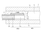
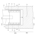
- FIG. 2 is a cross-sectional view parallel to the top wall of the waveguide as viewed from above and below, showing the microstrip line-waveguide converter according to Embodiment 1, located below the top wall of the waveguide.
- 2 is a cross-sectional view taken along line AA shown in FIG. 1 in the microstrip line-waveguide converter according to Embodiment 1.
- FIG. FIG. 2 is a cross-sectional view taken along line BB shown in FIG. 1 in the microstrip line-waveguide converter according to the first embodiment.
- FIG. 2 is a cross-sectional view taken along line CC shown in FIG. 1 in the microstrip line-waveguide converter according to the first embodiment.
- FIG. 7 is a cross-sectional view parallel to the top wall of the waveguide as seen from above and below, showing a microstrip line-waveguide converter according to a comparative example, located below the top wall of the waveguide.
- FIG. 6 is a cross-sectional view taken along line AA shown in FIG. 5 in a microstrip line-waveguide converter according to a comparative example.
- FIG. 6 is a cross-sectional view taken along line BB shown in FIG. 5 in a microstrip line-waveguide converter according to a comparative example.
- FIG. 6 is a cross-sectional view taken along line CC shown in FIG. 5 in a microstrip line-waveguide converter according to a comparative example.
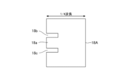
- FIG. 3 is a plan view showing another example of the second ground conductor in the microstrip line-waveguide converter according to Embodiment 1.
- FIG. FIG. 2 is a cross-sectional view corresponding to the BB cross section shown in FIG. 1 in the microstrip line-waveguide converter according to the second embodiment.
- FIG. 7 is a cross-sectional view parallel to the top wall of the waveguide as viewed from above and below, showing the microstrip line-waveguide converter according to Embodiment 3, located below the top wall of the waveguide.
- 12 is a cross-sectional view taken along line AA shown in FIG. 11 in the microstrip line-waveguide converter according to Embodiment 3.
- FIG. 12 is a cross-sectional view taken along line BB shown in FIG.
- FIG. 12 is a cross-sectional view taken along line CC shown in FIG. 11 in the microstrip line-waveguide converter according to Embodiment 3.
- FIG. 12 is a cross-sectional view corresponding to the BB cross section shown in FIG. 11 in the microstrip line-waveguide converter according to Embodiment 5.
- FIG. 12 is a cross-sectional view corresponding to the BB cross section shown in FIG. 11 in the microstrip line-waveguide converter according to the sixth embodiment.
- FIG. 7 is a cross-sectional view of the microstrip line-waveguide converter according to the seventh embodiment, looking downward from the cross section of the third ground conductor.
- 12 is a cross-sectional view taken along line AA shown in FIG. 11 in the microstrip line-waveguide converter according to Embodiment 7.
- FIG. 12 is a cross-sectional view taken along line BB shown in FIG. 11 in the microstrip line-waveguide converter according to Embodiment 7.
- FIG. 12 is a cross-sectional view taken along line CC shown in FIG. 11 in the microstrip line-waveguide converter according to Embodiment 7.
- 20 is a cross-sectional view corresponding to the BB cross section shown in FIG. 19 in the microstrip line-waveguide converter according to the eighth embodiment. 20 is a cross-sectional view corresponding to the BB cross section shown in FIG. 19 in the microstrip line-waveguide converter according to the ninth embodiment.
- Embodiment 1 A microstrip line-waveguide converter according to Embodiment 1 will be explained using FIGS. 1 to 4.
- the microstrip line-waveguide converter according to the first embodiment is a millimeter-wave converter on a flat substrate (hereinafter referred to as a microstrip substrate) on which various high-frequency circuits for signal processing and their peripheral circuits are mounted.
- a high-frequency signal from a microstrip line, which serves as a transmission line for high-frequency signals in a high-frequency region such as a microwave band or a microwave band, is transmitted to a waveguide that does not increase loss during signal transmission.
- microstrip line-waveguide converter that converts a microstrip line to a waveguide will be explained, but conversely, a microstrip line-waveguide converter that converts a waveguide to a microstrip line will be described. It can also be applied to tube converters.
- the microstrip line-waveguide converter according to Embodiment 1 includes one end of a waveguide (hereinafter referred to as waveguide 1) and a converter formed at one end of a microstrip substrate. .
- the waveguide 1 has an upper wall 1a, a lower wall 1b, a right side wall 1c, and a left side wall 1d, and has a transducer forming area at one end.
- the waveguide 1 propagates electromagnetic waves, which are high-frequency signals converted by the microstrip line-waveguide converter, in an electromagnetic wave propagation region communicating from the transducer formation region.
- the waveguide 1 has a rectangular cross section, and the width of the right side wall 1c and the left side wall 1d is shorter than the width of the upper wall 1a and the lower wall 1b.
- the upper, lower, left, and right of the upper wall 1a, the lower wall 1b, the right side wall 1c, and the left side wall 1d are added for convenience of explanation, and the upper wall 1a and the lower wall 1b are a pair of side walls, and the right side wall 1c and the left side wall 1d. may be the upper wall and the lower wall.
- the width of the pair of side walls is narrower than the width of the upper wall and the lower wall.
- the conversion section formed at one end of the microstrip substrate includes a dielectric 11, a first ground conductor 12, a plurality of right through conductors 13, a right ground conductor pad 14, a plurality of left through conductors 15, It includes a left ground conductor pad 16, a signal conductor 17, and a second ground conductor 18.
- the height of the conversion section is shorter than the distance from the inner surface of the lower wall 1b to the inner surface of the upper wall 1a in the waveguide 1.
- the dielectric 11 is a dielectric formed continuously with the dielectric of the microstrip substrate.
- the dielectric 11 is arranged at one end of the waveguide 1, that is, in the transducer formation region, and is fixed to the inner surface of the one end of the lower wall 1b of the waveguide 1 via the first ground conductor 12.
- the dielectric 11 has a cutout 11a that communicates with the waveguide 1 at one end thereof, and has a right side 11b and a left side 11c on each side of the cutout 11a.
- the cutout portion 11a penetrates from the front surface to the back surface of the dielectric 11, and the front surface, the back surface, and the end surface communicating with the waveguide 1 are exposed surfaces.
- the exposed surface on the back side of the notch portion 11a is covered by the lower wall 1b of the waveguide 1.
- the dielectric 11 is, for example, ceramic, which is commonly used in microstrip substrates.
- the first ground conductor 12 is formed on the back surface of the dielectric 11, and one end thereof is electrically and mechanically connected to the inner surface of one end of the lower wall 1b of the waveguide 1 by solder or the like.
- the first ground conductor 12 has a right ground conductor 12a formed on the back surface of the right side 11b of the dielectric 11, and a left ground conductor 12b formed on the back surface of the left side 11c of the dielectric 11.
- the first ground conductor 12 is waveguided parallel to the tube axis of the waveguide 1, specifically, so that the longitudinal direction of the right ground conductor 12a and the left side portion 11c is parallel to the tube axis of the waveguide 1. It is electrically and mechanically connected to the inner surface at one end of the lower wall 1b of the tube 1.
- the first ground conductor 12 is a conductive foil formed continuously with the ground conductor formed on the back surface of the dielectric of the microstrip substrate.
- the plurality of right through conductors 13 each penetrate the right side 11b of the dielectric 11 from the front surface to the back side, are arranged in parallel at equal intervals along the right side 11b, and have their lower ends connected to the right ground conductor of the first ground conductor 12. 12a.
- the plurality of right penetrating conductors 13 are arranged parallel to the tube axis of the waveguide 1 at equal intervals.
- the right ground conductor pad 14 is formed on the surface of the right side 11b of the dielectric 11, is electrically connected to the upper end of the plurality of right through conductors 13, and is connected to the first ground conductor 12 via the plurality of right through conductors 13. is electrically connected to the right ground conductor 12a.
- the longitudinal center axis of the right conductor pad 14 is parallel to the tube axis of the waveguide 1 .
- the electrical connection between the right ground conductor 12a and the right ground conductor pad 14 is preferably made by a plurality of right through conductors 13 arranged at equal intervals parallel to the tube axis of the waveguide 1;
- the right ground conductor 12a and the right ground conductor pad 14 may be electrically connected by the right through conductor 13.
- electrical connection between the right ground conductor 12a and the right ground conductor pad 14 is made by at least one right through conductor 13.
- the plurality of left through conductors 15 each penetrate the left side 11c of the dielectric 11 from the front surface to the back side, are arranged in parallel at equal intervals along the left side 11c, and have their lower ends connected to the left ground conductor 12b of the first ground conductor 12. electrically connected to.
- the plurality of left penetrating conductors 15 are arranged parallel to the tube axis of the waveguide 1 at equal intervals.
- the left ground conductor pad 16 is formed on the surface of the left side 11 c of the dielectric 11 , is electrically connected to the upper ends of the plurality of left through conductors 15 , and is connected to the first ground conductor 12 via the plurality of left through conductors 15 . is electrically connected to the left ground conductor 12b.
- the longitudinal central axis of the left conductor pad 16 is parallel to the tube axis of the waveguide 1 .
- the electrical connection between the left ground conductor 12b and the left ground conductor pad 16 is preferably made by a plurality of left through conductors 15 arranged at equal intervals parallel to the tube axis of the waveguide 1;
- the left ground conductor 12b and the left ground conductor pad 16 may be electrically connected by the left through conductor 15.
- the electrical connection between the left ground conductor 12b and the left ground conductor pad 16 is made by at least one left through conductor 15.
- the plurality of right through conductors 13 and the plurality of left through conductors 15 are formed, for example, in the same manner as a generally known method of forming vias (VIA) in a dielectric material constituting a substrate.
- the right ground conductor pad 14 and the left ground conductor pad 16 are formed, for example, in the same manner as a generally known method of forming a conductive foil on a dielectric material constituting a substrate.
- the signal conductor 17 is formed on the surface of the dielectric 11, and one end reaches a notch 11a formed in the dielectric 11.
- the signal conductor 17 is a line parallel to the tube axis of the waveguide 1.
- the signal conductor 17 is a conductive foil formed continuously with the signal conductor formed on the dielectric surface of the microstrip substrate.
- a signal conductor, a dielectric material, and a ground conductor constitute a microstrip line.
- the signal conductor 17, dielectric 11, and first ground conductor 12 constitute a microstrip line continuous from the microstrip line on the microstrip board.
- the second ground conductor 18 covers the exposed surface of the dielectric 11 on the front side of the notch 11a.
- the back surface of the right side is electrically and mechanically connected to the surface of the right ground conductor pad 14
- the back surface of the left side is electrically and mechanically connected to the surface of the left ground conductor pad 16.
- the back surface of the other end is electrically and mechanically connected to the surface of one end of the signal conductor 17.
- a gap exists between the surface of the second ground conductor 18 and the inner surface of the upper wall 1a of the waveguide 1.
- the length of the second ground conductor 18 in the tube axis direction of the waveguide 1 is 1/4 wavelength of the signal propagating through the waveguide 1 .
- the lower wall 1b, the second ground conductor 18, the right ground conductor 12a, the plurality of right through conductors 13, the right ground conductor pad 14, the left ground conductor 12b, the plurality of left through conductors 15, and the left ground conductor pad 16 constitutes a conversion waveguide WG2 in the conversion section.
- the conversion waveguide WG2 is a hollow waveguide surrounding the notch 11a, and has a relatively high impedance characteristic.
- the other end side of the waveguide 1 from the end face communicating with the waveguide 1 in the notch portion 11a constitutes a propagation waveguide WG1. It is necessary to impedance match the conversion waveguide WG2 and the propagation waveguide WG1, and since the conversion waveguide WG2 is a waveguide with relatively high impedance characteristics, the propagation waveguide WG1 It can also be made into a waveguide with relatively high impedance characteristics.
- Both the conversion waveguide WG2 and the propagation waveguide WG1 are waveguides with high impedance characteristics by making the minimum interval so that they do not electrically short-circuit (in other words, maintain an open state). Therefore, impedance matching between the propagation waveguide WG1 and the conversion waveguide WG2 becomes good.
- the distance from the inner surface of the lower wall 1b of the waveguide 1 to the inner surface of the upper wall 1a of the waveguide 1 can be made the same in the conversion waveguide WG2 and the propagation waveguide WG1, There is no need to make any special modifications to the waveguide 1. Note that the wavelength of the high frequency signal propagating through the conversion waveguide WG2 and the wavelength of the high frequency signal propagating through the propagation waveguide WG1 are the same.
- the conversion waveguide WG2 is electrically connected to the microstrip line on the microstrip board by having the other end of the second ground conductor 18 electrically connected to the signal conductor 17. .
- the length in the tube axis direction of the waveguide 1 in the second ground conductor 18 is 1/4 wavelength of the signal propagating through the waveguide 1, one end of the second ground conductor 18 and the waveguide
- the upper wall 1a of the waveguide 1 is electrically short-circuited to the signal propagating through the waveguide 1 (section X in FIGS. 2 and 3). That is, the conversion waveguide WG2 is electrically connected to the propagation waveguide WG1 at one end for a signal propagating through the waveguide 1.
- the conversion waveguide WG2 in the conversion section transmits the high frequency signal transmitted through the microstrip line in the microstrip board at the location where the signal conductor 17 and the second ground conductor 18 are electrically connected, that is, at the connection section.
- the waveguide 1 is converted into a high frequency signal that propagates, and the converted high frequency signal is propagated to the propagation waveguide WG1 in the waveguide 1. Note that since a gap exists between the other end of the second ground conductor 18 and the upper wall 1a of the waveguide 1, there is a gap between the other end of the second ground conductor 18 and the upper wall 1a of the waveguide 1.
- 1a is an electrically open state (section Y shown in FIGS. 2 and 3).
- One end of the dielectric constituting the microstrip substrate is used as a transducer forming region for forming a microstrip line-waveguide converter.
- the dielectric in the transducer forming region is the dielectric 11 in the microstrip line-waveguide converter.
- a notch 11a is formed in the dielectric 11.
- a first ground conductor 12 is formed on the back surface of the dielectric 11 at the same time as the ground conductor on the microstrip substrate.
- a plurality of right through conductors 13 and a plurality of left through conductors 15 are formed simultaneously with vias (VIAs) which are through conductors in the microstrip substrate.
- VIPs vias
- a right ground conductor pad 14, a left ground conductor pad 16, and a signal conductor 17 are arranged on the surface of a dielectric material constituting a microstrip board as wiring layers and microstrip lines for various high frequency circuits for signal processing and their peripheral circuits. Formed at the same time as the signal conductor constituting the
- the conductor 17 can be formed in the process of forming the microstrip substrate.
- the second ground conductor 18 is placed to cover the exposed surface of the front side of the notch 11a in the dielectric 11, so that the back surface of the right side is the surface of the right ground conductor pad 14, and the back surface of the left side is the left ground conductor.
- the front surface of the pad 16 and the back surface of the other end are electrically and mechanically connected to the surface of one end of the signal conductor 17.
- a microstrip line-waveguide converter can be formed at one end of the microstrip substrate, and the signal conductor 17 in the microstrip line-waveguide converter constitutes a microstrip line in the microstrip substrate. Formed continuously with the signal conductor.
- a microstrip line-waveguide converter formed at one end of the microstrip substrate is inserted into one end of the waveguide 1, and one end of the first ground conductor 12 is connected to the bottom wall 1b of the waveguide 1. Connect electrically and mechanically to the inner surface of one end using solder or the like. Thereby, the microstrip line-waveguide converter is attached to one end of the waveguide 1. Furthermore, a conversion waveguide WG2 which is a hollow waveguide surrounding the notch 11a is formed, and one end of the second ground conductor 18 is connected to the upper wall 1a of the waveguide 1 for signals propagating through the waveguide 1. There will be an electrical short circuit.
- the microstrip line-waveguide converter is connected to the waveguide 1 in a state in which a high frequency signal can be propagated.
- the microstrip line-waveguide converter and the waveguide 1 can be connected, and assembly is easy.
- the gap absorbs the combined dimensional error, for example ⁇ 50 ⁇ m, so the microstrip line-waveguide converter is When attached to the waveguide 1, no stress is applied to the second ground conductor 18 and the upper wall 1a of the waveguide 1.
- the microstrip line-waveguide converter, the microstrip substrate, and the waveguide 1 are not damaged. Furthermore, since the height of the waveguide 1 can be increased, the ratio of dimensional error to the height of the waveguide 1 is small, and the change in electrical characteristics as a microstrip line-waveguide converter is small.
- the high frequency signal transmitted through the microstrip line on the microstrip substrate is transmitted to the microstrip line including the signal conductor 17 in the microstrip line-waveguide converter.
- the high frequency signal transmitted to the microstrip line including the signal conductor 17 is converted to surround the notch 11a at the point where one end of the signal conductor 17 and the other end of the second ground conductor 18 are electrically connected.
- waveguide WG2. The converted high-frequency signal propagates through the conversion waveguide WG2.
- the high frequency signal (electromagnetic wave) propagated through the conversion waveguide WG2 is transmitted through the waveguide 1 from one end of the second ground conductor 18, which is electrically short-circuited to the signal propagated through the waveguide 1. It propagates to the waveguide WG1.
- a gap exists between the surface of the second ground conductor 18 and the inner surface of the upper wall 1a of the waveguide 1, and the second ground conductor Since the length of the waveguide 1 in the tube axis direction at 18 is 1/4 wavelength of the signal propagating through the waveguide 1, one end of the second ground conductor 18 is guided to the upper wall 1a of the waveguide 1.
- the current flowing through the second ground conductor 18 due to the high frequency signal transmitted to the microstrip line including the signal conductor 17 which is electrically short-circuited with respect to the signal propagating through the wave tube 1 is connected to one end of the second ground conductor 18.
- the high frequency signal flows from the waveguide 1 to the upper wall 1a of the waveguide 1, and is propagated to the propagation waveguide WG1 of the waveguide 1.
- the high frequency signal propagating through the conversion waveguide WG2 constituted by the second ground conductor 18 etc. is transmitted from the air gap between the surface of the second ground conductor 18 and the inner surface of the upper wall 1a of the waveguide 1. Will not leak.
- the high frequency signal propagating through the conversion waveguide WG2 is propagated with low loss and is propagated to the propagation waveguide WG1 of the waveguide 1.
- the advantages of providing the conversion waveguide WG2 surrounding the cutout portion 11a will be described below.
- the conversion waveguide WG2 in the first embodiment does not have the notch 11a, that is, the dielectric 11 remains.
- An example using a conversion waveguide WG3 which is a resin waveguide will be shown.
- the conversion waveguide WG3 includes a first ground conductor 12, a second ground conductor 18, a plurality of right through conductors 13, a right ground conductor pad 14, a plurality of left through conductors 15, and a left ground conductor pad 16. Ru.
- the conversion waveguide WG3 is a resin waveguide that surrounds the material of the dielectric 11, and has a relative dielectric constant larger than that of the hollow 1, and furthermore, since the thickness of the dielectric 11 is generally thin, the impedance is low. It becomes a waveguide with extremely low impedance characteristics.
- the distance H2 in the propagation waveguide WG1 is shorter than the thickness of the dielectric 11.
- the distance H2 in the propagation waveguide WG1 is very small, and the height of the waveguide 1 is also inevitably low.
- the microstrip line-waveguide converter according to Embodiment 1 from the inner surface of the waveguide 1 to the lower wall 1b of the waveguide 1 in the conversion waveguide WG2 to the inner surface of the upper wall 1a of the waveguide 1.
- the distance from the inner surface to the lower wall 1b of the waveguide 1 in the propagation waveguide WG1 to the inner surface of the upper wall 1a of the waveguide 1 can be made the same, and the dimensional error with respect to the height of the waveguide 1 can be made the same.
- the change in electrical characteristics of the microstrip line-waveguide converter due to dimensional errors is small.
- the microstrip line-waveguide converter according to the first embodiment can reduce changes in electrical characteristics due to dimensional errors in the height direction from the inner surface of the lower wall 1b of the waveguide 1.
- the microstrip line-waveguide converter has the notch 11a at one end of the dielectric 11, and the lower wall 1b of the waveguide 1 and the second A hollow conductor that surrounds the notch 11a is formed by the ground conductor 18, the right ground conductor 12a, the plural right through conductors 13, the right ground conductor pad 14, the left ground conductor 12b, the plural left through conductors 15, and the left ground conductor pad 16.
- One end of the first ground conductor 12 formed on the back surface of the dielectric 11 constitutes the conversion waveguide WG2, which is a wave tube, and electrically and mechanically connects to the inner surface of one end of the lower wall 1b of the waveguide.
- the microstrip line-waveguide converter is attached to the waveguide 1 by connecting the microstrip line to the waveguide 1, and the other end of the second ground conductor 18 is electrically connected to one end of the signal conductor 17.
- the microstrip line-waveguide converter and the microstrip line on the microstrip board are connected, and the length of the second ground conductor 18 in the tube axis direction of the waveguide 1 propagates through the waveguide 1. Since the microstrip line-waveguide converter and waveguide 1 are connected as a quarter wavelength of the signal, the microstrip line and waveguide 1 on the microstrip substrate of the microstrip line-waveguide converter are connected. Easy to assemble.
- the microstrip line-waveguide converter according to the first embodiment has a gap between the surface of the second ground conductor 18 and the inner surface of the upper wall 1a of the waveguide 1, the dielectric 11 Even if there is a thickness error in the second ground conductor 18, or an error in the distance from the lower wall 1b to the upper wall 1a of the waveguide 1, the air gap absorbs the combined dimensional error, so the micro When attaching the strip line-waveguide converter to the waveguide 1, no stress is applied to the second ground conductor 18 and the upper wall 1a of the waveguide 1, and the microstrip line-waveguide converter and The microstrip substrate and waveguide 1 will not be damaged.
- the microstrip line-waveguide converter according to the first embodiment configures the conversion waveguide WG2 which is a hollow waveguide
- the conversion waveguide WG2 is a high-impedance characteristic guide.
- the propagation waveguide WG1 in the waveguide 1 can be a waveguide with high impedance characteristics, and the height of the waveguide 1 can be increased, so the dimensional error in the height of the waveguide 1 can be reduced. Since the ratio of 1 to 1 is small, changes in the electrical characteristics of the microstrip line-to-waveguide converter due to dimensional errors in the height direction from the inner surface of the lower wall 1b of the waveguide 1 can be reduced.
- the current flowing through the second ground conductor 18 due to the high frequency signal transmitted to the microstrip line including the signal conductor 17 is The high-frequency signal flows from one end of the waveguide 18 to the upper wall 1a of the waveguide 1, and is propagated to the propagation waveguide WG1 of the waveguide 1. Even though a gap is provided between the wall 1a and the inner surface of the wall 1a, the high frequency signal propagating through the conversion waveguide WG2 does not leak from the gap, and the high frequency signal propagating through the conversion waveguide WG2 has a wide band. and propagates with low loss.
- the second ground conductor 18 in the microstrip line-waveguide converter according to the first embodiment is a second ground conductor 18 having slits 18b and 18c parallel to one end of the signal conductor 17, as shown in FIG. It is also possible to use the second ground conductor 18A.
- the second ground conductor 18A shown in FIG. It has slits 18b and 18c.
- the impedance matching from the microstrip line to the conversion waveguide WG2 on the microstrip board can be set better, and the impedance matching can be set better for broadband high-frequency signals. Reflective properties can be obtained.
- the number of slits 18b and 18c is not limited to two, and may be one or three or more. Considering the impedance matching between the microstrip line and the conversion waveguide WG2 on the microstrip board, the number of slits is Just choose the number, location, and dimensions appropriately.
- 1/4 wavelength includes not only 1/4 wavelength but also odd multiples of 1/4 wavelength.
- Embodiment 2 A microstrip line-waveguide converter according to Embodiment 2 will be explained using FIG. 10.
- the microstrip line-waveguide converter according to the second embodiment has a flat inner surface of the upper wall 1a of the waveguide 1 in the microstrip line-waveguide converter according to the first embodiment. The difference is that a step is provided, but the other points are the same. Note that in FIG. 10, the same reference numerals as those shown in FIGS. 1 to 4 indicate the same or corresponding parts.
- the upper wall 1a of the waveguide 1 which is different from the microstrip line-waveguide converter according to the first embodiment, will be mainly described below.
- the distance h2 from the surface of the signal conductor 17 at a position not connected to the second ground conductor 18 to the inner surface 1a2 of the upper wall 1a of the waveguide 1 is It is longer than the distance h1 from the surface of the ground conductor 18 to the inner surface 1a1 of the upper wall 1a of the waveguide 1.
- the entire upper wall 1a from a plane perpendicular to the tube axis of the waveguide 1 including the other end surface of the second ground conductor 18 to one end surface of the waveguide 1.
- the thickness of the upper wall 1a is reduced to provide a step on the upper wall 1a, and the distance h2 is made longer than the distance h1.
- the gap between the microstrip line including the signal conductor 17 and the top wall 1a of the waveguide 1 is longer than the gap between the conversion waveguide WG2 and the top wall 1a of the waveguide 1.
- the air gap between the microstrip line including the signal conductor 17 and the upper wall 1a of the waveguide 1 extends from the surface of the signal conductor 17 constituting the microstrip line to the conversion waveguide WG2, that is, the second It is longer than the distance to the horizontal plane extending from the inner surface 1a1 of the upper wall 1a of the waveguide 1 located on the ground conductor 18.
- connection portion and the upper wall 1a of the waveguide 1 can be opened more reliably with respect to the high-frequency signal propagated to the conversion waveguide WG2.
- one end of the second ground conductor 18 and the upper wall 1a of the waveguide 1 are more reliably electrically short-circuited with respect to the signal propagating in the waveguide 1, and the surface of the second ground conductor 18 is It is possible to further reduce the leakage of the high frequency signal propagated to the conversion waveguide WG2 from the gap between the inner surface of the upper wall 1a of the waveguide 1, and to obtain a microstrip line-waveguide converter with lower loss. .
- the microstrip line-waveguide converter according to the second embodiment has the same effects as the microstrip line-waveguide converter according to the first embodiment, and also has the same effect as the high-frequency wave propagating through the conversion waveguide WG2. Signals can be propagated with lower loss.
- Embodiment 3 A microstrip line-waveguide converter according to Embodiment 3 will be explained using FIGS. 11 to 14.
- the microstrip line-waveguide converter according to the third embodiment has a stub dielectric 19 on the surface of the second ground conductor 18, unlike the microstrip line-waveguide converter according to the first embodiment.
- the difference is that the stub through conductor 20 and the stub conductor 21 are arranged, and the other points are the same.
- FIGS. 11 to 14 the same reference numerals as those shown in FIGS. 1 to 4 indicate the same or corresponding parts.
- the microstrip line-waveguide converter according to the third embodiment like the microstrip line-waveguide converter according to the first embodiment, has a waveguide 1 formed at one end of the microstrip substrate. and a conversion unit.
- the waveguide 1 has an upper wall 1a, a lower wall 1b, a right side wall 1c, and a left side wall 1d, and transmits electromagnetic waves that are high frequency signals.
- the waveguide 1 has a rectangular cross section, and the width of the upper wall 1a and the lower wall 1b is longer than the width of the right side wall 1c and the left side wall 1d.
- the conversion section includes a dielectric 11, a first ground conductor 12, a plurality of right through conductors 13, a right ground conductor pad 14, a plurality of left through conductors 15, a left ground conductor pad 16, and a signal conductor. 17, a second ground conductor 18, a stub dielectric 19, a stub through conductor 20, and a stub conductor 21.
- the height of the conversion section is shorter than the distance from the inner surface of the lower wall 1b to the inner surface of the upper wall 1a in the waveguide 1.
- Reference numeral 18 indicates the dielectric 11, the first ground conductor 12, the plurality of right through conductors 13, the right ground conductor pad 14, and the plurality of left through conductors in the conversion part of the microstrip line-waveguide converter according to the first embodiment.
- the conductor 15, the left ground conductor pad 16, the signal conductor 17, and the second ground conductor 18 are the same or substantially the same.
- the dielectric 11 is a dielectric formed continuously with the dielectric of the microstrip substrate, and is disposed at the end of the waveguide 1, and has a notch 11a communicating with the waveguide 1 at one end.
- the cutout portion 11a has a right side portion 11b and a left side portion 11c on each side of the cutout portion 11a.
- the first ground conductor 12 is formed on the back surface of the dielectric 11, and one end thereof is electrically and mechanically connected to the inner surface of one end of the lower wall 1b of the waveguide 1.
- the first ground conductor 12 has a right ground conductor 12a formed on the back surface of the right side 11b of the dielectric 11, and a left ground conductor 12b formed on the back surface of the left side 11c of the dielectric 11.
- the first ground conductor 12 is a conductive foil formed continuously with the ground conductor formed on the back surface of the dielectric of the microstrip substrate.
- the plurality of right through conductors 13 each penetrate the right side 11b of the dielectric 11 from the front surface to the back side, are arranged in parallel at equal intervals along the right side 11b, and have their lower ends connected to the right ground conductor of the first ground conductor 12. 12a.
- the right ground conductor pad 14 is formed on the surface of the right side 11b of the dielectric 11, is electrically connected to the upper end of the plurality of right through conductors 13, and is connected to the first ground conductor 12 via the plurality of right through conductors 13. is electrically connected to the right ground conductor 12a.
- the plurality of left through conductors 15 each penetrate the left side 11c of the dielectric 11 from the front surface to the back side, are arranged in parallel at equal intervals along the left side 11c, and have their lower ends connected to the left ground conductor 12b of the first ground conductor 12. electrically connected to.
- the left ground conductor pad 16 is formed on the surface of the left side 11 c of the dielectric 11 , is electrically connected to the upper ends of the plurality of left through conductors 15 , and is connected to the first ground conductor 12 via the plurality of left through conductors 15 . is electrically connected to the left ground conductor 12b.
- the signal conductor 17 is formed on the surface of the dielectric 11, and one end reaches a notch 11a formed in the dielectric 11.
- the signal conductor 17 is a line parallel to the tube axis of the waveguide 1.
- the signal conductor 17 is a conductive foil formed continuously with the signal conductor formed on the dielectric surface of the microstrip substrate.
- the signal conductor 17, the dielectric 11, and the first ground conductor 12 constitute a microstrip line continuous from the microstrip line on the microstrip board.
- the second ground conductor 18 covers the exposed surface of the dielectric 11 on the front side of the notch 11a.
- the back surface of the right side is electrically and mechanically connected to the surface of the right ground conductor pad 14
- the back surface of the left side is electrically and mechanically connected to the surface of the left ground conductor pad 16.
- the back surface of the other end is electrically and mechanically connected to the surface of one end of the signal conductor 17.
- the lower wall 1b, the second ground conductor 18, the right ground conductor 12a, the plurality of right through conductors 13, the right ground conductor pad 14, the left ground conductor 12b, the plurality of left through conductors 15, and the left ground conductor pad 16 constitutes a conversion waveguide WG2 in the conversion section.
- the conversion waveguide WG2 is a hollow waveguide surrounding the notch 11a, and has a relatively high impedance characteristic. Since the conversion waveguide WG2 has a relatively high impedance characteristic, the propagation waveguide WG1 in the waveguide 1 can also easily obtain a relatively high high impedance characteristic, and the propagation waveguide WG1 and the conversion waveguide It is easy to match the impedance of tube WG2.
- the back surface of the stub dielectric 19 is joined to the surface of the second ground conductor 18 .
- the stub dielectric 19 is, for example, ceramic like the dielectric 11.
- the length of the waveguide 1 in the tube axis direction and the width perpendicular to the tube axis direction in the stub dielectric 19 are the same as the length in the tube axis direction of the waveguide 1 in the second ground conductor 18 and the width in the tube axis direction of the waveguide 1 in the second ground conductor 18. It is the same as the length of the width perpendicular to the axial direction.
- the size of the stub dielectric 19 does not necessarily have to be the same as the size of the second ground conductor 18, and may be slightly smaller.
- the stub through conductor 20 is located at the center in the width direction of one end of the stub dielectric 19, penetrates from the front surface to the back surface of the stub dielectric 19, and has a lower end electrically connected to the second ground conductor 18. Ru.
- the stub through conductor 20 is formed, for example, in the same manner as a generally known method of forming vias (VIA) in a dielectric material constituting a multilayer wiring board.
- the back surface of the stub conductor 21 is joined to the surface of the stub dielectric 19.
- the stub conductor 21 is electrically connected to the second ground conductor 18 on the back surface of one end by the stub penetrating conductor 20 .
- a gap exists between the surface of the stub conductor 21 and the inner surface of the upper wall 1a of the waveguide 1.
- the length in the tube axis direction of the waveguide 1 in the stub conductor 21 is the length from the connection part 20a between the lower end of the stub penetrating conductor 20 and the surface of the second ground conductor 18 to the other end of the stub conductor 21.
- the wavelength is determined to be 1/4 wavelength of the signal propagating through the waveguide 1.
- connection part 20a between the lower end of the stub through conductor 20 and the surface of the second ground conductor 18, the stub through conductor 20, and the upper end of the stub through conductor 20 and one end of the back surface of the stub conductor 21.
- the length from the connecting portion 20b to the other end of the stub conductor 21 is 1/4 wavelength of the signal propagating through the waveguide 1. Therefore, the stub dielectric 19, the stub through conductor 20, the stub conductor 21, and the second ground conductor 18 operate as a 1/4 wavelength stub with an open end in the conversion section.
- the other end of the stub conductor 21 and the upper wall 1a of the waveguide 1 are electrically It is in an open state (section Y shown in FIG. 13).
- the length from the connection part 20a between the lower end of the stub through conductor 20 and the surface of the second ground conductor 18 to the other end of the stub conductor 21 is 1/4 wavelength of the signal propagating through the waveguide 1. Therefore, the stub conductor 21 and the second ground conductor 18 operate as a 1/4 wavelength stub with an open end.
- the second ground conductor 18 and the stub conductor 21 operate as a 1/4 wavelength stub, one end of the second ground conductor 18 is connected to the upper wall 1a of the waveguide 1. This results in an electrical short circuit (section X in FIG. 13) for the signal propagating through.
- the conversion waveguide WG2 is electrically connected to the microstrip line on the microstrip substrate by electrically connecting the second ground conductor 18 to the signal conductor 17 at the other end.
- the conversion waveguide WG2 at one end of the conversion waveguide WG2, one end of the second ground conductor 18 and the upper wall 1a of the waveguide 1 are electrically short-circuited with respect to the signal propagating through the waveguide 1.
- it is electrically connected to the propagation waveguide WG1.
- the stub dielectric 19 is arranged in alignment with the second ground conductor 18 such that the back surface of the stub dielectric 19 is joined to the front surface of the second ground conductor 18 .
- a through conductor 20 for stub is formed.
- the stub dielectric 19 and the stub through conductor 20 are formed by a generally known method for forming a dielectric and a via (VIA) in a multilayer wiring board.
- the stub conductor 21 is formed on the surface of the stub dielectric 19 so as to be electrically connected to the upper end of the stub through conductor 20 .
- the stub conductor 21 is formed on the surface of the stub dielectric 19, for example, in the same manner as the generally known method of forming a conductor foil on a dielectric that constitutes a substrate.
- a microstrip line-to-waveguide converter having an open-ended 1/4 wavelength stub can be formed at one end of the microstrip substrate, and the signal conductor 17 in the microstrip line-to-waveguide converter can be formed at one end of the microstrip substrate. It is formed continuously with the signal conductor constituting the microstrip line on the microstrip board.
- a microstrip line-waveguide converter formed at one end of the microstrip substrate is inserted into one end of the waveguide 1, and one end of the first ground conductor 12 is connected to the bottom wall 1b of the waveguide 1. Connect electrically and mechanically to the inner surface of one end using solder or the like. Thereby, the microstrip line-waveguide converter is attached to one end of the waveguide 1. Furthermore, a conversion waveguide WG2, which is a hollow waveguide surrounding the notch 11a, is formed, and the stub conductor 21 and the second ground conductor 18 operate as a 1/4 wavelength stub with an open end. One end of the second ground conductor 18 and the upper wall 1a of the waveguide 1 are electrically short-circuited with respect to a signal propagating through the waveguide 1.
- the microstrip line-waveguide converter is connected to the waveguide 1 in a state in which a high frequency signal can be propagated.
- the microstrip line-waveguide converter is connected.
- the waveguide 1 can be connected and assembly is easy.
- the air gap absorbs the combined dimensional error, making it easy to guide the microstrip line-waveguide converter.
- the microstrip line-waveguide converter, the microstrip substrate, and the waveguide 1 are not damaged.
- the high frequency signal transmitted through the microstrip line on the microstrip substrate is transmitted to the microstrip line including the signal conductor 17 in the microstrip line-waveguide converter.
- the high frequency signal transmitted to the microstrip line including the signal conductor 17 is converted to surround the notch 11a at the point where one end of the signal conductor 17 and the other end of the second ground conductor 18 are electrically connected.
- waveguide WG2. The converted high-frequency signal propagates through the conversion waveguide WG2.
- the high frequency signal (electromagnetic wave) propagated through the conversion waveguide WG2 is guided from one end of the second ground conductor 18 which is electrically short-circuited to the signal propagated through the waveguide 1 by the stub conductor 21. It propagates to the propagation waveguide WG1 of the tube 1.
- a gap exists between the surface of the stub conductor 21 and the inner surface of the upper wall 1a of the waveguide 1, and the stub conductor 21 and the second Since the ground conductor 18 operates as a 1/4 wavelength stub with an open end, one end of the second ground conductor 18 is electrically connected to the upper wall 1a of the waveguide 1 for signals propagating through the waveguide 1.
- the current flowing through the second ground conductor 18 due to the short-circuited high-frequency signal transmitted to the microstrip line including the signal conductor 17 flows from one end of the second ground conductor 18 to the upper wall 1a of the waveguide 1, and the high-frequency The signal is propagated to the propagation waveguide WG1 of the waveguide 1.
- the high frequency signal propagating through the conversion waveguide WG2 constituted by the second ground conductor 18 etc. will not leak from the gap between the surface of the stub conductor 21 and the inner surface of the upper wall 1a of the waveguide 1. There is no.
- the high frequency signal propagating through the conversion waveguide WG2 is propagated with low loss and is propagated to the propagation waveguide WG1 of the waveguide 1.
- the microstrip line-waveguide converter according to the third embodiment is similar to the microstrip line-waveguide converter according to the first embodiment.
- the conversion waveguide WG2 which is a wave tube, is configured such that one end of the first ground conductor 12 formed on the back surface of the dielectric 11 is electrically and mechanically connected to the inner surface at one end of the lower wall 1b of the waveguide.
- the microstrip line-waveguide converter is attached to the waveguide 1 by connecting the microstrip line to the waveguide 1, and the other end of the second ground conductor 18 is electrically connected to one end of the signal conductor 17.
- the microstrip line-waveguide converter and the microstrip line on the microstrip board are connected, and the stub conductor 21, which operates as an open-ended 1/4 wavelength stub, and the second ground conductor 18 are connected to the second ground conductor 18. Since it is arranged on the surface of the ground conductor 18, it is easy to assemble the microstrip line-waveguide converter to the microstrip line and waveguide 1 on the microstrip substrate.
- the microstrip line-waveguide converter according to the third embodiment has a gap between the surface of the stub conductor 21 and the inner surface of the upper wall 1a of the waveguide 1, the thickness of the dielectric 11 can be reduced. Even if there is an error, a thickness error of the second ground conductor 18, an error in the distance from the lower wall 1b to the upper wall 1a of the waveguide 1, or a thickness error in the stub dielectric 19, the combined dimensional error When the microstrip line-waveguide converter is attached to the waveguide 1, the air gap absorbs the No stress is applied and the microstrip line-waveguide converter, microstrip substrate, and waveguide 1 are not damaged.
- the microstrip line-waveguide converter according to the third embodiment configures the conversion waveguide WG2 which is a hollow waveguide
- the conversion waveguide WG2 is a guide with high impedance characteristics.
- the propagation waveguide WG1 in the waveguide 1 can be a waveguide with high impedance characteristics, and the height of the waveguide 1 can be increased, so the dimensional error in the height of the waveguide 1 can be reduced. Since the ratio of 1 to 1 is small, changes in the electrical characteristics of the microstrip line-to-waveguide converter due to dimensional errors in the height direction from the inner surface of the lower wall 1b of the waveguide 1 can be reduced.
- the current flowing through the second ground conductor 18 due to the high frequency signal transmitted to the microstrip line including the signal conductor 17 is Since the conductor 18 and the stub conductor 21 operate as a 1/4 wavelength stub with an open end, a high-frequency signal flows from one end of the second ground conductor 18 to the upper wall 1a of the waveguide 1, and the high-frequency signal propagates through the waveguide 1. Even though a gap is provided between the surface of the stub conductor 21 and the inner surface of the upper wall 1a of the waveguide 1, the signal propagates through the conversion waveguide WG2. The high frequency signal does not leak from the gap, and the high frequency signal propagating through the conversion waveguide WG2 propagates in a wide band and with low loss.
- the second ground conductor 18 in the microstrip line-waveguide converter according to the third embodiment is a second ground conductor 18 having slits 18b and 18c parallel to one end of the signal conductor 17, as shown in FIG. It is also possible to use the second ground conductor 18A.
- a second ground conductor 18A shown in FIG. 15 is provided on each side of the signal conductor connecting portion 18a that is electrically and mechanically connected to the surface of one end of the signal conductor 17 in parallel with the signal conductor connecting portion 18a. It has slits 18b and 18c.
- the impedance matching from the microstrip line to the conversion waveguide WG2 on the microstrip board can be set better, and the impedance matching can be set better for broadband high-frequency signals. Reflective properties can be obtained.
- the number of slits 18b and 18c is not limited to two, and may be one or three or more. Considering the impedance matching between the microstrip line and the conversion waveguide WG2 on the microstrip board, the number of slits 18b and 18c is not limited to two. Just choose the number, location, and dimensions appropriately.
- Embodiment 4 A microstrip line-waveguide converter according to Embodiment 4 will be explained using FIG. 16.
- the microstrip line-waveguide converter according to the fourth embodiment has a flat inner surface of the upper wall 1a of the waveguide 1 in the microstrip line-waveguide converter according to the third embodiment. The difference is that a step is provided, but the other points are the same.
- FIG. 16 the same reference numerals as those shown in FIGS. 11 to 14 indicate the same or equivalent parts.
- the upper wall 1a of the waveguide 1 which is different from the microstrip line-waveguide converter according to the third embodiment, will be mainly explained below.
- the distance h4 from the surface of the signal conductor 17 at a position not connected to the second ground conductor 18 to the inner surface 1a2 of the upper wall 1a of the waveguide 1 is equal to It is longer than the distance h3 from the surface of 21 to the inner surface 1a1 of the upper wall 1a of the waveguide 1.
- the upper wall 1a is made thinner, a step is provided on the upper wall 1a, and the distance h4 is made longer than the distance h3.
- the gap between the microstrip line including the signal conductor 17 and the top wall 1a of the waveguide 1 is longer than the gap between the conversion waveguide WG2 and the top wall 1a of the waveguide 1.
- the air gap between the microstrip line including the signal conductor 17 and the upper wall 1a of the waveguide 1 extends from the surface of the signal conductor 17 constituting the microstrip line to the conversion waveguide WG2, that is, the stub conductor. It is longer than the distance to the horizontal plane extending from the inner surface 1a1 of the upper wall 1a of the waveguide 1 located on the waveguide 21.
- the distance from the surface of the signal conductor 17 at a position not connected to the second ground conductor 18 to the inner surface of the upper wall 1a of the waveguide 1 is equal to the distance from the surface of the signal conductor 17 to the stub conductor 21.
- an open-ended 1/4 wavelength stub is formed by the stub conductor 21 and the second ground conductor 18. , the open end becomes more open, and one end of the second ground conductor 18, that is, the waveguide side, is more short-circuited to the upper wall 1a of the waveguide 1 with respect to the signal propagating in the waveguide 1. (short circuit), the leakage of high-frequency signals from the gap between the conversion waveguide WG2 and the upper wall 1a of the waveguide 1 can be further reduced, and a microstrip line-waveguide converter with lower loss can be achieved. can get.
- the microstrip line-waveguide converter according to the fourth embodiment has the same effect as the microstrip line-waveguide converter according to the third embodiment, and also has the same effect as the microstrip line-waveguide converter according to the third embodiment. Signals can be propagated with lower loss.
- the second ground conductor 18 is As shown in FIG. 15, the second ground conductor 18A may have slits 18b and 18c parallel to one end of the signal conductor 17.
- Embodiment 5 A microstrip line-waveguide converter according to Embodiment 5 will be explained using FIG. 17.
- the microstrip line-waveguide converter according to the fifth embodiment has a flat inner surface of the upper wall 1a of the waveguide 1 in the microstrip line-waveguide converter according to the third embodiment. The difference is that a step is provided, but the other points are the same. Note that in FIG. 17, the same reference numerals as those shown in FIGS. 11 to 14 indicate the same or equivalent parts.
- the inner surface 1a3 of the upper wall 1a of the waveguide 1 constituting the propagation waveguide WG1 is similar to the inner surface 1a3 of the upper wall 1a of the waveguide 1 where the conversion waveguide WG2 is located.
- the distance h5 from the inner surface of the lower wall 1b of the waveguide 1 constituting the propagation waveguide WG1 to the inner surface 1a3 of the upper wall 1a is below the waveguide 1 where the conversion waveguide WG2 is located. It is shorter than the distance h6 from the inner surface of the wall 1b to the inner surface 1a4 of the upper wall 1a.
- the dielectric 11 is arranged from a plane perpendicular to the tube axis of the waveguide 1 including one end surface of the dielectric 1 to one end surface of the waveguide 1.
- the entire thickness of the upper wall 1a is reduced at the position where the upper wall 1a is located, a step is provided on the upper wall 1a, and the distance h5 is made shorter than the distance h6.
- from the inner surface of the lower wall 1b of the waveguide 1 constituting the propagation waveguide WG1, that is, the lower wall 1b to which the first ground conductor 12 is not connected to the inner surface 1a3 of the upper wall 1a of the waveguide 1.
- the distance from the inner surface of the lower wall 1b of the waveguide 1 where the conversion waveguide WG2 is located to the surface of the second ground conductor 18 is made approximately the same.
- the gap between the surface of the stub conductor 21 and the inner surface 1a4 of the upper wall 1a of the waveguide 1 is narrowed, and the open end formed by the stub conductor 21 and the second ground conductor 18 is By shortening the distance between the 1/4 wavelength stub and the inner surface 1a3 of the upper wall 1a of the waveguide 1, one end of the second ground conductor 18 and the top of the waveguide 1 are connected to the signal propagating in the waveguide 1.
- a microstrip line-waveguide converter can be obtained.
- the second ground conductor 18 is As shown in FIG. 15, the second ground conductor 18A may have slits 18b and 18c parallel to one end of the signal conductor 17.
- the microstrip line-waveguide converter according to the fourth embodiment is not connected to the second ground conductor 18.
- the distance from the surface of the signal conductor 17 at the position to the inner surface of the upper wall 1a of the waveguide 1 extends from the surface of the signal conductor 17 to the inner surface of the upper wall of the waveguide located on the stub conductor 21. It may be longer than the distance to the horizontal plane.
- Embodiment 6 A microstrip line-waveguide converter according to Embodiment 6 will be explained using FIG. 18.
- the microstrip line-waveguide converter according to the sixth embodiment is different from the microstrip line-waveguide converter according to the third embodiment in that the stub conductor 21 and the second ground conductor 18 have an open end. Although a four-wavelength stub is configured, the stub conductor 21 and the second ground conductor 18 are configured to resonate within the stub dielectric 19 with respect to the frequency of the signal propagating through the waveguide 1. They are different and are otherwise the same. Note that in FIG. 18, the same reference numerals as those shown in FIGS. 11 to 14 indicate the same or equivalent parts.
- the dielectric for the stub will be explained with respect to the frequency of the signal propagating in the waveguide 1 using the stub conductor 21 and the second ground conductor 18, which are different from the microstrip line-waveguide converter according to the third embodiment.
- the configuration that causes resonance within 19 will be mainly explained.
- the back surface of the stub dielectric 19 is joined to the surface of the second ground conductor 18 .
- the stub dielectric 19 is, for example, ceramic like the dielectric 11.
- the length of the waveguide 1 in the tube axis direction and the width perpendicular to the tube axis direction in the stub dielectric 19 are the same as the length in the tube axis direction of the waveguide 1 in the second ground conductor 18 and the width in the tube axis direction of the waveguide 1 in the second ground conductor 18.
- the length of the width perpendicular to the axial direction is the same.
- the size of the stub dielectric 19 does not necessarily have to be the same as the size of the second ground conductor 18, and may be slightly smaller.
- the stub through conductor 20 is located at the center in the width direction of one end of the stub dielectric 19, penetrates from the front surface to the back surface of the stub dielectric 19, and has a lower end electrically connected to the second ground conductor 18. Ru.
- the stub through conductor 20 is formed, for example, in the same manner as a generally known method of forming a via (VIA) in a dielectric material constituting a multilayer wiring board.
- the back surface of the stub conductor 21 is joined to the surface of the stub dielectric 19.
- the stub conductor 21 is electrically connected to the second ground conductor 18 on the back surface of one end by the stub penetrating conductor 20 .
- a gap exists between the surface of the stub conductor 21 and the inner surface of the upper wall 1a of the waveguide 1.
- the stub conductor 21 cooperates with the second ground conductor 18 to cause resonance within the stub dielectric 19 with respect to the frequency of the signal propagating through the waveguide 1 . That is, the frequency of the signal propagating through the waveguide 1 resonates within the stub dielectric 19 surrounded by the stub conductor 21, the stub penetrating conductor 20, and the second ground conductor 18.
- the length of the stub conductor 21 in the tube axis direction of the waveguide 1 is determined to be a length at which the frequency of the signal propagating through the waveguide 1 resonates.
- the other end of the stub conductor 21 and the upper wall 1a of the waveguide 1 are electrically It is in an open state (section Y shown in FIG. 18).
- the frequency of the signal propagating through the waveguide 1 resonates within the stub dielectric 19 surrounded by the stub conductor 21, the stub through conductor 20, and the second ground conductor 18, so that as a result, the frequency of the signal propagating through the waveguide 1 resonates.
- One end of the second ground conductor 18 and the upper wall 1a of the waveguide 1 become electrically short-circuited (X section in FIG. 18) with respect to the signal propagating in the waveguide 1.
- the conversion waveguide WG2 is electrically connected to the microstrip line on the microstrip substrate by electrically connecting the second ground conductor 18 to the signal conductor 17 at the other end.
- the conversion waveguide WG2 at one end of the conversion waveguide WG2, one end of the second ground conductor 18 and the upper wall 1a of the waveguide 1 are electrically short-circuited with respect to the signal propagating through the waveguide 1.
- the signal propagating through the waveguide 1 is electrically connected to the propagation waveguide WG1.
- the microstrip line-waveguide converter according to the sixth embodiment is also easily assembled and operates similarly to the microstrip line-waveguide converter according to the third embodiment. and has a similar effect.
- the second ground conductor 18 is As shown in FIG. 15, the second ground conductor 18A may have slits 18b and 18c parallel to one end of the signal conductor 17.
- the microstrip line-waveguide converter is not connected to the second ground conductor 18.
- the distance from the surface of the signal conductor 17 at the position to the inner surface of the upper wall 1a of the waveguide 1 extends from the surface of the signal conductor 17 to the inner surface of the upper wall of the waveguide located on the stub conductor 21. It may be longer than the distance to the horizontal plane.
- the propagation waveguide in the waveguide 1 is The distance from the inner surface of the lower wall 1b of the waveguide 1 constituting WG1 to the inner surface 1a3 of the upper wall 1a is the distance from the inner surface of the lower wall 1b of the waveguide 1 where the conversion waveguide WG2 is located to the upper wall. It may be shorter than the distance to the inner surface 1a4 of 1a.
- Embodiment 7 A microstrip line-waveguide converter according to Embodiment 7 will be explained using FIGS. 19 to 22.
- the microstrip line-waveguide converter according to the seventh embodiment has a stub dielectric 19, a stub through conductor 20, and a stub conductor 21.
- the stub conductor 21 is disposed on the surface of the second ground conductor 18 with a gap between the surface of the stub conductor 21 and the inner surface of the upper wall 1a of the waveguide 1.
- the through conductor 20, the stub conductor 21, and the third ground conductor 22 are attached to the inner surface of the upper wall 1a of the waveguide 1 with a gap between the surface of the stub conductor 21 and the surface of the second ground conductor 18.
- the arrangement is different, and the other points are the same. Note that in FIGS. 19 to 22, the same reference numerals as those used in FIGS. 1 to 4 and FIGS. 11 to 14 indicate the same or equivalent parts.
- reference numeral 16 constitutes a conversion waveguide WG2 in the conversion section, which is a hollow waveguide surrounding the notch 11a.
- the conversion waveguide WG2 is electrically connected to the microstrip line on the microstrip board by electrically connecting the second ground conductor 18 to the signal conductor 17 at the other end.
- the stub dielectric 19, the stub through conductor 20, the stub conductor 21, and the third ground conductor 22 constitute a stub substrate that operates as a quarter-wavelength stub with an open end in the conversion section.
- the stub dielectric 19 is arranged so that its surface faces the surface of the second ground conductor 18 .
- the stub dielectric 19 is, for example, ceramic like the dielectric 11.
- the length of the waveguide 1 in the tube axis direction and the width perpendicular to the tube axis direction in the stub dielectric 19 are the same as the length in the tube axis direction of the waveguide 1 in the second ground conductor 18 and the width in the tube axis direction of the waveguide 1 in the second ground conductor 18. It is the same as the length of the width perpendicular to the axial direction.
- the size of the stub dielectric 19 does not necessarily have to be the same as the size of the second ground conductor 18, and may be slightly smaller.
- the stub dielectric 19 is fixed to the inner surface of one end of the upper wall 1 a of the waveguide 1 via the third ground conductor 22 . That is, the third ground conductor 22 is formed on the back surface of the stub dielectric, and the back surface is electrically and mechanically connected to the inner surface at one end of the upper wall 1a of the waveguide 1 by soldering or the like.
- the stub through conductor 20 is located at the center in the width direction of one end of the stub dielectric 19, penetrates from the front surface to the back surface of the stub dielectric 19, and has a lower end electrically connected to the third ground conductor 22. Ru.
- the stub through conductor 20 is formed, for example, in the same manner as a generally known method of forming a via (VIA) in a dielectric material.
- the stub conductor 21 has its front surface facing the surface of the second ground conductor 18 with a gap in between, and its back surface joined to the surface of the stub dielectric 19 .
- the stub conductor 21 is electrically connected to the third ground conductor 22 on the back surface of one end by the stub penetrating conductor 20 .
- the stub conductor 21 and the third ground conductor 22 are electrically connected by a stub through conductor 20 at the widthwise center of one end of the stub dielectric 19, and
- the length in the axial direction from the connection part 20a between the lower end of the through conductor 20 for stub and the surface of the third ground conductor 22 to the other end of the conductor 21 for stub is the length of the signal propagating through the waveguide 1.
- the wavelength is determined to be 1/4 wavelength.
- connection part 20a between the lower end of the through conductor 20 for stub and the surface of the third ground conductor 22 the through conductor 20 for stub, and the upper end of the through conductor 20 for stub and one end of the back surface of the conductor 21 for stub.
- the length from the connecting portion 20b to the other end of the stub conductor 21 is 1/4 wavelength of the signal propagating through the waveguide 1.
- the other end of the stub conductor 21 and the surface of the second ground conductor 18 are electrically open. state (section Y shown in FIG. 20).
- the length from the connection part 20a between the lower end of the through conductor 20 for stub and the surface of the third ground conductor 22 to the other end of the conductor 21 for stub is 1/4 wavelength of the signal propagating in the waveguide 1. Therefore, the stub conductor 21 and the third ground conductor 22 operate as a 1/4 wavelength stub with an open end. Therefore, one end of the second ground conductor 18 is electrically shorted (Fig. 20 (X section shown).
- one end of the second ground conductor 18 and the upper wall 1a of the waveguide 1 are electrically connected to the signal propagating in the waveguide 1 via the stub substrate. This causes a short circuit and the signal propagating through the waveguide 1 is electrically connected to the propagation waveguide WG1.
- a stub conductor 20 is formed to pass through the stub, and a stub conductor 21, which is a conductor foil, is formed on the surface of the stub dielectric 19 to produce a stub substrate that operates as a 1/4 wavelength stub with an open end.
- the third ground conductor 22, the stub through conductor 20, and the stub conductor 21 are formed on the stub dielectric 19 by a forming method generally known in this field.
- the third ground conductor 22 is electrically and mechanically connected to the set inner surface of the upper wall 1a of the waveguide 1 by soldering or the like, and the stub substrate is connected to the set inner surface of the upper wall 1a of the waveguide 1. It is fixed to one end of the upper wall 1a.
- a microstrip line-waveguide converter formed at one end of the microstrip substrate is inserted into one end of the waveguide 1, and the surface of the second ground conductor 18 is aligned with the third ground conductor 22 on the stub substrate.
- one end of the first ground conductor 12 is electrically and mechanically connected to the inner surface of one end of the lower wall 1b of the waveguide 1 by solder or the like.
- a conversion waveguide WG2 that is a hollow waveguide surrounding the notch 11a is formed, and a microstrip line-waveguide conversion in which a stub substrate is provided for the second ground conductor 18 is formed.
- the device is attached to one end of the waveguide 1.
- the stub substrate which operates as a 1/4 wavelength stub with an open end, allows one end of the second ground conductor 18 and the upper wall 1a of the waveguide 1 to be electrically connected to the signal propagating through the waveguide 1.
- a short circuit occurs, and the microstrip line-waveguide converter is connected to the waveguide 1 in a state where a high frequency signal can be propagated.
- the third ground conductor 22 on the stub board is electrically and mechanically connected to the inner surface of one end of the upper wall 1a of the waveguide 1 by solder or the like, and the first ground conductor 12
- the microstrip line-waveguide converter and the waveguide 1 can be connected by electrically and mechanically connecting one end to the inner surface of the lower wall 1b of the waveguide 1 using solder or the like. , easy to assemble.
- the high frequency signal transmitted through the microstrip line on the microstrip substrate is transmitted to the microstrip line including the signal conductor 17 in the microstrip line-waveguide converter.
- the high frequency signal transmitted to the microstrip line including the signal conductor 17 is converted to surround the notch 11a at the point where one end of the signal conductor 17 and the other end of the second ground conductor 18 are electrically connected.
- waveguide WG2. The converted high-frequency signal propagates through the conversion waveguide WG2.
- the high frequency signal (electromagnetic wave) propagated through the conversion waveguide WG2 is guided through the stub substrate from one end of the second ground conductor 18, which is electrically short-circuited to the signal propagated through the waveguide 1. It propagates to the propagation waveguide WG1 of the tube 1.
- a gap exists between the surface of the stub conductor 21 and the surface of the second ground conductor 18, and the gap exists between the stub conductor 21 and the third ground conductor 18. Since the conductor 22 operates as a 1/4 wavelength stub with an open end, one end of the second ground conductor 18 is electrically shorted to the upper wall 1a of the waveguide 1 with respect to the signal propagating in the waveguide 1. The current flowing through the second ground conductor 18 due to the high frequency signal transmitted to the microstrip line including the signal conductor 17 flows from one end of the second ground conductor 18 to the upper wall 1a of the waveguide 1 via the stub substrate. The high frequency signal is propagated to the propagation waveguide WG1 of the waveguide 1.
- the high frequency signal propagating through the conversion waveguide WG2 constituted by the second ground conductor 18 etc. does not leak from the gap between the surface of the stub conductor 21 and the surface of the second ground conductor 18. .
- the high frequency signal propagating through the conversion waveguide WG2 is propagated with low loss and is propagated to the propagation waveguide WG1 of the waveguide 1.
- the microstrip line-waveguide converter according to the seventh embodiment is similar to the microstrip line-waveguide converter according to the third embodiment.
- the conversion waveguide WG2 which is a wave tube, is configured such that one end of the first ground conductor 12 formed on the back surface of the dielectric 11 is electrically and mechanically connected to the inner surface at one end of the lower wall 1b of the waveguide.
- the microstrip line-waveguide converter is attached to the waveguide 1 by the electrical connection, and the other end of the second ground conductor 18 is electrically connected to one end of the signal conductor 17.
- the microstrip line-waveguide converter and the microstrip line on the microstrip board are connected, and the stub conductor 21, which operates as a 1/4 wavelength stub with an open end, and the third ground conductor 22 are connected to the waveguide. 1, it is easy to assemble the microstrip line-waveguide converter to the microstrip line and waveguide 1 on the microstrip substrate.
- the microstrip line-waveguide converter according to the seventh embodiment has a gap between the surface of the stub conductor 21 and the surface of the second ground conductor 18, the thickness error of the dielectric 11, Even if there is an error in the thickness of the second ground conductor 18, an error in the distance from the lower wall 1b to the upper wall 1a of the waveguide 1, or an error in the thickness of the stub dielectric 19, the combined dimensional error is
- the microstrip line-waveguide converter is attached to the waveguide 1, stress is applied to the stub dielectric 19, the second ground conductor 18, and the upper wall 1a of the waveguide 1. Therefore, the microstrip line-waveguide converter, the microstrip substrate, and the waveguide 1 will not be damaged.
- the conversion waveguide WG2 is a hollow waveguide
- the conversion waveguide WG2 is a guide with high impedance characteristics.
- the propagation waveguide WG1 in the waveguide 1 can be a waveguide with high impedance characteristics, and the height of the waveguide 1 can be increased, so the dimensional error in the height of the waveguide 1 can be reduced. Since the ratio of 1 to 1 is small, changes in the electrical characteristics of the microstrip line-to-waveguide converter due to dimensional errors in the height direction from the inner surface of the lower wall 1b of the waveguide 1 can be reduced.
- the current flowing through the second ground conductor 18 due to the high frequency signal transmitted to the microstrip line including the signal conductor 17 is Since the third ground conductor 22 operates as a quarter-wavelength stub with an open end, the high-frequency signal flows from one end of the second ground conductor 18 to the upper wall 1a of the waveguide 1 via the stub substrate, and the high-frequency signal is guided.
- the conversion waveguide WG2 In order to propagate to the propagation waveguide WG1 of the wave tube 1, even though a gap is provided between the surface of the second ground conductor 18 and the surface of the stub conductor 21, the conversion waveguide WG2 The high frequency signal propagating through the conversion waveguide WG2 does not leak from the gap, and the high frequency signal propagating through the conversion waveguide WG2 propagates in a wide band and with low loss.
- the second ground conductor 18 is As shown in FIG. 15, the second ground conductor 18A may have slits 18b and 18c parallel to one end of the signal conductor 17.
- Embodiment 8 A microstrip line-waveguide converter according to Embodiment 8 will be explained using FIG. 23.
- the microstrip line-waveguide converter according to the eighth embodiment has a flat inner surface of the upper wall 1a of the waveguide 1 in the microstrip line-waveguide converter according to the seventh embodiment. The difference is that a step is provided, but the other points are the same. Note that in FIG. 23, the same reference numerals as those shown in FIGS. 19 to 22 indicate the same or equivalent parts.
- the distance h7 from the inner surface of the lower wall 1b of the waveguide 1 that constitutes the WG1 that constitutes the propagation waveguide in the waveguide 1 to the inner surface 1a3 of the upper wall 1a is, It is shorter than the distance h8 from the inner surface of the lower wall 1b of the waveguide 1 where the conversion waveguide WG2 is located to the inner surface 1a4 of the upper wall 1a.
- the entire thickness of the upper wall 1a from a plane perpendicular to the tube axis of the waveguide 1 including one end surface of the dielectric 11 to one end surface of the waveguide 1. is made thinner, a step is provided on the upper wall 1a, and the distance h7 is made shorter than the distance h8.
- the distance h8 from the inner surface of the lower wall 1b of the waveguide 1 to the inner surface of the upper wall 1a at the position of the first ground conductor 12 is different from that of the waveguide 1 where the first ground conductor 12 is not present.
- the distance is made longer than the distance from the inner surface of the lower wall 1b of the waveguide 1 to the inner surface of the upper wall 1a on the end side.
- one end of the second ground conductor 18 and the upper wall 1a of the waveguide 1 are more reliably electrically short-circuited with respect to the signal propagating in the waveguide 1, and the surface of the second ground conductor 18 is
- the leakage of the high frequency signal propagated to the conversion waveguide WG2 from the gap between the stub conductor 21 and the surface of the stub conductor 21 can be further reduced, and a microstrip line-waveguide converter with lower loss can be obtained.
- the microstrip line-waveguide converter according to Embodiment 8 has the same effects as the microstrip line-waveguide converter according to Embodiment 7, and also has the same effect as the microstrip line-waveguide converter according to Embodiment 7. Signals can be propagated with lower loss.
- the second ground conductor 18 is As shown in FIG. 15, the second ground conductor 18A may have slits 18b and 18c parallel to one end of the signal conductor 17.
- Embodiment 9 A microstrip line-waveguide converter according to Embodiment 9 will be explained using FIG. 24.
- the microstrip line-waveguide converter according to the ninth embodiment is such that the microstrip line-waveguide converter according to the seventh embodiment includes a stub dielectric 19, a stub through conductor 20, and a stub conductor 21.
- the third ground conductor 22 constitutes a stub substrate that operates as an open-ended 1/4 wavelength stub in the conversion section.
- the ground conductor 22 of No. 3 constitutes a stub substrate that resonates within the stub dielectric 19 in response to the frequency of the signal propagating through the waveguide 1 in the conversion section; other points are the same. be.
- FIG. 24 the same reference numerals as those shown in FIGS. 19 to 22 indicate the same or corresponding parts.
- the stub dielectric 19 is arranged so that its surface faces the surface of the second ground conductor.
- the stub dielectric 19 is, for example, ceramic like the dielectric 11.
- the length of the waveguide 1 in the tube axis direction and the width perpendicular to the tube axis direction in the stub dielectric 19 are the same as the length in the tube axis direction of the waveguide 1 in the second ground conductor 18 and the width in the tube axis direction of the waveguide 1 in the second ground conductor 18. It is the same as the length of the width perpendicular to the axial direction.
- the size of the stub dielectric 19 does not necessarily have to be the same as the size of the second ground conductor 18, and may be slightly smaller.
- the stub dielectric 19 is fixed to the inner surface of one end of the upper wall 1 a of the waveguide 1 via the third ground conductor 22 . That is, the third ground conductor 22 is formed on the back surface of the stub dielectric, and the back surface is electrically and mechanically connected to the inner surface at one end of the upper wall 1a of the waveguide 1 by soldering or the like.
- the stub through conductor 20 is located at the center in the width direction of one end of the stub dielectric 19, penetrates from the front surface to the back surface of the stub dielectric 19, and has a lower end electrically connected to the third ground conductor 22. Ru.
- the stub through conductor 20 is formed, for example, in the same manner as a generally known method of forming a via (VIA) in a dielectric material.
- the stub conductor 21 has its front surface facing the surface of the second ground conductor 18 with a gap in between, and its back surface joined to the surface of the stub dielectric 19 .
- the stub conductor 21 is electrically connected to the third ground conductor 22 on the back surface of one end by the stub penetrating conductor 20 .
- the stub conductor 21 works in conjunction with the third ground conductor 22 to cause the stub dielectric 19 to resonate with the frequency of the signal propagating through the waveguide 1 . That is, the frequency of the signal propagating through the waveguide 1 resonates within the stub dielectric 19 surrounded by the stub conductor 21, the stub penetrating conductor 20, and the third ground conductor 22.
- the length of the stub conductor 21 in the tube axis direction of the waveguide 1 is determined to be a length at which the frequency of the signal propagating through the waveguide 1 resonates.
- the frequency of the signal propagating through the waveguide 1 resonates within the stub dielectric 19 surrounded by the stub conductor 21, the stub through conductor 20, and the second ground conductor 18, so that as a result, the frequency of the signal propagating through the waveguide 1 resonates.
- One end of the second ground conductor 18 and the upper wall 1a of the waveguide 1 become electrically short-circuited (section X in FIG. 24) with respect to the signal propagating in the waveguide 1.
- the conversion waveguide WG2 is electrically connected to the microstrip line on the microstrip substrate by electrically connecting the second ground conductor 18 to the signal conductor 17 at the other end.
- the conversion waveguide WG2 at one end of the conversion waveguide WG2, one end of the second ground conductor 18 and the upper wall 1a of the waveguide 1 are electrically short-circuited with respect to the signal propagating through the waveguide 1.
- the signal propagating through the waveguide 1 is electrically connected to the propagation waveguide WG1.
- the microstrip line-waveguide converter according to the ninth embodiment is also easily assembled and operates similarly to the microstrip line-waveguide converter according to the seventh embodiment. and has a similar effect.
- the second ground conductor 18 is As shown in FIG. 15, the second ground conductor 18A may have slits 18b and 18c parallel to one end of the signal conductor 17.
- the guide The distance from the inner surface of the lower wall 1b of the waveguide 1 constituting the propagation waveguide WG1 in the wave tube 1 to the inner surface 1a3 of the upper wall 1a is the same as that of the waveguide where the conversion waveguide WG2 is located. 1 may be shorter than the distance from the inner surface of the lower wall 1b to the inner surface 1a4 of the upper wall 1a.
- the microstrip line-waveguide converter according to the present disclosure is used to connect a microstrip line and a waveguide, and is used in wireless communications, radar, etc.
Landscapes
- Waveguides (AREA)
Priority Applications (2)
| Application Number | Priority Date | Filing Date | Title |
|---|---|---|---|
| PCT/JP2022/026540 WO2024009339A1 (ja) | 2022-07-04 | 2022-07-04 | マイクロストリップ線路-導波管変換器 |
| JP2024531749A JP7580670B2 (ja) | 2022-07-04 | 2022-07-04 | マイクロストリップ線路-導波管変換器 |
Applications Claiming Priority (1)
| Application Number | Priority Date | Filing Date | Title |
|---|---|---|---|
| PCT/JP2022/026540 WO2024009339A1 (ja) | 2022-07-04 | 2022-07-04 | マイクロストリップ線路-導波管変換器 |
Publications (1)
| Publication Number | Publication Date |
|---|---|
| WO2024009339A1 true WO2024009339A1 (ja) | 2024-01-11 |
Family
ID=89452917
Family Applications (1)
| Application Number | Title | Priority Date | Filing Date |
|---|---|---|---|
| PCT/JP2022/026540 Ceased WO2024009339A1 (ja) | 2022-07-04 | 2022-07-04 | マイクロストリップ線路-導波管変換器 |
Country Status (2)
| Country | Link |
|---|---|
| JP (1) | JP7580670B2 (https=) |
| WO (1) | WO2024009339A1 (https=) |
Cited By (1)
| Publication number | Priority date | Publication date | Assignee | Title |
|---|---|---|---|---|
| KR102863264B1 (ko) * | 2024-03-20 | 2025-09-25 | 서울시립대학교 산학협력단 | 전기장의 균일성을 향상시키는 도파관 |
Citations (6)
| Publication number | Priority date | Publication date | Assignee | Title |
|---|---|---|---|---|
| JPH10215104A (ja) * | 1997-01-29 | 1998-08-11 | Kyocera Corp | 誘電体導波管線路の結合構造 |
| JP2000216605A (ja) * | 1999-01-21 | 2000-08-04 | Kyocera Corp | 誘電体導波管線路と高周波用線路導体との接続構造 |
| JP2004153368A (ja) * | 2002-10-29 | 2004-05-27 | Tdk Corp | 高周波モジュール、ならびにモード変換構造および方法 |
| JP2004215050A (ja) * | 2003-01-07 | 2004-07-29 | Mitsubishi Electric Corp | マイクロストリップ線路−導波管変換器 |
| JP2006005846A (ja) * | 2004-06-21 | 2006-01-05 | Mitsubishi Electric Corp | 導波管マイクロストリップ線路変換器 |
| JP2016111459A (ja) * | 2014-12-04 | 2016-06-20 | アンリツ株式会社 | ミリ波帯伝送路変換構造 |
-
2022
- 2022-07-04 JP JP2024531749A patent/JP7580670B2/ja active Active
- 2022-07-04 WO PCT/JP2022/026540 patent/WO2024009339A1/ja not_active Ceased
Patent Citations (6)
| Publication number | Priority date | Publication date | Assignee | Title |
|---|---|---|---|---|
| JPH10215104A (ja) * | 1997-01-29 | 1998-08-11 | Kyocera Corp | 誘電体導波管線路の結合構造 |
| JP2000216605A (ja) * | 1999-01-21 | 2000-08-04 | Kyocera Corp | 誘電体導波管線路と高周波用線路導体との接続構造 |
| JP2004153368A (ja) * | 2002-10-29 | 2004-05-27 | Tdk Corp | 高周波モジュール、ならびにモード変換構造および方法 |
| JP2004215050A (ja) * | 2003-01-07 | 2004-07-29 | Mitsubishi Electric Corp | マイクロストリップ線路−導波管変換器 |
| JP2006005846A (ja) * | 2004-06-21 | 2006-01-05 | Mitsubishi Electric Corp | 導波管マイクロストリップ線路変換器 |
| JP2016111459A (ja) * | 2014-12-04 | 2016-06-20 | アンリツ株式会社 | ミリ波帯伝送路変換構造 |
Cited By (2)
| Publication number | Priority date | Publication date | Assignee | Title |
|---|---|---|---|---|
| KR102863264B1 (ko) * | 2024-03-20 | 2025-09-25 | 서울시립대학교 산학협력단 | 전기장의 균일성을 향상시키는 도파관 |
| KR102948116B1 (ko) | 2024-03-20 | 2026-04-03 | 서울시립대학교 산학협력단 | 전기장의 균일성을 향상시키는 도파관 |
Also Published As
| Publication number | Publication date |
|---|---|
| JP7580670B2 (ja) | 2024-11-11 |
| JPWO2024009339A1 (https=) | 2024-01-11 |
Similar Documents
| Publication | Publication Date | Title |
|---|---|---|
| KR100282274B1 (ko) | 입체적으로 스트립선로를 사용한 전송회로 | |
| EP2224535B1 (en) | High-frequency transmission line connection structure, wiring substrate, high-frequency module, and radar device | |
| US8179304B2 (en) | Direct-current blocking circuit, hybrid circuit device, transmitter, receiver, transmitter-receiver, and radar device | |
| JP5566169B2 (ja) | アンテナ装置 | |
| JP2006024618A (ja) | 配線基板 | |
| JPWO2009041696A1 (ja) | 高周波モジュールおよび配線基板 | |
| US20050200424A1 (en) | Microstripline waveguide converter | |
| JP4854622B2 (ja) | 方形導波管部と差動線路部との接続構造 | |
| JP5153771B2 (ja) | 終端器 | |
| JP6907918B2 (ja) | コネクタおよびコネクタ平面線路接続構造 | |
| JP2005051331A (ja) | マイクロストリップ線路と誘電体導波管との結合構造 | |
| US7688164B2 (en) | High frequency circuit board converting a transmission mode of high frequency signals | |
| JP7580670B2 (ja) | マイクロストリップ線路-導波管変換器 | |
| JP2008219476A (ja) | 伝送線路変換部並びにこれを有する高周波回路及び高周波モジュール | |
| JP3678194B2 (ja) | 伝送線路および送受信装置 | |
| JP2005051330A (ja) | 誘電体導波管線路と高周波伝送線路との接続構造およびそれを用いた高周波回路基板ならびに高周波素子搭載用パッケージ | |
| JP7077137B2 (ja) | 伝送線路およびコネクタ | |
| JP7555523B2 (ja) | マイクロストリップ線路-導波管変換器 | |
| JP4200684B2 (ja) | 導波管・伝送線路変換器 | |
| JP2000174515A (ja) | コプレーナウェーブガイド−導波管変換装置 | |
| JP5451339B2 (ja) | 高周波回路と方形導波管型高周波線路との接続構造 | |
| JP3959544B2 (ja) | マイクロストリップ線路−導波管変換器 | |
| JPH05199019A (ja) | 高周波回路パッケージ | |
| JP4821391B2 (ja) | 回路基板の接続構造 | |
| CN119137804A (zh) | 模式转换结构 |
Legal Events
| Date | Code | Title | Description |
|---|---|---|---|
| 121 | Ep: the epo has been informed by wipo that ep was designated in this application |
Ref document number: 22950134 Country of ref document: EP Kind code of ref document: A1 |
|
| WWE | Wipo information: entry into national phase |
Ref document number: 2024531749 Country of ref document: JP |
|
| NENP | Non-entry into the national phase |
Ref country code: DE |
|
| 122 | Ep: pct application non-entry in european phase |
Ref document number: 22950134 Country of ref document: EP Kind code of ref document: A1 |