WO2024004652A1 - バンプ付き構造物の製造方法およびバンプパターンを有する基板 - Google Patents
バンプ付き構造物の製造方法およびバンプパターンを有する基板 Download PDFInfo
- Publication number
- WO2024004652A1 WO2024004652A1 PCT/JP2023/022056 JP2023022056W WO2024004652A1 WO 2024004652 A1 WO2024004652 A1 WO 2024004652A1 JP 2023022056 W JP2023022056 W JP 2023022056W WO 2024004652 A1 WO2024004652 A1 WO 2024004652A1
- Authority
- WO
- WIPO (PCT)
- Prior art keywords
- substrate
- bumps
- bump
- transfer
- release layer
- Prior art date
- Legal status (The legal status is an assumption and is not a legal conclusion. Google has not performed a legal analysis and makes no representation as to the accuracy of the status listed.)
- Ceased
Links
Classifications
-
- H—ELECTRICITY
- H05—ELECTRIC TECHNIQUES NOT OTHERWISE PROVIDED FOR
- H05K—PRINTED CIRCUITS; CASINGS OR CONSTRUCTIONAL DETAILS OF ELECTRIC APPARATUS; MANUFACTURE OF ASSEMBLAGES OF ELECTRICAL COMPONENTS
- H05K3/00—Apparatus or processes for manufacturing printed circuits
- H05K3/10—Apparatus or processes for manufacturing printed circuits in which conductive material is applied to the insulating support in such a manner as to form the desired conductive pattern
- H05K3/20—Apparatus or processes for manufacturing printed circuits in which conductive material is applied to the insulating support in such a manner as to form the desired conductive pattern by affixing prefabricated conductor pattern
- H05K3/202—Apparatus or processes for manufacturing printed circuits in which conductive material is applied to the insulating support in such a manner as to form the desired conductive pattern by affixing prefabricated conductor pattern using self-supporting metal foil pattern
-
- H—ELECTRICITY
- H05—ELECTRIC TECHNIQUES NOT OTHERWISE PROVIDED FOR
- H05K—PRINTED CIRCUITS; CASINGS OR CONSTRUCTIONAL DETAILS OF ELECTRIC APPARATUS; MANUFACTURE OF ASSEMBLAGES OF ELECTRICAL COMPONENTS
- H05K1/00—Printed circuits
- H05K1/02—Details
- H05K1/09—Use of materials for the conductive, e.g. metallic pattern
-
- H—ELECTRICITY
- H05—ELECTRIC TECHNIQUES NOT OTHERWISE PROVIDED FOR
- H05K—PRINTED CIRCUITS; CASINGS OR CONSTRUCTIONAL DETAILS OF ELECTRIC APPARATUS; MANUFACTURE OF ASSEMBLAGES OF ELECTRICAL COMPONENTS
- H05K3/00—Apparatus or processes for manufacturing printed circuits
- H05K3/10—Apparatus or processes for manufacturing printed circuits in which conductive material is applied to the insulating support in such a manner as to form the desired conductive pattern
- H05K3/20—Apparatus or processes for manufacturing printed circuits in which conductive material is applied to the insulating support in such a manner as to form the desired conductive pattern by affixing prefabricated conductor pattern
-
- H—ELECTRICITY
- H05—ELECTRIC TECHNIQUES NOT OTHERWISE PROVIDED FOR
- H05K—PRINTED CIRCUITS; CASINGS OR CONSTRUCTIONAL DETAILS OF ELECTRIC APPARATUS; MANUFACTURE OF ASSEMBLAGES OF ELECTRICAL COMPONENTS
- H05K3/00—Apparatus or processes for manufacturing printed circuits
- H05K3/30—Assembling printed circuits with electric components, e.g. with resistors
- H05K3/32—Assembling printed circuits with electric components, e.g. with resistors electrically connecting electric components or wires to printed circuits
-
- H—ELECTRICITY
- H10—SEMICONDUCTOR DEVICES; ELECTRIC SOLID-STATE DEVICES NOT OTHERWISE PROVIDED FOR
- H10W—GENERIC PACKAGES, INTERCONNECTIONS, CONNECTORS OR OTHER CONSTRUCTIONAL DETAILS OF DEVICES COVERED BY CLASS H10
- H10W72/00—Interconnections or connectors in packages
- H10W72/01—Manufacture or treatment
- H10W72/012—Manufacture or treatment of bump connectors, dummy bumps or thermal bumps
-
- H—ELECTRICITY
- H10—SEMICONDUCTOR DEVICES; ELECTRIC SOLID-STATE DEVICES NOT OTHERWISE PROVIDED FOR
- H10W—GENERIC PACKAGES, INTERCONNECTIONS, CONNECTORS OR OTHER CONSTRUCTIONAL DETAILS OF DEVICES COVERED BY CLASS H10
- H10W72/00—Interconnections or connectors in packages
- H10W72/071—Connecting or disconnecting
- H10W72/072—Connecting or disconnecting of bump connectors
Definitions
- the present invention relates to a method for manufacturing a structure with bumps and a substrate having a bump pattern.
- a method for manufacturing a substrate with a conductive pattern that is suitably used as a substrate for mounting micro-LEDs includes, for example, a step of forming a pattern of a composition having an organic component and conductive particles on a transfer substrate, and a step of forming a pattern on a back surface of the transfer substrate.
- a method for manufacturing a substrate with a conductive pattern has been proposed, which includes a step of transferring the pattern to a transfer target substrate by irradiating the pattern with a laser from the side (for example, see Patent Document 1).
- a conductive pattern with high conductivity can be formed with high positional accuracy.
- the inventors have found that when micro LEDs are transferred by laser irradiation, minute cracks are likely to occur inside the bumps due to the impact during transfer, especially in environments where temperature changes occur repeatedly after electronic components are mounted. It was found that when exposed to water, the micro-cracks cause peeling, which causes an increase in contact resistance and other issues with connection reliability. Although it is effective to lower the laser irradiation intensity in order to reduce the impact during transfer, depending on the method described in Patent Document 1, when the laser irradiation intensity is low, transfer is difficult.
- the present invention provides a method for manufacturing a structure with bumps that can form bumps with excellent transferability and high connection reliability even when the laser irradiation intensity is low, and a bump pattern preferably used in the manufacturing method.
- An object of the present invention is to provide a substrate having the following characteristics.
- the present invention includes a step of forming bumps containing an organic component and conductive particles on a release layer of a transfer substrate having a release layer (bump formation step); A step of irradiating a laser from the side opposite to the release layer of the transfer substrate to transfer the bumps to an electrode-equipped substrate or an electrode part of an electronic component (bump transfer step) A method for manufacturing a structure with bumps.
- the present invention is a transfer substrate having a release layer, and a substrate having a bump pattern containing an organic component and conductive particles on the release layer.
- the present invention it is possible to obtain a bumped structure having bumps with excellent transferability and high connection reliability even when the laser irradiation intensity is low.
- FIG. 2 is a schematic diagram showing an application example of the method for manufacturing a structure with bumps according to the present invention.
- FIG. 2 is a schematic cross-sectional view of a printed wiring board with bumps obtained in an example.
- FIG. 2 is a schematic cross-sectional view of a conductivity evaluation sample used in Examples.
- the bumped structure of the present invention has bumps containing an organic component and conductive particles on an electrode-equipped substrate or an electrode part of an electronic component. As described above, the bump has the function of joining the electrodes together.
- the bumped structure can be suitably used, for example, as a substrate for mounting electronic components such as micro LEDs.
- a method for manufacturing a structure with bumps which is the first aspect of the present invention, includes a step of forming bumps containing an organic component and conductive particles on a release layer of a transfer substrate having a release layer (bump formation step). ), and a step (bump transfer step) of transferring the bumps to an electrode-equipped substrate or an electrode portion of an electronic component by irradiating a laser from the side opposite to the release layer of the transfer substrate.
- the bumps provided on the release layer of the transfer substrate may be referred to as bump patterns for convenience.
- the bump contains an organic component and conductive particles, it is possible to reduce impact during the bump transfer process and improve connection reliability.
- the transfer substrate has a release layer, the transferability is excellent even when the laser irradiation intensity is low. As a result, according to the present invention, it is possible to reduce impact during the bump transfer process and improve connection reliability.
- FIG. 1 shows a schematic diagram of an example of the method for manufacturing a bumped structure of the present invention.
- (a) shows a bump forming step, in which bumps 1 are formed on a release layer 5 on a glass substrate 2.
- (b) shows a bump transfer step, in which the laser 3 is irradiated from the side opposite to the release layer 5 of the glass substrate 2.
- the bumps 1 peeled off from the release layer 5 by the laser 3 irradiation are transferred to the electrode portions of the transfer target substrate 4.
- the term “electrodelectrodelectrode section” refers to an exposed connection section in a substrate with an electrode or an electronic component for sending an electrical signal to the board wiring or the electronic component.
- the substrate wiring is used as the electrode portion.
- a substrate having a bump pattern which is the second aspect of the present invention, has a bump pattern containing an organic component and conductive particles on a release layer of a transfer substrate having a release layer.
- a substrate can be suitably used in a method for manufacturing a structure with bumps.
- a structure with bumps can be manufactured by subjecting a substrate having a bump pattern of the present invention to the bump transfer step in the first aspect of the present invention.
- Bumps bump patterns containing an organic component and conductive particles are formed on the release layer of a transfer substrate having the release layer.
- the transfer substrate may be any material as long as it is transparent to the wavelength of the laser described below. Examples include a glass substrate, a quartz substrate, a sapphire substrate, and the like. Among these, glass substrates are preferred because they are easily available.
- Examples of the method for forming the release layer on the transfer substrate include a method in which a release agent solution prepared by diluting the release agent with a solvent is applied onto the transfer substrate and the solvent is removed.
- Examples of the coating method include a coating method using a die coater and a spin coat coating method.
- Examples of the solvent removal method include heating drying.
- mold release agent that forms the mold release layer
- examples of the mold release agent that forms the mold release layer include aminoalkyd mold release agents, long chain alkyl mold release agents, silicone mold release agents, fluorine mold release agents, and the like. Two or more types of these may be used. More specifically, aminoalkyd-based releasers such as “Tesfine (registered trademark)” 303, “Tesfine (registered trademark)” 305, and “Tesfine (registered trademark)” 314 manufactured by Showa Denko Materials Co., Ltd.
- silicone mold release agent such as "Tesfine (registered trademark)" 319, TA31-209E manufactured by Showa Denko Materials Co., Ltd., KS-702, KS-707 manufactured by Shin-Etsu Chemical Co., Ltd., AGC F-6711-AL, F-6758-AL, F-6441L-AL, EF-6521-AL, F-6811-AL, SFE-DP02H, SFE-B002H, SFE-X008, KTS manufactured by Seimi Chemical Co., Ltd.
- the thickness of the release layer is preferably 50 nm or more from the viewpoint of suppressing the generation of pinholes.
- the thickness of the release layer is preferably 1,000 nm or less from the viewpoint of suppressing migration of the release agent during the bump transfer process.
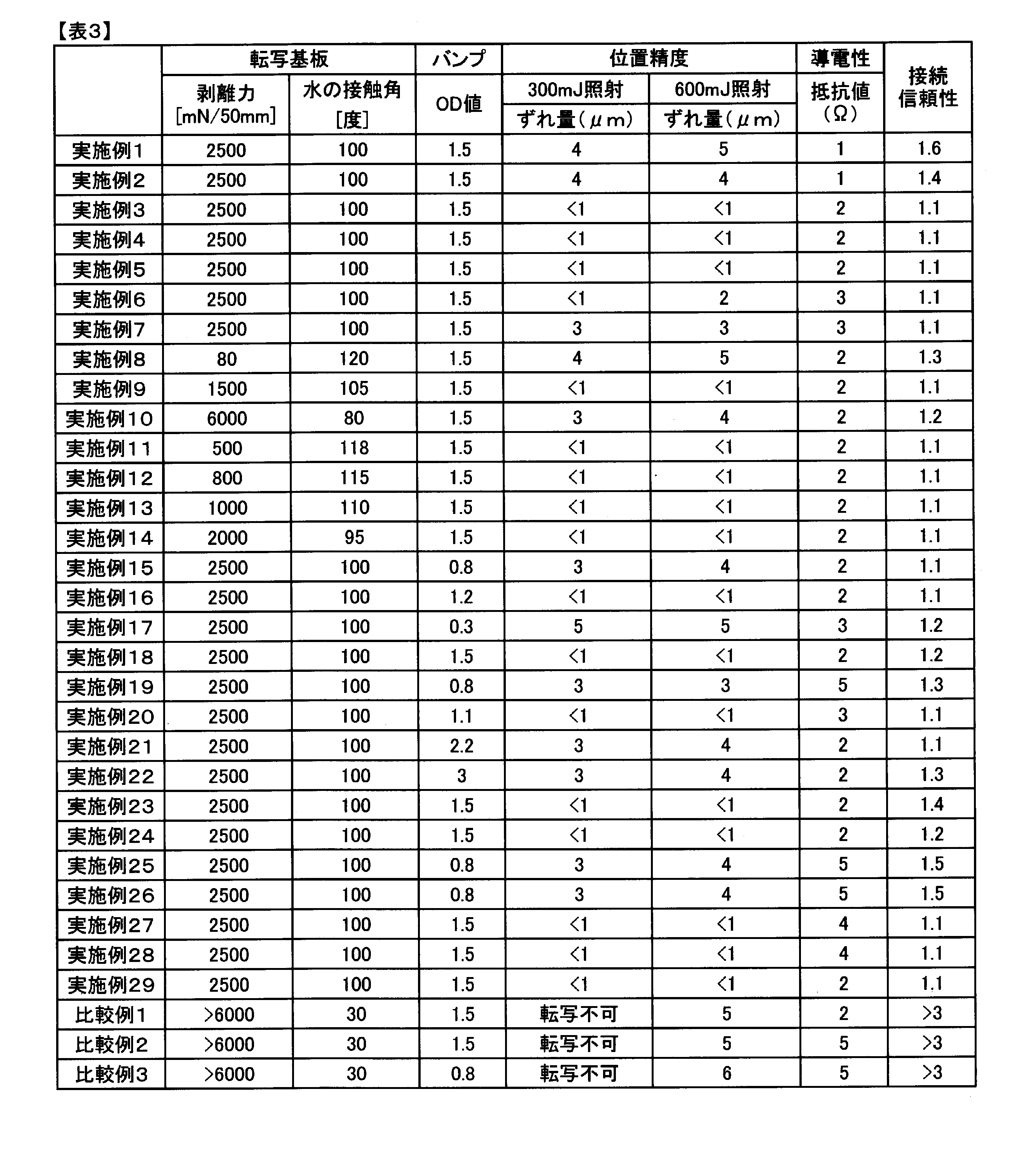
- the peeling force at 25° C. of the transfer substrate having a release layer is preferably 100 mN/50 mm or more from the viewpoint of maintaining appropriate adhesion between the bumps and the release layer and increasing the process margin in the bump transfer step.
- the peeling force at 25° C. of the transfer substrate having a release layer is preferably 5,000 mN/50 mm or less from the viewpoint of improving positional accuracy in the transfer process.
- the peeling force of the transfer substrate in the present invention means that an acrylic adhesive tape "31B" manufactured by Nitto Denko Co., Ltd. is applied to the release layer forming surface of the transfer substrate using a 2 kg roller, and left for 30 minutes.
- peeling force when the acrylic adhesive tape is peeled off at a temperature of 25° C., a peeling angle of 180°, and a peeling speed of 0.3 m/min As a means for setting the peeling force within the above range, for example, selecting one of the preferable mold release agents listed above may be mentioned.
- the water contact angle of the release layer at 25° C. is preferably 80 degrees or more, more preferably 90 degrees or more, from the viewpoint of increasing the process margin in the bump transfer step.
- the water contact angle of the release layer at 25° C. is preferably 140 degrees or less, more preferably 110 degrees or less, from the viewpoint of suppressing repellency and pinholes in the bump formation process and increasing the process margin in the bump transfer process.
- the water contact angle of the release layer can be measured in accordance with JIS R3257 (1999) using a commercially available contact angle measuring device such as "CA-Z" manufactured by Kyowa Interface Science Co., Ltd.
- Examples of methods for forming a bump pattern on the release layer include pattern printing, inkjet coating, laser etching, and photolithography.
- the pattern printing method is a method of printing an organic component and conductive particles on a release layer in a pattern using screen printing, gravure printing, or the like.
- the laser etching method is a method in which a rough pattern of organic components and conductive particles is printed and then unnecessary parts are removed using laser etching.
- a photosensitive composition is used as a composition containing an organic component and conductive particles, and a bump pattern is formed through a step of exposing the photosensitive composition (exposure step) and a step of developing it (developing step). This is a method of forming.
- the photolithography method is preferred from the viewpoint of enabling fine patterning and improving positional accuracy in the bump transfer process.
- i-line (365 nm) and h-line (405 nm) from a mercury lamp or LED are preferably used.
- Examples of the developer in the development step include tetramethylammonium hydroxide, diethanolamine, diethylaminoethanol, sodium hydroxide, potassium hydroxide, sodium carbonate, potassium carbonate, triethylamine, diethylamine, methylamine, dimethylamine, dimethylaminoethyl acetate, Examples include alkaline developers such as aqueous solutions of dimethylaminoethanol, dimethylaminoethyl methacrylate, cyclohexylamine, ethylenediamine, and hexamethylenediamine.
- the shape of the bump pattern is not particularly limited, but examples include rectangular, circular, elliptical, triangular, polygonal, and combinations of these in plan view.
- the thickness of the bump pattern in the bump forming step is preferably 1 ⁇ m or more from the viewpoint of further suppressing the occurrence of microcracks in the bump transfer step and further improving connection reliability.
- the thickness of the bump pattern is preferably 5 ⁇ m or less from the viewpoints of suppressing the spread of the bumps when electronic components are mounted, suppressing short circuits with surrounding electrodes, and improving positional accuracy in the bump transfer process.
- the thickness of the bump pattern in the bump forming process refers to the average value of the heights of 10 randomly selected bumps, which is calculated assuming that the pattern shape is rectangular. More specifically, 10 bump patterns randomly selected from the bump patterns formed in the bump formation process were examined at a magnification of 500 to 1,000 times using a laser microscope VK-X250 manufactured by Keyence Corporation. The surface is scanned with a laser and the shape of the surface is measured. Using the analysis mode attached to the device, the height of the bump pattern is calculated assuming that the pattern shape is rectangular, and the average value thereof is calculated, thereby making it possible to measure the thickness of the bump pattern.
- the aspect ratio of the bump pattern in the bump forming process is preferably 0.1 or more from the viewpoint of further suppressing the occurrence of microcracks in the bump transfer process and further improving connection reliability.
- the aspect ratio of the bump pattern is preferably 0.4 or less from the viewpoint of further enhancing the directivity in the bump transfer process and increasing the positional accuracy.
- the aspect ratio of the bump pattern in the bump forming process refers to the average value of the values obtained by dividing the bump pattern thickness by the bump pattern diameter for 10 randomly selected bump patterns. Note that if the bump has a cylindrical shape, the diameter is taken as the bump pattern diameter, and if the bump is not cylindrical, the diameter when converted to a cylinder having the same contact area is taken as the bump pattern diameter.
- the contact area between the bump pattern and the release layer in the bump forming step is preferably 25 ⁇ m 2 or more per bump pattern from the viewpoint of improving positional accuracy.
- the contact area between the bump pattern and the release layer is preferably 500 ⁇ m 2 or less from the viewpoint of uniformly causing ablation at the contact interface during laser irradiation and improving positional accuracy.
- the contact area between the bump and the release layer in the bump forming process refers to the average value of the contact area between 10 randomly selected bump patterns and the release layer. More specifically, an image of the bump pattern obtained by observing it using an optical microscope at a magnification of 500 to 1,000 times is analyzed using image analysis and measurement software, and the brightness of the measurement image is used as a standard.
- the dark area in the binarized image is defined as the contact area between the transfer substrate and the bump pattern, and the area of the dark area is calculated.
- the contact area with the release layer is calculated for 10 randomly selected bump patterns, and the average value thereof is taken as the contact area between the bump pattern and the release layer. Note that the contact area between the bump pattern and the release layer can be set within a desired range by adjusting the dimensions of the mask, for example, when forming the bump pattern by photolithography.
- the optical density (hereinafter referred to as "OD value”) of the bump pattern in the bump formation process limits the laser light that reaches the bump pattern to the vicinity of the release layer, increases the positional accuracy in the bump transfer process, and improves the process margin. From the viewpoint of widening the wavelength, it is preferably 0.5 or more, and more preferably 1 or more in the visible light range of wavelengths from 380 to 700 nm. On the other hand, the OD value of the bump pattern is preferably 3 or less from the viewpoint of connection reliability.
- the OD value of a bump pattern in the present invention refers to the average value of the OD values of five randomly selected bump patterns.
- I0 represents the incident light intensity
- I represents the transmitted light intensity.
- the bump contains an organic component and conductive particles.
- a photosensitive organic component examples include resins and monomers having photoreactive groups, photopolymerization initiators, and the like.
- organic components include acrylic copolymers, phenol novolac resins, cresol novolac resins, epoxy resins, urethane resins, polyimide resins, polyamic acids, polyamide resins, and siloxane resins.
- acrylic copolymers are preferred from the viewpoint of photosensitivity.
- the organic components include a combination of a carboxyl group-containing acrylic copolymer, a compound having a photoreactive group, and a photopolymerization initiator, a phenol novolac resin or a cresol novolak resin, Examples include a combination with a photoacid generator, a combination of a polyamic acid and a photoacid generator, a combination of a polyimide resin, a compound having a photoreactive group, and a photopolymerization initiator, and the like.
- a combination of a carboxyl group-containing acrylic copolymer, a compound having a photoreactive group, and a photopolymerization initiator is preferred, as it facilitates the formation of bumps with high mounting performance and a low glass transition temperature.
- the carboxyl group-containing acrylic copolymer has a photoreactive group, which has excellent photosensitivity and increases the crosslinking density in the exposed area, thereby increasing the strength of the bump and reducing microscopic particles in the bump transfer process. It is possible to further suppress the occurrence of cracks and further improve connection reliability.
- a carboxyl group-containing acrylic resin is produced by copolymerizing an acrylic monomer, which is a compound having a photoreactive group, and an unsaturated acid.
- acrylic monomers include methyl acrylate, ethyl acrylate (hereinafter sometimes referred to as "EA”), 2-ethylhexyl acrylate, n-butyl acrylate (hereinafter sometimes referred to as "BA”), iso-butyl acrylate, iso-propane acrylate, glycidyl acrylate, butoxytriethylene glycol acrylate, dicyclopentanyl acrylate, dicyclopentenyl acrylate, 2-hydroxyethyl acrylate, isobornyl acrylate, 2-hydroxypropyl acrylate, isodexyl Acrylate, isooctyl acrylate, lauryl acrylate, 2-methoxyethyl acrylate, methoxyethylene glycol acrylate, methoxydi
- the content of the carboxyl group-containing acrylic resin in the organic component is preferably 20 to 70% by weight based on the solid content.
- the solid content refers to components other than the solvent in the organic component.
- an acrylic monomer is preferable, and examples thereof include the acrylic monomers exemplified as raw materials for the above-mentioned carboxyl group-containing acrylic resin.
- the content of the compound having a photoreactive group in the organic component is preferably 5 to 30% by weight based on the solid content.
- the content of the compound having a photoreactive group is 5% by weight or more, the cure density of the exposed area increases, so that the residual film rate after development can be increased and fine patterning becomes possible.
- the content of the compound having a photoreactive group is 30% by weight or less, the bump pattern to be formed does not become too hard, and the adhesion with electronic components improves, increasing connection reliability.
- benzophenone derivatives As photopolymerization initiators, benzophenone derivatives, acetophenone derivatives, thioxanthone derivatives, benzyl derivatives, benzoin derivatives, oxime compounds, ⁇ -hydroxyketone compounds, ⁇ -aminoalkylphenone compounds, phosphine oxide compounds, anthrone compounds, Examples include anthraquinone compounds. Among these, oxime compounds with high photosensitivity are preferred.
- oxime compounds include 1,2-octanedione-1-[4-(phenylthio)-2-(O-benzoyloxime)], ethanone-1-[9-ethyl-6-(2-methylbenzoyl) )-9H-carbazol-3-yl]-1-(O-acetyloxime), 1-phenyl-1,2-butanedione-2-(O-methoxycarbonyl)oxime, 1-phenyl-propanedione-2-( O-ethoxycarbonyl)oxime, 1-phenyl-propanedione-2-(O-benzoyl)oxime, 1,3-diphenyl-propanedione-2-(O-ethoxycarbonyl)oxime, 1-phenyl-3-ethoxy- Examples include propanetrione-2-(O-benzoyl)oxime. Two or more types of these may be contained.
- the content of the photopolymerization initiator in the organic component is preferably 1 to 10% by weight based on the solid content.
- the content of the photopolymerization initiator is 1% by weight or more, the cured density of the exposed area increases, so the residual film rate after development can be increased, and fine patterning becomes possible.
- the content of the photopolymerization initiator is 10% by weight or less, side edges due to excessive light absorption by the photopolymerization initiator at the top of the coated dry film during exposure are suppressed, improving microprocessability and laser transfer. Positional accuracy can be further improved.
- the epoxy compound examples include glycidyl ethers, glycidyl amines, and epoxy resins. More specifically, the glycidyl ethers include, for example, methyl glycidyl ether, ethyl glycidyl ether, butyl glycidyl ether, ethylene glycol diglycidyl ether, diethylene glycol diglycidyl ether, propylene glycol diglycidyl ether, tripropylene glycol diglycidyl ether, Neopentyl glycol diglycidyl ether, bisphenol A diglycidyl ether, hydrogenated bisphenol A diglycidyl ether, bisphenol F diglycidyl ether, bisphenol S diglycidyl ether, bisphenol fluorene glycidyl ether, biphenol diglycidyl ether, tetramethylbiphenol glycidyl ether, Examples include trimethylolpropane triglycidy
- Examples of glycidylamines include tert-butylglycidylamine.
- Examples of the epoxy resin include bisphenol A epoxy resin, bisphenol F epoxy resin, biphenyl epoxy resin, novolac epoxy resin, and hydrogenated bisphenol A epoxy resin. Two or more types of these may be used.
- the content of the epoxy compound in the organic component is preferably 5 to 50% by weight based on the solid content.
- the content of the epoxy compound is 5% by weight or more, the adhesion between the board and the electronic component improves, and the connection reliability increases.
- the content of the epoxy compound is 50% or less, the photocuring reaction during exposure will proceed smoothly and the crosslinking density will increase, making it possible to form a fine pattern.
- the conductive particles form a three-dimensional conductive path after mounting, and high conductivity is exhibited.
- conductive particles include metals such as silver, gold, copper, platinum, lead, tin, nickel, aluminum, tungsten, molybdenum, chromium, titanium, and indium, and alloys thereof, ITO, tin oxide, and antimony-doped tin oxide. , carbon black, and the like.
- examples include those having a coating layer of the aforementioned metal or carbon on the surface of insulating particles or conductive particles such as resin or inorganic oxide. Two or more types of these may be contained.
- Carbon black or metal particles with a carbon coating are preferred. Furthermore, carbon black is preferable because it can establish stable electrical connections with molybdenum and ITO, which are considered difficult to establish electrical connections with.
- the aspect ratio of the conductive particles is preferably 1.0 or more from the viewpoint of increasing the probability of contact between the conductive particles.
- the aspect ratio of the conductive particles is preferably 3.0 or less, more preferably 2.0 or less, from the viewpoint of suppressing shielding of exposure light in the exposure step and widening the development margin in the development step.
- the aspect ratio of the conductive particles is a value obtained by dividing the long axis length of the conductive particles by the short axis length.
- conductive particles were observed under magnification at a magnification of 15,000 times, and each of the primary particles of 100 randomly selected conductive particles was The long axis length and short axis length of the conductive particles are measured, and the number average value of the aspect ratio obtained from both is taken as the aspect ratio of the conductive particles.
- the particle diameter of the conductive particles is preferably 0.03 ⁇ m or more from the viewpoint of dispersibility in the photosensitive composition.
- the particle diameter of the conductive particles is preferably 1.0 ⁇ m or less, more preferably 0.2 ⁇ m or less, from the viewpoint of further improving the surface smoothness, pattern accuracy, and dimensional accuracy of the bump, and the positional accuracy in the bump transfer process.
- the particle diameter of the conductive particles can be determined by a dynamic light scattering method. Specifically, a dispersion liquid with a conductive particle concentration of 5 to 30% by volume is irradiated with light at a wavelength of 780 nm using a semiconductor laser, the scattered light is measured, and then frequency analysis is performed using the FFT-heterodyne method. be able to.
- the content of conductive particles in the bump is preferably 10% by volume or more, more preferably 15% by volume or more, from the viewpoint of improving conductivity.
- the content of conductive particles is determined from the viewpoints of containing an appropriate amount of organic components to further improve the positional accuracy in the bump transfer process, further mitigating the impact in the bump transfer process and improving connection reliability, and From the viewpoint of improving the bonding strength between the component and the structure with bumps, the content is preferably 40% by volume or less, and more preferably 30% by volume or less.
- the content of conductive particles in the bump can be measured as follows.
- the bumps on the transfer substrate are scraped off and used as measurement samples.
- the measurement sample is held in the atmosphere at 600°C for 1 hour using a thermogravimetric analyzer to remove organic components, and the weight ratio of the remaining portion of the measurement sample (thermogravimetric analysis residual ratio) and measurement sample are The proportion of the weight of the removed portion (thermogravimetric analysis reduction rate) is determined.
- Calculate the content (volume %) of conductive particles in the bump using the following formula [1], using the thermogravimetric analysis residual fraction as the weight fraction of the conductive particles and the thermogravimetric analysis reduction rate as the weight fraction of the organic component. can do.
- the density of the organic component is 1.1 g/cm 3 .
- the content (volume %) of the conductive particles in the bump can be calculated from the composition ratio.
- Bumps and the photosensitive composition used to form bumps may contain additives such as plasticizers, leveling agents, surfactants, silane coupling agents, antifoaming agents, pigments, etc., to the extent that their desired properties are not impaired. You may.
- this step also applies to the transfer substrate, release layer, and bump pattern of the substrate having a bump pattern, which is the second aspect of the present invention. Further, this step also corresponds to a method for manufacturing a substrate having a bump pattern, which is the second aspect of the present invention.
- a laser is irradiated from the side opposite to the release layer of the transfer substrate to transfer the bumps to the electrode-equipped substrate or the electrode portion of the electronic component.
- the organic components and conductive particles contained in the bumps are heated by the laser light transmitted through the transfer substrate, and the organic components of the bumps at the interface of the release layer of the transfer substrate are decomposed, causing the bumps to separate from the release layer. It is transferred to a substrate with electrodes or an electrode part of an electronic component.
- the transferability is excellent even when the laser irradiation intensity is low, so it is possible to suppress the decomposition of organic substances and the impact of bumps due to laser irradiation, and the bumps have high connection reliability. can be formed.
- the laser used for irradiation may be any laser that can decompose the organic components at the interface of the transfer substrate by the heat generated by the irradiation, and examples thereof include a laser with a wavelength range of 257 to 1900 nm. Among these, a solid-state laser with a wavelength of 355 nm or 532 nm is preferable from the viewpoint of transferability.
- the output of the laser is preferably 200 to 600 mJ. When the laser output is 200 mJ or more, it is less susceptible to variations in the adhesion between the bump and the release layer, and the positional accuracy in the transfer process can be improved. On the other hand, if the laser output is 600 mJ or less, the impact in the bump transfer process can be further alleviated and connection reliability can be further improved.
- the laser output is more preferably 500 mJ or less.
- the contact area between the bump and the electrode-attached substrate or electronic component onto which the bump is transferred is preferably 20 ⁇ m 2 or more on average per bump from the viewpoint of further increasing the positional accuracy in the bump transfer process.
- the contact area is preferably 500 ⁇ m 2 or less from the viewpoint of suppressing temperature unevenness of the bump due to laser irradiation and improving positional accuracy.
- the contact area between a bump and an electrode-attached substrate or an electronic component in the present invention refers to an average value of 10 randomly selected bumps. Using an optical microscope, a board with electrodes or electronic components including bumps is observed and photographed at a magnification of 500 to 1,000 times, and the obtained image is converted into a measurement image using image analysis and measurement software.
- the area of the dark part is calculated by assuming that the dark part in the binarized image corresponds to the contact part between the electrode-equipped substrate or the electronic component and the bump.
- the contact area is calculated for 10 randomly selected bumps, and the average value is taken as the contact area between the electrode-equipped substrate or electronic component and the bump. For example, when forming bumps by photolithography, the contact area can be adjusted to a desired range by adjusting the dimensions of the mask.
- a TFT substrate with electrodes made of a material selected from molybdenum, titanium, and ITO, a printed wiring board with copper electrodes, etc. are preferable.
- the electronic component to which the bumps are transferred is preferably an LED chip having a gold electrode.
- the electrode with which the transferred bump comes into contact preferably contains a material selected from molybdenum, titanium, and ITO, since ion migration and generation of intermetallic compounds are small. Electrodes containing these have high connection reliability with carbon black, and are therefore preferably used when carbon black is used as the conductive particles contained in the bumps.
- FIG. 2 shows a schematic diagram of an application example of the method for manufacturing a bumped structure of the present invention.
- a transfer substrate 13 which is a substrate with electrodes
- specific electronic components 14' may be confirmed to be defective.
- a repair operation is performed in which the defective electronic component 14' is removed and a new electronic component is mounted in its place.
- a transfer substrate 11 having a release layer 5 on which bumps 10 are formed is used, and by irradiating the laser 12, as shown in FIG. ), bumps can be formed only in the defective portion of the electronic component 14'. That is, bumps can be formed on the transfer substrate 13 on which the electronic components 14 are mounted without being affected by the unevenness caused by the electronic components 14.
- the method for manufacturing a structure with bumps and the substrate having a bump pattern of the present invention can be suitably used, for example, when manufacturing a substrate for mounting an LED.
- the substrate having the bump pattern of the present invention can be suitably used for the above-mentioned repair applications.
- the evaluation method in each example is as follows.
- ⁇ Water contact angle of release layer> The release layer of the transfer substrate produced in each Example and Comparative Example was measured at 25°C in accordance with JIS R3257 (1999) using a contact measurement device "CA-Z" manufactured by Kyowa Interface Science Co., Ltd. Water contact angle was measured.
- a 3 mm square silicon chip with electrodes was bonded by thermocompression for 5 seconds at a temperature of 120°C and a pressure of 1 MPa on the printed wiring board with bumps obtained in each example and comparative example. Heated at 140°C for 30 minutes.
- a silicon chip mounting board was produced, as shown in FIG. 4, in which electrodes 9 of silicon chips 8 were bonded to electrodes 7 of printed wiring board 6 having bumps 1. Thereafter, points a and b of the printed wiring board with bumps were connected with a tester, and the resistance value was measured.
- Mold agent KTS-3000H Fluorine mold release agent manufactured by AGC Seimi Chemical Co., Ltd.
- SR-4000A Fluorine mold release agent manufactured by AGC Seimi Chemical Co., Ltd.
- "Piroil (registered trademark)" 1010 Lion Specialty Long-chain alkyl mold release agent manufactured by Chemicals Co., Ltd.
- ⁇ Tin oxide particles Tin-based oxide particles manufactured by Mitsubishi Materials Electronic Chemicals Co., Ltd.
- N-770 Phenol novolac type epoxy resin manufactured by DIC Corporation (hereinafter referred to as N-770).
- EA ethyl acrylate
- 2-EHMA 2-ethylhexyl methacrylate
- BA n-butyl acrylate
- a mixture consisting of "AA”, 0.8 g of 2,2'-azobisisobutyronitrile, and 10 g of PGMEA was added dropwise over 1 hour. After the addition was completed, the polymerization reaction was further heated at 80°C for 6 hours. Thereafter, 0.2 g of hydroquinone monomethyl ether was added to stop the polymerization reaction.
- Example 1 A 5% by weight toluene solution of silicone mold release agent "Tesfine (registered trademark)" 303 was applied onto a glass substrate using a spin coater at a rotation speed of 2,000 rpm, and then coated at 140°C for 30 minutes using a drying oven. This was heated to produce a transfer substrate 1 having a release layer.
- silicone mold release agent "Tesfine (registered trademark)" 303 was applied onto a glass substrate using a spin coater at a rotation speed of 2,000 rpm, and then coated at 140°C for 30 minutes using a drying oven. This was heated to produce a transfer substrate 1 having a release layer.
- the photosensitive composition 1 is applied in a pattern to have a diameter of 100 ⁇ m and a thickness of 2 ⁇ m after drying using an inkjet coating device to form a bump pattern. did. A total of 100 bump patterns were fabricated within a 3 mm square area on the transfer substrate 1, with 10 bump patterns in each direction. Thereafter, it was dried at 100° C. for 10 minutes using a drying oven. The contact area with the transfer substrate 1 per bump pattern was 7,850 ⁇ m 2 .
- the transfer substrate 1 on which the bump pattern has been formed and the glass substrate for transfer, on which a cross mark has been marked in advance at a desired position are made to face each other so that the distance between the substrates is 50 ⁇ m, and the glass substrate for transfer is placed so that the distance between the substrates is 50 ⁇ m.
- Positioning was performed so that the intersection of the cross marks overlapped with the center of the bump, and laser irradiation was performed from the back side of the transfer substrate 1.
- the laser had a wavelength of 532 nm, a beam size 1.5 times that of the bump, and irradiation was performed at two levels of energy, 300 mJ and 600 mJ.
- the bumps on the transfer substrate 1 were transferred to the glass substrate to be transferred, and a glass substrate with bumps was obtained. Using the obtained glass substrate with bumps, positional accuracy was evaluated by the method described above.
- Example 2 The photosensitive composition 1 prepared in Example 1 was applied onto the transfer substrate 1 prepared in Example 1 so that the film thickness after drying was 2 ⁇ m, and the film was heated at 100° C. for 10 minutes using a drying oven. Dry. Thereafter, through a mask corresponding to a pattern to be described later, exposure was performed using an exposure machine at an exposure amount of 1,000 mJ/cm 2 , and alkali development was performed to form a bump pattern.
- Each bump pattern had a diameter of 100 ⁇ m, and a total of 100 bump patterns were prepared within a 3 mm square area on the transfer substrate 1, with 10 bump patterns in each direction.
- the contact area with the transfer substrate 1 per bump pattern was 7,850 ⁇ m 2 .
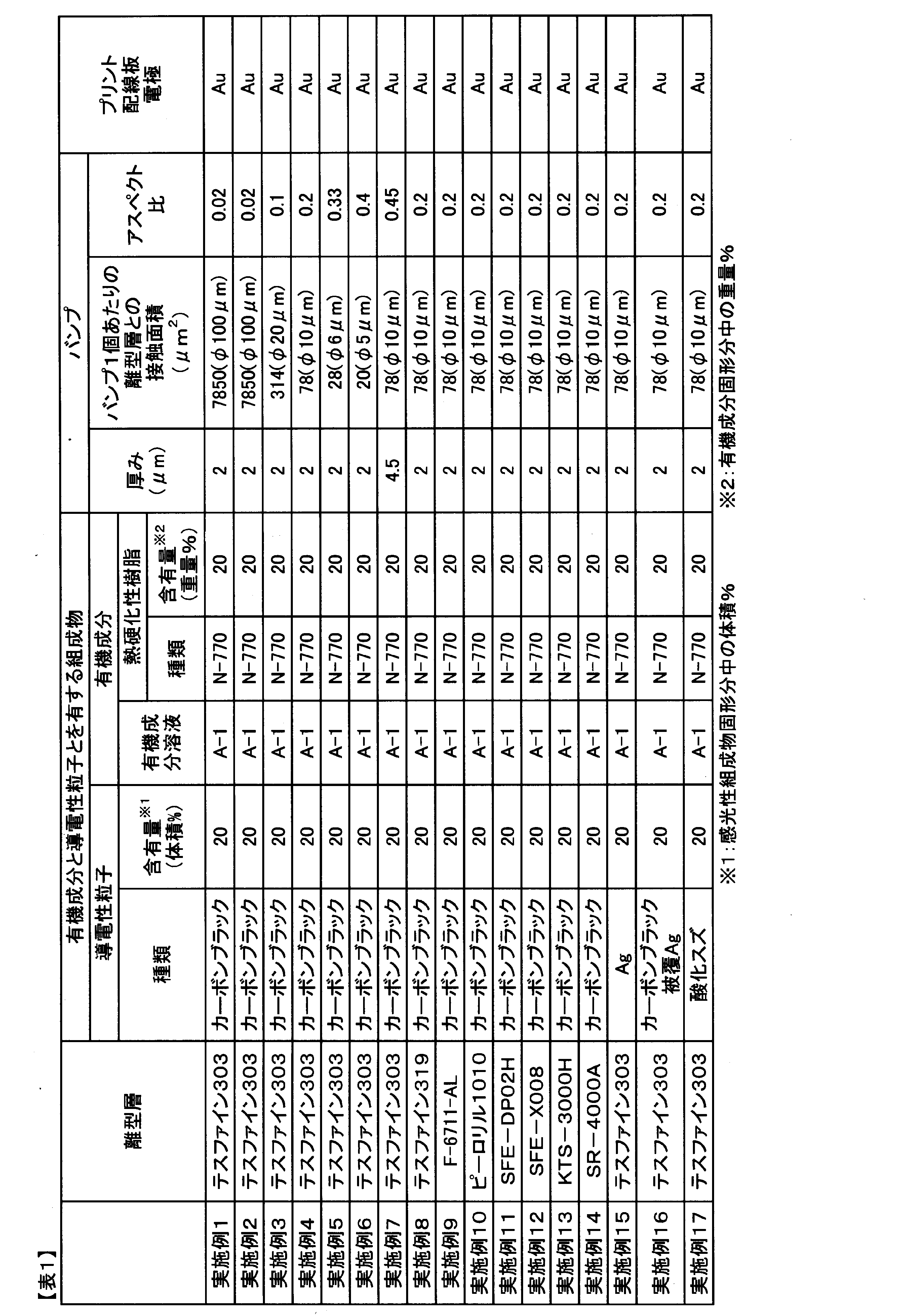
- Examples 3 to 6 A glass substrate with bumps and a printed wiring board with bumps were prepared in the same manner as in Example 2, except that the diameter of the bumps was changed and the contact area with the release layer per bump was changed as shown in Table 1. It was prepared and evaluated.
- Example 7 A glass substrate with bumps and a printed wiring board with bumps were produced and evaluated in the same manner as in Example 4, except that the thickness of the bumps was changed as shown in Table 1.
- Example 8 to 14 A glass substrate with bumps and A printed wiring board with bumps was produced and evaluated.
- Example 15 to 17 In place of the carbon black dispersion B-1 obtained in Synthesis Example 3, Ag particle dispersion B-2 obtained in Synthesis Examples 4 to 6, carbon-coated Ag dispersion B-3, and tin oxide dispersion B-4 were used. A glass substrate with bumps and a printed wiring board with bumps were produced and evaluated in the same manner as in Example 4, except that each of the following was used.
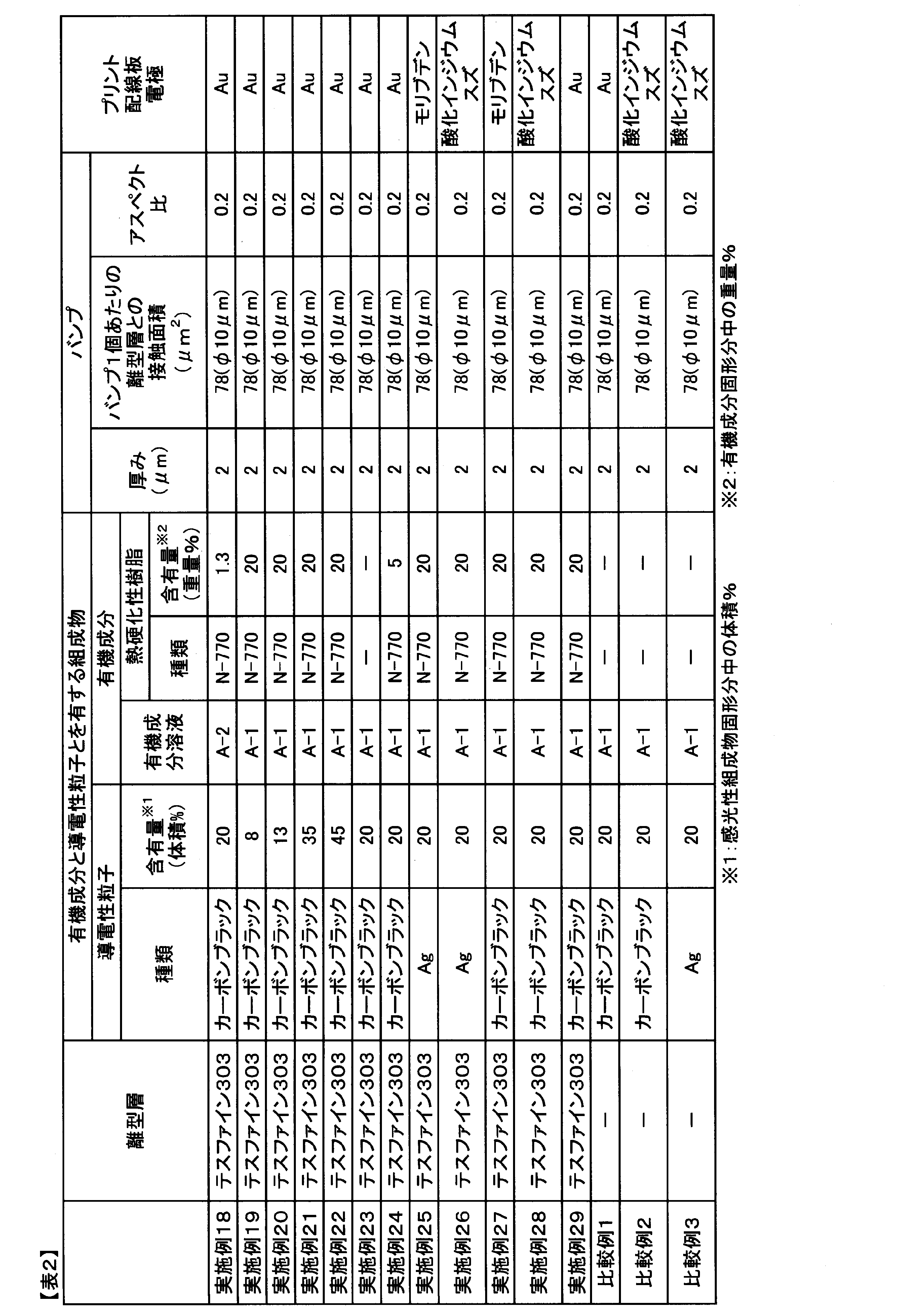
- Example 18 A glass substrate with bumps and a print with bumps were prepared in the same manner as in Example 4, except that organic component solution A-2 obtained in Synthesis Example 2 was used instead of organic component solution A-1 obtained in Synthesis Example 1. A wiring board was produced and evaluated.
- Example 19-24 Bumped glass was prepared in the same manner as in Example 4, except that the conductive particle content in carbon black dispersion B-1 and the thermosetting resin content in organic component solution A-1 were changed as shown in Table 2. A substrate and a printed wiring board with bumps were fabricated and evaluated.
- Example 25-26 A glass substrate with bumps and a printed wiring board with bumps were prepared and evaluated in the same manner as in Example 15, except that the electrodes of the printed wiring board were changed as shown in Table 2.
- Example 27-28 A glass substrate with bumps and a printed wiring board with bumps were prepared and evaluated in the same manner as in Example 4, except that the electrodes of the printed wiring board were changed as shown in Table 2.
- Example 29 After mounting a silicon chip with electrodes for conductivity evaluation on a printed wiring board prepared in the same manner as in Example 4, a new printed wiring board with bumps was placed next to the mounted silicon chip in the same manner as in Example 4. was prepared and evaluated.
- Example 1 A glass substrate with bumps and a printed wiring board with bumps were produced and evaluated in the same manner as in Example 23 except that a release layer was not provided.
Landscapes
- Engineering & Computer Science (AREA)
- Microelectronics & Electronic Packaging (AREA)
- Manufacturing & Machinery (AREA)
- Wire Bonding (AREA)
- Manufacturing Of Printed Wiring (AREA)
- Electric Connection Of Electric Components To Printed Circuits (AREA)
Abstract
Description
前記転写基板の離型層の反対面側からレーザーを照射して、電極付き基板または電子部品の電極部へ、前記バンプを転写する工程(バンプ転写工程)
を有するバンプ付き構造物の製造方法である。
離型層を有する転写基板の離型層上に、有機成分および導電性粒子を含有するバンプ(バンプパターン)を形成する。
OD値 = log10(I0/I) (1)
ここで、I0は入射光強度、Iは透過光強度を示す。

次に、転写基板の離型層の反対面側からレーザーを照射して、電極付き基板または電子部品の電極部へ、バンプを転写する。本工程において、転写基板を透過したレーザー光により、バンプに含まれる有機成分および導電性粒子が加熱され、転写基板の離型層界面にあるバンプの有機成分が分解し、バンプが離型層から電極付き基板または電子部品の電極部へ転写される。
各実施例および比較例において、転写基板の離型層上にバンプを形成した後、無作為に選択した10個のバンプを、(株)キーエンス社製マイクロスコープVHX-5500を用いて、倍率500~1,000倍で撮影し、画像解析モードにより、測定用画像の明度を基準として2値化した。該2値化画像における暗部を、それぞれのバンプと離型層の接触部に相当するとして、該暗部の面積を算出した。10個のバンプについての暗部の面積の平均値を算出することにより、バンプ一つ当たりの離型層との接触面積を求めた。
各実施例および比較例において作製した転写基板の離型層に、2kgローラーを用いて、日東電工(株)製アクリル粘着テープ「31B」を貼付し、30分間静置した後に、温度25℃、剥離角度180°、剥離速度0.3m/分の条件で、該粘着テープを剥離したときの剥離力を測定した。
各実施例および比較例において作製した転写基板の離型層について、協和界面化学(株)製接触確測定装置「CA-Z」を用いて、JIS R3257(1999年)に準拠して25℃における水接触角を測定した。
各実施例および比較例において、転写基板の離型層上にバンプを形成した後、無作為に選択した5個のバンプについて、顕微分光器(日本分光(株)製 MSV-5500)を用いて、波長532nmの透過光強度を測定し、透過光強度からそれぞれのバンプのOD値を求めた。5個のバンプについて、その平均値を算出し、バンプのOD値とした。
各実施例および比較例により得られたバンプ付きガラス基板から無作為に選択した10個のバンプについて、バンプが形成された面とは反対側の面より光学顕微鏡を用いてバンプを観察し、バンプの中心と、被転写物の十字マークの交点とのずれ量を測定した。10個のバンプについて、その平均値を算出した。なお、300mJ照射時と600mJ照射時のすれ量の差が小さいほど、プロセスマージンが高いといえる。
各実施例および比較例により得られたバンプ付きプリント配線板上に、電極を有する3mm角のシリコンチップを、温度120℃、圧力1MPaの条件で5秒間熱圧着した後、オーブンを用いて、温度140℃で30分間加熱した。これにより、図4に示す、バンプ1を有するプリント配線板6の電極7上に、シリコンチップ8の電極9が接合したシリコンチップ実装基板を作製した。その後、バンプ付きプリント配線板のa点とb点をテスターでつなぎ、抵抗値を測定した。
前述の<導電性>評価において作製したシリコンチップ実装基板を、-55℃と125℃の環境下においてそれぞれ1時間ずつ静置する加熱冷却工程を1サイクルとして500サイクル実施した後、前述の<導電性>と同様に抵抗値を測定した。下記式により加熱冷却工程前後の抵抗値変化を算出し、接続信頼性を評価した。抵抗値変化が1に近いほど、接続信頼性が高いといえる。
抵抗値変化=加熱冷却後の抵抗値/加熱冷却前の抵抗値。
[離型剤]
・“テスファイン(登録商標)”303:昭和電工マテリアルズ(株)製アミノアルキド系離型剤
・“テスファイン(登録商標)”319:昭和電工マテリアルズ(株)製シリコーン系離型剤
・F-6711-AL:AGCセイミケミカル(株)製フッ素系離型剤
・SFE-DP02H:AGCセイミケミカル(株)製フッ素系離型剤
・SFE-X008:AGCセイミケミカル(株)製フッ素系離型剤
・KTS-3000H:AGCセイミケミカル(株)製フッ素系離型剤
・SR-4000A:AGCセイミケミカル(株)製フッ素系離型剤
・“ピーロイル(登録商標)”1010:ライオン・スペシャリティ・ケミカルズ(株)製長鎖アルキル系離型剤
[導電性粒子]
・Ag粒子:DOWAエレクトロニクス(株)製Ag粒子(平均粒子径300nm、比重10g/cm3)
・酸化スズ粒子:三菱マテリアル電子化成(株)製スズ系酸化物粒子(体積平均粒子径300nm、比重7.0g/cm3)
・カーボンブラック粒子:Cabot社製カーボンブラック粒子(平均粒子径50nm、比重1.9g/cm3)
・炭素被覆Ag粒子:日清エンジニアリング(株)製カーボン被覆Ag粒子(表面炭素被覆層の平均厚み1nm、平均粒子径40nm、比重9.5g/cm3)
[熱硬化性樹脂]
・EPICLON(登録商標) N-770:DIC(株)製フェノールノボラック型エポキシ樹脂(以下、N-770と称す)。
窒素雰囲気の反応容器中に、150gのプロピレングリコールモノメチルエーテルアセテート(以下、「PGMEA」)を仕込み、オイルバスを用いて80℃まで昇温した。これに、20gのエチルアクリレート(以下、「EA」)、40gのメタクリル酸2-エチルヘキシル(以下、2-EHMA)、20gのn-ブチルアクリレート(以下、BA)、15gのアクリル酸(以下、「AA」、0.8gの2,2’-アゾビスイソブチロニトリルおよび10gのPGMEAからなる混合物を、1時間かけて滴下した。滴下終了後、さらに80℃で6時間加熱して重合反応を行った。その後、0.2gのハイドロキノンモノメチルエーテルを添加して、重合反応を停止した。引き続き、5gのグリシジルメタクリレート、1gのトリエチルベンジルアンモニウムクロライドおよび10gのPGMEAからなる混合物を、0.5時間かけて滴下した。滴下終了後、さらに2時間加熱して付加反応を行った。その後、反応容器内を大気雰囲気にして5gの光重合開始剤“Irgacure(登録商標)”OXE03(BASF社製)および20gのアクリル系モノマー“アロニックス(登録商標)”M-315(東亜合成(株)製)を添加して50℃で3時間加熱溶解して、固形分42.8重量%の有機成分溶液(A-1)を得た。
窒素雰囲気の反応容器中に、150gのPGMEAを仕込み、オイルバスを用いて80℃まで昇温した。これに、20gのEA、20gの2-EHMA、20gのBA、5gのメチロールアクリルアミド、25gのAA、0.8gの2,2’-アゾビスイソブチロニトリルおよび10gのPGMEAからなる混合物を、1時間かけて滴下した。滴下終了後、さらに80℃で6時間加熱して重合反応を行った。その後、0.2gのハイドロキノンモノメチルエーテルを添加して、重合反応を停止した。反応容器内を大気雰囲気にした後、5gの光重合開始剤“Irgacure”OXE03(BASF社製)、20gのアクリルモノマー“アロニックス(登録商標)”M-315(東亜合成(株)製)を添加して50℃で3時間加熱溶解して、固形分42.0重量%の有機成分溶液(A-2)を得た。
13.7gのカーボンブラック粒子、4gの分散剤“DISPERBYK(登録商標)”-21116(ビックケミー社製)および200gのPGMEAを混合し、ホモジナイザーを用いて、1,200rpm、30分間の混合処理を施した。その後、さらに、高圧湿式メディアレス微粒化装置“ナノマイザー”(ナノマイザー(株))を用いて分散処理し、平均粒子径0.15μm、導電性粒子含有量6.3重量%のカーボンブラック分散液B-1を得た。
80gのAg粒子、4gの分散剤“DISPERBYK(登録商標)”-21116(ビックケミー社製)および200gのPGMEAを混合し、ホモジナイザーを用いて、1,200rpm、30分間の混合処理を施した。その後、さらに、高圧湿式メディアレス微粒化装置“ナノマイザー”(ナノマイザー(株))を用いて分散処理して、平均粒子径0.6μm、導電性粒子含有量28.2重量%のAg粒子分散液B-2を得た。
80gのカーボン被覆Ag粒子、4gの分散剤“DISPERBYK(登録商標)”-21116(ビックケミー社製)および200gのPGMEAを混合し、ホモジナイザーを用いて、1,200rpm、30分間の混合処理を施した。その後、さらに、高圧湿式メディアレス微粒化装置“ナノマイザー”(ナノマイザー(株))を用いて分散処理して、平均粒子径0.2μm、導電性粒子含有量28.2重量%のカーボン被覆Ag分散液B-3を得た。
40gの酸化スズ粒子、4gの分散剤“DISPERBYK(登録商標)”-21116(ビックケミー社製)および200gのPGMEAを混合し、ホモジナイザーを用いて、1200rpm、30分間の混合処理を施した。その後、さらに、高圧湿式メディアレス微粒化装置“ナノマイザー”(ナノマイザー(株))を用いて分散処理して、平均粒子径0.2μm、導電性粒子含有量16.4重量%の酸化スズ分散液B-4を得た。
ガラス基板上に、シリコーン系離型剤“テスファイン(登録商標)”303の5重量%トルエン溶液を、2,000rpmの回転数でスピンコーター塗布した後、乾燥オーブンを用いて140℃で30分間加熱し、離型層を有する転写基板1を作製した。
実施例1において作製した転写基板1上に、実施例1において作製した感光性組成物1を、乾燥後の膜厚が2μmになるように塗布し、乾燥オーブンを用いて、100℃で10分間乾燥した。その後、後述するパターンに対応するマスクを介して、露光機により露光量1,000mJ/cm2で露光し、アルカリ現像を行い、バンプパターンを形成した。バンプパターンは、1個あたり直径100μmの寸法とし、転写基板1上の3mm角のエリア内に縦横10個ずつ、合計100個作製した。バンプパターン1個当たりの転写基板1との接触面積は、7,850μm2であった。
バンプの径を変更してバンプ1個当たりの離型層との接触面積を表1に記載の通りに変更したこと以外は実施例2と同様にしてバンプ付きガラス基板およびバンプ付きプリント配線板を作製して評価した。
バンプの厚みを表1に記載の通りに変更したこと以外は実施例4と同様にしてバンプ付きガラス基板およびバンプ付きプリント配線板を作製して評価した。
ガラス基板上に、シリコーン系離型剤“テスファイン(登録商標)”303にかえて表1に記載の材料により離型層を形成したこと以外は実施例4と同様にしてバンプ付きガラス基板およびバンプ付きプリント配線板を作製して評価した。
合成例3により得られたカーボンブラック分散液B-1にかえて合成例4~6により得られたAg粒子分散液B-2、カーボン被覆Ag分散液B-3および酸化スズ分散液B-4をそれぞれ用いたこと以外は実施例4と同様にしてバンプ付きガラス基板およびバンプ付きプリント配線板を作製して評価した。
合成例1により得られた有機成分溶液A-1にかえて合成例2により得られた有機成分溶液A-2を用いたこと以外は実施例4と同様にしてバンプ付きガラス基板およびバンプ付きプリント配線板を作製して評価した。
カーボンブラック分散液B-1における導電性粒子含有量および有機成分溶液A-1における熱硬化性樹脂含有量を表2に記載のとおりに変更したこと以外は実施例4と同様にしてバンプ付きガラス基板およびバンプ付きプリント配線板を作製して評価した。
プリント配線板の電極を表2に記載のとおりに変更したこと以外は実施例15と同様にしてバンプ付きガラス基板およびバンプ付きプリント配線板を作製して評価した。
プリント配線板の電極を表2に記載のとおりに変更したこと以外は実施例4と同様にしてバンプ付きガラス基板およびバンプ付きプリント配線板を作製して評価した。
実施例4と同様の方法により作製したプリント配線板に導電性評価用の電極付きシリコンチップを実装した後、実装されたシリコンチップの横に新たに実施例4と同様にしてバンプ付きプリント配線板を作製して評価した。
離型層を設けないこと以外は実施例23と同様にしてバンプ付きガラス基板およびバンプ付きプリント配線板を作製して評価した。
離型層を設けないこと以外は実施例28および実施例26とそれぞれ同様にしてバンプ付きガラス基板およびバンプ付きプリント配線板を作製して評価した。
2:ガラス基板
3:レーザー
4:被転写基板
5:離型層
6:プリント配線板
7:プリント配線板の電極
8:シリコンチップ
9:シリコンチップの電極
10:バンプ
11:転写基板
12:レーザー
13:被転写基板
14、14’:電子部品
15:電子部品の電極
Claims (11)
- 離型層を有する転写基板の離型層上に、有機成分および導電性粒子を含有するバンプパターンを有する基板。
- 前記離型層を有する転写基板の25℃における剥離力が100~5,000mN/50mmである請求項1記載の基板。
- 前記バンプパターン中の導電性粒子の含有量が10~40体積%である請求項1または2記載の基板。
- 前記バンプパターンのOD値が0.5~3である請求項1または2記載の基板。
- 前記バンプパターンのアスペクト比が0.1~0.4であり、バンプパターン1個あたりの離型層との接触面積が25~500μm2である請求項1または2記載の基板。
- 前記導電性粒子として、カーボンブラックおよび/または炭素被覆層を有する金属粒子を含む請求項1または2記載の基板。
- リペア用である請求項1または2記載の基板。
- 有機成分および導電性粒子を含有する感光性組成物を露光する工程(露光工程)および現像する工程(現像工程)を有する請求項1または2記載の基板の製造方法。
- 請求項1または2に記載の基板の離型層の反対面側からレーザーを照射して、電極付き基板または電子部品の電極部へ、バンプを転写する工程(バンプ転写工程)を有するバンプ付き構造物の製造方法。
- 前記電極付き基板が、電子部品が実装されてなる電極付き基板である請求項9に記載のバンプ付き構造物の製造方法。
- 離型層を有する転写基板の離型層上に、有機成分および導電性粒子を含有するバンプを形成する工程(バンプ形成工程)、および、前記転写基板の離型層の反対面側からレーザーを照射して、電極付き基板または電子部品の電極部へ、前記バンプを転写する工程(バンプ転写工程)を有するバンプ付き構造物の製造方法。
Priority Applications (3)
| Application Number | Priority Date | Filing Date | Title |
|---|---|---|---|
| KR1020247037949A KR20250028244A (ko) | 2022-06-28 | 2023-06-14 | 범프 구비 구조물의 제조 방법 및 범프 패턴을 갖는 기판 |
| JP2023537257A JPWO2024004652A1 (ja) | 2022-06-28 | 2023-06-14 | |
| CN202380037807.XA CN119138109A (zh) | 2022-06-28 | 2023-06-14 | 带凸块的结构物的制造方法及具有凸块图案的基板 |
Applications Claiming Priority (4)
| Application Number | Priority Date | Filing Date | Title |
|---|---|---|---|
| JP2022103222 | 2022-06-28 | ||
| JP2022-103222 | 2022-06-28 | ||
| JP2022207849 | 2022-12-26 | ||
| JP2022-207849 | 2022-12-26 |
Publications (1)
| Publication Number | Publication Date |
|---|---|
| WO2024004652A1 true WO2024004652A1 (ja) | 2024-01-04 |
Family
ID=89382042
Family Applications (1)
| Application Number | Title | Priority Date | Filing Date |
|---|---|---|---|
| PCT/JP2023/022056 Ceased WO2024004652A1 (ja) | 2022-06-28 | 2023-06-14 | バンプ付き構造物の製造方法およびバンプパターンを有する基板 |
Country Status (5)
| Country | Link |
|---|---|
| JP (1) | JPWO2024004652A1 (ja) |
| KR (1) | KR20250028244A (ja) |
| CN (1) | CN119138109A (ja) |
| TW (1) | TW202401846A (ja) |
| WO (1) | WO2024004652A1 (ja) |
Citations (3)
| Publication number | Priority date | Publication date | Assignee | Title |
|---|---|---|---|---|
| JP2006294741A (ja) * | 2005-04-07 | 2006-10-26 | General Technology Kk | パターン形成方法 |
| JP2009245941A (ja) * | 2008-03-14 | 2009-10-22 | Toray Ind Inc | 電子放出素子の製造方法 |
| JP2022055760A (ja) * | 2020-09-29 | 2022-04-08 | 東レ株式会社 | 導電パターン付き基板の製造方法およびled実装回路基板の製造方法 |
-
2023
- 2023-06-14 KR KR1020247037949A patent/KR20250028244A/ko active Pending
- 2023-06-14 CN CN202380037807.XA patent/CN119138109A/zh active Pending
- 2023-06-14 JP JP2023537257A patent/JPWO2024004652A1/ja active Pending
- 2023-06-14 WO PCT/JP2023/022056 patent/WO2024004652A1/ja not_active Ceased
- 2023-06-20 TW TW112123019A patent/TW202401846A/zh unknown
Patent Citations (3)
| Publication number | Priority date | Publication date | Assignee | Title |
|---|---|---|---|---|
| JP2006294741A (ja) * | 2005-04-07 | 2006-10-26 | General Technology Kk | パターン形成方法 |
| JP2009245941A (ja) * | 2008-03-14 | 2009-10-22 | Toray Ind Inc | 電子放出素子の製造方法 |
| JP2022055760A (ja) * | 2020-09-29 | 2022-04-08 | 東レ株式会社 | 導電パターン付き基板の製造方法およびled実装回路基板の製造方法 |
Also Published As
| Publication number | Publication date |
|---|---|
| CN119138109A (zh) | 2024-12-13 |
| TW202401846A (zh) | 2024-01-01 |
| KR20250028244A (ko) | 2025-02-28 |
| JPWO2024004652A1 (ja) | 2024-01-04 |
Similar Documents
| Publication | Publication Date | Title |
|---|---|---|
| TWI809000B (zh) | 感光性導電糊及導電圖案形成用薄膜、壓力感測器、以及附配線的基板的製造方法 | |
| JP2018120652A (ja) | 導電パターン形成用フィルム | |
| TWI857240B (zh) | 導電糊、印刷配線板、印刷配線板之製造方法、印刷電路板之製造方法 | |
| JP7472742B2 (ja) | 導電パターン付き基板の製造方法およびled実装回路基板の製造方法 | |
| JP5764931B2 (ja) | 有機−無機複合導電性パターン形成用感光性ペーストおよび有機−無機複合導電性パターンの製造方法 | |
| KR20250028244A (ko) | 범프 구비 구조물의 제조 방법 및 범프 패턴을 갖는 기판 | |
| JP2022055761A (ja) | ポジ型感光性導電組成物、バンプ付き回路基板の製造方法及びプリント回路板の製造方法 | |
| TWI658108B (zh) | 導電糊、觸控面板及導電圖案的製造方法 | |
| CN105793804A (zh) | 接触式传感器用构件的制造方法和接触式传感器用构件 | |
| TW202324805A (zh) | Led安裝基板的製造方法 | |
| US20180348905A1 (en) | Insulating paste for supporting electrode layer, touch panel, and method of manufacturing touch panel | |
| JP2025165434A (ja) | 電子部品の製造方法および樹脂組成物 | |
| JP7831575B2 (ja) | バンプ付き電子部品の製造方法 | |
| JP2025004403A (ja) | 感光性導電ペーストおよびそれを用いた導電パターン付き基板 | |
| JP6656027B2 (ja) | ソルダーレジストパターンの形成方法 | |
| JP7457614B2 (ja) | ソルダーレジストパターンの形成方法 | |
| JP2022151702A (ja) | 回路基板、積層回路基板およびウェアラブルデバイス | |
| WO2024252967A1 (ja) | 感光性導電組成物、それを用いた積層体、感光性導電接着剤、パターン付き基板の製造方法およびディスプレイ基板 | |
| JP2023097511A (ja) | 電子部品実装基板およびディスプレイ | |
| JP6717439B1 (ja) | 積層部材 | |
| JP2019040134A (ja) | 感光性樹脂組成物および電子装置 | |
| CN108700806A (zh) | 感光性导电糊剂及带导电图案的基板的制造方法 | |
| CN118103965A (zh) | Led安装基板的制造方法 | |
| JP2021152988A (ja) | 導電ペースト、導電パターン形成用フィルム、積層部材及びタッチパネル | |
| JP2017181548A (ja) | 感光性樹脂組成物、それからなる感光性樹脂組成物シートならびにそれらを用いた樹脂硬化膜付基板、半導体素子接合樹脂硬化膜付基板および半導体装置の製造方法 |
Legal Events
| Date | Code | Title | Description |
|---|---|---|---|
| ENP | Entry into the national phase |
Ref document number: 2023537257 Country of ref document: JP Kind code of ref document: A |
|
| 121 | Ep: the epo has been informed by wipo that ep was designated in this application |
Ref document number: 23831100 Country of ref document: EP Kind code of ref document: A1 |
|
| WWE | Wipo information: entry into national phase |
Ref document number: 202380037807.X Country of ref document: CN |
|
| NENP | Non-entry into the national phase |
Ref country code: DE |
|
| WWP | Wipo information: published in national office |
Ref document number: 1020247037949 Country of ref document: KR |
|
| 122 | Ep: pct application non-entry in european phase |
Ref document number: 23831100 Country of ref document: EP Kind code of ref document: A1 |