WO2024004352A1 - サーマルプリントヘッド、サーマルプリンタおよびサーマルプリントヘッドの製造方法 - Google Patents
サーマルプリントヘッド、サーマルプリンタおよびサーマルプリントヘッドの製造方法 Download PDFInfo
- Publication number
- WO2024004352A1 WO2024004352A1 PCT/JP2023/015774 JP2023015774W WO2024004352A1 WO 2024004352 A1 WO2024004352 A1 WO 2024004352A1 JP 2023015774 W JP2023015774 W JP 2023015774W WO 2024004352 A1 WO2024004352 A1 WO 2024004352A1
- Authority
- WO
- WIPO (PCT)
- Prior art keywords
- layer
- wiring
- print head
- thermal print
- electrode
- Prior art date
- Legal status (The legal status is an assumption and is not a legal conclusion. Google has not performed a legal analysis and makes no representation as to the accuracy of the status listed.)
- Ceased
Links
Images









Classifications
-
- B—PERFORMING OPERATIONS; TRANSPORTING
- B41—PRINTING; LINING MACHINES; TYPEWRITERS; STAMPS
- B41J—TYPEWRITERS; SELECTIVE PRINTING MECHANISMS, i.e. MECHANISMS PRINTING OTHERWISE THAN FROM A FORME; CORRECTION OF TYPOGRAPHICAL ERRORS
- B41J2/00—Typewriters or selective printing mechanisms characterised by the printing or marking process for which they are designed
- B41J2/315—Typewriters or selective printing mechanisms characterised by the printing or marking process for which they are designed characterised by selective application of heat to a heat sensitive printing or impression-transfer material
- B41J2/32—Typewriters or selective printing mechanisms characterised by the printing or marking process for which they are designed characterised by selective application of heat to a heat sensitive printing or impression-transfer material using thermal heads
- B41J2/335—Structure of thermal heads
-
- B—PERFORMING OPERATIONS; TRANSPORTING
- B41—PRINTING; LINING MACHINES; TYPEWRITERS; STAMPS
- B41J—TYPEWRITERS; SELECTIVE PRINTING MECHANISMS, i.e. MECHANISMS PRINTING OTHERWISE THAN FROM A FORME; CORRECTION OF TYPOGRAPHICAL ERRORS
- B41J2/00—Typewriters or selective printing mechanisms characterised by the printing or marking process for which they are designed
- B41J2/315—Typewriters or selective printing mechanisms characterised by the printing or marking process for which they are designed characterised by selective application of heat to a heat sensitive printing or impression-transfer material
- B41J2/32—Typewriters or selective printing mechanisms characterised by the printing or marking process for which they are designed characterised by selective application of heat to a heat sensitive printing or impression-transfer material using thermal heads
- B41J2/345—Typewriters or selective printing mechanisms characterised by the printing or marking process for which they are designed characterised by selective application of heat to a heat sensitive printing or impression-transfer material using thermal heads characterised by the arrangement of resistors or conductors
Definitions
- the present embodiment relates to a thermal print head, a thermal printer, and a method for manufacturing a thermal print head.
- thermal print head also simply referred to as a thermal head
- Printing using a thermal print head involves selectively generating heat in multiple heat-generating resistors (also referred to as heat-generating parts) lined up in the main scanning direction, and transmitting the heat from the heat-generating resistors to the print medium. This is done by letting The heating resistor section is a region of the heating resistor disposed on the glaze layer, also called a heat storage layer, that generates heat due to the current flowing between the common electrode and the individual electrodes.
- the printing medium may be a barcode sheet or thermal paper for creating a receipt.
- thermal print heads By increasing the heat generated by the heating resistor, it is possible to improve printing efficiency.
- increasing the power of the thermal print head to increase the heat generated in the heat generating resistor goes against the power saving of the thermal print head.
- a difference in power consumption may occur in the heating resistor section depending on the arrangement of the electrodes for supplying the ground potential.
- a difference occurs in printing density in the heat generating resistor portion, and suitable printing may not be possible.
- An object of the present disclosure is to provide a thermal print head, a thermal printer, and a method for manufacturing a thermal print head that can improve printing efficiency and suppress increases in power consumption.
- Another object of the present disclosure is to provide a thermal print head that can perform suitable printing with reduced differences in print density.
- One aspect of the present disclosure includes an underglaze layer, a conductor layer disposed on an upper surface of the underglaze layer, and a first connection region and a second connection region of the conductor layer in a plan view from the thickness direction of the underglaze layer.
- an insulating layer disposed on the top surface of the conductive layer with a connection region exposed; an electrode layer disposed on the top surface of the insulating layer and including a common electrode and an individual electrode; and a first connection region separated from the individual electrodes. and a first wiring area that faces the conductive layer excluding the second connection area via an insulating layer and connects to the first connection area and the common electrode, and a second wiring that connects to the second connection area.
- the thermal print head includes a connection wiring having a region, a common electrode terminal arranged in a second wiring region of the connection wiring, and a heating resistor arranged above an insulating layer and in contact with the common electrode and the individual electrodes. .
- Another aspect of the present disclosure is a thermal printer including the above thermal print head.
- Still another aspect of the present disclosure is to form a conductor layer on the upper surface of the underglaze layer, and to expose the first connection region and the second connection region of the conductor layer in a plan view from the thickness direction of the underglaze layer.
- an insulating layer is formed on the upper surface of the conductor layer
- an electrode layer including a common electrode and individual electrodes is formed on the upper surface of the insulating layer
- a first wiring region and a second wiring region are connected to the first connection region and the common electrode.
- a connection wiring having a second wiring area connected to the connection area is isolated from the individual electrode and is formed so as to face the conductor layer excluding the first connection area and the second connection area with an insulating layer interposed therebetween.
- a method for manufacturing a thermal print head in which a common electrode terminal is formed in a second wiring region of a connection wiring, and a heating resistor in contact with the common electrode and the individual electrodes is formed above an insulating layer.
- a rectangular thermal print head which includes a substrate, a heat generating resistor disposed in the longitudinal direction of the substrate, and a heat generating resistor disposed in the short direction of the substrate in contact with the heat generating resistor.
- a plurality of individual electrodes are electrically connected to the plurality of individual electrodes via a heating resistor, and a plurality of common electrodes arranged in the short direction of the board are electrically connected to the plurality of individual electrodes.
- a plurality of drive ICs arranged in parallel in the longitudinal direction of the print head, a ground electrode that supplies a ground potential to each of the plurality of drive ICs, and a plurality of ground electrodes that supply power to each of the plurality of drive ICs.
- the device includes a power supply electrode, a plurality of signal electrodes that supply signals to each of the plurality of drive ICs, and an external terminal electrically connected to the ground electrode, the plurality of power supply electrodes, and the plurality of signal electrodes.
- the external terminals include a first external terminal and a second external terminal.
- the plurality of drive ICs include a first group of drive ICs electrically connected to the first external terminal, and a second group of drive ICs electrically connected to the second external terminal.
- the ground electrode includes a first ground electrode that is electrically connected to each of the drive ICs in the first group, a second ground electrode that is electrically connected to each of the drive ICs in the second group, and a first ground electrode that is electrically connected to each of the drive ICs in the second group. and a common ground electrode that electrically connects the ground electrode and the second ground electrode.
- a first ground electrode and a second ground electrode are arranged on a first electrode layer of a substrate provided with a plurality of individual electrodes and a plurality of power supply electrodes.
- the common ground electrode is connected to a second electrode layer laminated on the first electrode layer via an insulating layer so as to surround the plurality of drive ICs.
- the first ground electrode, the second ground electrode, and the common ground electrode are electrically connected to each other via a joining member at both ends of the plurality of drive ICs.
- thermo print head a thermal printer, and a method for manufacturing a thermal print head that can improve printing efficiency and suppress an increase in power consumption.
- thermo print head that can perform suitable printing with reduced differences in print density.
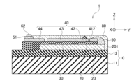
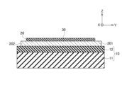
- FIG. 1 shows the configuration of a thermal print head according to Embodiment 1, and is a schematic cross-sectional view including a common electrode.
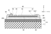
- FIG. 2 shows the configuration of the thermal print head according to the first embodiment, and is a schematic cross-sectional view including individual electrodes.
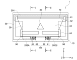
- FIG. 3 is a schematic plan view showing the configuration of the thermal print head according to the first embodiment.
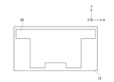
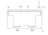
- FIG. 4 is a schematic plan view showing the arrangement of the conductor layer and the insulating layer of the thermal print head according to the first embodiment.
- FIG. 5 is a schematic plan view showing the arrangement of connection wiring of the thermal print head according to the first embodiment.
- FIG. 6 is a schematic plan view showing the wiring of the individual wiring section of the thermal print head according to the first embodiment.
- FIG. 7 is a schematic plan view showing the arrangement of the common electrode and individual electrodes of the thermal print head according to the first embodiment.
- FIG. 8 is a schematic diagram showing the configuration of a thermal printer according to the first embodiment.
- FIG. 9A is a schematic cross-sectional view (part 1) for explaining the method for manufacturing the thermal print head according to the first embodiment.
- FIG. 9B is a schematic plan view for explaining the method for manufacturing the thermal print head according to Embodiment 1 (Part 1).
- FIG. 10A is a schematic cross-sectional view for explaining the method for manufacturing the thermal print head according to Embodiment 1 (part 2).
- FIG. 10B is a schematic plan view for explaining the method for manufacturing the thermal print head according to the first embodiment (part 2).
- FIG. 11A is a schematic cross-sectional view for explaining the method for manufacturing the thermal print head according to the first embodiment (part 3).
- FIG. 11B is a schematic plan view for explaining the method for manufacturing the thermal print head according to the first embodiment (part 3).
- FIG. 12A is a schematic cross-sectional view for explaining the method for manufacturing the thermal print head according to Embodiment 1 (part 4).
- FIG. 12B is a schematic plan view for explaining the method for manufacturing the thermal print head according to Embodiment 1 (part 4).
- FIG. 13A is a schematic cross-sectional view for explaining the method for manufacturing the thermal print head according to Embodiment 1 (Part 5).
- FIG. 13B is a schematic plan view for explaining the method for manufacturing the thermal print head according to Embodiment 1 (Part 5).
- FIG. 14A is a schematic cross-sectional view for explaining the method for manufacturing the thermal print head according to Embodiment 1 (part 6).
- FIG. 14B is a schematic plan view for explaining the method for manufacturing the thermal print head according to Embodiment 1 (part 6).
- FIG. 15 is a schematic cross-sectional view showing the configuration of a thermal print head according to a modification of the first embodiment.
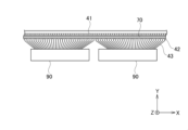
- FIG. 16 is a schematic cross-sectional view showing the positional relationship between the common electrode, individual electrodes, and heating resistors of the thermal print head according to the first embodiment.
- FIG. 17 is a schematic cross-sectional view showing the positional relationship between the common electrode, individual electrodes, and heating resistors of a thermal print head according to another embodiment.
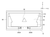
- FIG. 18 is a plan view showing a thermal print head according to the second embodiment.
- FIG. 19 is a sectional view taken along line II-II in FIG. 18.
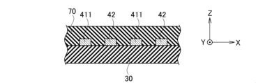
- FIG. 20 is a partially enlarged view taken along line III-III in FIG. 19.
- FIG. 21 is a plan view showing a thermal print head according to Embodiment 3.
- FIG. 22 is a plan view showing a thermal print head according to Embodiment 4.
- FIG. 23 is a plan view showing a thermal print head of a comparative example.
- the thermal print head 1 As shown in FIGS. 1 to 3, the thermal print head 1 according to the first embodiment includes a base 10, a conductor layer 20, an insulating layer 30, an electrode layer 40, a connection wiring 50, a common electrode terminal 61, and a control electrode terminal 62. , and a heating resistor 70.
- the electrode layer 40 includes a common electrode 41 , individual electrodes 42 , individual wiring sections 43 , control wiring sections 44 , and power supply wiring sections 45 .
- a plurality of heat generating resistors that generate heat due to the current flowing between the common electrode 41 and the individual electrodes 42 are provided in the heat generating resistor 70.
- the direction in which the common electrode 41 and the individual electrodes 42 are located when viewed from the base 10 is upward, and the base 10 is located when viewed from the common electrode 41 and the individual electrodes 42.
- the direction is downward.
- the surface facing upward is referred to as an upper surface
- the surface facing downward is referred to as a lower surface.
- the main scanning direction X is the direction in which the heating resistor 70 extends linearly.
- a plurality of heat generating resistor parts provided in the heat generating resistor 70 are arranged in the main scanning direction X.
- the sub-scanning direction Y is perpendicular to the main-scanning direction X and parallel to the upper surface of the base 10.
- the thickness direction Z is the normal direction of the upper surface of the base body 10. In other words, the thickness direction Z is a direction perpendicular to each of the main scanning direction X and the sub-scanning direction Y.
- FIG. 1 is a cross-sectional view along the II direction in FIG. 3 including the common electrode 41.
- FIG. 2 is a cross-sectional view along the II-II direction in FIG. 3 including the individual electrodes 42.
- FIG. 3 is a plan view of the base 10 viewed from the thickness direction.
- the conductive layer 20 and the insulating layer 30 are shown as broken lines that pass through the electrode layer 40 and the connection wiring 50.
- the protective film 80 shown in FIGS. 1 and 2 is not shown in FIG. 3.
- the control IC 90 shown in FIG. 3 is not shown in FIGS. 1 and 2.
- the base body 10 has a rectangular shape when viewed in plan from the thickness direction Z (hereinafter simply referred to as "plan view").
- the base 10 has a structure in which a substrate 11 and an underglaze layer 12 are laminated.
- a ceramic substrate or a single crystal semiconductor substrate may be used as the material for the substrate 11.
- an alumina substrate or the like can be used for the substrate 11, for example.
- a silicon substrate or the like can be used as the substrate 11, for example. From the viewpoint of heat dissipation, it is preferable to use an alumina substrate with relatively high thermal conductivity as the substrate 11.
- the underglaze layer 12 accumulates heat generated by the heating resistor 70. Therefore, the underglaze layer 12 is also called a heat storage layer.
- An insulating material can be used as the material for the underglaze layer 12.
- silicon dioxide which is the main component of glass, may be used for the underglaze layer 12.
- the size of the underglaze layer 12 in the thickness direction Z (hereinafter also simply referred to as "thickness") is not particularly limited, but is, for example, about 100 ⁇ m to 200 ⁇ m.
- the conductor layer 20 is arranged on the upper surface of the underglaze layer 12. Since the size of the unevenness on the upper surface of the substrate 11 made of a ceramic material or the like is reduced on the upper surface of the underglaze layer 12, the effect of flattening the upper surface of the base 10 on which the conductive layer 20 is arranged can also be obtained. .
- a conductive material such as metal may be used.
- silver (Ag) which is a relatively inexpensive and highly conductive material, is preferably used for the conductor layer 20.
- the thickness of the conductor layer 20 is, for example, about 3 ⁇ m to 20 ⁇ m.
- the conductor layer 20 has a first connection area 201 and a second connection area 202.
- the first connection region 201 is arranged on one side of the rectangular base 10, and the second connection region 202 is arranged on the side opposite to the side on which the first connection region 201 is arranged.
- the first connection region 201 is arranged close to the common electrode 41.
- the second connection region 202 is arranged close to the common electrode terminal 61.
- the thermal print head 1 has two regions as the second connection region 202: a second connection region 202A and a second connection region 202B. When the second connection area 202A and the second connection area 202B are not limited to each other, they are referred to as a second connection area 202.
- the insulating layer 30 is arranged on the upper surface of the conductor layer 20 with the first connection region 201 and the second connection region 202 of the conductor layer 20 exposed in plan view. In other words, as shown in FIG. 4, the remaining region of the conductor layer 20 excluding the first connection region 201 and the second connection region 202 is covered with the insulating layer 30 in plan view.
- a part of the outer edge of the conductor layer 20 is located outside the outer edge of the insulating layer 30 in plan view; Portions of the conductor layer 20 are a first connection region 201 and a second connection region 202. As shown in FIG.
- the outer edge of the insulating layer 30 is located outside the outer edge of the conductor layer 20 except for the first connection region 201 and the second connection region 202 of the conductor layer 20 .
- crystallized glass or the like may be used for the insulating layer 30.
- the thickness of the insulating layer 30 is, for example, about 10 ⁇ m to 30 ⁇ m.
- the electrode layer 40 is arranged on the upper surface of the insulating layer 30.
- the electrode layer 40 faces the conductor layer 20 with the insulating layer 30 in between.
- a heating resistor portion is provided between the common electrode 41 and the individual electrodes 42 in the heating resistor 70. Since the common electrode 41 and the individual electrodes 42 constitute a path for supplying electricity to the heating resistor 70, the material of the electrode layer 40 (hereinafter also referred to as "electrode material”) is a conductor.
- the electrode material for example, a metal material such as copper (Cu), silver, palladium (Pd), iridium (Ir), platinum (Pt), or gold (Au) may be used.
- the electrode material is preferably copper, silver, platinum, or gold.
- gold or the like is preferably used as the electrode material.
- the thickness of the electrode layer 40 is, for example, about 0.2 ⁇ m to 5 ⁇ m.
- the heating resistor 70 is arranged above the insulating layer 30 and is in contact with the common electrode 41 and the individual electrodes 42. Print dots are formed by the heating resistor portion of the heating resistor 70 generating heat due to the current flowing between the common electrode 41 and the individual electrodes 42 in the heating resistor 70 .
- a material having higher resistivity than the materials of the common electrode 41 and the individual electrodes 42 is used for the heating resistor 70.
- tantalum nitride, silicon dioxide containing tantalum, or the like may be used as the material of the heating resistor 70.
- ruthenium oxide may be used as the material for the heating resistor 70.
- the thickness of the heating resistor 70 is, for example, about 0.05 to 10 ⁇ m.
- connection wiring 50 is isolated from the individual electrodes 42 and is arranged above the underglaze layer 12 with an insulating layer 30 interposed between the conductor layer 20 except the first connection region 201 and the second connection region 202. There is. As shown in FIG. 3, the connection wiring 50 is arranged along the outer edge of the base 10. As shown in FIG.
- the first wiring region 501 of the connection wiring 50 covers the first connection region 201 of the conductor layer 20 and is electrically connected to the first connection region 201. Further, in the first wiring region 501, the connection wiring 50 overlaps a part of the common electrode 41 in a plan view. Thereby, the connection wiring 50 electrically connects the conductor layer 20 and the common electrode 41.
- the second wiring area 502A and the second wiring area 502B which are the ends of the connection wiring 50, cover at least a part of the second connection area 202 of the conductor layer 20 in plan view, and are electrically connected to the second connection area 202. Connecting. Specifically, the second wiring region 502A covers at least a portion of the second connection region 202A, and the second wiring region 502B covers at least a portion of the second connection region 202B.
- the second wiring area 502A and the second wiring area 502B are not limited to each other, they will be referred to as a second wiring area 502.
- the connection wiring 50 overlaps the common electrode terminal 61 in plan view. Thereby, the connection wiring 50 electrically connects the conductor layer 20 and the common electrode terminal 61.
- connection wiring 50 is connected to the first wiring area 501 connected to the first connection area 201 of the conductor layer 20 and the common electrode 41, and to the second connection area 202 of the conductor layer 20 and the common electrode terminal 61. It has a second wiring region 502 to which it is connected. Therefore, the common electrode 41 and the common electrode terminal 61 are electrically connected via the conductor layer 20 and the connection wiring 50.
- Silver which is relatively inexpensive and has good metallic properties and ionization tendency, is preferably used as the material for the connection wiring 50.
- a terminal group 60 in which a common electrode terminal 61 and a control electrode terminal 62 are arranged is arranged above the underglaze layer 12 in close proximity to the region where the second connection region 202 of the conductor layer 20 is arranged.
- an electric signal hereinafter referred to as "print" for setting the potential of the common electrode 41 and the individual electrodes 42 is sent to the common electrode terminal 61 and the control electrode terminal 62.
- the material for the terminal group 60 for example, silver (Ag)-platinum (Pt) material is suitably used.
- two terminals at each end of the terminal group 60 are common electrode terminals 61, and a plurality of control electrode terminals 62 are arranged between the common electrode terminals 61.
- Common electrode terminals 61 arranged at both ends of the terminal group 60 are connected to the second wiring region 502 of the connection wiring 50.
- the control electrode terminal 62 is electrically connected to a control IC 90 that sets the potential of the individual electrode 42.
- the control IC 90 is a semiconductor integrated circuit having a logic circuit for setting the potential of the individual electrode 42.
- the control wiring section 44 of the electrode layer 40 includes wiring that connects the control electrode terminal 62 and the control IC 90.
- the individual wiring section 43 of the electrode layer 40 includes wiring that electrically connects the control IC 90 and the individual electrode 42 .
- each of the individual electrodes 42 is individually connected to the control IC 90 by independent wiring of the individual wiring section 43.
- the first wiring region 501 of the connection wiring 50 and a part of the common electrode 41 overlap, and the first connection region 201 of the conductor layer 20 overlaps with the first wiring region 501. That is, the portion of the first wiring region 501 that overlaps the upper surface of the insulating layer 30 and a portion of the common electrode 41 overlap in plan view.
- the overlapping portion of the first wiring region 501 extends up the side surface of the insulating layer 30 above the first connection region 201 .
- the power supply wiring section 45 of the electrode layer 40 and the second wiring region 502 of the connection wiring 50 overlap. That is, the common electrode terminal 61 is arranged on the stacked structure of the electrode layer 40 and a portion of the second wiring region 502 that overlaps the upper surface of the insulating layer 30 . The overlapping portion of the second wiring region 502 extends up the side surface of the insulating layer 30 above the second connection region 202 .
- the thermal print head 1 As described above, in the thermal print head 1, conductive materials are laminated in the common electrode 41 and the common electrode terminal 61. Therefore, the electrical resistance between the common electrode 41 and the common electrode terminal 61 can be reduced.
- the thermal print head 1 further includes a protective film 80 that covers the heating resistor 70, the electrode layer 40, and the like.
- the protective film 80 protects the heating resistor 70 and the like from wear, corrosion, oxidation, and the like.
- the protective film 80 may be made of an insulating material such as amorphous glass.
- the thickness of the protective film 80 is, for example, about 2 ⁇ m to 10 ⁇ m. With the protective film 80 having a thickness within this range, it is possible to obtain a thermal print head 1 that can suppress poor pressure resistance and maintain good printing quality.
- the protective film 80 does not cover at least a portion of the upper surface of the terminal group 60. In other words, the common electrode terminal 61 and the control electrode terminal 62 are exposed outside the protective film 80.
- FIG. 7 shows an example of the thermal print head 1 in which the periphery of the heating resistor section 71 is enlarged.
- FIG. 7 is a plan view showing an example of the arrangement of the common electrode 41 and the individual electrodes 42 around the heating resistor section 71.
- the cross-sectional view along the II-II direction in FIG. 7 is included in the cross-sectional view in FIG. 1, and the cross-sectional view along the II-II direction in FIG. 7 is included in the cross-sectional view in FIG.
- the thermal print head 1 shown in FIG. 7 includes a comb-shaped common electrode 41, a plurality of comb teeth portions 411 of the common electrode 41, a plurality of individual electrodes 42 alternately arranged along the main scanning direction
- a heating resistor 70 is provided which is in contact with the tooth portion 411 and the individual electrode 42 .
- the heat generating resistor portion 71 is a region in the heat generating resistor 70 where a current flows between the comb teeth portion 411 and the individual electrodes 42 .
- Each of the comb teeth portions 411 extends in the sub-scanning direction Y from the common portion 412. Adjacent comb teeth portions 411 are arranged along the main scanning direction X at predetermined intervals. According to the thermal print head 1 having the comb-shaped common electrode 41, the interval between the comb teeth 411 and the individual electrodes 42 can be narrowed, and the pitch of the heating resistor parts 71 can be narrowed.
- the thermal print head 1 in which the pitch of the heating resistors 71 is narrow is capable of high-definition printing.
- the individual electrodes 42 are not electrically connected to each other. Therefore, when a thermal printer incorporating the thermal print head 1 is used, a potential can be set independently to each individual electrode 42. A potential of opposite polarity to the individual electrodes 42 is set on the common electrode 41 .
- the first connection region 201, the first wiring region 501, and the common portion 412 of the common electrode 41 extend in the main scanning direction X in parallel with the heating resistor 70.
- the common electrode 41 is arranged between the first connection region 201 and the first wiring region 501 and the heating resistor 70 in plan view.
- the common electrode 41 and the common electrode terminal 61 are electrically connected by both the conductor layer 20 and the connection wiring 50. Therefore, according to the thermal print head 1, compared to a thermal print head in which the common electrode 41 and the common electrode terminal 61 are connected only by wiring arranged above the insulating layer 30, the common electrode terminal 61 is connected to the common electrode terminal 61.
- the electrical resistance of wiring up to 41 can be reduced. As a result, it is possible to increase the power consumption of the heating resistor section 71 while suppressing an increase in the power consumption of the entire thermal print head 1. Therefore, according to the thermal print head 1, it is possible to suppress an increase in power consumption and improve printing efficiency.
- the outer edge of the common electrode 41 that overlaps the connection wiring 50 overlaps the outer edge of the insulating layer 30 in plan view. Then, along the outer edges of the common electrode 41 and the insulating layer 30, a current path is formed in the thickness direction Z by the first wiring region 501 that connects the conductor layer 20 and the common electrode 41. Therefore, a current path can be formed by the connection wiring 50 that connects the conductor layer 20 and the common electrode 41.
- the outer edge of the common electrode 41 overlapping the connection wiring 50 may be located inside the outer edge of the insulating layer 30.
- a print signal is transmitted from the outside of the thermal print head 1 to the control IC 90 via the control electrode terminal 62.
- the control IC 90 selectively sets the potential of the individual electrodes 42 in accordance with the print signal, so that the plurality of heat generating resistors 71 provided along the main scanning direction X in the heat generating resistor 70 selectively generate heat.
- the print medium such as thermal paper that is pressed against the heating resistor 70 is printed.
- the thermal printer shown in FIG. 8 has a platen roller 101 that directly faces the thermal print head 1.
- the thermal printer shown in FIG. 8 has a platen roller 101 that directly faces the thermal print head 1.
- the thermal printer shown in FIG. The print medium 100 is conveyed along the sub-scanning direction Y as shown by the arrow in FIG. Usually, the print medium 100 is conveyed from the terminal group 60 side toward the heating resistor 70 side. Print medium 100 is pressed against heat generating resistor 71 by platen roller 101 .
- the control IC 90 to which the printing signal has been transmitted sets any individual electrode 42 to a predetermined potential, and selectively activates any one of the plurality of heating resistors 71 provided in the heating resistor 70. develops a fever.
- the heat generated by the heat generating resistor section 71 is transferred to the print medium 100, whereby printing is performed on the print medium 100.
- the thermal printer may further include a measurement circuit, which is not shown.
- the measurement circuit measures the resistance value of each of the plurality of heat generating resistors 71.
- the measurement circuit measures the resistance value of the heat generating resistor section 71, for example, when printing is not performed on the print medium. By measuring the resistance value of the heat generating resistor section 71, the lifespan of the heat generating resistor section 71 can be estimated and the presence or absence of a malfunctioning heat generating resistor section 71 can be confirmed.
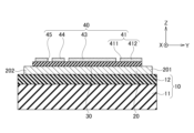
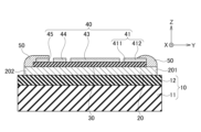
- FIGS. 9A, 9B to 14A, and 14B the drawings with A at the end are cross-sectional views taken along the II direction in FIG. 1, and the drawings with B at the end are plan views. It is.
- a base 10 in which a substrate 11 and an underglaze layer 12 are laminated is prepared.
- an underglaze layer 12 made of a glass material is formed on the upper surface of a substrate 11 made of a ceramic material.
- the underglaze layer 12 is formed at a firing temperature of, for example, about 1200°C.
- a conductor layer 20 is formed on the upper surface of the underglaze layer 12.
- a metal paste such as silver paste is applied by screen printing or the like, and the applied metal paste is fired to form the conductor layer 20.
- the conductor layer 20 may be formed into a predetermined shape using both screen printing and photolithography.
- the insulating layer 30 is formed on the upper surface of the conductor layer 20 so that the first connection region 201 and the second connection region 202 are exposed in plan view.
- crystallized glass or the like may be used as the material of the insulating layer 30.
- the insulating layer 30 and the conductive layer 20 may be formed so that a part of the outer edge of the conductive layer 20 is located outside the outer edge of the insulating layer 30 in plan view.
- the outer edge portions of the conductor layer 20 located outside the outer edge of the insulating layer 30 are the first connection region 201 and the second connection region 202 .
- an opening through which a part of the conductor layer 20 is exposed is formed in the insulating layer 30, and the first connection region 201 and the second connection region 202 are connected. It may be provided. However, by arranging the first connection region 201 and the second connection region 202 on the outside of the insulating layer 30, it is possible to form an opening in the insulating layer 30 that exposes the first connection region 201 and the second connection region 202. , the first connection region 201 and the second connection region 202 can be easily formed.
- the first connection region 201 is formed to extend in the main scanning direction X.
- an electrode layer 40 including a common electrode 41 and individual electrodes 42 is formed on the upper surface of the insulating layer 30.
- the electrode layer 40 is formed so that the common electrode 41 is close to the first connection region 201.
- a metal paste applied to the upper surface of the insulating layer 30 by screen printing or the like is fired.
- the common electrode 41, the individual electrodes 42, the individual wiring sections 43, the control wiring section 44, and the power supply wiring section 45 may be formed by patterning the metal paste using photolithography technology. For example, gold or the like may be used as the material of the electrode layer 40.
- the insulating layer 30 and the electrode layer 40 are arranged so that the outer edge of the common electrode 41 that overlaps with the connection wiring 50 overlaps with the outer edge of the insulating layer 30 or is located inside the outer edge of the insulating layer 30 in a plan view.
- the common portion 412 of the common electrode 41 is formed to extend in the main scanning direction X.
- connection wiring 50 is formed above 12.
- the connection wiring 50 is formed so that the first wiring area 501 is connected to the first connection area 201 and the common electrode 41, and the second wiring area 502 is connected to the second connection area 202.
- the connection wiring 50 may be formed using screen printing, photolithography, or the like. Silver is preferably used as the material for the connection wiring 50.
- connection wiring 50 is formed so as to overlap a part of the common electrode 41 in a plan view. That is, the connection wiring 50 is formed so that the portion of the first wiring region 501 that overlaps the upper surface of the insulating layer 30 and a part of the common electrode 41 overlap in plan view. For example, the first wiring region 501 overlaps the common portion 412 of the common electrode 41. Further, the connection wiring 50 is formed so that the portion of the second wiring region 502 that overlaps the upper surface of the insulating layer 30 and the power supply wiring section 45 overlap in plan view.
- a common electrode terminal 61 and a control electrode terminal 62 are formed.
- the common electrode terminal 61 is formed in the second wiring region 502 of the connection wiring 50 so as to be electrically connected to the common electrode 41 via the conductor layer 20 and the connection wiring 50.
- the common electrode terminal 61 is formed on the stacked structure of the portion of the connection wire 50 that overlaps the upper surface of the insulating layer 30 in the second wiring region 502 and the power supply wiring portion 45 of the electrode layer 40 .
- the control electrode terminal 62 is formed so as to be connected to the wiring of the control wiring section 44 connected to the control IC 90.
- the common electrode terminal 61 and the control electrode terminal 62 may be formed using screen printing, photolithography, or the like.
- a heating resistor 70 in contact with the common electrode 41 and the individual electrodes 42 is formed above the insulating layer 30.
- the heating resistor 70 may be formed using screen printing, photolithography, or the like.
- the heating resistor 70 extends in the main scanning direction X while intersecting the comb tooth portion 411 and the individual electrodes 42 in plan view.
- the control IC 90 is mounted at a predetermined position of the control wiring section 44, and the wiring of the individual wiring section 43 and the control wiring section 44 is connected to the control IC 90.
- the electrode layer 40 and the control IC 90 may be connected using solder.
- solder bumps are provided between the electrode layer 40 and the control IC 90, and the solder bumps are melted by heat treatment in an inert gas atmosphere such as nitrogen in a reflow oven, and the electrode layer 40 and the control IC 90 are electrically connected.
- a protective film 80 is formed above the insulating layer 30 so as to cover the heating resistor 70 and the electrode layer 40.
- the material of the protective film 80 may be glass.
- the protective film 80 does not cover at least a portion of the upper surfaces of the common electrode terminal 61 and the control electrode terminal 62.
- the material for the underglaze layer 12 is a material that has a higher firing temperature than the electrode layer 40, the connection wiring 50, the terminal group 60, and the heating resistor 70.
- the firing temperature of the underglaze layer 12 made of silicon dioxide, which is the main component of glass is about 1200°C
- the firing temperature of other conductive materials is about 810°C. Therefore, the manufacturing process including firing after forming the underglaze layer 12 can be simplified by performing it at a relatively low firing temperature.
- the common electrode 41 and the common electrode terminal 61 are electrically connected by both the conductor layer 20 and the connection wiring 50. Therefore, the electrical resistance of the wiring from the common electrode terminal 61 to the common electrode 41 can be reduced. As a result, it is possible to suppress an increase in the power consumption of the entire thermal print head 1 and to increase the power consumption in the heating resistor section 71. Therefore, according to the method for manufacturing the thermal print head 1 described above, it is possible to manufacture the thermal print head 1 that suppresses an increase in power consumption and improves printing efficiency.
- FIG. 15 shows a thermal print head 1A according to a modification of the first embodiment.
- a groove 200 that penetrates the conductor layer 20 in the thickness direction is provided in a region of the conductor layer 20 that overlaps the heating resistor 70 in a plan view.
- the groove 200 is surrounded by a conductor layer 20 .
- the groove 200 may be formed by, for example, photolithography and anisotropic etching. That is, a photoresist film or the like formed on the upper surface of the conductor layer 20 is patterned into a predetermined shape using photolithography technology to form an etching mask, and a part of the conductor layer 20 is selectively etched by anisotropic etching.
- the groove 200 may be formed by doing so.
- the underglaze layer 12 functions as a heat storage layer that stores heat generated by the heating resistor 70.
- the groove 200 that penetrates the conductor layer 20 in the thickness direction, the heat generated by the heating resistor 70 is easily transmitted to the underglaze layer 12. That is, according to the thermal print head 1A shown in FIG. 15, the deterioration of the heat storage function of the underglaze layer 12 can be suppressed.
- FIG. 15 shows an example in which the groove 200 is filled with the insulating layer 30, the inside of the groove 200 may be a space, or the inside of the groove 200 may be filled with a material having good thermal conductivity. Further, the groove 200 may be formed in the entire area below the heat generating resistor 70, or may be formed in a portion below the heat generating resistor 70.
- a heat generating resistor 70 may be disposed between the comb teeth 411, the individual electrodes 42, and the insulating layer 30.
- the heat generating resistor 71 generates heat in the heat generating resistor 70 due to the current flowing between the comb teeth portion 411 of the common electrode 41 and the individual electrodes 42 .
- Embodiment 1 includes various embodiments not described here.
- Embodiment 2 18 to 20 show a thermal print head according to Embodiment 2 of the present disclosure.
- the thermal print head 1B is installed in a printer that prints on a print medium 8 that is conveyed while being sandwiched between a platen roller (not shown).
- print media 8 include thermal paper for creating barcode sheets, receipts, and the like.
- FIG. 18 is a plan view showing a thermal print head 1B according to the second embodiment.
- the thermal print head 1B includes a substrate 11A, a heat generating resistor 4, a plurality of individual electrodes 32, a plurality of common electrodes 31, an auxiliary electrode 35, a common ground electrode 14, a plurality of drive ICs 5, and a first wiring. It includes a group 21 , a second wiring group 22 , an external terminal 9 , and a joining member 16 .
- the substrate 11A has a rectangular flat plate shape in plan view, and is made of, for example, alumina ceramic.
- the main scanning direction X shown in FIG. 18 is the longitudinal direction of the substrate 11A, and the sub-scanning direction Y is the lateral direction of the substrate 11A.
- the thickness direction Z shown in FIGS. 19 and 20 is the thickness direction of the substrate 11A.
- the thickness of the substrate 11A is, for example, 1 mm.
- the heat generating resistor section 4 is a heat generating source of the thermal print head 1B.
- the heat generating resistor section 4 has a band-like shape extending in the main scanning direction X, and is sandwiched between a plurality of individual electrodes 32 and a plurality of common electrodes 31.
- the heating resistor section 4 generates heat by creating a potential difference between the plurality of individual electrodes 32 and the plurality of common electrodes 31. Note that the plurality of individual electrodes 32 and the plurality of common electrodes 31 have a large number of wires spaced apart from each other, but are shown in black in the figure.
- the plurality of individual electrodes 32 are arranged side by side with gaps in the main scanning direction X.
- the plurality of individual electrodes 32 are electrically connected to the plurality of drive ICs, and are arranged in a bundle corresponding to each drive IC 5.
- the plurality of individual electrodes 32 are arranged at regular intervals along the main scanning direction X, like comb teeth, with gaps between them.
- Each of the plurality of individual electrodes 32 extends toward the heat generating resistor section 4 in the sub-scanning direction Y so as to expand from the drive IC 5.
- the plurality of common electrodes 31 are arranged between each of the plurality of individual electrodes 32.
- the plurality of common electrodes 31 are arranged on the side opposite to the plurality of drive ICs 5 with respect to the heating resistor section 4 .
- the plurality of common electrodes 31 are arranged like comb teeth at equal intervals along the main scanning direction X with gaps.
- Each of the plurality of common electrodes 31 is arranged to alternate with each of the plurality of individual electrodes 32 adjacent to each other in the main scanning direction X.
- the plurality of common electrodes 31 have root portions connected in a band shape.
- the auxiliary electrode 35 is provided so as to cover the root portions of the plurality of common electrodes 31.
- the auxiliary electrode 35 can be preferably made of silver, for example, and is provided to reduce electrical resistance.
- the plurality of drive ICs 5 perform drive control to partially generate heat in the heat generating resistor section 4 by supplying current to the heat generating resistor section 4 via the plurality of individual electrodes 32 and the plurality of common electrodes 31.
- the plurality of drive ICs 5 selectively energize the plurality of individual electrodes 32 based on a control signal received from an external device, thereby generating heat at an arbitrary position of the heating resistor section 4.
- the plurality of drive ICs 5 are covered with sealing resin (not shown) for protection.
- the plurality of drive ICs 5 include a first group of drive ICs 111 and a second group of drive ICs 112.
- the external terminal 9 includes a first external terminal 9X and a second external terminal 9Y.
- the first group of drive ICs 111 and the first external terminals 9X are electrically connected via the first wiring group 21.
- the second group of drive ICs 112 and the second external terminals 9Y are electrically connected via the second wiring group 22.
- the plurality of drive ICs 5 are divided into two systems, a first group of drive ICs 111 and a second group of drive ICs 112, due to design requirements such as securing space for parts (such as thermistors) placed in the header and routing of wiring. It is divided. Note that the plurality of drive ICs 5 may be divided into three or more systems. The systems indicate that they are of the same type, and for example, the wiring groups are different for each system, but the drive control in the plurality of drive ICs 5 is the same.
- the first wiring group 21 and the second wiring group 22 are composed of a collection of multiple wirings. In the drawing, illustration of wiring is omitted.
- the first wiring group 21 includes a plurality of power supply electrodes 21a, a first ground electrode 21b, and a plurality of signal electrodes 21c.
- the second wiring group 22 includes a plurality of power supply electrodes 22a, a second ground electrode 22b, and a plurality of signal electrodes 22c.
- the power supply electrode 21a is an electrode for supplying power to each of the first group of drive ICs 111 among the plurality of drive ICs 5.
- the first ground electrode 21b is an electrode for supplying a ground potential to each of the first group of drive ICs 111 among the plurality of drive ICs 5.
- the signal electrode 21c is an electrode for supplying a signal to each of the first group of drive ICs 111 among the plurality of drive ICs 5.
- the power supply electrode 22a is an electrode for supplying power to each of the second group of drive ICs 112 among the plurality of drive ICs 5.
- the second ground electrode 22b is an electrode for supplying a ground potential to each of the second group of drive ICs 112 among the plurality of drive ICs 5.
- the signal electrode 22c is an electrode for supplying a signal to each of the second group of drive ICs 112 among the plurality of drive ICs 5.
- the common ground electrode 14 is provided above the first ground electrode 21b and the second ground electrode 22b in the thickness direction Z in the thermal print head 1B.
- the common ground electrode 14 is electrically connected to the first ground electrode 21b and the second ground electrode 22b via the joining member 16.
- the joining member 16 is made of a conductive member.
- the first external terminal 9X includes a power terminal 90A for connecting to the plurality of power supply electrodes 21a, a ground terminal 91 for connecting to the first ground electrode 21b, and a ground terminal 92 for connecting to the common ground electrode 14. , and a signal terminal 93 for connecting to the plurality of signal electrodes 21c.
- the second external terminal 9Y includes a power terminal 90A for connecting to the plurality of power supply electrodes 22a, a grounding terminal 91 for connecting to the second grounding electrode 22b, and a grounding terminal 92 for connecting to the common grounding electrode 14. , and a signal terminal 93 for connecting to the plurality of signal electrodes 22c.
- a joining member 16 is arranged on each of the external terminals 9 to adjust the thickness in the thickness direction Z. Note that the bonding members 16 for adjusting the thickness may be disposed not on all the external terminals 9 but only on some of the external terminals 9.
- the electrodes, wiring, terminals, and bonding member 16 in this embodiment may be made of a member containing metal particles such as copper, silver, platinum, and gold.
- FIG. 23 is a plan view showing a thermal print head 1E of a comparative example.
- a plurality of drive ICs 5 are used to drive the first group due to design requirements such as ensuring space for parts (for example, thermistors, etc.) placed in the header and routing wiring. It may be divided into two systems: the IC 111 and the second group of drive ICs 112.
- a plurality of individual electrodes 32 are connected to one side of the plurality of drive ICs 5, in contact with the heating resistor portion 4 arranged in the longitudinal direction of the substrate 11A, and arranged in the transverse direction of the substrate 11A.
- a plurality of common electrodes 31 electrically connected to the plurality of individual electrodes 32 are provided on the opposite side of the plurality of individual electrodes 32 via the heating resistor section 4 .
- the first wiring group 21 includes a plurality of power supply electrodes 21a that supply power to each of the plurality of drive ICs 5, a first ground electrode 21b that supplies a ground potential to each of the plurality of drive ICs, and a plurality of first ground electrodes 21b that supply a ground potential to each of the plurality of drive ICs.
- a plurality of signal electrodes 21c that supply signals to each of the drive ICs are included.
- the second wiring group 22 includes a plurality of power supply electrodes 22a that supply power to each of the plurality of drive ICs 5, a second ground electrode 22b that supplies a ground potential to each of the plurality of drive ICs 5, and a plurality of second ground electrodes 22b that supply a ground potential to each of the plurality of drive ICs 5.
- a plurality of signal electrodes 22c are included for supplying signals to each of the drive ICs.
- the external terminal 9 includes a first external terminal 9X and a second external terminal 9Y.
- the first external terminal 9X includes a power terminal 90A for connecting to the plurality of power supply electrodes 21a, a grounding terminal 91C for connecting to the first grounding electrode 21b, and a signal terminal 93 for connecting to the plurality of signal electrodes 21c.
- the second external terminal 9Y includes a power terminal 90A for connecting to the plurality of power supply electrodes 22a, a grounding terminal 91C for connecting to the second grounding electrode 22b, and a signal terminal 93 for connecting to the plurality of signal electrodes 22c. including.
- the first ground electrode 21b of the first group of drive ICs 111 and the second ground electrode 22b of the second group of drive ICs 112 are provided with separate ground electrodes and are not electrically connected. do not have. Therefore, a difference in voltage drop may occur between the first ground electrode 21b of the first group of drive ICs 111 and the second ground electrode 22b of the second group of drive ICs 112. This causes a difference in power consumption between the heat generating resistor section 4 corresponding to the first group of drive ICs 111 and the heat generating resistor section 4 corresponding to the second group of drive ICs 112, resulting in a difference in print density. Appropriate printing may not be possible.
- thermal print head 1B of Embodiment 2 it is possible to solve the problem that a difference occurs in printing density and it is not possible to perform suitable printing as in the thermal print head 1E of the comparative example.
- FIG. 19 is a sectional view taken along line II-II in FIG. 18.
- FIG. 20 is a partially enlarged view taken along line III-III in FIG. 19.
- a heating resistor 4 is provided at the end of the thermal print head 1B in the sub-scanning direction Y, and a heating resistor 4 is provided at the center position of the thermal print head 1B in the sub-scanning direction Y, where a plurality of drive ICs 5 are arranged.
- a joining member 16 is arranged.
- the part where the heating resistor section 4 is provided will be explained.
- a glaze layer 2 an electrode layer 3, a heating resistor 4, and a protective layer 7 are laminated in order from the substrate 11A.
- the glaze layer 2 is made of glass and is formed to cover the surface of the substrate 11A.
- the glaze layer 2 is for providing a smooth surface suitable for installing the electrode layer 3, the heating resistor 4, and the plurality of drive ICs 5.
- a part of the surface of the glaze layer 2 bulges in the thickness direction Z. This bulging portion is referred to as a bulging portion 23.
- the electrode layer 3 includes a plurality of individual electrodes 32 and a plurality of common electrodes 31. The ends of the plurality of common electrodes 31 are electrically connected to the auxiliary electrode 35.
- the heat generating resistor section 4 is arranged above the bulge section 23 with the electrode layer 3 interposed therebetween.
- the protective layer 7 covers the electrodes and the heat generating resistor 4 to protect the electrodes and the heat generating resistor 4 from foreign substances and the like.
- the protective layer 7 is formed of a suitable material selected from glass, sialon, tantalum nitride, and silicon carbide, for example.
- the cross section of the position where the plurality of drive ICs 5 are arranged in the sub-scanning direction Y includes, in order from the substrate 11A, the glaze layer 2, the first wiring group 21, the insulating layer 6, the bonding member 16, A common ground electrode 14 and a protective layer 7 are laminated.
- the first ground electrode 21b included in the first wiring group 21 is electrically connected to the common ground electrode 14 via the joining member 16.
- the insulating layer 6 is formed of a non-conductive material to prevent electrical connection between the upper layer and the lower layer at positions other than the bonding member 16. Note that the stacking relationship between the second ground electrode 22b included in the second wiring group 22 and the common ground electrode 14 is also the same as the stacking relationship in FIGS. 19 and 20.
- the first ground electrode 21b included in the first wiring group 21 and the second ground electrode 22b included in the second wiring group 22 include a plurality of individual electrodes 32 and a plurality of common electrodes 31. , are arranged on the electrode layer 3 as the first electrode layer of the substrate 11A on which the plurality of power supply electrodes 21a, 22a and the plurality of signal electrodes 21c, 22c are provided.
- the common ground electrode 14 is arranged on the second electrode layer laminated on the electrode layer 3 with the insulating layer 6 interposed therebetween. Therefore, the common ground electrode 14 can be freely arranged without considering the arrangement of the first wiring group 21 and the second wiring group 22 provided in the first electrode layer.
- the common ground electrode 14 is connected to the second electrode layer so as to surround each of the drive ICs 111 of the first group and each of the drive ICs 112 of the second group.
- the first ground electrode 21b and the second ground electrode 22b can be simply connected by wiring.
- Wiring resistance can be reduced compared to the case where Note that the first ground electrode 21b, the second ground electrode 22b, and the common ground electrode 14 are electrically connected to each other via the bonding member 16 at both ends of each of the first group of drive ICs 111 and the second group of drive ICs 112. is joined to.
- the thermal print head 1B According to the thermal print head 1B, the first ground electrode 21b, the second ground electrode 22b, and the common ground electrode 14 are bonded at both ends of each of the first group of drive ICs 111 and the second group of drive ICs 112. They are electrically connected via 16. Therefore, the thermal print head 1B can reduce the difference between the voltage drop amount at the first ground electrode 21b and the voltage drop amount at the second ground electrode 22b via the common ground electrode 14. As a result, the thermal print head 1B can equalize power consumption between the heat generating resistor section 4 driven by the first group driving IC 111 and the heat generating resistor section 4 driven by the second group driving IC 112. It is possible to prevent differences in density from occurring and perform suitable printing.
- the thermal print head 1B has the common ground electrode 14 arranged on the second electrode layer above the first electrode layer. Therefore, in the thermal print head 1B, the wiring widths of the plurality of power supply electrodes 21a and signal electrodes 21c included in the first wiring group 21 and the power supply electrodes 22a and signal electrodes 22c included in the second wiring group 22 are connected to a common ground. A wider area can be secured than when the electrode 14 is provided in the first electrode layer. Thereby, the wiring resistance of the first electrode layer can be reduced, and the power loss in the first wiring group 21 and the second wiring group 22 can be reduced.
- the thermal print head 1B since the thermal print head 1B has the common ground electrode 14 wired in the second electrode layer where no other wires are provided, the wire width of the common ground electrode 14 can be controlled without being restricted by other wires. A wide area can be secured, and wiring resistance can be reduced.
- the bonding member 16 is also arranged at the position of the external terminal 9. Thereby, unevenness is not generated in the thickness direction Z, and the thickness can be made uniform.
- the thermal print head 1B has a configuration in which the distance from the external terminal 9 to the plurality of drive ICs 5 is shorter than the distance from the plurality of drive ICs 5 to the heat generating resistor section 4 in the lateral direction of the thermal print head 1B. Thereby, the wiring resistance from the external terminal 9 for connection with external equipment to the plurality of drive ICs 5 can be reduced.
- FIG. 21 is a plan view showing a thermal print head 1C according to the third embodiment. Note that in FIG. 21, the same components as those described in Embodiment 2 are denoted by the same reference numerals, and detailed description thereof will be omitted.
- the common ground electrode 14A is connected and arranged to surround the first group of drive ICs 111 and the second group of drive ICs 112 in the second electrode layer.
- the first ground electrode 21b, the second ground electrode 22b, and the common ground electrode 14A are electrically connected via the joining member 16 at both ends of the first group of drive ICs 111 and the second group of drive ICs 112.
- the thermal print head 1C According to the thermal print head 1C, the first ground electrode 21b, the second ground electrode 22b, and the common ground electrode 14 are connected via the joining member 16 at both ends of the first group drive IC 111 and the second group drive IC 112. electrically connected. Therefore, the thermal print head 1C can reduce the difference between the voltage drop amount at the first ground electrode 21b and the voltage drop amount at the second ground electrode 22b via the common ground electrode 14. As a result, the thermal print head 1C can equalize power consumption between the heat generating resistor section 4 driven by the first group driving IC 111 and the heat generating resistor section 4 driven by the second group driving IC 112. It is possible to prevent differences in density from occurring and perform suitable printing.
- the thermal print head 1C has the common ground electrode 14 arranged on the second electrode layer above the first electrode layer. For this reason, the thermal print head 1C has a common grounding with respect to the wiring widths of the plurality of power supply electrodes 21a and signal electrodes 21c included in the first wiring group 21 and the wiring widths of the power supply electrodes 22a and signal electrodes 22c included in the second wiring group 22. A wider area can be secured than when the electrode 14 is provided in the first electrode layer. Thereby, the wiring resistance of the first electrode layer can be reduced, and the power loss in the first wiring group 21 and the second wiring group 22 can be reduced.
- the thermal print head 1C has the common ground electrode 14 wired in the second electrode layer where no other wires are provided, the wire width of the common ground electrode 14 can be controlled without being restricted by other wires. A wide area can be secured, and wiring resistance can be reduced.
- FIG. 22 is a plan view showing a thermal print head 1D according to the third embodiment. Note that in FIG. 22, the same components as those described in Embodiment 2 are denoted by the same reference numerals, and detailed description thereof will be omitted.
- the common ground electrode 14B is connected and arranged so as to surround the plurality of drive ICs 5 in the second electrode layer.
- the first ground electrode 21b, the second ground electrode 22b, and the common ground electrode 14B are electrically connected via the joining member 16 at both ends of the plurality of drive ICs 5.
- the thermal print head 1D According to the thermal print head 1D, the first ground electrode 21b, the second ground electrode 22b, and the common ground electrode 14 are electrically joined via the joining member 16 at both ends of the plurality of drive ICs 5. Therefore, the thermal print head 1D can reduce the difference between the voltage drop amount at the first ground electrode 21b and the voltage drop amount at the second ground electrode 22b via the common ground electrode 14. Thereby, the thermal print head 1D can equalize power consumption between the heat generating resistor section 4 driven by the first group drive IC 111 and the heat generating resistor section 4 driven by the second group drive IC 112, and print It is possible to prevent differences in density from occurring and perform suitable printing.
- the thermal print head 1D has the common ground electrode 14 arranged on the second electrode layer above the first electrode layer. For this reason, the thermal print head 1D has a common grounding with respect to the wiring widths of the plurality of power supply electrodes 21a and signal electrodes 21c included in the first wiring group 21 and the wiring widths of the power supply electrodes 22a and signal electrodes 22c included in the second wiring group 22. A wider area can be secured than when the electrode 14 is provided in the first electrode layer. Thereby, the wiring resistance of the first electrode layer can be reduced, and the power loss in the first wiring group 21 and the second wiring group 22 can be reduced.
- the common ground electrode 14 is wired in the second electrode layer where no other wires are provided, the wire width of the common ground electrode 14 can be controlled without being restricted by other wires. A wide area can be secured, and wiring resistance can be reduced.
- the bonding member 16 is disposed below each of the portions of the common ground electrode 14 that extend in the sub-scanning direction Y.
- the joining members 16 may not be arranged at all positions of the portion.
- the first ground electrode 21b and the second ground electrode 22b may be electrically bonded to each other at at least one location among the plurality of portions of the common ground electrode 14 extending in the sub-scanning direction Y.
- Embodiments 2 to 4 include various embodiments not described here.
- the configuration may be a combination of Embodiment 1 and Embodiments 2 to 4 as appropriate.
- the first ground electrode 21b, the second ground electrode 22b, and the common ground electrode 14 are connected to the first group of drive ICs 111.
- a configuration may also be adopted in which the driving ICs 112 and the second group of drive ICs 112 are electrically connected to each other via the joining member 16 at both ends. With such a configuration, it is possible to suppress an increase in power consumption, improve printing efficiency, and furthermore, it is possible to prevent differences in printing density from occurring.
- the present disclosure includes configurations related to the following additional notes.
- an underglaze layer 12 (Additional note 1) an underglaze layer 12; a conductor layer 20 disposed on the top surface of the underglaze layer 12;
- the insulating layer 30 disposed on the upper surface of the conductor layer 20 is exposed with the first connection region 201 and the second connection region 202 of the conductor layer 20 exposed in a plan view from the thickness direction of the underglaze layer 12.
- connection wiring 50 having a first wiring area 501 connected to the first wiring area 501 and a second wiring area 502 connected to the second connection area 202; a common electrode terminal 61 arranged in the second wiring region 502 of the connection wiring 50;
- a thermal print head 1, 1A comprising: a heating resistor 70 disposed above an insulating layer 30 and in contact with a common electrode 41 and an individual electrode 42.
- the common electrode 41 and the common electrode terminal 61 are electrically connected by both the conductor layer 20 and the connection wiring 50. Therefore, according to the thermal print heads 1 and 1A described in Appendix 1, the electrical resistance between the common electrode 41 and the common electrode terminal 61 can be reduced. As a result, it is possible to suppress an increase in the overall power consumption of the thermal print heads 1 and 1A, and to increase the heat generated by the heat generating resistor section. Therefore, according to the thermal print heads 1 and 1A described in Appendix 1, it is possible to suppress an increase in power consumption and improve printing efficiency.
- thermo print head 1, 1A according to appendix 1, wherein the portion of the first wiring region 501 that overlaps the upper surface of the insulating layer 30 and a part of the common electrode 41 overlap in plan view.
- conductive materials are laminated in the common electrode 41 and the common electrode terminal 61. Therefore, the electrical resistance between the common electrode 41 and the common electrode terminal 61 can be reduced.
- the thermal print head 1A described in Appendix 4 by providing the groove 200 penetrating the conductor layer 20 in the thickness direction, the heat generated by the heating resistor 70 is transferred to the underglaze layer 12 which is a heat storage layer. It becomes easier to convey the message.
- the manufacturing process including firing after forming the underglaze layer 12 can be simplified by performing it at a relatively low firing temperature.
- a current path can be formed by the connection wiring 50 that connects the conductor layer 20 and the common electrode 41.
- connection wiring 50 can be obtained at low cost and having good metal properties and ionization tendency.
- the common electrode 41 and the common electrode terminal 61 are electrically connected by both the conductor layer 20 and the connection wiring 50. Therefore, according to the thermal printer described in Appendix 10, the electrical resistance between the common electrode 41 and the common electrode terminal 61 can be reduced. As a result, it is possible to suppress an increase in the overall power consumption of the thermal printer and to increase the heat generated by the heat generating resistor. Therefore, according to the thermal printer described in Appendix 10, it is possible to suppress an increase in power consumption and improve printing efficiency.
- the common electrode 41 and the common electrode terminal 61 are electrically connected by both the conductor layer 20 and the connection wiring 50. Therefore, according to the method for manufacturing the thermal print heads 1 and 1A described in Appendix 11, the electrical resistance between the common electrode 41 and the common electrode terminal 61 can be reduced. As a result, it is possible to suppress an increase in the overall power consumption of the thermal print heads 1 and 1A, and to increase the heat generated by the heat generating resistor section. Therefore, according to the method for manufacturing the thermal print head 1, 1A described in Appendix 11, it is possible to manufacture the thermal print head 1, 1A that suppresses an increase in power consumption and improves printing efficiency.
- connection wiring 50 is formed so that the portion of the first wiring region 501 that overlaps the upper surface of the insulating layer 30 and a part of the common electrode 41 overlap in plan view; 1A manufacturing method.
- the common electrode terminal 61 is formed on a laminated structure of the electrode layer 40 and a portion of the second wiring region 502 that overlaps the upper surface of the insulating layer 30. Production method.
- conductive materials are laminated on the common electrode 41 and the common electrode terminal 61. Therefore, the electrical resistance between the common electrode 41 and the common electrode terminal 61 can be reduced.
- the heat generated by the heat generating resistor 70 is transferred to the underlayer which is the heat storage layer. This becomes easier to transmit to the glaze layer 12.
- the manufacturing process including firing after forming the underglaze layer 12 can be simplified by performing it at a relatively low firing temperature.
- a current path can be formed by the connection wiring 50 that connects the conductor layer 20 and the common electrode 41.
- the insulating layer 30 and the conductive layer 20 are formed such that a part of the outer edge of the conductor layer 20 is located outside the outer edge of the insulating layer 30 in a plan view, and a part is connected to the first connection region 201 and the first connection region 201. 2 connection area 202.
- connection wiring 50 can be formed at low cost and having good metal properties and ionization tendency.
- Thermal print heads 1B, 1C, and 1D include a substrate 11A, a heat generating resistor section 4 arranged in the longitudinal direction of the substrate 11A, and a plurality of individual electrodes in contact with the heat generating resistor section 4 and arranged in the transverse direction of the substrate 11A.
- 32 is electrically connected to a plurality of individual electrodes 32 via the heating resistor 4, and is electrically connected to a plurality of common electrodes 31 arranged in the transverse direction of the substrate 11A and a plurality of individual electrodes 32.
- a plurality of power supply electrodes 21a, 22a supplying power to each of the plurality of drive ICs 5, a plurality of signal electrodes 21c, 22c supplying signals to each of the plurality of drive ICs 5, a ground electrode, a plurality of power supply electrodes 21a, 22a, and a plurality of signal electrodes. It includes an external terminal 9 electrically connected to the electrodes 21c and 22c.
- External terminal 9 includes a first external terminal 9X and a second external terminal 9Y.
- the plurality of drive ICs 5 include a first group of drive ICs 111 electrically connected to the first external terminal 9X, and a second group of drive ICs 112 electrically connected to the second external terminal 9Y.
- the ground electrodes include a first ground electrode 21b electrically connected to each of the drive ICs 111 of the first group, a second ground electrode 22b electrically connected to each of the drive ICs 112 of the second group, and a first ground electrode 22b electrically connected to each of the drive ICs 112 of the second group. It includes a common ground electrode 14 that electrically connects the ground electrode 21b and the second ground electrode 22b.
- the first ground electrode 21b and the second ground electrode 22b are arranged on the first electrode layer of the substrate 11A on which the plurality of individual electrodes 32 and the plurality of power supply electrodes 21a and 22a are provided.
- the common ground electrode 14 is connected to a second electrode layer laminated on the first electrode layer with the insulating layer 6 interposed therebetween so as to surround the plurality of drive ICs 5 .
- the first ground electrode 21b, the second ground electrode 22b, and the common ground electrode 14 are electrically connected via the joining member 16 at both ends of the plurality of drive ICs 5.
- the common ground electrode 14 is connected to the second electrode layer so as to surround the first group of drive ICs 111 and the second group of drive ICs 112. be done.
- the first ground electrode 21b, the second ground electrode 22b, and the common ground electrode 14 are electrically connected via the joining member 16 at both ends of the first group of drive ICs 111 and the second group of drive ICs 112.
- the common ground electrode 14 is provided in the second electrode layer so as to surround each of the drive ICs 111 of the first group and each of the drive ICs 112 of the second group. arranged in a connected manner.
- the first ground electrode 21b, the second ground electrode 22b, and the common ground electrode 14 are electrically connected via the joining member 16 at both ends of each of the first group of drive ICs 111 and the second group of drive ICs 112. be done.
- (Appendix A5) The thermal print head 1B, 1C, or 1D according to any one of (Appendix A1) to (Appendix A4), in which the thermal print head 1B, 1C, or 1D is connected from the external terminal 9 to the plurality of drive ICs 5 in the short direction of the thermal print head 1B, 1C, or 1D.
- the distance is shorter than the distance from the plurality of drive ICs 5 to the heat generating resistor section 4.
- thermal print heads 1B, 1C, and 1D of the present disclosure power consumption can be made uniform between the heat generating resistor section 4 driven by the first group driving IC 111 and the heat generating resistor section 4 driven by the second group driving IC 112. It is possible to prevent differences in print density from occurring, and to perform suitable printing.
Landscapes
- Electronic Switches (AREA)
Abstract
サーマルプリントヘッドは、アンダーグレーズ層と、アンダーグレーズ層の上面に配置された導電体層と、導電体層の第1接続領域と第2接続領域が露出した状態で導電体層の上面に配置された絶縁層と、絶縁層の上面に配置され、共通電極と個別電極とを含む電極層と、第1接続領域と共通電極に接続している第1配線領域および第2接続領域に接続している第2配線領域を有する接続配線と、接続配線の第2配線領域に配置された共通電極端子と、共通電極および個別電極に接している発熱抵抗体を備える。
Description
本実施形態は、サーマルプリントヘッド、サーマルプリンタおよびサーマルプリントヘッドの製造方法に関する。
サーマルプリントヘッド(単に、サーマルヘッドとも称する)を用いた印刷は、主走査方向に並ぶ複数の発熱抵抗部(発熱部とも称する)を選択的に発熱させ、発熱抵抗部の熱を印刷媒体に伝導させることにより行われる。発熱抵抗部は、蓄熱層とも称されるグレーズ層の上に配置した発熱抵抗体の、共通電極と個別電極の間を流れる電流により発熱する領域である。印刷媒体は、バーコードシート又はレシートを作成するための感熱紙などである。
サーマルプリントヘッドを用いた印刷について、印字効率の向上が望まれている。発熱抵抗部で発生する熱を増大させることにより、印字効率の向上を実現できる。しかしながら、発熱抵抗部で発生する熱を増大させるためにサーマルプリントヘッドの電力が増大することは、サーマルプリントヘッドの省電力化に逆行する。
また、従来のサーマルプリントヘッドは、接地電位を供給するための電極の配置により発熱抵抗部において消費電力の差が生じることがある。これにより、従来のサーマルプリントヘッドでは、発熱抵抗部において印刷濃度に差が生じ、好適な印刷ができないことがあった。
本開示は、印字効率を向上し、かつ消費電力の増大を抑制できるサーマルプリントヘッド、サーマルプリンタおよびサーマルプリントヘッドの製造方法を提供することを目的とする。
また、本開示は、印刷濃度の差が低減された好適な印刷が可能なサーマルプリントヘッドを提供することを目的とする。
本開示の一態様は、アンダーグレーズ層と、アンダーグレーズ層の上面に配置された導電体層と、アンダーグレーズ層の厚さ方向から見た平面視において導電体層の第1接続領域と第2接続領域が露出した状態で導電体層の上面に配置された絶縁層と、絶縁層の上面に配置され、共通電極と個別電極を含む電極層と、個別電極から隔離し、かつ第1接続領域および第2接続領域を除いた導電体層とは絶縁層を介して対向し、第1接続領域と共通電極に接続している第1配線領域および第2接続領域に接続している第2配線領域を有する接続配線と、接続配線の第2配線領域に配置された共通電極端子と、絶縁層の上方に配置され、共通電極および個別電極に接している発熱抵抗体を備えるサーマルプリントヘッドである。
本開示の他の態様は、上記サーマルプリントヘッドを備えるサーマルプリンタである。
本開示の更に他の態様は、アンダーグレーズ層の上面に導電体層を形成し、アンダーグレーズ層の厚さ方向から見た平面視において導電体層の第1接続領域と第2接続領域が露出した状態で導電体層の上面に絶縁層を形成し、共通電極と個別電極を含む電極層を絶縁層の上面に形成し、第1接続領域と共通電極に接続する第1配線領域および第2接続領域に接続する第2配線領域を有する接続配線を、個別電極から隔離し、かつ第1接続領域および第2接続領域を除いた導電体層とは絶縁層を介して対向するように形成し、接続配線の第2配線領域に共通電極端子を形成し、共通電極および個別電極に接する発熱抵抗体を絶縁層の上方に形成する、サーマルプリントヘッドの製造方法である。
本開示の更に他の態様は、矩形状のサーマルプリントヘッドであって、基板と、基板の長手方向に配置される発熱抵抗部と、発熱抵抗部と接し、基板の短手方向に配置される複数の個別電極と、発熱抵抗部を介して複数の個別電極と電気的に接続し、基板の短手方向に配置される複数の共通電極と、複数の個別電極と電気的に接続し、サーマルプリントヘッドの長手方向に並んで配置される複数の駆動ICと、複数の駆動ICの各々に対して接地電位を供給する接地電極と、複数の駆動ICの各々に対して電源を供給する複数の電源電極と、複数の駆動ICの各々に対して信号を供給する複数の信号電極と、接地電極、複数の電源電極および複数の信号電極と電気的に接続する外部端子と、を備える。外部端子は、第1外部端子と、第2外部端子とを含む。複数の駆動ICは、第1外部端子と電気的に接続される第1群の駆動ICと、第2外部端子と電気的に接続される第2群の駆動ICとを含む。接地電極は、第1群の駆動ICの各々と電気的に接続される第1接地電極と、第2群の駆動ICの各々と電気的に接続される第2接地電極と、第1接地電極と第2接地電極とを電気的に接続する共通接地電極とを含む。第1接地電極および第2接地電極は、複数の個別電極および複数の電源電極を設ける基板の第1電極層に配置される。共通接地電極は、第1電極層上に絶縁層を介して積層される第2電極層に、複数の駆動ICの周囲を囲むように連結して配置される。第1接地電極および第2接地電極と、共通接地電極とは、複数の駆動ICの両端において接合部材を介して電気的に接合される。
本開示によれば、印字効率を向上し、かつ消費電力の増大を抑制できるサーマルプリントヘッド、サーマルプリンタおよびサーマルプリントヘッドの製造方法を提供することができる。
また、本開示によれば、印刷濃度の差が低減された好適な印刷が可能なサーマルプリントヘッドを提供することができる。
次に、図面を参照して実施形態を説明する。以下の図面の記載において、同一又は類似の部分には同一又は類似の符号を付している。ただし、図面は模式的なものであり、厚みと平面寸法との関係、各部の厚みの比率などは現実のものとは異なることに留意すべきである。また、図面相互間においても互いの寸法の関係又は比率が異なる部分が含まれていることはもちろんである。
また、以下に示す実施形態は、技術的思想を具体化するための装置又は方法を例示するものであって、構成部品の形状、構造、配置などを下記のものに特定するものでない。この実施形態は、請求の範囲において種々の変更を加えることができる。
[実施形態1]
実施形態1に係るサーマルプリントヘッド1は、図1~図3に示すように、基体10、導電体層20、絶縁層30、電極層40、接続配線50、共通電極端子61、制御電極端子62、および発熱抵抗体70を備える。電極層40は、共通電極41、個別電極42、個別配線部43、制御配線部44、および電源配線部45を含む。サーマルプリントヘッド1では、共通電極41と個別電極42の間を流れる電流により発熱する複数の発熱抵抗部が、発熱抵抗体70に設けられている。
実施形態1に係るサーマルプリントヘッド1は、図1~図3に示すように、基体10、導電体層20、絶縁層30、電極層40、接続配線50、共通電極端子61、制御電極端子62、および発熱抵抗体70を備える。電極層40は、共通電極41、個別電極42、個別配線部43、制御配線部44、および電源配線部45を含む。サーマルプリントヘッド1では、共通電極41と個別電極42の間を流れる電流により発熱する複数の発熱抵抗部が、発熱抵抗体70に設けられている。
実施形態1の説明において参照する図面において、基体10から見て共通電極41および個別電極42が位置している方向を上方向、共通電極41および個別電極42から見て基体10が位置している方向を下方向とする。また、上方向を向いた面を上面、下方向を向いた面を下面と称する。主走査方向Xは、発熱抵抗体70が直線状に延在している方向である。後述するように、発熱抵抗体70に設けられた複数の発熱抵抗部が、主走査方向Xに配列されている。副走査方向Yは、主走査方向Xに対して垂直で、かつ、基体10の上面に対して平行な方向である。厚さ方向Zは、基体10の上面の法線方向である。言い換えると、厚さ方向Zは、主走査方向Xと副走査方向Yのそれぞれに対して垂直な方向である。
図1は、共通電極41を含む図3のI-I方向に沿った断面図である。図2は、個別電極42を含む図3のII-II方向に沿った断面図である。図3は、基体10の厚さ方向から見た平面図である。図3では、電極層40と接続配線50を透過して導電体層20と絶縁層30が破線で表示されている。なお、図1と図2に示されている保護膜80は、図3では図示が省略されている。また、図3に示されている制御IC90は、図1と図2では図示が省略されている。
基体10は、厚さ方向Zから見た平面視(以下において、単に「平面視」という。)において、矩形状である。基体10は、基板11とアンダーグレーズ層12が積層された構造を有する。基板11の材料に、例えばセラミック基板又は単結晶半導体基板を使用してもよい。セラミック基板として、例えばアルミナ基板などを基板11に用いることができる。単結晶半導体基板として、例えばシリコン基板などを基板11に用いることができる。放熱性の観点から、比較的熱伝導率が大きいアルミナ基板を基板11に用いることが好ましい。
アンダーグレーズ層12は、発熱抵抗体70で発生する熱を蓄積する。このため、アンダーグレーズ層12は蓄熱層とも称される。アンダーグレーズ層12の材料には、絶縁性材料を用いることができる。例えば、ガラスの主成分である二酸化ケイ素をアンダーグレーズ層12に用いてもよい。アンダーグレーズ層12の厚さ方向Zのサイズ(以下、単に「厚さ」とも称する。)は、特に限定されないが、例えば100μm~200μm程度である。
導電体層20は、アンダーグレーズ層12の上面に配置されている。セラミック材などを使用した基板11の上面の凹凸の大きさがアンダーグレーズ層12の上面では減少していることにより、導電体層20の配置される基体10の上面を平坦にする効果も得られる。導電体層20の材料に、金属などの導電性材料を使用してもよい。例えば、導電体層20に、比較的安価で導電性の高い材料である銀(Ag)が好適に使用される。導電体層20の厚さは、例えば3μm~20μm程度である。
導電体層20は、第1接続領域201と第2接続領域202を有する。平面視において、矩形状の基体10の一辺に第1接続領域201が配置され、第1接続領域201が配置された辺に対向する辺に第2接続領域202が配置されている。第1接続領域201は、共通電極41に近接して配置されている。第2接続領域202は、共通電極端子61に近接して配置されている。サーマルプリントヘッド1は、第2接続領域202として、第2接続領域202Aおよび第2接続領域202Bの2つの領域を有する。第2接続領域202Aと第2接続領域202Bのそれぞれを限定しない場合には、第2接続領域202と表記する。
絶縁層30は、平面視において導電体層20の第1接続領域201と第2接続領域202が露出した状態で、導電体層20の上面に配置されている。言い換えると、図4に示すように、平面視において、第1接続領域201と第2接続領域202を除いた導電体層20の残余の領域は、絶縁層30によって覆われている。サーマルプリントヘッド1では、図4に示すように、平面視において絶縁層30の外縁よりも外側に導電体層20の外縁部の一部が位置し、絶縁層30の外縁よりも外側に位置する導電体層20の部分が、第1接続領域201と第2接続領域202である。図4に示すように、導電体層20の第1接続領域201および第2接続領域202以外は、絶縁層30の外縁が導電体層20の外縁よりも外側に位置している。絶縁層30には、例えば結晶化ガラスなどを使用してもよい。絶縁層30の厚さは、例えば10μm~30μm程度である。
電極層40は、絶縁層30の上面に配置されている。絶縁層30を介して、電極層40は導電体層20と対向する。共通電極41および個別電極42の配置の詳細は後述するが、発熱抵抗体70において共通電極41と個別電極42の間に発熱抵抗部が設けられている。共通電極41と個別電極42によって発熱抵抗体70に通電するための経路を構成するため、電極層40の材料(以下、「電極材料」とも称する。)は導電体である。電極材料は、例えば、銅(Cu)、銀、パラジウム(Pd)、イリジウム(Ir)、白金(Pt)、又は金(Au)などの金属材料を用いてもよい。金属の特性およびイオン化傾向の観点から、電極材料は銅、銀、白金、又は金であることが好ましい。例えば、電極材料に金などが好適に使用される。電極層40の厚さは、例えば0.2μm~5μm程度である。
発熱抵抗体70は、絶縁層30の上方に配置され、共通電極41および個別電極42に接する。発熱抵抗体70において共通電極41と個別電極42の間を流れる電流により発熱抵抗体70の発熱抵抗部が発熱することによって、印字ドットが形成される。共通電極41および個別電極42の材料よりも抵抗率が高い材料を、発熱抵抗体70に用いる。例えば、窒化タンタル、又はタンタルを含む二酸化ケイ素などを発熱抵抗体70の材料に用いてもよい。或いは、発熱抵抗体70の材料に酸化ルテニウムを使用してもよい。発熱抵抗体70の厚さは、例えば、0.05~10μm程度である。
接続配線50は、個別電極42から隔離し、かつ、第1接続領域201および第2接続領域202を除いた導電体層20とは絶縁層30を介してアンダーグレーズ層12の上方に配置されている。図3に示すように、接続配線50は基体10の外縁に沿って配置されている。
図5に示すように、接続配線50の第1配線領域501は、導電体層20の第1接続領域201を覆って第1接続領域201と電気的に接続する。また、第1配線領域501において、接続配線50は共通電極41の一部と平面視で重畳する。これにより、接続配線50は、導電体層20と共通電極41を電気的に接続する。
接続配線50の端部である第2配線領域502Aと第2配線領域502Bは、平面視で導電体層20の第2接続領域202の少なくとも一部を覆い、第2接続領域202と電気的に接続する。具体的には、第2配線領域502Aが第2接続領域202Aの少なくとも一部を覆い、第2配線領域502Bが第2接続領域202Bの少なくとも一部を覆う。以下、第2配線領域502Aと第2配線領域502Bのそれぞれを限定しない場合には、第2配線領域502と表記する。第2配線領域502において、接続配線50は共通電極端子61と平面視で重畳する。これにより、接続配線50は、導電体層20と共通電極端子61を電気的に接続する。
上記のように、接続配線50は、導電体層20の第1接続領域201および共通電極41に接続する第1配線領域501と、導電体層20の第2接続領域202および共通電極端子61に接続する第2配線領域502とを有する。したがって、共通電極41と共通電極端子61とは、導電体層20および接続配線50を介して電気的に接続している。接続配線50の材料に、比較的安価で、良好な金属特性およびイオン化傾向を有する銀が好適に使用される。
共通電極端子61と制御電極端子62が配列された端子群60が、導電体層20の第2接続領域202が配置された領域に近接して、アンダーグレーズ層12の上方に配置されている。サーマルプリントヘッド1が組み込まれたサーマルプリンタが使用される際は、共通電極端子61および制御電極端子62に、共通電極41と個別電極42の電位を設定するための電気信号(以下において、「印字信号」とも称する。)が、サーマルプリントヘッド1の外部から送信される。端子群60の材料には、例えば銀(Ag)-白金(Pt)材などが好適に使用される。
サーマルプリントヘッド1では、端子群60の両端の2個ずつが共通電極端子61であり、共通電極端子61に挟まれて複数の制御電極端子62が配置されている。端子群60の両端に配置された共通電極端子61は、接続配線50の第2配線領域502と接続されている。
制御電極端子62は、個別電極42の電位を設定する制御IC90と電気的に接続されている。例えば、制御IC90は、個別電極42の電位を設定するための論理回路を有する半導体集積回路である。電極層40の制御配線部44は、制御電極端子62と制御IC90を接続する配線を含む。電極層40の個別配線部43は、制御IC90と個別電極42を電気的に接続する配線を含む。例えば図6に示すように、個別電極42のそれぞれが、個別配線部43の独立した配線によって制御IC90と個別に接続されている。
平面視で接続配線50の第1配線領域501と共通電極41の一部は重畳し、導電体層20の第1接続領域201は第1配線領域501と重複している。即ち、第1配線領域501の絶縁層30の上面にオーバーラップする部分と共通電極の41の一部とが、平面視において重畳する。第1配線領域501のオーバーラップする部分は、第1接続領域201の上方において絶縁層30の側面を這い上がっている。
また、電極層40の電源配線部45と接続配線50の第2配線領域502が重畳している。つまり、共通電極端子61は、第2配線領域502の絶縁層30の上面にオーバーラップする部分と電極層40との積層構造の上に配置されている。第2配線領域502のオーバーラップする部分は、第2接続領域202の上方において絶縁層30の側面を這い上がっている。
上記のように、サーマルプリントヘッド1では、共通電極41および共通電極端子61において導電性材料が積層されている。このため、共通電極41と共通電極端子61の間の電気抵抗を低減することができる。
図1および図2に示すように、サーマルプリントヘッド1は、発熱抵抗体70および電極層40などを覆う保護膜80を更に備える。保護膜80は、発熱抵抗体70などを摩耗、腐食、酸化などから保護する。例えば、保護膜80に非晶質ガラスなどの絶縁性材料を用いてもよい。保護膜80の厚さは、例えば2μm~10μm程度である。この範囲の厚さの保護膜80により、耐圧不良を抑制でき、かつ、良好な印字品質を維持することが可能なサーマルプリントヘッド1を得ることができる。
なお、サーマルプリントヘッド1の外部から送信される印字信号を端子群60で受信するために、保護膜80は、端子群60の上面の少なくとも一部を覆わない。言い換えると、共通電極端子61および制御電極端子62は保護膜80の外側に露出する。
共通電極41と個別電極42の間を流れる電流により発熱抵抗体70の発熱抵抗部を発熱させ、発熱抵抗部の熱を印刷媒体に伝導させることにより、サーマルプリントヘッド1を用いた印刷が行われる。図7に、発熱抵抗部71の周辺を拡大したサーマルプリントヘッド1の例を示す。図7は、発熱抵抗部71の周辺における共通電極41と個別電極42の配置の例を示す平面図である。図7のI-I方向に沿った断面図は図1の断面図に含まれ、図7のII-II方向に沿った断面図は図2の断面図に含まれる。
図7に示したサーマルプリントヘッド1は、櫛形状の共通電極41、共通電極41の複数の櫛歯部411と主走査方向Xに沿って交互に配置された複数の個別電極42、および、櫛歯部411と個別電極42に接する発熱抵抗体70を備える。発熱抵抗部71は、発熱抵抗体70において櫛歯部411と個別電極42の間を電流が流れる領域である。
櫛歯部411のそれぞれは、共通部412から副走査方向Yに延在している。隣り合う櫛歯部411同士は、主走査方向Xに沿って所定の間隔で配列されている。櫛形状の共通電極41を有するサーマルプリントヘッド1によれば、櫛歯部411と個別電極42の間隔を狭くして、発熱抵抗部71のピッチを狭くすることができる。発熱抵抗部71のピッチが狭いサーマルプリントヘッド1は、高精細な印字が可能である。
個別電極42同士は、互いに導通していない。そのため、サーマルプリントヘッド1が組み込まれたサーマルプリンタが使用される際は、それぞれの個別電極42に、独立して電位を設定することができる。個別電極42に対して逆極性の電位が、共通電極41に設定される。
第1接続領域201、第1配線領域501および共通電極41の共通部412は、発熱抵抗体70と平行に主走査方向Xに延在している。共通電極41は、平面視で第1接続領域201および第1配線領域501と発熱抵抗体70との間に配置されている。
以上に説明したように、実施形態1に係るサーマルプリントヘッド1では、共通電極41と共通電極端子61とが導電体層20および接続配線50の両方によって電気的に接続される。このため、サーマルプリントヘッド1によれば、絶縁層30の上方に配置された配線のみによって共通電極41と共通電極端子61が接続されるサーマルプリントヘッドと比較して、共通電極端子61から共通電極41までの配線の電気抵抗を低減することができる。その結果、サーマルプリントヘッド1全体の消費電力の増大を抑制しつつ、発熱抵抗部71での消費電力を増大させることができる。したがって、サーマルプリントヘッド1によれば、消費電力の増大を抑制すると共に印字効率を向上させることができる。
また、サーマルプリントヘッド1では、図1に示すように、共通電極41の接続配線50と重なる外縁が、平面視において絶縁層30の外縁と重なる。そして、共通電極41および絶縁層30の外縁に沿って、導電体層20と共通電極41を接続する第1配線領域501による電流経路が厚さ方向Zに形成される。このため、導電体層20と共通電極41を接続する接続配線50による電流経路を形成することができる。或いは、共通電極41の接続配線50と重なる外縁が、絶縁層30の外縁よりも内側に位置してもよい。
サーマルプリントヘッド1を有するサーマルプリンタの印字動作では、サーマルプリントヘッド1の外部から制御電極端子62を介して、制御IC90に印字信号が送信される。印字信号に応じて制御IC90が選択的に個別電極42の電位を設定することにより、発熱抵抗体70において主走査方向Xに沿って設けられた複数の発熱抵抗部71が選択的に発熱する。その結果、発熱抵抗体70に押圧される感熱紙などの印刷媒体に印字がされる。
図8を参照して、サーマルプリントヘッド1を有するサーマルプリンタの印字動作の例を説明する。図8に示すサーマルプリンタは、サーマルプリントヘッド1に正対するプラテンローラ101を有する。印刷媒体100は、図8に矢印で示すように副走査方向Yに沿って搬送される。通常、印刷媒体100は、端子群60の側から発熱抵抗体70の側に向かって搬送される。印刷媒体100は、プラテンローラ101により発熱抵抗部71に押圧される。
サーマルプリンタの印字動作では、印字信号が送信された制御IC90が任意の個別電極42を所定の電位に設定して、発熱抵抗体70に設けられた複数の発熱抵抗部71のいずれかが選択的に発熱する。発熱した発熱抵抗部71の熱が印刷媒体100に伝わることにより、印刷媒体100に印字がされる。
なお、サーマルプリンタが、図示を省略する計測用回路を更に備えてもよい。計測用回路は、複数の発熱抵抗部71の各々の抵抗値を計測する。計測用回路は、例えば、印刷媒体に印字を行わない時に、発熱抵抗部71の抵抗値を計測する。発熱抵抗部71の抵抗値を計測することにより、発熱抵抗部71の寿命の推定および故障した発熱抵抗部71の有無の確認ができる。
以下に、図面を参照して実施形態1に係るサーマルプリントヘッド1の製造方法を説明する。なお、以下に述べるサーマルプリントヘッド1の製造方法は一例であり、この変形例を含めて、これ以外の種々の製造方法により実現可能であることはもちろんである。以下の図9A、図9B~図14A、図14Bの図面について、末尾にAを付した図面は図1のI-I方向に沿った断面図であり、末尾にBを付した図面は平面図である。
まず、基板11とアンダーグレーズ層12が積層された基体10を準備する。例えば、セラミック材の基板11の上面にガラス材料のアンダーグレーズ層12を形成する。アンダーグレーズ層12は、例えば1200℃程度の焼成温度により形成される。
次いで、図9Aおよび図9Bに示すように、アンダーグレーズ層12の上面に導電体層20を形成する。例えば、銀ペーストなどの金属ペーストをスクリーン印刷などにより塗布し、塗布した金属ペーストを焼成して導電体層20を形成する。なお、スクリーン印刷とフォトリソグラフィを併用して導電体層20を所定の形状に形成してもよい。
次いで、図10Aおよび図10Bに示すように、平面視において第1接続領域201と第2接続領域202が露出した状態になるように、導電体層20の上面に絶縁層30を形成する。絶縁層30の材料に、例えば結晶化ガラスなどを用いてもよい。このとき、平面視において絶縁層30の外縁よりも外側に導電体層20の外縁部の一部が位置するように、絶縁層30と導電体層20を形成してもよい。絶縁層30の外縁よりも外側に位置する導電体層20の外縁部が、第1接続領域201と第2接続領域202である。なお、導電体層20の全面を絶縁層30で覆った後、導電体層20の一部が露出する開口部を絶縁層30に形成して、第1接続領域201と第2接続領域202を設けてもよい。ただし、絶縁層30の外側に第1接続領域201と第2接続領域202を配置することにより、第1接続領域201と第2接続領域202を露出させる開口部を絶縁層30に形成するよりも、第1接続領域201と第2接続領域202を容易に形成することができる。第1接続領域201は、主走査方向Xに延在するように形成される。
その後、図11Aおよび図11Bに示すように、絶縁層30の上面に共通電極41と個別電極42を含む電極層40を形成する。このとき、共通電極41が第1接続領域201に近接するように電極層40を形成する。例えば、スクリーン印刷などによって絶縁層30の上面に塗布した金属ペーストを焼成する。そして、フォトリソグラフィ技術を用いて金属ペーストをパターニングして、共通電極41、個別電極42、個別配線部43、制御配線部44および電源配線部45を形成してもよい。電極層40の材料に、例えば金などを用いてもよい。
なお、平面視において、共通電極41の接続配線50と重なる外縁が、絶縁層30の外縁と重なる、又は、絶縁層30の外縁よりも内側に位置するように、絶縁層30と電極層40を形成する。また、共通電極41の共通部412を、主走査方向Xに延在するように形成する。
次に、図12Aおよび図12Bに示すように、個別電極42から隔離し、かつ第1接続領域201および第2接続領域202を除いた導電体層20とは絶縁層30を介してアンダーグレーズ層12の上方に、接続配線50を形成する。このとき、第1配線領域501が第1接続領域201および共通電極41に接続し、第2配線領域502が第2接続領域202に接続するように、接続配線50を形成する。接続配線50を、電極層40と同様にスクリーン印刷およびフォトリソグラフィ技術などを用いて形成してもよい。接続配線50の材料には、銀が好適に使用される。
接続配線50は、平面視において共通電極41の一部と重畳するように形成される。すなわち、第1配線領域501の絶縁層30の上面にオーバーラップする部分と共通電極41の一部とが平面視において重畳するように、接続配線50を形成する。例えば、第1配線領域501が共通電極41の共通部412と重畳する。また、第2配線領域502の絶縁層30の上面にオーバーラップする部分と電源配線部45とが平面視において重畳するように、接続配線50を形成する。
次いで、図13Aおよび図13Bに示すように、共通電極端子61および制御電極端子62を形成する。共通電極端子61は、導電体層20および接続配線50を介して共通電極41と電気的に接続するように、接続配線50の第2配線領域502に形成される。例えば、共通電極端子61を、接続配線50の第2配線領域502の絶縁層30の上面にオーバーラップする部分と電極層40の電源配線部45との積層構造の上に形成する。また、制御電極端子62は、制御IC90に接続する制御配線部44の配線と接続するように形成される。共通電極端子61および制御電極端子62をスクリーン印刷およびフォトリソグラフィ技術などを用いて形成してもよい。
次に、図14Aおよび図14Bに示すように、共通電極41および個別電極42に接する発熱抵抗体70を、絶縁層30の上方に形成する。例えば、スクリーン印刷およびフォトリソグラフィ技術などを用いて発熱抵抗体70を形成してもよい。発熱抵抗体70は、平面視において櫛歯部411および個別電極42と交差しながら主走査方向Xに延在している。
その後、制御IC90を制御配線部44の所定の位置に実装し、個別配線部43および制御配線部44の配線と制御IC90とを接続させる。制御IC90の実装では、はんだを用いて電極層40と制御IC90を接続してもよい。例えば、電極層40と制御IC90との間にはんだバンプを設けておき、リフロー炉内での窒素などの不活性ガス雰囲気下で加熱処理によりはんだバンプを溶融させ、電極層40と制御IC90を電気的に接続する。
更に、発熱抵抗体70および電極層40を覆うように、絶縁層30の上方に保護膜80を形成する。例えば、保護膜80の材料はガラスであってもよい。ただし、保護膜80は共通電極端子61および制御電極端子62の上面の少なくとも一部を覆わない。以上により、サーマルプリントヘッド1が完成する。
なお、アンダーグレーズ層12の材料は、電極層40、接続配線50、端子群60および発熱抵抗体70よりも高い焼成温度の材料を使用する。例えば、ガラスの主成分である二酸化ケイ素を材料とするアンダーグレーズ層12の焼成温度は1200℃程度であり、他の導電性材料の焼成温度は810℃程度である。このため、アンダーグレーズ層12の形成後の焼成を含む製造工程を、比較的低い焼成温度で行うことで簡易化できる。
以上に説明した実施形態1に係るサーマルプリントヘッド1の製造方法によれば、共通電極41と共通電極端子61とが導電体層20および接続配線50の両方によって電気的に接続される。このため、共通電極端子61から共通電極41までの配線の電気抵抗を低減することができる。その結果、サーマルプリントヘッド1全体の消費電力の増大を抑制し、かつ発熱抵抗部71での消費電力を増大させることができる。したがって、上記のサーマルプリントヘッド1の製造方法によれば、消費電力の増大を抑制すると共に印字効率を向上させたサーマルプリントヘッド1を製造することができる。
<変形例>
図15に、実施形態1の変形例に係るサーマルプリントヘッド1A示す。図15に示すサーマルプリントヘッド1Aは、平面視において発熱抵抗体70と重なる導電体層20の領域に、導電体層20を厚さ方向に貫通している溝200が設けられている。溝200の周囲は導電体層20に囲まれている。溝200は、例えば、フォトリソグラフィ技術と異方性エッチングによって形成してもよい。すなわち、導電体層20の上面に形成したフォトレジスト膜などをフォトリソグラフィ技術によって所定の形状にパターニングしてエッチングマスクを形成し、異方性エッチングによって導電体層20の一部を選択的にエッチングして溝200を形成してもよい。
図15に、実施形態1の変形例に係るサーマルプリントヘッド1A示す。図15に示すサーマルプリントヘッド1Aは、平面視において発熱抵抗体70と重なる導電体層20の領域に、導電体層20を厚さ方向に貫通している溝200が設けられている。溝200の周囲は導電体層20に囲まれている。溝200は、例えば、フォトリソグラフィ技術と異方性エッチングによって形成してもよい。すなわち、導電体層20の上面に形成したフォトレジスト膜などをフォトリソグラフィ技術によって所定の形状にパターニングしてエッチングマスクを形成し、異方性エッチングによって導電体層20の一部を選択的にエッチングして溝200を形成してもよい。
アンダーグレーズ層12は、発熱抵抗体70で発生する熱を蓄積する蓄熱層として機能する。導電体層20を厚さ方向に貫通する溝200を設けることにより、発熱抵抗体70で発生した熱がアンダーグレーズ層12に伝わりやすくなる。つまり、図15に示すサーマルプリントヘッド1Aによれば、アンダーグレーズ層12の蓄熱する機能の低下を抑制できる。図15では溝200が絶縁層30によって埋め込まれている例を示したが、溝200の内部が空間であってもよいし、溝200の内部を熱伝導性のよい材料で埋め込んでもよい。また、発熱抵抗体70の下方の全域に溝200を形成してもよいし、発熱抵抗体70の下方の一部に溝200を形成してもよい。
(その他の実施形態)
上記のように、実施形態1によって記載したが、この開示の一部をなす論述および図面は本実施形態を限定するものであると理解すべきではない。この開示から当業者には様々な代替実施形態、実施例および運用技術が明らかとなろう。
上記のように、実施形態1によって記載したが、この開示の一部をなす論述および図面は本実施形態を限定するものであると理解すべきではない。この開示から当業者には様々な代替実施形態、実施例および運用技術が明らかとなろう。
例えば、上記では、図16に示すように、共通電極41の櫛歯部411および個別電極42が、発熱抵抗体70と絶縁層30の間に配置されている構造を説明した。しかし、例えば図17に示すように、櫛歯部411および個別電極42と絶縁層30の間に発熱抵抗体70を配置してもよい。図17に示す構成においても、共通電極41の櫛歯部411と個別電極42の間を流れる電流により発熱抵抗体70において発熱抵抗部71が発熱する。
このように、実施形態1はここでは記載していない様々な実施形態などを含む。
[実施形態2]
図18~図20は、本開示の実施形態2に係るサーマルプリントヘッドを示している。サーマルプリントヘッド1Bは、プラテンローラ(図示省略)との間に挟まれて搬送される印刷媒体8に印刷を施すプリンタに組み込まれるものである。このような印刷媒体8としては、例えばバーコードシート、レシート等を作成するための感熱紙が挙げられる。
図18~図20は、本開示の実施形態2に係るサーマルプリントヘッドを示している。サーマルプリントヘッド1Bは、プラテンローラ(図示省略)との間に挟まれて搬送される印刷媒体8に印刷を施すプリンタに組み込まれるものである。このような印刷媒体8としては、例えばバーコードシート、レシート等を作成するための感熱紙が挙げられる。
図18は、実施形態2に係るサーマルプリントヘッド1Bを示す平面図である。サーマルプリントヘッド1Bは、基板11Aと、発熱抵抗部4と、複数の個別電極32と、複数の共通電極31と、補助電極35と、共通接地電極14と、複数の駆動IC5と、第1配線群21と、第2配線群22と、外部端子9と、接合部材16とを備える。
基板11Aは、図18に示すように、平面視矩形状の平板状であり、例えばアルミナセラミックにより形成されている。図18に示す主走査方向Xは基板11Aの長手方向であり、副走査方向Yは基板11Aの短手方向である。図19、図20に示す厚さ方向Zは基板11Aの厚み方向である。基板11Aの厚みは、例えば1mmである。
発熱抵抗部4は、サーマルプリントヘッド1Bの発熱源である。発熱抵抗部4は、主走査方向Xに延びる帯状の形態であり、複数の個別電極32と、複数の共通電極31とに挟まれている。発熱抵抗部4は、複数の個別電極32と、複数の共通電極31との間に電位差を生じさせることにより発熱する。なお、複数の個別電極32および複数の共通電極31は、間隔を空けて多数の配線が存在するが、図中においては黒塗りで示している。
複数の個別電極32は、主走査方向Xに隙間を空けて並んで配置されている。複数の個別電極32は、複数の駆動ICと電気的に接続されており、各駆動IC5に対応して束となって配置されている。複数の個別電極32は、櫛歯のように、主走査方向Xに沿って隙間を空けて等間隔に並んでいる。複数の個別電極32の各々は、副走査方向Yにおいて駆動IC5から拡がるように発熱抵抗部4に向かって延びている。
複数の共通電極31は、複数の個別電極32の各々の間に配置される。複数の共通電極31は、発熱抵抗部4に対して複数の駆動IC5とは反対側に配置されている。複数の共通電極31は、櫛歯のように、主走査方向Xに沿って隙間を空けて等間隔に並んでいる。複数の共通電極31の各々は、主走査方向Xにおいて隣り合う複数の個別電極32の各々と互い違いとなるように配置される。複数の共通電極31は、根元部分が帯状に繋がっている。補助電極35は、複数の共通電極31の根元部分を覆うように設けられている。補助電極35は、材料として、例えば銀を好適に使用することができ、電気抵抗を低減させるために設けられている。
複数の駆動IC5は、複数の個別電極32および複数の共通電極31を介して発熱抵抗部4に通電することにより、発熱抵抗部4を部分的に発熱するための駆動制御を行なう。複数の駆動IC5は、例えば、外部機器から受信した制御信号に基づき複数の個別電極32を選択的に通電させることにより、発熱抵抗部4の任意の位置を発熱させる。複数の駆動IC5は、保護のため封止樹脂(図示省略)で覆われている。
複数の駆動IC5は、第1群の駆動IC111と、第2群の駆動IC112とを含む。外部端子9は、第1外部端子9Xと、第2外部端子9Yとを含む。第1群の駆動IC111と第1外部端子9Xとは、第1配線群21を介して電気的に接続されている。第2群の駆動IC112と第2外部端子9Yとは、第2配線群22を介して電気的に接続されている。複数の駆動IC5は、ヘッダに配置する部品(例えばサーミスタ等)のスペースの確保、配線のひきまわし等の設計的な要求により第1群の駆動IC111と第2群の駆動IC112との2系統に分けられている。なお、複数の駆動IC5を3系統以上に分けるようにしてもよい。系統とは、同じ種類であることを示しており、例えば系統毎に配線群が異なるが複数の駆動IC5における駆動制御が同じものである。
第1配線群21および第2配線群22は、複数の配線の集まりから構成される。図面上は配線の図示を省略している。第1配線群21は、複数の電源電極21aと、第1接地電極21bと、複数の信号電極21cとを含む。第2配線群22は、複数の電源電極22aと、第2接地電極22bと、複数の信号電極22cとを含む。
電源電極21aは、複数の駆動IC5のうち第1群の駆動IC111の各々に対して電源を供給するための電極である。第1接地電極21bは、複数の駆動IC5のうち第1群の駆動IC111の各々に対して接地電位を供給するための電極である。信号電極21cは、複数の駆動IC5のうち第1群の駆動IC111の各々に対して信号を供給するための電極である。
電源電極22aは、複数の駆動IC5のうち第2群の駆動IC112の各々に対して電源を供給するための電極である。第2接地電極22bは、複数の駆動IC5のうち第2群の駆動IC112の各々に対して接地電位を供給するための電極である。信号電極22cは、複数の駆動IC5のうち第2群の駆動IC112の各々に対して信号を供給するための電極である。
共通接地電極14は、サーマルプリントヘッド1Bにおいて、第1接地電極21bおよび第2接地電極22bよりも厚さ方向Zの上側に設けられている。共通接地電極14は、接合部材16を介して第1接地電極21bおよび第2接地電極22bと電気的に接続している。接合部材16は、導電性部材で形成されている。
第1外部端子9Xは、複数の電源電極21aと接続するための電源端子90Aと、第1接地電極21bと接続するための接地端子91と、共通接地電極14と接続するための接地端子92と、複数の信号電極21cと接続するための信号端子93とを含む。第2外部端子9Yは、複数の電源電極22aと接続するための電源端子90Aと、第2接地電極22bと接続するための接地端子91と、共通接地電極14と接続するための接地端子92と、複数の信号電極22cと接続するための信号端子93とを含む。外部端子9の各々には、厚さ方向Zにおいて厚みを調整するために接合部材16が配置されている。なお、厚みを調整するための接合部材16は、全ての外部端子9ではなく、一部の外部端子9のみに配置されるようにしてもよい。
なお、本実施の形態における電極、配線、端子、および接合部材16は、銅、銀、白金、および金等の金属粒子を含む部材から構成されるようにすればよい。
ここで、比較例のサーマルプリントヘッド1Eについて説明する。図23は、比較例のサーマルプリントヘッド1Eを示す平面図である。図23に示すように、サーマルプリントヘッド1Eは、ヘッダに配置する部品(例えばサーミスタ等)のスペースの確保、配線のひきまわし等の設計的な要求により複数の駆動IC5が、第1群の駆動IC111と第2群の駆動IC112との2系統に分けられることがある。複数の駆動IC5の一方側には、基板11Aの長手方向に配置される発熱抵抗部4と接し、基板11Aの短手方向に配置される複数の個別電極32が接続される。発熱抵抗部4を介して複数の個別電極32と反対側には、複数の個別電極32と電気的に接続される複数の共通電極31が設けられる。
複数の駆動IC5の他方側には、サーマルプリントヘッド1Eの端部に設けられる外部端子9と接続される第1配線群21および第2配線群22が配置される。第1配線群21には、複数の駆動IC5の各々に対して電源を供給する複数の電源電極21aと、複数の駆動IC5の各々に対して接地電位を供給する第1接地電極21bと、複数の駆動ICの各々に対して信号を供給する複数の信号電極21cとが含まれる。第2配線群22には、複数の駆動IC5の各々に対して電源を供給する複数の電源電極22aと、複数の駆動IC5の各々に対して接地電位を供給する第2接地電極22bと、複数の駆動ICの各々に対して信号を供給する複数の信号電極22cとが含まれる。
外部端子9は、第1外部端子9Xと、第2外部端子9Yとを含む。第1外部端子9Xは、複数の電源電極21aと接続するための電源端子90Aと、第1接地電極21bと接続するための接地端子91Cと、複数の信号電極21cと接続するための信号端子93とを含む。第2外部端子9Yは、複数の電源電極22aと接続するための電源端子90Aと、第2接地電極22bと接続するための接地端子91Cと、複数の信号電極22cと接続するための信号端子93とを含む。
ところで、サーマルプリントヘッド1Eにおいては、第1群の駆動IC111の第1接地電極21bと第2群の駆動IC112の第2接地電極22bとで接地電極が別々に設けられ、電気的に接続されていない。このため、第1群の駆動IC111の第1接地電極21bと第2群の駆動IC112の第2接地電極22bとの間で電圧降下量に差が生じることがある。これにより、第1群の駆動IC111に対応する発熱抵抗部4と第2群の駆動IC112に対応する発熱抵抗部4との間で消費電力の差が生じることにより、印刷濃度に差が生じ、好適な印刷ができないことがある。
実施形態2のサーマルプリントヘッド1Bにおいては、比較例のサーマルプリントヘッド1Eのような印刷濃度に差が生じ、好適な印刷ができないという問題を解決することが可能となる。
まず、サーマルプリントヘッド1Bの厚み方向である厚さ方向Zの積層関係について詳しく説明する。図19は、図18のII-II線断面図である。図20は、図19のIII-III部分拡大図である。図19に示すように、副走査方向Yにおけるサーマルプリントヘッド1Bの端には、発熱抵抗部4が設けられ、複数の駆動IC5が配置される副走査方向Yにおけるサーマルプリントヘッド1Bの中央位置には接合部材16が配置されている。
発熱抵抗部4が設けられている部分について説明する。図19に示すように、基板11Aから順にグレーズ層2、電極層3、発熱抵抗部4、および保護層7が積層されている。グレーズ層2は、ガラス製であり、基板11Aの表面を覆うように形成されている。グレーズ層2は、電極層3、発熱抵抗部4、および複数の駆動IC5を設置するのに適した平滑面を供給するためのものである。図19に示すように、グレーズ層2の表面の一部は厚さ方向Zに膨出している。この膨出している部分を膨出部23とする。
電極層3は、複数の個別電極32および複数の共通電極31を含んでいる。複数の共通電極31の端部は、補助電極35と電気的に接続されている。発熱抵抗部4は、電極層3を介して膨出部23の上方に配置される。保護層7は、電極および発熱抵抗部4を覆って異物等から電極および発熱抵抗部4を保護している。保護層7は、例えばガラス、サイアロン、窒化タンタル、炭化ケイ素から選択される適切な素材により形成される。
副走査方向Yにおいて複数の駆動IC5が配置される位置の断面は、図19および図20に示すように、基板11Aから順にグレーズ層2、第1配線群21、絶縁層6と接合部材16、共通接地電極14、および保護層7が積層されている。第1配線群21に含まれる第1接地電極21bは、接合部材16を介して共通接地電極14と電気的に接続されている。絶縁層6は、接合部材16以外の位置において上層と下層とが電気的に接続しないようにするための非導電性部材で形成されている。なお、第2配線群22に含まれる第2接地電極22bと共通接地電極14との積層関係も図19および図20の積層関係と同様である。
図18~図20に示すように、第1配線群21に含まれる第1接地電極21bおよび第2配線群22に含まれる第2接地電極22bは、複数の個別電極32、複数の共通電極31、複数の電源電極21a、22a、および複数の信号電極21c、22cを設ける基板11Aの第1の電極層としての電極層3に配置される。
共通接地電極14は、電極層3上に絶縁層6を介して積層される第2の電極層に配置される。このため、共通接地電極14は、第1の電極層に設けた第1配線群21および第2配線群22の配置を考慮することなく自由に配置することができる。共通接地電極14は、第2の電極層に、第1群の駆動IC111の各々および第2群の駆動IC112の各々の周囲を囲むように連結して配置されている。共通接地電極14を第1群の駆動IC111の各々および第2群の駆動IC112の各々の周囲を囲むように配置することで、第1接地電極21bと第2接地電極22bとを単に配線で接続する場合に比べて配線抵抗を低減することができる。なお、第1接地電極21bおよび第2接地電極22bと、共通接地電極14とは、第1群の駆動IC111の各々および第2群の駆動IC112の各々の両端において接合部材16を介して電気的に接合される。
サーマルプリントヘッド1Bによれば、第1接地電極21bおよび第2接地電極22bと、共通接地電極14とが、第1群の駆動IC111の各々および第2群の駆動IC112の各々の両端において接合部材16を介して電気的に接合される。このため、サーマルプリントヘッド1Bは、共通接地電極14を介して第1接地電極21bでの電圧降下量と第2接地電極22bでの電圧降下量との差を小さくすることができる。これにより、サーマルプリントヘッド1Bは、第1群の駆動IC111で駆動する発熱抵抗部4と第2群の駆動IC112で駆動する発熱抵抗部4とで消費電力の均一化を図ることができ、印刷濃度に差が生じることを防止し、好適な印刷をすることが可能となる。
サーマルプリントヘッド1Bは、共通接地電極14を第1の電極層よりも上の第2の電極層に配置している。このため、サーマルプリントヘッド1Bは、第1配線群21に含まれる複数の電源電極21a、信号電極21c、および第2配線群22に含まれる電源電極22a、信号電極22cの配線幅について、共通接地電極14を第1の電極層に設けた場合に比べて広く確保することができる。これにより、第1の電極層の配線抵抗を低減させ、第1配線群21および第2配線群22での電力損失を低減することができる。
また、サーマルプリントヘッド1Bは、他の配線が設けられていない第2の電極層に共通接地電極14を配線しているため、他の配線の制約を受けずに共通接地電極14の配線幅を広く確保することができ、配線抵抗を低減させることができる。
サーマルプリントヘッド1Bは、接合部材16が外部端子9の位置にも配置されている。これにより、厚さ方向Zにおいて凹凸を発生させず、厚みを均等にすることができる。
サーマルプリントヘッド1Bは、サーマルプリントヘッド1Bの短手方向において外部端子9から複数の駆動IC5までの距離が、複数の駆動IC5から発熱抵抗部4までの距離よりも短い構成となっている。これにより、外部機器と接続するための外部端子9から複数の駆動IC5までの配線抵抗を低減することができる。
[実施形態3]
実施形態2では、複数の駆動IC5の各々の両端に接合部材16が配置され共通接地電極14と接続される場合を説明した。共通接地電極14の形状および接合部材16の配置は他の構成であってもよい。図21は、実施形態3に係るサーマルプリントヘッド1Cを示す平面図である。なお、図21において、実施形態2で説明した構成と同じ構成については同じ符号を付して詳細な説明を省略する。
実施形態2では、複数の駆動IC5の各々の両端に接合部材16が配置され共通接地電極14と接続される場合を説明した。共通接地電極14の形状および接合部材16の配置は他の構成であってもよい。図21は、実施形態3に係るサーマルプリントヘッド1Cを示す平面図である。なお、図21において、実施形態2で説明した構成と同じ構成については同じ符号を付して詳細な説明を省略する。
実施形態3のサーマルプリントヘッド1Cは、第2の電極層において、共通接地電極14Aが第1群の駆動IC111および第2群の駆動IC112の周囲を囲むように連結して配置される。第1接地電極21bおよび第2接地電極22bと、共通接地電極14Aとは、第1群の駆動IC111および第2群の駆動IC112の両端において接合部材16を介して電気的に接合される。
サーマルプリントヘッド1Cによれば、第1接地電極21bおよび第2接地電極22bと、共通接地電極14とが、第1群の駆動IC111および第2群の駆動IC112の両端において接合部材16を介して電気的に接合される。このため、サーマルプリントヘッド1Cは、共通接地電極14を介して第1接地電極21bでの電圧降下量と第2接地電極22bでの電圧降下量との差を小さくすることができる。これにより、サーマルプリントヘッド1Cは、第1群の駆動IC111で駆動する発熱抵抗部4と第2群の駆動IC112で駆動する発熱抵抗部4とで消費電力の均一化を図ることができ、印刷濃度に差が生じることを防止し、好適な印刷をすることが可能となる。
サーマルプリントヘッド1Cは、共通接地電極14を第1の電極層よりも上の第2の電極層に配置している。このため、サーマルプリントヘッド1Cは、第1配線群21に含まれる複数の電源電極21a、信号電極21c、および第2配線群22に含まれる電源電極22a、信号電極22cの配線幅について、共通接地電極14を第1の電極層に設けた場合に比べて広く確保することができる。これにより、第1の電極層の配線抵抗を低減させ、第1配線群21および第2配線群22での電力損失を低減することができる。
また、サーマルプリントヘッド1Cは、他の配線が設けられていない第2の電極層に共通接地電極14を配線しているため、他の配線の制約を受けずに共通接地電極14の配線幅を広く確保することができ、配線抵抗を低減させることができる。
[実施形態4]
実施形態2では、複数の駆動IC5の各々の両端に接合部材16が配置され共通接地電極14と接続される場合を説明した。共通接地電極14の形状および接合部材16の配置は他の構成であってもよい。図22は、実施の形態3に係るサーマルプリントヘッド1Dを示す平面図である。なお、図22において、実施形態2で説明した構成と同じ構成については同じ符号を付して詳細な説明を省略する。
実施形態2では、複数の駆動IC5の各々の両端に接合部材16が配置され共通接地電極14と接続される場合を説明した。共通接地電極14の形状および接合部材16の配置は他の構成であってもよい。図22は、実施の形態3に係るサーマルプリントヘッド1Dを示す平面図である。なお、図22において、実施形態2で説明した構成と同じ構成については同じ符号を付して詳細な説明を省略する。
実施形態4のサーマルプリントヘッド1Dは、第2の電極層において、共通接地電極14Bが複数の駆動IC5の周囲を囲むように連結して配置される。第1接地電極21bおよび第2接地電極22bと、共通接地電極14Bとは、複数の駆動IC5の両端において接合部材16を介して電気的に接合される。
サーマルプリントヘッド1Dによれば、第1接地電極21bおよび第2接地電極22bと、共通接地電極14とが、複数の駆動IC5の両端において接合部材16を介して電気的に接合される。このため、サーマルプリントヘッド1Dは、共通接地電極14を介して第1接地電極21bでの電圧降下量と第2接地電極22bでの電圧降下量との差を小さくすることができる。これにより、サーマルプリントヘッド1Dは、第1群の駆動IC111で駆動する発熱抵抗部4と第2群の駆動IC112で駆動する発熱抵抗部4とで消費電力の均一化を図ることができ、印刷濃度に差が生じることを防止し、好適な印刷をすることが可能となる。
サーマルプリントヘッド1Dは、共通接地電極14を第1の電極層よりも上の第2の電極層に配置している。このため、サーマルプリントヘッド1Dは、第1配線群21に含まれる複数の電源電極21a、信号電極21c、および第2配線群22に含まれる電源電極22a、信号電極22cの配線幅について、共通接地電極14を第1の電極層に設けた場合に比べて広く確保することができる。これにより、第1の電極層の配線抵抗を低減させ、第1配線群21および第2配線群22での電力損失を低減することができる。
また、サーマルプリントヘッド1Dは、他の配線が設けられていない第2の電極層に共通接地電極14を配線しているため、他の配線の制約を受けずに共通接地電極14の配線幅を広く確保することができ、配線抵抗を低減させることができる。
上記のように、実施形態2~4によって記載したが、この開示の一部をなす論述および図面は本実施形態を限定するものであると理解すべきではない。この開示から当業者には様々な代替実施形態、実施例および運用技術が明らかとなろう。
例えば、サーマルプリントヘッド1B、1C、1Dにおいて、接合部材16は、共通接地電極14のうち副走査方向Yに延びる部分の各々の下方に配置される場合を説明したが、副走査方向Yに延びる部分の全ての位置に接合部材16が配置されないようにしてもよい。例えば、接合部材16は、共通接地電極14において複数の副走査方向Yに延びる部分のうち少なくとも1か所以上で第1接地電極21bと第2接地電極22bとが電気的に接合すればよい。
このように、実施形態2~4はここでは記載していない様々な実施形態などを含む。
また、実施形態1と実施形態2~4とを適宜組み合わせた構成であってもよい。例えば、実施形態1のサーマルプリントヘッド1において、実施形態2~4で説明したように、第1接地電極21bおよび第2接地電極22bと、共通接地電極14とが、第1群の駆動IC111の各々および第2群の駆動IC112の各々の両端において接合部材16を介して電気的に接合される構成であってもよい。このような構成により、消費電力の増大を抑制すると共に印字効率を向上させることができ、さらに印刷濃度に差が生じることを防止することが可能となる。
本開示は、以下の付記に関する構成を含む。
(付記1)
アンダーグレーズ層12と、
アンダーグレーズ層12の上面に配置された導電体層20と、
アンダーグレーズ層12の厚さ方向から見た平面視において導電体層20の第1接続領域201と第2接続領域202が露出した状態で、導電体層20の上面に配置された絶縁層30と、
絶縁層30の上面に配置され、共通電極41と個別電極42を含む電極層40と、
個別電極42から隔離し、かつ第1接続領域201および第2接続領域202を除いた導電体層20とは絶縁層30を介して対向し、第1接続領域201と共通電極41に接続している第1配線領域501、および第2接続領域202に接続している第2配線領域502を有する接続配線50と、
接続配線50の第2配線領域502に配置された共通電極端子61と、
絶縁層30の上方に配置され、共通電極41および個別電極42に接している発熱抵抗体70と
を備えるサーマルプリントヘッド1、1A。
アンダーグレーズ層12と、
アンダーグレーズ層12の上面に配置された導電体層20と、
アンダーグレーズ層12の厚さ方向から見た平面視において導電体層20の第1接続領域201と第2接続領域202が露出した状態で、導電体層20の上面に配置された絶縁層30と、
絶縁層30の上面に配置され、共通電極41と個別電極42を含む電極層40と、
個別電極42から隔離し、かつ第1接続領域201および第2接続領域202を除いた導電体層20とは絶縁層30を介して対向し、第1接続領域201と共通電極41に接続している第1配線領域501、および第2接続領域202に接続している第2配線領域502を有する接続配線50と、
接続配線50の第2配線領域502に配置された共通電極端子61と、
絶縁層30の上方に配置され、共通電極41および個別電極42に接している発熱抵抗体70と
を備えるサーマルプリントヘッド1、1A。
付記1に記載のサーマルプリントヘッド1、1Aでは、共通電極41と共通電極端子61とが導電体層20および接続配線50の両方によって電気的に接続される。このため、付記1に記載のサーマルプリントヘッド1、1Aによれば、共通電極41と共通電極端子61の間の電気抵抗を低減することができる。その結果、サーマルプリントヘッド1、1Aの全体の消費電力の増大を抑制し、かつ発熱抵抗部で発生させる熱を増大させることができる。したがって、付記1に記載のサーマルプリントヘッド1、1Aによれば、消費電力の増大を抑制すると共に印字効率を向上させることができる。
(付記2)
第1配線領域501の絶縁層30の上面にオーバーラップする部分と共通電極41の一部とが、平面視において重畳する、付記1に記載のサーマルプリントヘッド1、1A。
第1配線領域501の絶縁層30の上面にオーバーラップする部分と共通電極41の一部とが、平面視において重畳する、付記1に記載のサーマルプリントヘッド1、1A。
(付記3)
共通電極端子61が、第2配線領域502の絶縁層30の上面にオーバーラップする部分と電極層40との積層構造の上に配置されている付記1又は2に記載のサーマルプリントヘッド1、1A。
共通電極端子61が、第2配線領域502の絶縁層30の上面にオーバーラップする部分と電極層40との積層構造の上に配置されている付記1又は2に記載のサーマルプリントヘッド1、1A。
付記2又は3に記載のサーマルプリントヘッド1、1Aによれば、共通電極41および共通電極端子61において導電性材料が積層されている。このため、共通電極41と共通電極端子61の間の電気抵抗を低減することができる。
(付記4)
平面視において発熱抵抗体70と重なる導電体層20の領域に、導電体層20を厚さ方向に貫通している溝200が設けられている、付記1乃至3のいずれかに記載のサーマルプリントヘッド1A。
平面視において発熱抵抗体70と重なる導電体層20の領域に、導電体層20を厚さ方向に貫通している溝200が設けられている、付記1乃至3のいずれかに記載のサーマルプリントヘッド1A。
付記4に記載のサーマルプリントヘッド1Aによれば、導電体層20を厚さ方向に貫通している溝200を設けることにより、発熱抵抗体70で発生した熱が蓄熱層であるアンダーグレーズ層12に伝わりやすくなる。
(付記5)
アンダーグレーズ層12の材料は、電極層40、接続配線50、共通電極端子61および発熱抵抗体70よりも高い焼成温度の材料である、付記1乃至4のいずれかに記載のサーマルプリントヘッド1、1A。
アンダーグレーズ層12の材料は、電極層40、接続配線50、共通電極端子61および発熱抵抗体70よりも高い焼成温度の材料である、付記1乃至4のいずれかに記載のサーマルプリントヘッド1、1A。
付記5に記載のサーマルプリントヘッド1、1Aによれば、アンダーグレーズ層12の形成後の焼成を含む製造工程を、比較的低い焼成温度で行うことで簡易化できる。
(付記6)
平面視において、共通電極41の接続配線50と重なる外縁が、絶縁層30の外縁と重なる、又は、絶縁層30の外縁よりも内側に位置する、付記1乃至5のいずれかに記載のサーマルプリントヘッド1、1A。
平面視において、共通電極41の接続配線50と重なる外縁が、絶縁層30の外縁と重なる、又は、絶縁層30の外縁よりも内側に位置する、付記1乃至5のいずれかに記載のサーマルプリントヘッド1、1A。
付記6に記載のサーマルプリントヘッド1、1Aによれば、導電体層20と共通電極41を接続する接続配線50による電流経路を形成することができる。
(付記7)
第1接続領域201、第1配線領域501および共通電極41の共通部412が主走査方向Xに延在している、付記1乃至6のいずれかに記載のサーマルプリントヘッド1、1A。
第1接続領域201、第1配線領域501および共通電極41の共通部412が主走査方向Xに延在している、付記1乃至6のいずれかに記載のサーマルプリントヘッド1、1A。
(付記8)
平面視において絶縁層30の外縁よりも外側に位置する導電体層20の外縁の一部が、第1接続領域201と第2接続領域202である、付記1乃至7のいずれかに記載のサーマルプリントヘッド1、1A。
平面視において絶縁層30の外縁よりも外側に位置する導電体層20の外縁の一部が、第1接続領域201と第2接続領域202である、付記1乃至7のいずれかに記載のサーマルプリントヘッド1、1A。
(付記9)
接続配線50の材料が銀である、付記1乃至8のいずれかに記載のサーマルプリントヘッド1、1A。
接続配線50の材料が銀である、付記1乃至8のいずれかに記載のサーマルプリントヘッド1、1A。
付記9に記載のサーマルプリントヘッド1、1Aによれば、安価で、良好な金属特性およびイオン化傾向を有する接続配線50を得られる。
(付記10)
付記1乃至9のいずれかに記載のサーマルプリントヘッド1、1Aを備える、サーマルプリンタ。
付記1乃至9のいずれかに記載のサーマルプリントヘッド1、1Aを備える、サーマルプリンタ。
付記10に記載のサーマルプリンタでは、共通電極41と共通電極端子61とが導電体層20および接続配線50の両方によって電気的に接続される。このため、付記10に記載のサーマルプリンタによれば、共通電極41と共通電極端子61の間の電気抵抗を低減することができる。その結果、サーマルプリンタの全体の消費電力の増大を抑制し、かつ発熱抵抗部で発生させる熱を増大させることができる。したがって、付記10に記載のサーマルプリンタによれば、消費電力の増大を抑制すると共に印字効率を向上させることができる。
(付記11)
アンダーグレーズ層12の上面に導電体層20を形成し、
アンダーグレーズ層12の厚さ方向から見た平面視において導電体層20の第1接続領域201と第2接続領域202が露出した状態で、導電体層20の上面に絶縁層30を形成し、
共通電極41と個別電極42を含む電極層40を、絶縁層30の上面に形成し、
第1接続領域201と共通電極41に接続する第1配線領域501および第2接続領域202に接続する第2配線領域502を有する接続配線50を、個別電極42から隔離し、かつ第1接続領域201および第2接続領域202を除いた導電体層20とは絶縁層30を介して対向するように形成し、
接続配線50の第2配線領域502に共通電極端子61を形成し、
共通電極41および個別電極42に接する発熱抵抗体70を、絶縁層30の上方に形成する
サーマルプリントヘッド1、1Aの製造方法。
アンダーグレーズ層12の上面に導電体層20を形成し、
アンダーグレーズ層12の厚さ方向から見た平面視において導電体層20の第1接続領域201と第2接続領域202が露出した状態で、導電体層20の上面に絶縁層30を形成し、
共通電極41と個別電極42を含む電極層40を、絶縁層30の上面に形成し、
第1接続領域201と共通電極41に接続する第1配線領域501および第2接続領域202に接続する第2配線領域502を有する接続配線50を、個別電極42から隔離し、かつ第1接続領域201および第2接続領域202を除いた導電体層20とは絶縁層30を介して対向するように形成し、
接続配線50の第2配線領域502に共通電極端子61を形成し、
共通電極41および個別電極42に接する発熱抵抗体70を、絶縁層30の上方に形成する
サーマルプリントヘッド1、1Aの製造方法。
付記11に記載のサーマルプリントヘッド1、1Aの製造方法では、共通電極41と共通電極端子61とが導電体層20および接続配線50の両方によって電気的に接続される。このため、付記11に記載のサーマルプリントヘッド1、1Aの製造方法によれば、共通電極41と共通電極端子61の間の電気抵抗を低減することができる。その結果、サーマルプリントヘッド1、1Aの全体の消費電力の増大を抑制し、かつ発熱抵抗部で発生させる熱を増大させることができる。したがって、付記11に記載のサーマルプリントヘッド1、1Aの製造方法によれば、消費電力の増大を抑制すると共に印字効率を向上させたサーマルプリントヘッド1、1Aを製造することができる。
(付記12)
第1配線領域501の絶縁層30の上面にオーバーラップする部分と共通電極41の一部とが平面視において重畳するように、接続配線50を形成する、付記11に記載のサーマルプリントヘッド1、1Aの製造方法。
第1配線領域501の絶縁層30の上面にオーバーラップする部分と共通電極41の一部とが平面視において重畳するように、接続配線50を形成する、付記11に記載のサーマルプリントヘッド1、1Aの製造方法。
(付記13)
共通電極端子61を、第2配線領域502の絶縁層30の上面にオーバーラップする部分と電極層40との積層構造の上に形成する、付記11又は12に記載のサーマルプリントヘッド1、1Aの製造方法。
共通電極端子61を、第2配線領域502の絶縁層30の上面にオーバーラップする部分と電極層40との積層構造の上に形成する、付記11又は12に記載のサーマルプリントヘッド1、1Aの製造方法。
付記12又は13に記載のサーマルプリントヘッド1、1Aの製造方法によれば、共通電極41および共通電極端子61において導電性材料が積層される。このため、共通電極41と共通電極端子61の間の電気抵抗を低減することができる。
(付記14)
平面視において発熱抵抗体70と重なる導電体層20の領域に、導電体層20を厚さ方向に貫通している溝200を設ける、付記11乃至13のいずれかに記載のサーマルプリントヘッド1Aの製造方法。
平面視において発熱抵抗体70と重なる導電体層20の領域に、導電体層20を厚さ方向に貫通している溝200を設ける、付記11乃至13のいずれかに記載のサーマルプリントヘッド1Aの製造方法。
付記14に記載のサーマルプリントヘッド1Aの製造方法によれば、導電体層20を厚さ方向に貫通している溝200を設けることにより、発熱抵抗体70で発生した熱が蓄熱層であるアンダーグレーズ層12に伝わりやすくなる。
(付記15)
アンダーグレーズ層12の焼成温度よりも低い温度で、電極層40、接続配線50、共通電極端子61および発熱抵抗体70を焼成する、付記11乃至14のいずれかに記載のサーマルプリントヘッド1、1Aの製造方法。
アンダーグレーズ層12の焼成温度よりも低い温度で、電極層40、接続配線50、共通電極端子61および発熱抵抗体70を焼成する、付記11乃至14のいずれかに記載のサーマルプリントヘッド1、1Aの製造方法。
付記15に記載のサーマルプリントヘッド1、1Aの製造方法によれば、アンダーグレーズ層12の形成後の焼成を含む製造工程を、比較的低い焼成温度で行うことで簡易化できる。
(付記16)
平面視において、共通電極41の接続配線50と重なる外縁が、絶縁層30の外縁と重なる、又は、絶縁層30の外縁よりも内側に位置するように、電極層40を形成する、付記11乃至15のいずれかに記載のサーマルプリントヘッド1、1Aの製造方法。
平面視において、共通電極41の接続配線50と重なる外縁が、絶縁層30の外縁と重なる、又は、絶縁層30の外縁よりも内側に位置するように、電極層40を形成する、付記11乃至15のいずれかに記載のサーマルプリントヘッド1、1Aの製造方法。
付記16に記載のサーマルプリントヘッド1、1Aの製造方法によれば、導電体層20と共通電極41を接続する接続配線50による電流経路を形成することができる。
(付記17)
第1接続領域201、第1配線領域501および共通電極41の共通部412を主走査方向Xに延在するように形成する、付記11乃至16のいずれかに記載のサーマルプリントヘッド1、1Aの製造方法。
第1接続領域201、第1配線領域501および共通電極41の共通部412を主走査方向Xに延在するように形成する、付記11乃至16のいずれかに記載のサーマルプリントヘッド1、1Aの製造方法。
(付記18)
平面視において絶縁層30の外縁よりも外側に導電体層20の外縁部の一部が位置するように絶縁層30と導電体層20を形成して、一部を第1接続領域201と第2接続領域202とする、付記11乃至17のいずれかに記載のサーマルプリントヘッド1、1Aの製造方法。
平面視において絶縁層30の外縁よりも外側に導電体層20の外縁部の一部が位置するように絶縁層30と導電体層20を形成して、一部を第1接続領域201と第2接続領域202とする、付記11乃至17のいずれかに記載のサーマルプリントヘッド1、1Aの製造方法。
(付記19)
接続配線50の材料が銀である、付記11乃至18のいずれかに記載のサーマルプリントヘッド1、1Aの製造方法。
接続配線50の材料が銀である、付記11乃至18のいずれかに記載のサーマルプリントヘッド1、1Aの製造方法。
付記19に記載のサーマルプリントヘッド1、1Aの製造方法によれば、安価で、良好な金属特性およびイオン化傾向を有する接続配線50を形成できる。
(付記A1)
本開示は、矩形状のサーマルプリントヘッド1B、1C、1Dに関する。サーマルプリントヘッド1B、1C、1Dは、基板11Aと、基板11Aの長手方向に配置される発熱抵抗部4と、発熱抵抗部4と接し、基板11Aの短手方向に配置される複数の個別電極32と、発熱抵抗部4を介して複数の個別電極32と電気的に接続し、基板11Aの短手方向に配置される複数の共通電極31と、複数の個別電極32と電気的に接続し、サーマルプリントヘッド1B、1C、1Dの長手方向に並んで配置される複数の駆動IC5と、複数の駆動IC5の各々に対して接地電位を供給する接地電極と、複数の駆動IC5の各々に対して電源を供給する複数の電源電極21a、22aと、複数の駆動IC5の各々に対して信号を供給する複数の信号電極21c、22cと、接地電極、複数の電源電極21a、22aおよび複数の信号電極21c、22cと電気的に接続する外部端子9と、を備える。外部端子9は、第1外部端子9Xと、第2外部端子9Yとを含む。複数の駆動IC5は、第1外部端子9Xと電気的に接続される第1群の駆動IC111と、第2外部端子9Yと電気的に接続される第2群の駆動IC112とを含む。接地電極は、第1群の駆動IC111の各々と電気的に接続される第1接地電極21bと、第2群の駆動IC112の各々と電気的に接続される第2接地電極22bと、第1接地電極21bと第2接地電極22bとを電気的に接続する共通接地電極14とを含む。第1接地電極21bおよび第2接地電極22bは、複数の個別電極32および複数の電源電極21a、22aを設ける基板11Aの第1電極層に配置される。共通接地電極14は、第1電極層上に絶縁層6を介して積層される第2電極層に、複数の駆動IC5の周囲を囲むように連結して配置される。第1接地電極21bおよび第2接地電極22bと、共通接地電極14とは、複数の駆動IC5の両端において接合部材16を介して電気的に接合される。
本開示は、矩形状のサーマルプリントヘッド1B、1C、1Dに関する。サーマルプリントヘッド1B、1C、1Dは、基板11Aと、基板11Aの長手方向に配置される発熱抵抗部4と、発熱抵抗部4と接し、基板11Aの短手方向に配置される複数の個別電極32と、発熱抵抗部4を介して複数の個別電極32と電気的に接続し、基板11Aの短手方向に配置される複数の共通電極31と、複数の個別電極32と電気的に接続し、サーマルプリントヘッド1B、1C、1Dの長手方向に並んで配置される複数の駆動IC5と、複数の駆動IC5の各々に対して接地電位を供給する接地電極と、複数の駆動IC5の各々に対して電源を供給する複数の電源電極21a、22aと、複数の駆動IC5の各々に対して信号を供給する複数の信号電極21c、22cと、接地電極、複数の電源電極21a、22aおよび複数の信号電極21c、22cと電気的に接続する外部端子9と、を備える。外部端子9は、第1外部端子9Xと、第2外部端子9Yとを含む。複数の駆動IC5は、第1外部端子9Xと電気的に接続される第1群の駆動IC111と、第2外部端子9Yと電気的に接続される第2群の駆動IC112とを含む。接地電極は、第1群の駆動IC111の各々と電気的に接続される第1接地電極21bと、第2群の駆動IC112の各々と電気的に接続される第2接地電極22bと、第1接地電極21bと第2接地電極22bとを電気的に接続する共通接地電極14とを含む。第1接地電極21bおよび第2接地電極22bは、複数の個別電極32および複数の電源電極21a、22aを設ける基板11Aの第1電極層に配置される。共通接地電極14は、第1電極層上に絶縁層6を介して積層される第2電極層に、複数の駆動IC5の周囲を囲むように連結して配置される。第1接地電極21bおよび第2接地電極22bと、共通接地電極14とは、複数の駆動IC5の両端において接合部材16を介して電気的に接合される。
(付記A2)
(付記A1)に記載のサーマルプリントヘッド1Cであって、共通接地電極14は、第2電極層に、第1群の駆動IC111および第2群の駆動IC112の周囲を囲むように連結して配置される。第1接地電極21bおよび第2接地電極22bと、共通接地電極14とは、第1群の駆動IC111および第2群の駆動IC112の両端において接合部材16を介して電気的に接合される。
(付記A1)に記載のサーマルプリントヘッド1Cであって、共通接地電極14は、第2電極層に、第1群の駆動IC111および第2群の駆動IC112の周囲を囲むように連結して配置される。第1接地電極21bおよび第2接地電極22bと、共通接地電極14とは、第1群の駆動IC111および第2群の駆動IC112の両端において接合部材16を介して電気的に接合される。
(付記A3)
(付記A1)に記載のサーマルプリントヘッド1Bであって、共通接地電極14は、第2電極層に、第1群の駆動IC111の各々および第2群の駆動IC112の各々の周囲を囲むように連結して配置される。第1接地電極21bおよび第2接地電極22bと、共通接地電極14とは、第1群の駆動IC111の各々および第2群の駆動IC112の各々の両端において接合部材16を介して電気的に接合される。
(付記A1)に記載のサーマルプリントヘッド1Bであって、共通接地電極14は、第2電極層に、第1群の駆動IC111の各々および第2群の駆動IC112の各々の周囲を囲むように連結して配置される。第1接地電極21bおよび第2接地電極22bと、共通接地電極14とは、第1群の駆動IC111の各々および第2群の駆動IC112の各々の両端において接合部材16を介して電気的に接合される。
(付記A4)
(付記A1)~(付記A3)のいずれかに記載のサーマルプリントヘッド1B、1C、1Dであって、接合部材16は、外部端子9にも設けられている。
(付記A1)~(付記A3)のいずれかに記載のサーマルプリントヘッド1B、1C、1Dであって、接合部材16は、外部端子9にも設けられている。
(付記A5)
(付記A1)~(付記A4)のいずれかに記載のサーマルプリントヘッド1B、1C、1Dであって、サーマルプリントヘッド1B、1C、1Dの短手方向において外部端子9から複数の駆動IC5までの距離は、複数の駆動IC5から発熱抵抗部4までの距離よりも短い。
(付記A1)~(付記A4)のいずれかに記載のサーマルプリントヘッド1B、1C、1Dであって、サーマルプリントヘッド1B、1C、1Dの短手方向において外部端子9から複数の駆動IC5までの距離は、複数の駆動IC5から発熱抵抗部4までの距離よりも短い。
本開示のサーマルプリントヘッド1B、1C、1Dによれば、第1群の駆動IC111で駆動する発熱抵抗部4と第2群の駆動IC112で駆動する発熱抵抗部4とで消費電力の均一化を図ることができ、印刷濃度に差が生じることを防止し、好適な印刷をすることが可能となる。
以上のように本開示の実施形態について説明を行ったが、上述の実施形態を様々に変形することも可能である。また、本開示の範囲は、上述の実施形態に限定されるものではない。本開示の範囲は、請求の範囲によって示され、請求の範囲と均等の意味及び範囲内での全ての変更を含むことが意図される。
1、1A、1B、1C、1D…サーマルプリントヘッド
4…発熱抵抗部
5、111、112…駆動IC
6、30…絶縁層
9…外部端子
9X…第1外部端子
9Y…第2外部端子
10…基体
11、11A…基板
12…アンダーグレーズ層
14…共通接地電極
16…接合部材
20…導電体層
21a…電源電極
21b…第1接地電極
21c…信号電極
22a…電源電極
22b…第2接地電極
22c…信号電極
31、41…共通電極
32、42…個別電極
40…電極層
50…接続配線
61…共通電極端子
70…発熱抵抗体
200…溝
201…第1接続領域
202…第2接続領域
412…共通部
501…第1配線領域
502…第2配線領域
4…発熱抵抗部
5、111、112…駆動IC
6、30…絶縁層
9…外部端子
9X…第1外部端子
9Y…第2外部端子
10…基体
11、11A…基板
12…アンダーグレーズ層
14…共通接地電極
16…接合部材
20…導電体層
21a…電源電極
21b…第1接地電極
21c…信号電極
22a…電源電極
22b…第2接地電極
22c…信号電極
31、41…共通電極
32、42…個別電極
40…電極層
50…接続配線
61…共通電極端子
70…発熱抵抗体
200…溝
201…第1接続領域
202…第2接続領域
412…共通部
501…第1配線領域
502…第2配線領域
Claims (19)
- アンダーグレーズ層と、
前記アンダーグレーズ層の上面に配置された導電体層と、
前記アンダーグレーズ層の厚さ方向から見た平面視において前記導電体層の第1接続領域と第2接続領域が露出した状態で、前記導電体層の上面に配置された絶縁層と、
前記絶縁層の上面に配置され、共通電極と個別電極を含む電極層と、
前記個別電極から隔離し、かつ前記第1接続領域および前記第2接続領域を除いた前記導電体層とは前記絶縁層を介して対向し、前記第1接続領域と前記共通電極に接続している第1配線領域、および前記第2接続領域に接続している第2配線領域を有する接続配線と、
前記接続配線の前記第2配線領域に配置された共通電極端子と、
前記絶縁層の上方に配置され、前記共通電極および前記個別電極に接している発熱抵抗体と
を備えるサーマルプリントヘッド。 - 前記第1配線領域の前記絶縁層の上面にオーバーラップする部分と前記共通電極の一部とが、前記平面視において重畳する、請求項1に記載のサーマルプリントヘッド。
- 前記共通電極端子が、前記第2配線領域の前記絶縁層の上面にオーバーラップする部分と前記電極層との積層構造の上に配置されている、請求項1又は2に記載のサーマルプリントヘッド。
- 前記平面視において前記発熱抵抗体と重なる前記導電体層の領域に、前記導電体層を厚さ方向に貫通している溝が設けられている、請求項1乃至3いずれかに記載のサーマルプリントヘッド。
- 前記アンダーグレーズ層の材料は、前記電極層、前記接続配線、前記共通電極端子および前記発熱抵抗体よりも高い焼成温度の材料である、請求項1乃至4いずれかに記載のサーマルプリントヘッド。
- 前記平面視において、前記共通電極の前記接続配線と重なる外縁が、前記絶縁層の外縁と重なる、又は、前記絶縁層の外縁よりも内側に位置する、請求項1乃至5いずれかに記載のサーマルプリントヘッド。
- 前記第1接続領域、前記第1配線領域および前記共通電極の共通部が主走査方向に延在している、請求項1乃至6いずれかに記載のサーマルプリントヘッド。
- 前記平面視において前記絶縁層の外縁よりも外側に位置する前記導電体層の外縁の一部が、前記第1接続領域と前記第2接続領域である、請求項1乃至7いずれかに記載のサーマルプリントヘッド。
- 前記接続配線の材料が銀である、請求項1乃至8いずれかに記載のサーマルプリントヘッド。
- 請求項1乃至9のいずれか1項に記載のサーマルプリントヘッドを備える、サーマルプリンタ。
- アンダーグレーズ層の上面に導電体層を形成し、
前記アンダーグレーズ層の厚さ方向から見た平面視において前記導電体層の第1接続領域と第2接続領域が露出した状態で、前記導電体層の上面に絶縁層を形成し、
共通電極と個別電極を含む電極層を、前記絶縁層の上面に形成し、
前記第1接続領域と前記共通電極に接続する第1配線領域および前記第2接続領域に接続する第2配線領域を有する接続配線を、前記個別電極から隔離し、かつ前記第1接続領域および前記第2接続領域を除いた前記導電体層とは前記絶縁層を介して対向するように形成し、
前記接続配線の前記第2配線領域に共通電極端子を形成し、
前記共通電極および前記個別電極に接する発熱抵抗体を、前記絶縁層の上方に形成する
サーマルプリントヘッドの製造方法。 - 前記第1配線領域の前記絶縁層の上面にオーバーラップする部分と前記共通電極の一部とが前記平面視において重畳するように、前記接続配線を形成する、請求項11に記載のサーマルプリントヘッドの製造方法。
- 前記共通電極端子を、前記第2配線領域の前記絶縁層の上面にオーバーラップする部分と前記電極層との積層構造の上に形成する、請求項11又は12に記載のサーマルプリントヘッドの製造方法。
- 前記平面視において前記発熱抵抗体と重なる前記導電体層の領域に、前記導電体層を厚さ方向に貫通する溝を設ける、請求項11乃至13のいずれかに記載のサーマルプリントヘッドの製造方法。
- 前記アンダーグレーズ層の焼成温度よりも低い温度で、前記電極層、前記接続配線、前記共通電極端子および前記発熱抵抗体を焼成する、請求項11乃至14のいずれかに記載のサーマルプリントヘッドの製造方法。
- 前記平面視において、前記共通電極の前記接続配線と重なる外縁が、前記絶縁層の外縁と重なる、又は、前記絶縁層の外縁よりも内側に位置するように、前記電極層を形成する、請求項11乃至15のいずれかに記載のサーマルプリントヘッドの製造方法。
- 前記第1接続領域、前記第1配線領域および前記共通電極の共通部を主走査方向に延在するように形成する、請求項11乃至16のいずれかに記載のサーマルプリントヘッドの製造方法。
- 前記平面視において前記絶縁層の外縁よりも外側に前記導電体層の外縁部の一部が位置するように前記絶縁層と前記導電体層を形成して、前記一部を前記第1接続領域と前記第2接続領域とする、請求項11乃至17のいずれかに記載のサーマルプリントヘッドの製造方法。
- 前記接続配線の材料が銀である、請求項11乃至18のいずれかに記載のサーマルプリントヘッドの製造方法。
Priority Applications (1)
| Application Number | Priority Date | Filing Date | Title |
|---|---|---|---|
| JP2024530321A JPWO2024004352A1 (ja) | 2022-06-29 | 2023-04-20 |
Applications Claiming Priority (4)
| Application Number | Priority Date | Filing Date | Title |
|---|---|---|---|
| JP2022104603 | 2022-06-29 | ||
| JP2022-104603 | 2022-06-29 | ||
| JP2022122586 | 2022-08-01 | ||
| JP2022-122586 | 2022-08-01 |
Publications (1)
| Publication Number | Publication Date |
|---|---|
| WO2024004352A1 true WO2024004352A1 (ja) | 2024-01-04 |
Family
ID=89381884
Family Applications (1)
| Application Number | Title | Priority Date | Filing Date |
|---|---|---|---|
| PCT/JP2023/015774 Ceased WO2024004352A1 (ja) | 2022-06-29 | 2023-04-20 | サーマルプリントヘッド、サーマルプリンタおよびサーマルプリントヘッドの製造方法 |
Country Status (2)
| Country | Link |
|---|---|
| JP (1) | JPWO2024004352A1 (ja) |
| WO (1) | WO2024004352A1 (ja) |
Citations (8)
| Publication number | Priority date | Publication date | Assignee | Title |
|---|---|---|---|---|
| JPS56106877A (en) * | 1980-01-31 | 1981-08-25 | Toshiba Corp | Thermal head |
| JPS61262144A (ja) * | 1985-05-16 | 1986-11-20 | Alps Electric Co Ltd | サ−マルヘツド |
| US4855757A (en) * | 1987-06-17 | 1989-08-08 | Intermec Corporation | Thermal printhead with static electricity discharge capability |
| JPH05270036A (ja) * | 1992-03-27 | 1993-10-19 | Rohm Co Ltd | サーマルプリントヘッド |
| JPH06106758A (ja) * | 1992-09-29 | 1994-04-19 | Kyocera Corp | サーマルヘッド |
| WO1996041722A1 (en) * | 1995-06-13 | 1996-12-27 | Rohm Co., Ltd. | Method of forming auxiliary electrode layer for common electrode pattern in thermal head |
| JP2007320197A (ja) * | 2006-06-01 | 2007-12-13 | Sony Corp | サーマルヘッド、サーマルヘッドの製造方法及びプリンタ装置 |
| JP2015047696A (ja) * | 2013-08-29 | 2015-03-16 | セイコーインスツル株式会社 | サーマルヘッド及びプリンタ |
-
2023
- 2023-04-20 JP JP2024530321A patent/JPWO2024004352A1/ja active Pending
- 2023-04-20 WO PCT/JP2023/015774 patent/WO2024004352A1/ja not_active Ceased
Patent Citations (8)
| Publication number | Priority date | Publication date | Assignee | Title |
|---|---|---|---|---|
| JPS56106877A (en) * | 1980-01-31 | 1981-08-25 | Toshiba Corp | Thermal head |
| JPS61262144A (ja) * | 1985-05-16 | 1986-11-20 | Alps Electric Co Ltd | サ−マルヘツド |
| US4855757A (en) * | 1987-06-17 | 1989-08-08 | Intermec Corporation | Thermal printhead with static electricity discharge capability |
| JPH05270036A (ja) * | 1992-03-27 | 1993-10-19 | Rohm Co Ltd | サーマルプリントヘッド |
| JPH06106758A (ja) * | 1992-09-29 | 1994-04-19 | Kyocera Corp | サーマルヘッド |
| WO1996041722A1 (en) * | 1995-06-13 | 1996-12-27 | Rohm Co., Ltd. | Method of forming auxiliary electrode layer for common electrode pattern in thermal head |
| JP2007320197A (ja) * | 2006-06-01 | 2007-12-13 | Sony Corp | サーマルヘッド、サーマルヘッドの製造方法及びプリンタ装置 |
| JP2015047696A (ja) * | 2013-08-29 | 2015-03-16 | セイコーインスツル株式会社 | サーマルヘッド及びプリンタ |
Also Published As
| Publication number | Publication date |
|---|---|
| JPWO2024004352A1 (ja) | 2024-01-04 |
Similar Documents
| Publication | Publication Date | Title |
|---|---|---|
| CN102555515B (zh) | 热敏打印头及其制造方法 | |
| CN106827824B (zh) | 热敏头 | |
| JP2012116064A (ja) | サーマルプリントヘッド | |
| JP2019202444A (ja) | サーマルプリントヘッド | |
| JP7037941B2 (ja) | サーマルプリントヘッド | |
| KR102260268B1 (ko) | 서멀 프린트 헤드 | |
| CN111619240B (zh) | 热敏打印头 | |
| WO2024004352A1 (ja) | サーマルプリントヘッド、サーマルプリンタおよびサーマルプリントヘッドの製造方法 | |
| CN111038111B (zh) | 热敏打印头及其制造方法 | |
| CN105408119B (zh) | 热敏头及具备该热敏头的热敏打印机 | |
| JP2016137692A (ja) | サーマルヘッドおよびこれを備えるサーマルプリンタ | |
| CN106142852B (zh) | 热打印头 | |
| JP5905203B2 (ja) | サーマルヘッド | |
| JP2015096338A (ja) | サーマルプリントヘッド | |
| JP5511510B2 (ja) | サーマルヘッド | |
| CN115379953A (zh) | 热敏打印头、热敏打印机和热敏打印头的制造方法 | |
| JP5964745B2 (ja) | サーマルヘッドおよびこれを備えるサーマルプリンタ | |
| JP7557320B2 (ja) | サーマルプリントヘッド | |
| US11633959B2 (en) | Thermal print head | |
| CN114728523B (zh) | 热敏打印头及其制造方法 | |
| JP2022012222A (ja) | サーマルプリントヘッド | |
| JP2023165458A (ja) | サーマルプリントヘッド、およびサーマルプリンタ | |
| JP5665389B2 (ja) | サーマルヘッドおよびこれを備えるサーマルプリンタ | |
| JP2005225053A (ja) | サーマルヘッド | |
| JP2023169770A (ja) | サーマルプリントヘッド、およびサーマルプリンタ |
Legal Events
| Date | Code | Title | Description |
|---|---|---|---|
| 121 | Ep: the epo has been informed by wipo that ep was designated in this application |
Ref document number: 23830805 Country of ref document: EP Kind code of ref document: A1 |
|
| WWE | Wipo information: entry into national phase |
Ref document number: 2024530321 Country of ref document: JP |
|
| NENP | Non-entry into the national phase |
Ref country code: DE |
|
| 122 | Ep: pct application non-entry in european phase |
Ref document number: 23830805 Country of ref document: EP Kind code of ref document: A1 |