WO2023286233A1 - 制御装置、電子機器および制御方法 - Google Patents
制御装置、電子機器および制御方法 Download PDFInfo
- Publication number
- WO2023286233A1 WO2023286233A1 PCT/JP2021/026590 JP2021026590W WO2023286233A1 WO 2023286233 A1 WO2023286233 A1 WO 2023286233A1 JP 2021026590 W JP2021026590 W JP 2021026590W WO 2023286233 A1 WO2023286233 A1 WO 2023286233A1
- Authority
- WO
- WIPO (PCT)
- Prior art keywords
- switching
- value
- period
- switching element
- conductor
- Prior art date
- Legal status (The legal status is an assumption and is not a legal conclusion. Google has not performed a legal analysis and makes no representation as to the accuracy of the status listed.)
- Ceased
Links
Images




Classifications
-
- H—ELECTRICITY
- H02—GENERATION; CONVERSION OR DISTRIBUTION OF ELECTRIC POWER
- H02P—CONTROL OR REGULATION OF ELECTRIC MOTORS, ELECTRIC GENERATORS OR DYNAMO-ELECTRIC CONVERTERS; CONTROLLING TRANSFORMERS, REACTORS OR CHOKE COILS
- H02P27/00—Arrangements or methods for the control of AC motors characterised by the kind of supply voltage
- H02P27/04—Arrangements or methods for the control of AC motors characterised by the kind of supply voltage using variable-frequency supply voltage, e.g. inverter or converter supply voltage
- H02P27/06—Arrangements or methods for the control of AC motors characterised by the kind of supply voltage using variable-frequency supply voltage, e.g. inverter or converter supply voltage using DC to AC converters or inverters
-
- H—ELECTRICITY
- H02—GENERATION; CONVERSION OR DISTRIBUTION OF ELECTRIC POWER
- H02P—CONTROL OR REGULATION OF ELECTRIC MOTORS, ELECTRIC GENERATORS OR DYNAMO-ELECTRIC CONVERTERS; CONTROLLING TRANSFORMERS, REACTORS OR CHOKE COILS
- H02P3/00—Arrangements for stopping or slowing electric motors, generators, or dynamo-electric converters
- H02P3/06—Arrangements for stopping or slowing electric motors, generators, or dynamo-electric converters for stopping or slowing an individual dynamo-electric motor or dynamo-electric converter
- H02P3/18—Arrangements for stopping or slowing electric motors, generators, or dynamo-electric converters for stopping or slowing an individual dynamo-electric motor or dynamo-electric converter for stopping or slowing an AC motor
- H02P3/22—Arrangements for stopping or slowing electric motors, generators, or dynamo-electric converters for stopping or slowing an individual dynamo-electric motor or dynamo-electric converter for stopping or slowing an AC motor by short-circuit or resistive braking
-
- B—PERFORMING OPERATIONS; TRANSPORTING
- B60—VEHICLES IN GENERAL
- B60L—PROPULSION OF ELECTRICALLY-PROPELLED VEHICLES; SUPPLYING ELECTRIC POWER FOR AUXILIARY EQUIPMENT OF ELECTRICALLY-PROPELLED VEHICLES; ELECTRODYNAMIC BRAKE SYSTEMS FOR VEHICLES IN GENERAL; MAGNETIC SUSPENSION OR LEVITATION FOR VEHICLES; MONITORING OPERATING VARIABLES OF ELECTRICALLY-PROPELLED VEHICLES; ELECTRIC SAFETY DEVICES FOR ELECTRICALLY-PROPELLED VEHICLES
- B60L7/00—Electrodynamic brake systems for vehicles in general
- B60L7/02—Dynamic electric resistor braking
- B60L7/06—Dynamic electric resistor braking for vehicles propelled by AC motors
-
- H—ELECTRICITY
- H02—GENERATION; CONVERSION OR DISTRIBUTION OF ELECTRIC POWER
- H02P—CONTROL OR REGULATION OF ELECTRIC MOTORS, ELECTRIC GENERATORS OR DYNAMO-ELECTRIC CONVERTERS; CONTROLLING TRANSFORMERS, REACTORS OR CHOKE COILS
- H02P29/00—Arrangements for regulating or controlling electric motors, appropriate for both AC and DC motors
- H02P29/02—Providing protection against overload without automatic interruption of supply
- H02P29/024—Detecting a fault condition, e.g. short circuit, locked rotor, open circuit or loss of load
- H02P29/0241—Detecting a fault condition, e.g. short circuit, locked rotor, open circuit or loss of load the fault being an overvoltage
Definitions
- the present disclosure relates to control devices, electronic devices, and control methods.
- Some electronic devices that include a capacitor that is charged with DC power include a power consumption circuit that discharges the capacitor and a control unit that controls the power consumption circuit in order to suppress overvoltage of the capacitor.
- a power consumption circuit that discharges the capacitor
- a control unit that controls the power consumption circuit in order to suppress overvoltage of the capacitor.
- An electric vehicle drive device disclosed in Patent Document 1 as an example of an electronic device has a switching element and a resistor connected in series as a power consumption circuit.
- the electric vehicle controller included in the electric vehicle drive turns on the switching element, the capacitor and the resistor are electrically connected and the capacitor is discharged.
- the electric vehicle control device turns on the switching element for a period of time determined by the duty ratio associated with the voltage value of the capacitor and the switching period. As a result, the value of the voltage applied to the capacitor is maintained within the target voltage range.
- the control unit provided in the above-mentioned electronic equipment has a function to measure the value of the current flowing through the conductor that electrically connects the switching element and the resistor in order to estimate the amount of power consumed by the resistor, the temperature of the resistor, etc. I have something.
- a current sensor attached to the conductor measures the direct current flowing in the conductor and outputs a sensor signal, which is analog data.
- the control unit measures the value of the current flowing through the conductor from the digital data generated by detecting the value of the sensor signal output by the current sensor for each sampling period.
- the detection timing for each sampling period may not be included in the period in which the switching element is on. In this case, the value of the current flowing through the conductor cannot be measured accurately.
- the present disclosure has been made in view of the circumstances described above, and aims to provide a control device, an electronic device, and a control method that can accurately measure the value of the current flowing through the conductor.
- a control device of the present disclosure is a control device that controls a switching element connected to a conductor and switching between a conducting state and a non-conducting state of the conductor by a switching operation, comprising: an element control unit; and a current value measuring unit.
- the element control unit achieves the target duty factor in at least one switching period.
- the switching element is turned on for a period of time determined by the duty factor for detection, which is a value of 1 or less higher than the duty factor, and the switching period.
- the current value measurement unit is digital data generated by detecting a current sensor signal, which is analog data output by a current sensor that measures the value of a direct current flowing through a conductor, in each sampling cycle independent of the switching cycle. Measure the DC current flowing through the conductor from the current detection value.
- the control device of the present disclosure detects the duty factor for detection, which is a value of 1 or less higher than the target duty factor in at least one switching period, and the switching period.
- the switching element is turned on only for the time determined by . As a result, the period during which the switching element is on becomes longer, and when the current sensor signal is detected at the timing when the switching element is on, it is possible to accurately measure the value of the direct current flowing through the conductor. becomes.
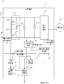
- FIG. 1 is a block diagram showing the configuration of a power converter according to an embodiment
- FIG. FIG. 2 is a block diagram showing the hardware configuration of the power conversion device according to the embodiment
- 3 is a flowchart showing an example of switching element control operation performed by the control device according to the embodiment
- FIG. 4 is a diagram showing an example of the relationship between the detected voltage value and the target duty factor in the embodiment
- 4 is a timing chart showing the operation of the control device according to the embodiment, wherein (A) shows the power consumption control signal, (B) shows the actual current flowing through the conductor, (C) shows the sampling timing, ( D) is a timing chart showing current detection values
- FIG. 1 is a block diagram showing the configuration of a power converter according to an embodiment
- FIG. FIG. 2 is a block diagram showing the hardware configuration of the power conversion device according to the embodiment
- 3 is a flowchart showing an example of switching element control operation performed by the control device according to the embodiment
- FIG. 4 is a diagram showing an example of the relationship between the
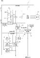
- FIG. 2 is a block diagram showing the configuration of a first modified example of the power conversion device according to the embodiment;
- FIG. 11 is a block diagram showing the configuration of a third modified example of the power conversion device according to the embodiment;
- 4 is a timing chart showing a first modification of the operation of the control device according to the embodiment, where (A) shows the power consumption control signal, (B) shows the actual current flowing through the conductor, and (C) shows the sampling Timing chart showing timing, (D) showing current detection value
- FIG. 4 is a timing chart showing a second modification of the operation of the control device according to the embodiment, where (A) shows the power consumption control signal, (B) shows the actual current flowing through the conductor, and (C) shows the sampling Timing chart showing timing, (D) showing current detection value
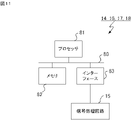
- FIG. 4 is a block diagram showing a modification of the hardware configuration of the power conversion device according to the embodiment
- An example of an electronic device is a DC-three-phase converter installed in a railway vehicle that converts DC power supplied from a power supply into three-phase AC power and supplies it to load equipment.
- An electronic device 1 according to Embodiment 1 will be described by taking a DC-three-phase converter mounted on a railway vehicle as an example.
- the electronic device 1 shown in FIG. 1 is mounted on a railway vehicle of a DC feeding system.
- the electric motor 91 that receives the three-phase AC power supply from the electronic device 1 is a three-phase induction motor that is driven by receiving the three-phase AC power supply to generate the propulsion force of the railway vehicle. Specifically, when the electric motor 91 is driven, it powers the axle of the rail vehicle through couplings, gears, and the like.
- the electronic device 1 includes an input terminal 1a connected to a power supply and an input terminal 1b grounded.
- the electronic device 1 further converts the DC power supplied from the power source into three-phase AC power and supplies the three-phase AC power to the electric motor 91, or the three-phase AC power supplied from the electric motor 91 operating as a generator. to DC power and outputting the DC power, and a power conversion circuit control unit 12 for controlling the power conversion circuit 11 .
- the electronic device 1 further includes a capacitor C1 connected between a pair of primary terminals connected to the input terminals 1a and 1b of the power conversion circuit 11, a power consumption circuit 13 that consumes the power supplied from the capacitor C1, and a control device 14 for controlling the power consumption circuit 13 .
- the electronic device 1 further includes a voltage sensor VT1 which is connected in parallel to the capacitor C1 and measures the value of the voltage applied to the capacitor C1, a current sensor CT1 which measures the value of the current flowing through the power consumption circuit 13, and a voltage sensor. and a signal processing circuit 15 for converting the measured values of VT1 and current sensor CT1 into digital data.
- the input terminal 1a is electrically connected via a contactor, reactor, etc. (not shown) to a power source, specifically, a current collector that acquires power supplied from a substation via a power supply line.
- a current collector is a pantograph that acquires power through an overhead wire, which is an example of a power supply line, or a collector shoe that acquires power through a third rail, which is an example of a power supply line.
- the input terminal 1b is grounded via a grounding ring, grounding brush, wheel, etc., not shown.
- the power conversion circuit 11 is formed by, for example, an inverter whose output AC power has a variable effective voltage and frequency.
- the power conversion circuit 11 has a plurality of switching elements, and the switching operation of each switching element is controlled by the power conversion circuit control section 12 .
- Each switching element is formed of, for example, an IGBT (Insulated Gate Bipolar Transistor).
- the power conversion circuit control unit 12 acquires the operation command S1 from the cab (not shown).
- the operation command S1 indicates a command according to the operator's operation to the master controller provided in the cab. Specifically, the operation command S1 indicates one of a powering command, a braking command, and a coasting command.
- the power conversion circuit control unit 12 generates and outputs a power conversion control signal S2 for controlling each switching element of the power conversion circuit 11 according to the operation command S1.
- the power conversion control signal S2 is, for example, a PWM (Pulse Width Modulation) signal.
- One end of the capacitor C1 is connected to a connection point between the input terminal 1a and one primary terminal of the power conversion circuit 11 .
- the other end of the capacitor C1 is connected to the connection point between the input terminal 1b and the other primary terminal of the power conversion circuit 11 .
- the capacitor C ⁇ b>1 is charged with the DC power supplied from the power supply or the DC power output from the power conversion circuit 11 .
- a voltage sensor VT1 is provided in parallel with the capacitor C1.
- the voltage sensor VT1 is formed of, for example, a VT (Voltage Transformer).
- the voltage sensor VT1 measures the value of the voltage applied to the capacitor C1 and outputs a voltage sensor signal indicating the measured value as analog data.
- the power consumption circuit 13 is connected in parallel with the capacitor C1.
- the power consumption circuit 13 has a switching element SW1 and a resistor R1 connected in series.
- the switching element SW1 is formed of, for example, an IGBT.
- the switching element SW1 switches between a conducting state and a non-conducting state of a conductor electrically connected to the switching element SW1, for example, a conductor 20 electrically connecting the emitter terminal of the switching element SW1 and the resistor R1. Specifically, when switching element SW1 is turned on, conductor 20 is in a conducting state, and when switching element SW1 is turned off, conductor 20 is in a non-conducting state.
- the capacitor C1 When the switching element SW1 is turned on by the switching operation described above, the capacitor C1 is electrically connected to the resistor R1, and the power supplied from the capacitor C1 is consumed by the resistor R1. As a result, the capacitor C1 is discharged and the value of the voltage applied to the capacitor C1 decreases. When the switching element SW1 is turned off, the capacitor C1 and the resistor R1 are electrically disconnected.
- the current sensor CT1 provided in the power consumption circuit 13 has, for example, a CT (Current Transformer) attached to a conductor 20 that is a busbar electrically connecting the switching element SW1 and the resistor R1.
- the current sensor CT1 measures the value of the current flowing through the conductor 20 and outputs a current sensor signal indicating the measured value as analog data.
- the signal processing circuit 15 samples the voltage sensor signal output by the voltage sensor VT1 and the current sensor signal output by the current sensor CT1 every sampling cycle, and outputs digital data indicating the detected value. Specifically, the signal processing circuit 15 detects the measured value indicated by the voltage sensor signal output by the voltage sensor VT1 in each sampling cycle, and detects the voltage detection value V1 which is digital data indicating the value of the voltage applied to the capacitor C1. is generated and output to the power conversion circuit control unit 12 and the control device 14 . The signal processing circuit 15 detects the measured value indicated by the current sensor signal output by the current sensor CT1 for each sampling period, generates the current detection value I1 which is digital data indicating the value of the direct current flowing through the conductor 20, and controls the Output to device 14 .
- the control device 14 turns on the switching element SW1 for an on-time determined by the target duty factor determining unit 21 that determines the target duty factor indicating the target value of the duty factor of the switching element SW1, and the target duty factor and the switching period. and a current value measuring unit 23 for measuring the value of the current flowing through the conductor 20 from the current detection value I1.
- the duty ratio determination unit 21 acquires the operation command S1 from the cab.
- the duty ratio determination unit 21 determines and outputs a target duty ratio according to the value of the voltage applied to the capacitor C1 when the operation command S1 includes a brake command.
- the duty ratio of the switching element SW1 is a value equal to or greater than 0 and equal to or less than 1, and represents the ratio of the time during which the switching element SW1 is turned on with respect to the switching period of the switching element SW1.
- the element control unit 22 acquires the target duty ratio from the duty ratio determination unit 21, and turns on the switching element SW1 for an ON time determined by the target duty ratio and the switching period. Specifically, based on a reference signal output from an oscillator (not shown), the element control unit 22 turns ON for an ON time determined by the target duty factor and the switching period within the switching period determined by the period of the reference signal.
- a power consumption control signal S3, which is a PWM signal, is generated. The ON time is a value obtained by multiplying the switching period by the target duty ratio. Then, the element control section 22 outputs the power consumption control signal S3 to the switching element SW1.
- the element control unit 22 controls the detection duty factor, which is a value of 1 or less higher than the target duty factor in at least one switching period, and the switching period.
- a power consumption control signal S3 that is turned on for a determined on-time is generated.
- the element control section 22 uses the value obtained by multiplying the target duty ratio by a coefficient of 1 or more and the lower value of 1 as the duty ratio for detection.
- the current value measurement unit 23 measures the value of the current flowing through the conductor 20 from the current detection value I1. More specifically, the current value measurement unit 23 multiplies the current detection value I1 by the turns ratio of CT of the current sensor CT1, and uses the multiplication result as the measured value of the current flowing through the conductor 20. FIG. Then, the current value measuring unit 23 sends the measured value of the current flowing through the conductor 20 to a monitoring device, such as a train information management system, for monitoring whether the value of the current flowing through the conductor 20 is overcurrent. Output.
- a monitoring device such as a train information management system
- the control device 14 having the above configuration is realized by a processing circuit 71 as shown in FIG.
- the processing circuit 71 is connected via an interface circuit 72 to the signal processing circuit 15, a cab (not shown in FIG. 2), the switching element SW1 of the power consumption circuit 13, and the like.
- the processing circuit 71 may be, for example, a single circuit, a composite circuit, a processor, an ASIC (Application Specific Integrated Circuit), an FPGA (Field Programmable Gate Array), or a combination thereof. is.
- Each part of the control device 14 may be realized by a separate processing circuit 71 , or each part of the control device 14 may be realized by a common processing circuit 71 .
- the operation of the electronic device 1 having the above configuration will be described below.
- the operation command S1 includes a power running command
- the electric motor 91 is driven by being supplied with three-phase AC power to generate propulsion force for the railway vehicle.
- the power conversion circuit control unit 12 acquires the value of the phase current flowing in the electric motor 91 measured by a current sensor (not shown), and the acceleration of the railcar indicated by the powering command.
- a target torque which is a target value of the torque of the electric motor 91, is determined according to the target value and the value of the phase current.
- the power inverter circuit control unit 12 determines a voltage command value indicating a target value of the output voltage of the power inverter circuit 11 for obtaining the target torque.
- the power conversion circuit control unit 12 generates and outputs a power conversion control signal S2 for controlling the switching operation of each switching element included in the power conversion circuit 11 according to the voltage command value.
- each switching element When the power conversion control signal S2 is supplied to the gate signal of each switching element of the power conversion circuit 11, each switching element performs a switching operation. As a result, the power conversion circuit 11 converts the DC power into three-phase AC power and supplies the three-phase AC power to the electric motor 91 .
- the electric motor 91 operating as a generator supplies the electronic device 1 with three-phase AC power.
- the electronic device 1 converts the three-phase AC power supplied from the electric motor 91 into DC power, and runs in the vicinity of the railcar on which the electronic device 1 is mounted via the current collector and the power supply line. Provides DC power to other rail vehicles.
- a regenerative braking force for decelerating the railway vehicles is generated.
- the power conversion circuit control unit 12 acquires the voltage detection value V1 from the signal processing circuit 15, and the power conversion circuit 11 from the electric motor 91 measured by a current sensor (not shown). Get the value of the phase current flowing through Then, the power inverter circuit control unit 12 determines a voltage command value indicating a target value of the output voltage of the power inverter circuit 11 according to the detected voltage value V1 and the value of the phase current flowing from the electric motor 91 to the power inverter circuit 11. .
- the target value of the output voltage of the power conversion circuit 11 is, for example, a voltage range higher than the overhead line voltage and a value included in the target voltage range indicating the voltage range in which regenerative braking can be used. Then, the power conversion circuit control unit 12 generates and outputs a power conversion control signal S2 for controlling the switching operation of each switching element included in the power conversion circuit 11 according to the voltage command value.
- each switching element When the power conversion control signal S2 is supplied to the gate signal of each switching element of the power conversion circuit 11, each switching element performs a switching operation. As a result, the power conversion circuit 11 converts the three-phase AC power supplied from the electric motor 91 into DC power, and charges the capacitor C1 with the DC power.
- step S11 When the control device 14 acquires the operation command S1, it starts the operation shown in FIG. If the operation command S1 does not include a brake command (step S11; No), the process of step S11 is repeated.
- the operation command S1 includes a brake command (step S11; Yes)
- the duty ratio determination unit 21 determines a target duty ratio indicating a target value of the duty ratio of the switching element SW1 according to the voltage detection value V1. (step S12).
- the duty ratio determining unit 21 determines the target duty ratio based on the relationship between the predetermined voltage detection value V1 and the target duty ratio, as shown in FIG. 4, for example. For example, the duty ratio determining unit 21 sets the target duty ratio to 0 when the detected voltage value V1 is equal to or less than the threshold voltage value Vth1. When the voltage detection value V1 is greater than the threshold voltage value Vth1 and less than the voltage value Vth2, the duty ratio determining unit 21 sets the target duty ratio to the voltage detection value V1 in a state of having a positive correlation. , linearly increase according to the change in the voltage detection value V1.
- the threshold voltage value Vth1 is the voltage value of the capacitor C1 when the capacitor C1 needs to be discharged.
- the duty ratio determining unit 21 sets the target duty ratio to ⁇ 1.
- the duty ratio determining unit 21 sets the target duty ratio to 1 when the detected voltage value V1 becomes equal to or higher than the voltage value Vth2. Then, the duty ratio determination unit 21 sends the target duty ratio determined as described above to the element control unit 22 .
- step S13 in FIG. 3; No If the target duty ratio is not a positive number less than 1 (step S13 in FIG. 3; No), in other words, if the target duty ratio is 0 or 1, the element control unit 22 sets the target value determined in step S12. A power consumption control signal S3 based on the duty ratio is generated and output (step S14). Specifically, the element control section 22 outputs the power consumption control signal S3 that is turned on for an on-time determined by the target duty factor and the switching period. As a result, the switching element SW1 is turned on for an ON time determined by the target duty factor and the switching period in each switching period.
- the element control unit 22 sets the detection duty factor to a value of 1 or less, which is higher than the target duty factor in at least one switching cycle. to generate and output a power consumption control signal S3 (step S15). Specifically, the element control section 22 outputs the power consumption control signal S3 that is turned on for an on-time determined by the duty ratio for detection and the switching period in at least one switching period. As a result, the switching element SW1 is turned on for an on-time determined by the duty ratio for detection and the switching period in at least one switching period. In other words, in at least one switching cycle, the ON time of the switching element SW1 is longer than the ON time determined by the target duty factor and the switching cycle.
- the current value measurement unit 23 measures the value of the current flowing through the conductor 20 according to the current detection value I1 (step S16). After that, the above-described processing is repeated from step S11.
- T1 be the time at which the voltage detection value V1 becomes a voltage value Va higher than the threshold voltage value Vth1.
- T1 the time at which the voltage detection value V1 becomes a voltage value Va higher than the threshold voltage value Vth1.
- T2 a measurement period for measuring the value of the current flowing through conductor 20 is started, and the measurement period ends at time T2.
- the measurement period shall include multiple switching periods.
- ⁇ 1 be the duty ratio when the voltage detection value V1 is Va as shown in FIG.
- the duty ratio determining unit 21 sets the target duty ratio to ⁇ 1.
- the element control unit 22 in the first switching cycle of the measurement period, is turned on for a period of time corresponding to the duty ratio ⁇ 2 for detection that is higher than the target duty ratio ⁇ 1. generates a power consumption control signal S3 that is turned on for a period of time corresponding to the target duty factor ⁇ 1.
- the ON time indicated by the power consumption control signal S3 in the first switching cycle is ⁇ 2 ⁇ 1 obtained by multiplying the duty ratio for detection ⁇ 2 by the switching cycle ⁇ 1.
- the ON time indicated by the power consumption control signal S3 becomes the value ⁇ 1 ⁇ 1 obtained by multiplying the target duty factor ⁇ 1 by the switching period ⁇ 1.
- the switching element SW1 When the power consumption control signal S3 is supplied to the gate terminal of the switching element SW1, the switching element SW1 performs switching operation. Specifically, when the power consumption control signal S3 indicates ON, the switching element SW1 is turned ON. When switching element SW1 is turned on, resistor R1 is electrically connected to capacitor C1 and current flows through conductor 20 and resistor R1. When the power consumption control signal S3 indicates off, the switching element SW1 is turned off. When switching element SW1 is turned off, resistor R1 and capacitor C1 are electrically disconnected and no current flows through conductor 20 and resistor R1.
- FIG. 5B shows an example of the actual current flowing through the conductor 20.
- Ia be the value of the current flowing through the conductor 20 when the switching element SW1 is on.
- the sampling period ⁇ 2 which is the period in which the signal processing circuit 15 detects the measured value indicated by the current sensor signal, is determined based on a clock independent of the switching period. As shown in FIG. 5(C), in the first switching cycle included in the measurement period, the switching element SW1, which is represented by the value ⁇ 2 ⁇ 1 obtained by multiplying the duty factor ⁇ 2 for detection by the switching cycle ⁇ 1, is turned on. A sampling timing, which is a detection timing for each sampling period ⁇ 2, is included in the period in which .
- the signal processing circuit 15 outputs the current value Ia as the current detection value I1, which is the detected value of the current flowing through the conductor 20.
- the sixth sampling timing shown in FIG. 5C is not included in the ON time shown in FIG. A value of the current flowing is detected. Specifically, at the sixth sampling timing shown in FIG. 5(C), the signal processing circuit 15 sets the detected current value I1, which is the detected value of the current flowing through the conductor 20, as shown in FIG. A current value Ia' smaller than the current value Ia is output.
- the current value measurement unit 23 measures the value of the current flowing through the conductor 20 from the maximum value of the current detection value I1 during the measurement period. As shown in FIG. 5(D), the maximum value of the current detection value I1 is the current value Ia. Therefore, the current value measuring unit 23 outputs the result of multiplying the current value Ia by the turns ratio of the CT of the current sensor CT1 as the value of the current flowing through the conductor 20 . After time T2, the measurement period is repeated while the voltage of the capacitor C1, that is, the voltage detection value V1 is higher than the threshold voltage value Vth1, and the above-described processing is repeated.
- the control device when the target duty factor is a positive number less than 1, the value is 1 or less, which is higher than the target duty factor in at least one switching cycle.
- the switching element SW1 is turned on for an on-time determined by the duty ratio for detection and the switching period.
- the period during which the switching element SW1 is turned on becomes longer than the on-time determined by the target duty factor and the switching period. Accordingly, when the current sensor signal output by the current sensor CT1 is detected at the timing when the switching element SW1 is turned on, the value of the current flowing through the conductor 20 can be measured with high accuracy.
- control device 14 may control switching element SW1 according to the measured current value.
- the electronic device 1 shown in FIG. 6 includes a control device 16 that estimates the temperature of the resistor R1.
- the control device 16 further includes a temperature estimation section 24 that estimates the temperature of the resistor R ⁇ b>1 from the current value measured by the current value measurement section 23 .
- the hardware configuration of the control device 16 is the same as that of the control device 14 .
- the temperature estimation unit 24 acquires the voltage detection value V1 from the signal processing circuit 15 and acquires the measured current value from the current value measurement unit 23 .
- the temperature estimator 24 estimates the temperature of the resistor R1 according to the acquired value described above.
- the temperature estimator 24 sends the estimated value of the temperature of the resistor R1 to the element controller 22 .
- the temperature estimator 24 estimates the temperature of the resistor R1 based on the following equation (1).
- T1 indicates the temperature of the resistor R1
- T0 indicates the initial temperature, which is the temperature of the resistor R1 when no current flows through the resistor R1
- ⁇ T indicates the temperature of the resistor R1 due to current flow. It is a temperature rise value and is represented by the following formula (2).
- k indicates a determined temperature coefficient
- V1 indicates a voltage detection value
- Id indicates a current value measured by the current value measuring section 23.
- the temperature estimator 24 holds in advance information about the initial temperature T0 and the temperature coefficient k indicating the amount of temperature rise of the resistor R1 with respect to the amount of power consumption determined by a predetermined temperature rise curve.
- T1 T0+ ⁇ T (1)
- ⁇ T k ⁇ V1 ⁇ Id (2)
- the element control unit 22 When the estimated value of the temperature of the resistor R1 acquired from the temperature estimation unit 24 becomes equal to or higher than the threshold temperature, the element control unit 22 operates the switching element SW1 at a duty ratio lower than the target duty ratio determined by the duty ratio determination unit 21. to control. For example, when the estimated value of the temperature of the resistor R1 obtained from the temperature estimating unit 24 becomes equal to or higher than the threshold temperature, the element control unit 22 sets the target duty factor to 0, generates and outputs the power consumption control signal S3.
- the threshold temperature should be determined according to the temperature range that the element forming the resistor R1 can withstand.
- the threshold temperature may be a value obtained by multiplying the upper limit of the temperature that the element forming the resistor R1 can withstand by 0.8.
- the electronic device 1 shown in FIG. 7 includes a control device 17 that estimates the power consumption of the resistor R1.
- the control device 17 further includes a power consumption estimating section 25 that estimates the power consumption in the resistor R1 from the current value measured by the current value measuring section 23 .
- the hardware configuration of the control device 17 is the same as that of the control device 14 .
- the power consumption estimation unit 25 acquires the voltage detection value V1 from the signal processing circuit 15, acquires the measured current value from the current value measurement unit 23, and receives the switching element SW1 from the element control unit 22. Get the time you are Based on the obtained value, the power consumption estimator 25 estimates the power consumption of the resistor R1 during the measurement period. The power consumption estimator 25 then sends the estimated power consumption to the element controller 22 .
- the power consumption estimator 25 calculates the power consumption of the resistor R1 during the measurement period based on the following equation (3).
- W1 indicates the power consumption of the resistor R1
- V1 indicates the voltage detection value
- Id indicates the current value measured by the current value measuring unit 23
- the element control unit 22 When the power consumption of the resistor R1 acquired from the power consumption estimation unit 25 becomes equal to or greater than the threshold power amount, the element control unit 22 performs switching at a duty ratio lower than the target duty ratio determined by the duty ratio determination unit 21. It controls the element SW1. For example, when the power consumption of the resistor R1 obtained from the power consumption estimating unit 25 becomes equal to or greater than the threshold power, the element control unit 22 sets the target duty factor to 0, and sets the on-state current determined by the target duty factor and the switching cycle. It generates and outputs a power consumption control signal S3 that is turned on only for a period of time.
- the temperature of the resistor R1 rises in proportion to the multiplication result of the voltage detection value V1 and the current value Id measured by the current value measuring section 23.
- the temperature of the resistor R1 rises in proportion to the amount of power consumption, so the threshold power amount should be determined according to the temperature range that the element forming the resistor R1 can withstand.
- the threshold power amount may be a value obtained by dividing the amount of temperature rise that the element forming the resistor R1 can withstand by the temperature coefficient k and multiplying the value by 0.8.
- the element control unit 22 controls the switching element SW1, thereby increasing the power consumption of the resistor R1 and suppressing an excessive rise in the temperature of the resistor R1.
- the power consumption estimator 25 estimates the power consumption of the resistor R1 during the measurement period.
- the power consumption estimator 25 may estimate the power consumption of the resistor R1 in an estimation period, which is a period including the measurement period and for estimating the power consumption.
- the electronic device 1 shown in FIG. 8 includes a control device 18 that estimates the temperature of the resistor R1 and estimates the power consumption at the resistor R1.
- the control device 18 includes both the temperature estimating section 24 and the power consumption estimating section 25 described above.
- the hardware configuration of the control device 18 is the same as that of the control device 14 .
- the element control unit 22 When the estimated value of the temperature of the resistor R1 is equal to or higher than the threshold temperature, or when the estimated value of the power consumption is equal to or higher than the threshold power, the element control unit 22 It generates and outputs a power consumption control signal S3 that is turned on for an on-time determined by the current rate and the switching period.
- the duty ratio determining unit 21 may be provided as a device independent of the control devices 14, 16-18.
- the control devices 14, 16-18 may perform the above-described control according to the target duty ratio acquired from the duty ratio determination unit 21.
- the adjustment of the duty ratio of the switching element SW1 by the element control section 22 is not limited to the above example.
- the element control section 22 may control the switching element SW1 in accordance with the detection duty factor in each successive switching cycle.
- the view of FIG. 9 is the same as that of FIG.
- the element control section 22 controls a detection pass rate higher than the target duty factor ⁇ 1 in a plurality of consecutive switching periods included in the measurement period, specifically, in three consecutive switching periods.
- a power consumption control signal S3 is generated which is turned on for a period of time determined by the current rate ⁇ 3 and the switching period, and is turned on in the subsequent switching period for a period of time determined by the target duty factor ⁇ 1 and the switching period. For example, if the switching cycle is ⁇ 1, the ON time indicated by the power consumption control signal S3 in three consecutive switching cycles is the value ⁇ 3 ⁇ 1 obtained by multiplying the duty ratio for detection ⁇ 3 by the switching cycle ⁇ 1. . In the subsequent switching period, the ON time indicated by the power consumption control signal S3 becomes the value ⁇ 1 ⁇ 1 obtained by multiplying the target duty factor ⁇ 1 by the switching period ⁇ 1.
- FIG. 9A shows an example of the actual current flowing through the conductor 20.
- Ia be the value of the current flowing through the conductor 20 when the switching element SW1 is on.
- the sampling period ⁇ 2 is determined based on a clock that is independent of the switching period.
- the sampling timing which is the detection timing for each sampling cycle, is included in the period in which the switching element SW1 is turned on.
- the signal processing circuit 15 outputs the current value Ia as the current detection value I1, which is the detected value of the current flowing through the conductor 20.
- the current value measurement unit 23 measures the value of the current flowing through the conductor 20 according to the maximum value of the current detection value I1 during the measurement period. As shown in FIG. 9D, the maximum detected current value I1 during the measurement period is the current value Ia. Therefore, the current value measuring unit 23 outputs the result of multiplying the current value Ia by the winding ratio of the CT forming the current sensor CT1 as the value of the current flowing through the conductor 20 .
- the element control section 22 may control the switching element SW1 according to the detection duty factor in each of a plurality of switching cycles spaced apart from each other.
- the view of FIG. 10 is the same as that of FIG.
- the element control section 22 sets the target signal in a plurality of switching cycles included in the measurement period, which are spaced apart from each other, specifically in the first switching cycle and the third switching cycle.
- the power consumption control signal S3 is turned on for a period of time determined by the detection duty factor ⁇ 4 higher than the current rate ⁇ 1 and the switching period, and is turned on for a period of time determined by the target duty factor ⁇ 1 and the switching period in the other switching periods.
- the ON time indicated by the power consumption control signal S3 in the first switching cycle and the third switching cycle is a value ⁇ 4 obtained by multiplying the detection duty ratio ⁇ 4 by the switching cycle ⁇ 1 ⁇ It becomes ⁇ 1.
- the ON time indicated by the power consumption control signal S3 is a value ⁇ 1 ⁇ 1 obtained by multiplying the target duty factor ⁇ 1 by the switching cycle ⁇ 1.
- FIG. 10A shows an example of the actual current flowing through the conductor 20.
- Ia be the value of the current flowing through the conductor 20 when the switching element SW1 is on.
- the sampling period ⁇ 2 is determined based on a clock that is independent of the switching period. Among a plurality of switching cycles in which the switching element SW1 is turned on for a time of ⁇ 4 ⁇ 1 obtained by multiplying the switching cycle ⁇ 1 by the duty factor ⁇ 4 for detection, the switching element SW1 is turned ON in the third switching cycle.
- a sampling timing which is a detection timing for each sampling period, is included in the period of .
- the signal processing circuit 15 outputs the current value Ia as the current detection value I1, which is the detected value of the current flowing through the conductor 20.
- the current value measurement unit 23 measures the value of the current flowing through the conductor 20 according to the maximum value of the current detection value I1 during the measurement period. As shown in FIG. 10(D), the maximum value of the current detection value I1 among the measured values is the current value Ia. Therefore, the current value measuring unit 23 outputs the result of multiplying the current value Ia by the winding ratio of the CT forming the current sensor CT1 as the value of the current flowing through the conductor 20 .
- the element control unit 22 may adjust the duty ratio as described above only when the target duty ratio is equal to or lower than the threshold duty ratio. Specifically, when the target duty factor is higher than the threshold duty factor, the element control unit 22 generates the power consumption control signal S3 based on the target duty factor, and the target duty factor is equal to or lower than the threshold duty factor. , the power consumption control signal S3 may be generated based on the duty ratio for detection.
- the threshold duty factor may be determined according to the switching period and the sampling period.
- the duty ratio of the switching element SW1 when the ON time of the switching element SW1 is 1/2 of the sampling period may be used as the threshold duty factor.
- the element control section 22 may use a fixed value higher than the threshold duty factor as the duty factor for detection.
- the element control unit 22 uses the duty ratio of the switching element SW1 when the ON time of the switching element SW1 matches the sampling period as the threshold duty ratio. good too.
- the element control section 22 may use the same value as the threshold duty factor as the duty factor for detection.
- the duty ratio for detection in this case matches the duty ratio of the switching element SW1 when the ON time of the switching element SW1 matches the sampling period.
- control devices 14, 16, 17, 18 may be realized by software.
- the control devices 14 , 16 , 17 , 18 shown in FIG. 11 are provided with a processor 81 , a memory 82 and an interface 83 .
- Processor 81 , memory 82 and interface 83 are connected to each other by bus 80 .
- control devices 14, 16, 17, 18 are realized by software, firmware, or a combination of software and firmware.
- Software and firmware are written as programs and stored in memory 82 .
- the processor 81 reads out and executes the programs stored in the memory 82 to implement the functions of the above-described units. That is, the memory 82 stores programs for executing processes of the control devices 14 , 16 , 17 and 18 .
- the memory 82 is nonvolatile or volatile such as RAM (Random Access Memory), ROM (Read-Only Memory), flash memory, EPROM (Erasable Programmable Read Only Memory), EEPROM (Electrically Erasable and Programmable Read-Only Memory). semiconductor memories, magnetic discs, flexible discs, optical discs, compact discs, mini discs, DVDs (Digital Versatile Discs), etc.
- control devices 14, 16, 17, and 18 may be realized by dedicated hardware, and another part may be realized by software or firmware.
- the element control section 22 is realized by the processing circuit 71 shown in FIG. It may be realized by reading and executing a program.
- the current values to be measured by the control devices 14, 16, 17, and 18 are not limited to the above examples, and may be any conductor that switches between a conducting state and a non-conducting state by the switching operation of the switching element.
- the power conversion circuit 11 is not limited to the above example, and may be, for example, a DC (Direct Current)-DC converter or a 3-level inverter.
- the capacitor C1 may be a capacitor unit formed of a plurality of capacitors.
- the duty factor determining unit 21 may determine the target duty factor according to the voltage between the terminals of the capacitor unit.
- the configuration of the power consumption circuit 13 is not limited to the above example.
- the power consumption circuit 13 may have a plurality of resistors R1 and a plurality of switching elements SW1 each connected to a corresponding resistor.
- the element control section 22 supplies the power consumption control signal S3 to each switching element SW1 included in the power consumption circuit 13 .
- the element control unit 22 selects the switching element connected to the resistor R1 whose estimated temperature value is higher than the threshold temperature.
- SW1 may be turned off and the switching element SW1 connected to another resistor R1 may be turned on.
- the electronic device 1 is not limited to a power conversion device, but any electronic device including a capacitor C1 and a power consumption circuit 13.
- a railway vehicle on which the electronic device 1 is mounted may use only the generated braking force as the electric braking force without using the regenerative braking force.
- the electronic device 1 is not limited to being mounted on a railway vehicle of a DC feeding system, and may be mounted on a railway vehicle of an AC feeding system. In this case, the electronic device 1 may convert the DC power supplied from the current collector via the transformer and the converter into three-phase AC power and supply the three-phase AC power to the electric motor 91 .
- the electronic device 1 is not limited to railway vehicles, and may be mounted on moving bodies such as automobiles, ships, and airplanes. Alternatively, the electronic device 1 may be installed indoors or outdoors.
Landscapes
- Engineering & Computer Science (AREA)
- Power Engineering (AREA)
- Transportation (AREA)
- Mechanical Engineering (AREA)
- Electric Propulsion And Braking For Vehicles (AREA)
- Control Of Ac Motors In General (AREA)
- Dc-Dc Converters (AREA)
Abstract
Description
通流率決定部21は、運転台から運転指令S1を取得する。通流率決定部21は、運転指令S1がブレーキ指令を含む場合に、コンデンサC1に印加される電圧の値に応じて目標通流率を決定し、出力する。スイッチング素子SW1の通流率は、0以上かつ1以下の値であって、スイッチング素子SW1のスイッチング周期に対するスイッチング素子SW1がオンとなる時間の比率を表す。
運転指令S1が力行指令を含む場合、図1に示す電子機器1は、入力端子1a,1bを介して供給される直流電力を三相交流電力に変換し、三相交流電力を電動機91に供給する。電動機91は、三相交流電力の供給を受けて駆動され、鉄道車両の推進力を生じさせる。
T1=T0+ΔT ・・・(1)
ΔT=k・V1・Id ・・・(2)
W1=V1・Id・t1 ・・・(3)
Claims (14)
- 導体に接続され、スイッチング動作によって前記導体の導通状態と非導通状態とを切り替えるスイッチング素子を制御する制御装置であって、
スイッチング周期に対する前記スイッチング素子がオンとなる時間の比率を表す通流率の目標値を示す目標通流率が1未満の正数である場合に、少なくとも1回の前記スイッチング周期において前記目標通流率より高い1以下の値である検出用通流率と前記スイッチング周期とにより定まる時間だけ前記スイッチング素子をオンにする素子制御部と、
前記導体に流れる直流電流の値を測定する電流センサが出力するアナログデータである電流センサ信号を前記スイッチング周期とは独立したサンプリング周期ごとに検出することで生成されたデジタルデータである電流検出値から前記導体に流れる直流電流の値を測定する電流値測定部と、
を備える制御装置。 - 前記電流値測定部は、前記直流電流の値を測定するための期間であって複数の前記スイッチング周期を含む測定期間における前記電流検出値の最大値から、前記導体に流れる直流電流の値を測定する、
請求項1に記載の制御装置。 - 前記素子制御部は、前記測定期間に含まれる最初の前記スイッチング周期において、前記検出用通流率と前記スイッチング周期とにより定まる時間だけ前記スイッチング素子をオンにし、前記測定期間に含まれる他の前記スイッチング周期において、前記目標通流率と前記スイッチング周期とにより定まる時間だけ前記スイッチング素子をオンにする、
請求項2に記載の制御装置。 - 前記素子制御部は、前記測定期間に含まれる連続する複数の前記スイッチング周期のそれぞれにおいて、前記検出用通流率と前記スイッチング周期とにより定まる時間だけ前記スイッチング素子をオンにし、前記測定期間に含まれる他の前記スイッチング周期において、前記目標通流率と前記スイッチング周期とにより定まる時間だけ前記スイッチング素子をオンにする、
請求項2に記載の制御装置。 - 前記素子制御部は、前記測定期間に含まれる互いに間隔が空いている複数の前記スイッチング周期のそれぞれにおいて、前記検出用通流率と前記スイッチング周期とにより定まる時間だけ前記スイッチング素子をオンにし、前記測定期間に含まれる他の前記スイッチング周期において、前記目標通流率と前記スイッチング周期とにより定まる時間だけ前記スイッチング素子をオンにする、
請求項2に記載の制御装置。 - 前記素子制御部は、前記少なくとも1回の前記スイッチング周期において、前記スイッチング素子がオンとなる時間が前記サンプリング周期に一致する場合の前記スイッチング素子の通流率に一致する前記検出用通流率に応じて前記スイッチング素子を制御する、
請求項1から5のいずれか1項に記載の制御装置。 - 前記スイッチング素子は、前記導体を介して接続される抵抗をコンデンサに電気的に接続し、または前記抵抗を前記コンデンサから電気的に切り離す、
請求項1から6のいずれか1項に記載の制御装置。 - 前記素子制御部は、前記コンデンサに印加される電圧の値が閾値電圧値を超えると開始される前記測定期間に含まれる少なくとも1回の前記スイッチング周期において前記検出用通流率と前記スイッチング周期とにより定まる時間だけ前記スイッチング素子をオンにする、
請求項7に記載の制御装置。 - 前記素子制御部は、前記コンデンサの電圧が閾値電圧を超えている間に定められた時間ごとに繰り返される前記測定期間に含まれる少なくとも1回の前記スイッチング周期において前記検出用通流率に応じて前記スイッチング素子を制御する、
請求項7に記載の制御装置。 - 前記コンデンサに印加される電圧の値、および前記電流値測定部で測定された前記導体に流れる直流電流の値から前記抵抗の温度を推定する温度推定部をさらに備える、
請求項7から9のいずれか1項に記載の制御装置。 - 前記電流値測定部で測定された前記導体に流れる直流電流の値、前記コンデンサに印加される電圧の値、および、前記測定期間における前記スイッチング素子がオンになっている時間の合計値から、前記測定期間における前記抵抗での消費電力量を推定する消費電力量推定部をさらに備える、
請求項7から10のいずれか1項に記載の制御装置。 - 直流電力で充電されるコンデンサと、
抵抗と、前記抵抗に直列に接続され、前記抵抗を前記コンデンサに電気的に接続し、または前記抵抗を前記コンデンサから電気的に切り離すスイッチング素子と、を有し、前記コンデンサに並列に接続される電力消費回路と、
前記抵抗と前記スイッチング素子とを電気的に接続する導体に流れる直流電流の値を測定し、測定した前記直流電流の値を示すアナログデータである電流センサ信号を出力する電流センサと、
請求項1から11のいずれか1項に記載の制御装置と、を備え、
前記制御装置は、前記電力消費回路が有する前記スイッチング素子を制御する、
電子機器。 - 鉄道車両に搭載され、
前記コンデンサを介して供給される直流電力を前記鉄道車両の推進力を生じさせる電動機に供給するための電力に変換し、変換した電力を前記電動機に供給し、または、発電機として動作する前記電動機から供給される電力を直流電力に変換し、変換した直流電力で前記コンデンサを充電する電力変換回路をさらに備え、
前記鉄道車両の減速時に、前記素子制御部は、前記コンデンサに印加される電圧の値により定まる前記目標通流率が1未満の正数である場合に、少なくとも1回の前記スイッチング周期において前記検出用通流率と前記スイッチング周期とにより定まる時間だけ前記スイッチング素子をオンにする、
請求項12に記載の電子機器。 - 導体に接続され、スイッチング動作によって前記導体の導通状態と非導通状態とを切り替えるスイッチング素子を、スイッチング周期に対する前記スイッチング素子がオンとなる時間の比率を表す通流率の目標値を示す目標通流率が1未満の正数である場合に、少なくとも1回の前記スイッチング周期において前記目標通流率より高い1以下の値である検出用通流率と前記スイッチング周期とにより定まる時間だけ前記スイッチング素子をオンにし、
前記導体に流れる直流電流の値を示すアナログデータである電流センサ信号を前記スイッチング周期とは独立したサンプリング周期ごとに検出することで生成されたデジタルデータである電流検出値から前記導体に流れる直流電流の値を測定する、
制御方法。
Priority Applications (4)
| Application Number | Priority Date | Filing Date | Title |
|---|---|---|---|
| JP2023534536A JP7433538B2 (ja) | 2021-07-15 | 2021-07-15 | 制御装置、電子機器および制御方法 |
| US18/561,479 US12483177B2 (en) | 2021-07-15 | 2021-07-15 | Control device, electronic apparatus, and control method |
| PCT/JP2021/026590 WO2023286233A1 (ja) | 2021-07-15 | 2021-07-15 | 制御装置、電子機器および制御方法 |
| DE112021007970.0T DE112021007970T5 (de) | 2021-07-15 | 2021-07-15 | Steuerungseinrichtung, elektronische vorrichtung und steuerungsverfahren |
Applications Claiming Priority (1)
| Application Number | Priority Date | Filing Date | Title |
|---|---|---|---|
| PCT/JP2021/026590 WO2023286233A1 (ja) | 2021-07-15 | 2021-07-15 | 制御装置、電子機器および制御方法 |
Publications (1)
| Publication Number | Publication Date |
|---|---|
| WO2023286233A1 true WO2023286233A1 (ja) | 2023-01-19 |
Family
ID=84919719
Family Applications (1)
| Application Number | Title | Priority Date | Filing Date |
|---|---|---|---|
| PCT/JP2021/026590 Ceased WO2023286233A1 (ja) | 2021-07-15 | 2021-07-15 | 制御装置、電子機器および制御方法 |
Country Status (4)
| Country | Link |
|---|---|
| US (1) | US12483177B2 (ja) |
| JP (1) | JP7433538B2 (ja) |
| DE (1) | DE112021007970T5 (ja) |
| WO (1) | WO2023286233A1 (ja) |
Families Citing this family (1)
| Publication number | Priority date | Publication date | Assignee | Title |
|---|---|---|---|---|
| CN120009744B (zh) * | 2025-04-17 | 2025-07-25 | 浙江上青元电力科技有限公司 | 一种蓄电池智能监测系统 |
Citations (4)
| Publication number | Priority date | Publication date | Assignee | Title |
|---|---|---|---|---|
| JP2003018877A (ja) * | 2001-06-29 | 2003-01-17 | Hitachi Ltd | 冷蔵庫 |
| JP2007255884A (ja) * | 2007-02-06 | 2007-10-04 | Hitachi Appliances Inc | 空気調和機 |
| JP2011130619A (ja) * | 2009-12-21 | 2011-06-30 | Daifuku Co Ltd | 無接触給電設備の電源装置 |
| WO2019049188A1 (ja) * | 2017-09-05 | 2019-03-14 | 株式会社日立製作所 | 交流電動機の監視装置および監視方法、ならびに電動機駆動システムの監視装置および監視方法 |
Family Cites Families (3)
| Publication number | Priority date | Publication date | Assignee | Title |
|---|---|---|---|---|
| JP2007282379A (ja) | 2006-04-06 | 2007-10-25 | Toshiba Corp | 電気車駆動装置 |
| JP6225942B2 (ja) * | 2015-04-21 | 2017-11-08 | トヨタ自動車株式会社 | 電力変換システム |
| CN113273071B (zh) * | 2019-02-22 | 2024-03-08 | 阿尔卑斯阿尔派株式会社 | 直流电压变换电路以及开关电源装置 |
-
2021
- 2021-07-15 JP JP2023534536A patent/JP7433538B2/ja active Active
- 2021-07-15 WO PCT/JP2021/026590 patent/WO2023286233A1/ja not_active Ceased
- 2021-07-15 US US18/561,479 patent/US12483177B2/en active Active
- 2021-07-15 DE DE112021007970.0T patent/DE112021007970T5/de active Pending
Patent Citations (4)
| Publication number | Priority date | Publication date | Assignee | Title |
|---|---|---|---|---|
| JP2003018877A (ja) * | 2001-06-29 | 2003-01-17 | Hitachi Ltd | 冷蔵庫 |
| JP2007255884A (ja) * | 2007-02-06 | 2007-10-04 | Hitachi Appliances Inc | 空気調和機 |
| JP2011130619A (ja) * | 2009-12-21 | 2011-06-30 | Daifuku Co Ltd | 無接触給電設備の電源装置 |
| WO2019049188A1 (ja) * | 2017-09-05 | 2019-03-14 | 株式会社日立製作所 | 交流電動機の監視装置および監視方法、ならびに電動機駆動システムの監視装置および監視方法 |
Also Published As
| Publication number | Publication date |
|---|---|
| JP7433538B2 (ja) | 2024-02-19 |
| US12483177B2 (en) | 2025-11-25 |
| JPWO2023286233A1 (ja) | 2023-01-19 |
| DE112021007970T5 (de) | 2024-07-04 |
| US20240258946A1 (en) | 2024-08-01 |
Similar Documents
| Publication | Publication Date | Title |
|---|---|---|
| CN102998017B (zh) | 功率半导体装置的温度测量设备 | |
| US20130258734A1 (en) | Apparatus for controlling voltage converting apparatus | |
| US10250124B2 (en) | Power converter for controlling switching elements during regenerative control of an inverter | |
| JP5488097B2 (ja) | 電流推定装置およびdcdcコンバータ制御システム | |
| JP6972343B2 (ja) | 鉄道車両用制御装置および離線判定方法 | |
| JP2012090406A (ja) | スイッチング電源装置 | |
| US20150108930A1 (en) | Converter for an electric motor | |
| JP6184335B2 (ja) | 電力変換装置及び故障予兆検出方法 | |
| JP2019527027A (ja) | 電流コンバータの駆動方法およびその方法で駆動される電流コンバータ | |
| CN110506387A (zh) | 用于连接至公共总线的逆变器的电流减小系统 | |
| KR102441606B1 (ko) | 모터 제어 시스템 및 그 방법 | |
| JP7433538B2 (ja) | 制御装置、電子機器および制御方法 | |
| US9502977B2 (en) | Control apparatus for voltage converting apparatus | |
| KR102177720B1 (ko) | 인버터 구동용 전류센서의 옵셋 보상 장치 및 이의 방법 | |
| CN110710091B (zh) | Dc/dc转换器的控制装置 | |
| JP2016021845A (ja) | 充電装置及び充電制御装置 | |
| JP2009296846A (ja) | 車両用インバータ装置 | |
| JP2012013433A (ja) | 電圧検出回路及び電力供給装置 | |
| CN112004713B (zh) | 馈电装置以及馈电系统 | |
| JP6937913B2 (ja) | 鉄道車両用制御装置 | |
| JP2012157145A (ja) | 双方向コンバータ、その制御回路およびその制御方法 | |
| JP7294071B2 (ja) | 電源システム | |
| JPH1198857A (ja) | 多重パルス幅変調方式を用いた電力変換装置 | |
| CN114257106A (zh) | 用于连接至公共总线的转换器的降谐波失真系统 | |
| JP6210031B2 (ja) | 制御装置 |
Legal Events
| Date | Code | Title | Description |
|---|---|---|---|
| 121 | Ep: the epo has been informed by wipo that ep was designated in this application |
Ref document number: 21950172 Country of ref document: EP Kind code of ref document: A1 |
|
| ENP | Entry into the national phase |
Ref document number: 2023534536 Country of ref document: JP Kind code of ref document: A |
|
| WWE | Wipo information: entry into national phase |
Ref document number: 18561479 Country of ref document: US |
|
| WWE | Wipo information: entry into national phase |
Ref document number: 202427000488 Country of ref document: IN |
|
| 122 | Ep: pct application non-entry in european phase |
Ref document number: 21950172 Country of ref document: EP Kind code of ref document: A1 |
|
| WWG | Wipo information: grant in national office |
Ref document number: 18561479 Country of ref document: US |