WO2023282013A1 - 半導体装置 - Google Patents
半導体装置 Download PDFInfo
- Publication number
- WO2023282013A1 WO2023282013A1 PCT/JP2022/024140 JP2022024140W WO2023282013A1 WO 2023282013 A1 WO2023282013 A1 WO 2023282013A1 JP 2022024140 W JP2022024140 W JP 2022024140W WO 2023282013 A1 WO2023282013 A1 WO 2023282013A1
- Authority
- WO
- WIPO (PCT)
- Prior art keywords
- semiconductor device
- electrode
- covering portion
- metal
- wire
- Prior art date
- Legal status (The legal status is an assumption and is not a legal conclusion. Google has not performed a legal analysis and makes no representation as to the accuracy of the status listed.)
- Ceased
Links
Images


Classifications
-
- H—ELECTRICITY
- H10—SEMICONDUCTOR DEVICES; ELECTRIC SOLID-STATE DEVICES NOT OTHERWISE PROVIDED FOR
- H10W—GENERIC PACKAGES, INTERCONNECTIONS, CONNECTORS OR OTHER CONSTRUCTIONAL DETAILS OF DEVICES COVERED BY CLASS H10
- H10W70/00—Package substrates; Interposers; Redistribution layers [RDL]
- H10W70/40—Leadframes
- H10W70/461—Leadframes specially adapted for cooling
-
- H—ELECTRICITY
- H10—SEMICONDUCTOR DEVICES; ELECTRIC SOLID-STATE DEVICES NOT OTHERWISE PROVIDED FOR
- H10W—GENERIC PACKAGES, INTERCONNECTIONS, CONNECTORS OR OTHER CONSTRUCTIONAL DETAILS OF DEVICES COVERED BY CLASS H10
- H10W40/00—Arrangements for thermal protection or thermal control
- H10W40/70—Fillings or auxiliary members in containers or in encapsulations for thermal protection or control
-
- H—ELECTRICITY
- H10—SEMICONDUCTOR DEVICES; ELECTRIC SOLID-STATE DEVICES NOT OTHERWISE PROVIDED FOR
- H10W—GENERIC PACKAGES, INTERCONNECTIONS, CONNECTORS OR OTHER CONSTRUCTIONAL DETAILS OF DEVICES COVERED BY CLASS H10
- H10W70/00—Package substrates; Interposers; Redistribution layers [RDL]
- H10W70/40—Leadframes
- H10W70/464—Additional interconnections in combination with leadframes
- H10W70/465—Bumps or wires
-
- H—ELECTRICITY
- H10—SEMICONDUCTOR DEVICES; ELECTRIC SOLID-STATE DEVICES NOT OTHERWISE PROVIDED FOR
- H10W—GENERIC PACKAGES, INTERCONNECTIONS, CONNECTORS OR OTHER CONSTRUCTIONAL DETAILS OF DEVICES COVERED BY CLASS H10
- H10W70/00—Package substrates; Interposers; Redistribution layers [RDL]
- H10W70/40—Leadframes
- H10W70/481—Leadframes for devices being provided for in groups H10D8/00 - H10D48/00
-
- H—ELECTRICITY
- H10—SEMICONDUCTOR DEVICES; ELECTRIC SOLID-STATE DEVICES NOT OTHERWISE PROVIDED FOR
- H10W—GENERIC PACKAGES, INTERCONNECTIONS, CONNECTORS OR OTHER CONSTRUCTIONAL DETAILS OF DEVICES COVERED BY CLASS H10
- H10W74/00—Encapsulations, e.g. protective coatings
- H10W74/10—Encapsulations, e.g. protective coatings characterised by their shape or disposition
- H10W74/111—Encapsulations, e.g. protective coatings characterised by their shape or disposition the semiconductor body being completely enclosed
- H10W74/121—Encapsulations, e.g. protective coatings characterised by their shape or disposition the semiconductor body being completely enclosed by multiple encapsulations, e.g. by a thin protective coating and a thick encapsulation
-
- H—ELECTRICITY
- H10—SEMICONDUCTOR DEVICES; ELECTRIC SOLID-STATE DEVICES NOT OTHERWISE PROVIDED FOR
- H10W—GENERIC PACKAGES, INTERCONNECTIONS, CONNECTORS OR OTHER CONSTRUCTIONAL DETAILS OF DEVICES COVERED BY CLASS H10
- H10W90/00—Package configurations
-
- H—ELECTRICITY
- H10—SEMICONDUCTOR DEVICES; ELECTRIC SOLID-STATE DEVICES NOT OTHERWISE PROVIDED FOR
- H10W—GENERIC PACKAGES, INTERCONNECTIONS, CONNECTORS OR OTHER CONSTRUCTIONAL DETAILS OF DEVICES COVERED BY CLASS H10
- H10W90/00—Package configurations
- H10W90/811—Multiple chips on leadframes
-
- H—ELECTRICITY
- H10—SEMICONDUCTOR DEVICES; ELECTRIC SOLID-STATE DEVICES NOT OTHERWISE PROVIDED FOR
- H10W—GENERIC PACKAGES, INTERCONNECTIONS, CONNECTORS OR OTHER CONSTRUCTIONAL DETAILS OF DEVICES COVERED BY CLASS H10
- H10W70/00—Package substrates; Interposers; Redistribution layers [RDL]
- H10W70/40—Leadframes
- H10W70/421—Shapes or dispositions
- H10W70/424—Cross-sectional shapes
Definitions
- the present disclosure relates to semiconductor devices.
- Patent Document 1 discloses an example of a conventional switching element.
- a switching element generates energy due to an electromotive force that is generated when a current is interrupted.
- Active clamping is a function of absorbing this energy with a switching element.
- the present disclosure has been conceived under the circumstances described above, and one of its objectives is to provide a semiconductor device capable of increasing the energy that can be absorbed by active clamping.
- a semiconductor device provided by the present disclosure includes a semiconductor element having a first electrode, a sealing resin covering the semiconductor element, and a covering portion.
- the covering portion is interposed between the first electrode and the sealing resin and includes a material having higher thermal conductivity than the sealing resin.
- the semiconductor device of the present disclosure it is possible to increase the energy that can be absorbed by active clamping.
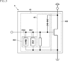
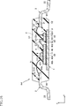
- FIG. 1 is a plan view showing a semiconductor device according to a first embodiment of the present disclosure
- FIG. FIG. 2 is a fragmentary plan view showing the semiconductor device according to the first embodiment of the present disclosure
- FIG. FIG. 3 is a circuit diagram showing a semiconductor element of the semiconductor device according to the first embodiment of the present disclosure
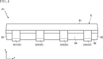
- FIG. 4 is a front view showing the semiconductor device according to the first embodiment of the present disclosure
- FIG. FIG. 5 is a side view showing the semiconductor device according to the first embodiment of the present disclosure
- FIG. FIG. 6 is a cross-sectional view along line VV in FIG.
- FIG. 7 is a cross-sectional view along line VI-VI in FIG.
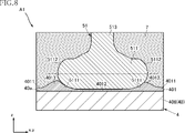
- FIG. 8 is an enlarged cross-sectional view of the main part showing the semiconductor device according to the first embodiment of the present disclosure.
- FIG. 9 is an enlarged cross-sectional view of the main part showing the semiconductor device according to the first embodiment of the present disclosure.
- FIG. 10 is a main part plan view showing a first modification of the semiconductor device according to the first embodiment of the present disclosure;
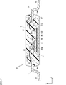
- FIG. 11 is a fragmentary plan view showing a semiconductor device according to a second embodiment of the present disclosure;
- FIG. 12 is a fragmentary plan view showing a semiconductor device according to a third embodiment of the present disclosure;
- FIG. 13 is a cross-sectional view taken along line XIII-XIII in FIG. 12.
- FIG. 14 is a cross-sectional view along line XIV-XIV in FIG. 12.
- FIG. FIG. 15 is a fragmentary plan view showing a semiconductor device according to a fourth embodiment of the present disclosure;
- FIG. 10 is a main part plan view showing a first modification of the semiconductor device according to the first embodiment of the present disclosure.
- FIG. 11 is a fragmentary plan view showing a semiconductor device according to a second embodiment of the
- FIG. 16 is a cross-sectional view taken along line XVI--XVI of FIG. 15.
- FIG. 17 is a fragmentary plan view showing a semiconductor device according to a fifth embodiment of the present disclosure; 18 is a cross-sectional view taken along line XVIII-XVIII in FIG. 17.
- FIG. 19 is a plan view of main parts showing a first modification of the semiconductor device according to the fifth embodiment of the present disclosure;
- a semiconductor device A1 of this embodiment includes a first lead 1, a plurality of second leads 2, a plurality of third leads 3, a semiconductor element 4, a plurality of first wires 51, a plurality of second wires 52, and a plurality of metal lumps. 6 , a covering portion 7 and a sealing resin 8 .
- the shape and size of the semiconductor device A1 are not particularly limited.
- An example of the size of the semiconductor device A1 is about 4 mm to 7 mm in the x direction, about 4 mm to 8 mm in the y direction, and about 0.7 mm to 2.0 mm in the z direction. be.
- FIG. 1 is a plan view showing the semiconductor device A1.
- FIG. 2 is a fragmentary plan view showing the semiconductor device A1.
- FIG. 4 is a front view showing the semiconductor device A1.
- FIG. 5 is a side view showing the semiconductor device A1.
- FIG. 6 is a cross-sectional view taken along line VI-VI of FIG.
- FIG. 7 is a cross-sectional view along line VII-VII of FIG.
- FIG. 8 is an enlarged cross-sectional view of a main part showing the semiconductor device A1.
- FIG. 9 is an enlarged cross-sectional view of a main part showing a semiconductor device A1.
- the first lead 1 is a member that supports the semiconductor element 4 and constitutes a conduction path to the semiconductor element 4 .
- the material of first lead 1 is not particularly limited, and is made of, for example, metals represented by Cu, Ni, Fe, etc., and alloys thereof.
- the first lead 1 may be formed with a plated layer made of a metal represented by Ag, Ni, Pd, Au, etc., at an appropriate position.
- the thickness of first lead 1 is not particularly limited, and is, for example, about 0.12 mm to 0.2 mm.
- the first lead 1 of this embodiment has a die pad portion 11 and two extension portions 12 .
- the die pad portion 11 is a portion that supports the semiconductor element 4 .
- the shape of the die pad portion 11 is not particularly limited, and is rectangular when viewed in the z direction in this embodiment.
- the die pad portion 11 has a die pad main surface 111 and a die pad back surface 112 .
- the die pad main surface 111 is a surface facing the z direction.
- the die pad back surface 112 is a surface facing away from the die pad main surface 111 in the thickness direction. In the illustrated example, die pad main surface 111 and die pad back surface 112 are planar.
- the two extending portions 12 are portions extending from the die pad portion 11 to both sides in the x direction.
- the extending portion 12 includes a portion extending from the die pad portion 11 along the x direction, a portion extending obliquely in the z direction toward the die pad main surface 111 with respect to the portion, and a portion extending from the portion extending in the z direction. It has a portion extending along the x-direction, and has a bent shape as a whole.
- the plurality of second leads 2 are separated from the first leads 1 and constitute a conductive path to the semiconductor element 4 .
- the plurality of second leads 2 constitute conduction paths for currents switched by the semiconductor element 4 .
- a plurality of second leads 2 are arranged on one side of the first leads 1 in the y direction. Also, the plurality of second leads 2 are arranged apart from each other in the x direction.
- the material of the second lead 2 is not particularly limited, and is made of, for example, metals represented by Cu, Ni, Fe, etc., and alloys thereof. Moreover, the second lead 2 may be formed with a plated layer made of a metal represented by Ag, Ni, Pd, Au, etc., at an appropriate position. The thickness of second lead 2 is not particularly limited, and is, for example, about 0.12 mm to 0.2 mm.
- the second lead 2 of this embodiment has a pad portion 21 and a terminal portion 22 .
- the pad portion 21 is a portion to which the first wire 51 is connected.
- the pad portion 21 is located on the side of the die pad main surface 111 facing the die pad portion 11 in the z direction.
- the terminal portion 22 is a strip-shaped portion extending outward in the y direction from the pad portion 21 .
- the terminal portion 22 has a bent shape when viewed in the x direction, and the tip portion thereof is located at substantially the same position as the die pad portion 11 in the z direction.
- the terminal portion 22 is a power terminal.
- the plurality of third leads 3 are separated from the first leads 1 and constitute a conductive path to the semiconductor element 4 .
- the plurality of third leads 3 constitute conduction paths for control signal currents for controlling the semiconductor element 4 .
- a plurality of third leads 3 are arranged on the other side in the y direction with respect to the first leads 1 . Also, the plurality of third leads 3 are arranged apart from each other in the x direction.
- the material of the third lead 3 is not particularly limited, and is made of, for example, metals represented by Cu, Ni, Fe, etc., and alloys thereof. Also, the third lead 3 may be formed with a plated layer made of a metal represented by Ag, Ni, Pd, Au, etc., at an appropriate position. The thickness of the third lead 3 is not particularly limited, and is, for example, approximately 0.12 mm to 0.2 mm.
- the third lead 3 of this embodiment has a pad portion 31 and a terminal portion 32 .
- the pad portion 31 is a portion to which the second wire 52 is connected. In the present embodiment, the pad portion 31 is located on the side of the die pad main surface 111 facing the die pad portion 11 in the z direction.
- the terminal portion 32 is a belt-like portion extending outward in the y direction from the pad portion 31 .
- the terminal portion 32 has a bent shape when viewed in the x direction, and the tip portion thereof is located at the same (or substantially the same) position as the die pad portion 11 in the z direction.
- the terminal portions 32 of the plurality of third leads 3 are distinguished from terminal portions 321, 322, 323, and 324.
- the terminal portion 321 is an output terminal and electrically connected to a third electrode 4031 which will be described later.
- the terminal portion 322 is a ground terminal and is electrically connected to a third electrode 4032 which will be described later.
- the terminal portion 323 is a self-diagnostic output terminal and electrically connected to a third electrode 4033, which will be described later.
- the terminal portion 324 is an input terminal and is electrically connected to a third electrode 4034 which will be described later.
- the semiconductor element 4 is an element that exhibits the electrical functions of the semiconductor device A1. In this embodiment, the semiconductor element 4 performs a switching function.
- the semiconductor element 4 has an element body 40 , a first electrode 401 , a second electrode 402 and a plurality of third electrodes 403 .
- the semiconductor device 4 also has a switching section 408 which constitutes a transistor that performs a switching function, and a control section 48 which controls, monitors and protects the transistor of the switching section 408 .
- the transistors included in the control unit 48 are lateral type transistors.
- the element main body 40 has an element main surface 40a and an element back surface 40b.
- the element main surface 40a faces the same side as the die pad main surface 111 in the z direction.
- the element back surface 40b is a surface that faces the side opposite to the element main surface 40a in the z direction.
- the material of the element main body 40 is not particularly limited. Examples of materials for the element body 40 include semiconductor materials such as Si, SiC, and GaN.
- the element body 40 has a switching section 408 .
- the switching unit 408 has a transistor structure typified by, for example, a MOSFET (Metal Oxide Semiconductor Field Effect Transistor), a MISFET (Metal Insulator Semiconductor Field Effect Transistor), and the like. As shown in FIGS. 1 and 2, the switching section 408 is arranged side by side with the control section 48 in the y direction when viewed in the z direction. However, the specific arrangement and the like of the switching unit 408 and the control unit 48 are not particularly limited.
- the first electrode 401 is arranged on the element main surface 40 a of the element body 40 .
- the first electrode 401 is arranged on a portion of the element main surface 40a on the side of the plurality of second leads 2 in the y direction.
- the first electrode 401 overlaps the switching section 408 when viewed in the z direction.
- the first electrode 401 is separated from the control section 48 when viewed in the z direction.
- the first electrode 401 is the source electrode.
- the material of the first electrode 401 is not particularly limited, and examples thereof include metals represented by Al (aluminum), Al—Si, Cu (copper), and alloys containing these.
- the first electrode 401 may have a structure in which layers made of a plurality of materials selected from these metals are laminated.
- the first electrode 401 of this embodiment has a base thickness portion 4011, a reduced thickness portion 4012 and a raised portion 4013.
- the base thickness portion 4011 is a portion of the first electrode 401 that occupies most of the area where the bonding portion 511 of the first wire 51 described below and the metal lump 6 are not arranged.
- the thickness of the base thickness portion 4011 is the thickness when processing such as plating for forming the first electrode 401 is completed, for example.
- the thinned portion 4012 is a portion of the first electrode 401 to which either the bonding portion 511 or the metal lump 6 is bonded, and is thinner than the base thickness portion 4011 .
- the thinned portion 4012 is a portion thinned by the bonding process of the bonding portion 511 and the metal block 6, for example.
- the raised portion 4013 is a portion located between the base thickness portion 4011 and the thinned portion 4012 .
- the raised portion 4013 annularly surrounds the reduced thickness portion 4012 .
- the raised portion 4013 is thicker than the base thickness portion 4011 and the reduced thickness portion 4012 .
- the second electrode 402 is arranged on the element back surface 40 b of the element body 40 .
- the second electrode 402 overlaps the switching section 408 and the control section 48 when viewed in the z-direction, and covers the entire surface of the element back surface 40b in this embodiment.
- the second electrode 402 is the drain electrode.
- the material of the second electrode 402 is not particularly limited, and examples thereof include metals represented by Al (aluminum), Al—Si, Cu (copper), and alloys containing these.
- the second electrode 402 may have a structure in which layers made of a plurality of materials selected from these metals are laminated.
- Control unit 48 includes, for example, a current sensor circuit, a temperature sensor circuit, an overcurrent protection circuit, an overheating protection circuit, a low voltage malfunction prevention circuit, and the like.
- the plurality of third electrodes 403 are arranged on the element main surface 40a.
- the plurality of third electrodes 403 are arranged on the portion of the element main surface 40a on the side of the plurality of third leads 3 in the y direction.
- the plurality of third electrodes 403 overlap the control section 48 when viewed in the z direction.
- the plurality of third electrodes 403 are mainly electrically connected to the controller 48 .
- the number of the multiple third electrodes 403 is not particularly limited. Also, the number of third electrodes 403 may be one.
- the semiconductor element 4 has four third electrodes 403 .
- the four third electrodes 403 include third electrodes 4031, 4032, 4033, and 4034.
- the third electrode 4031 is an output electrode, and when the load is short-circuited and a current exceeding the overcurrent detection value flows, the output current is limited.
- the third electrode 4032 is a ground electrode.
- the third electrode 4033 is a self-diagnostic output electrode and has a different potential depending on whether it is in an overcurrent or overheat state.
- the third electrode 4034 is an input electrode and internally connected to a pull-down resistor.
- FIG. 3 shows a circuit configuration example of the switching unit 408 and the control unit 48.
- the switching unit includes transistors.
- the control section 48 includes an energy absorption circuit 481 and a protection circuit 482 .
- the energy absorption circuit 481 is a circuit that absorbs electrical energy caused by transient voltage or the like, and includes, for example, a Zener diode and a resistor.
- Protection circuit 482 is a circuit that protects control unit 48 and includes, for example, heating protection unit 4821 and overcurrent protection unit 4822 .
- the plurality of first wires 51 electrically connect the first electrodes 401 of the semiconductor element 4 and the plurality of second leads 2 .
- the material of first wire 51 is not particularly limited, and is made of metal represented by Au, Cu, Al, or the like, for example.
- the first wire 51 may contain a metal different from the metal contained in the first electrode 401 .
- the first wire 51 has a bonding portion 511 , a bonding portion 512 and a loop portion 513 .
- a specific configuration of the first wire 51 is not particularly limited.
- first wire 51 is made of a material containing Cu, and is formed by a capillary, for example. In this embodiment, a current switched by the semiconductor element 4 flows through the plurality of first wires 51 .
- the semiconductor device is not limited to the configuration in which the first wire 51 is joined to the first electrode 401 .
- a conductive member made of a metal plate material other than the first wire 51 may be joined to the first electrode 401 .
- another electrode may be provided that is electrically connected to the first electrode 401 via a conductive path formed in the semiconductor element 4, and the conductive member such as the first wire 51 is in contact with this electrode.
- the bonding portion 511 is electrically connected to the first electrode 401 of the semiconductor element 4, and is arranged at a position overlapping the first electrode 401 when viewed in the z direction. In this embodiment, the bonding portion 511 is joined to the first electrode 401 and is a so-called first bonding portion.
- the bonding portion 511 has a first surface 5111 and a second surface 5112.
- the first surface 5111 and the second surface 5112 are defined by the maximum diameter portion of the bonding portion 511 (the portion having the maximum dimension in the direction perpendicular to the z direction such as the x direction and the y direction, which intersects with the dashed line shown in FIG. 8). are aligned in the z-direction with the part where the
- the first surface 5111 is a surface inclined away from the center of the bonding portion 511 in directions perpendicular to the z-direction, such as the x-direction and the y-direction, as the distance from the first electrode 401 increases in the z-direction.
- the first surface 5111 is a convex curved surface.
- the second surface 5112 is located on the opposite side of the first surface 5111 across the maximum diameter portion, and is a convex curved surface in the illustrated example.
- the bonding portion 512 is a portion that is bonded to the pad portion 21 of the second lead 2 .
- the bonding portion 512 is a so-called second bonding portion.
- the loop portion 513 is connected to the bonding portion 511 and the bonding portion 512 and is, for example, a curved portion as a whole.
- the plurality of bonding portions 511 are arranged along the outer edge of the first electrode 401 . More specifically, they are arranged along three sides included in the outer edge of the element body 40 . Also, the bonding portions 511 are arranged in a row along the outer edge of the first electrode 401 .
- the plurality of second wires 52 electrically connect the third electrodes 403 of the semiconductor element 4 and the plurality of third leads 3 .
- the material of the second wire 52 is not particularly limited, and is made of metal represented by Au, Cu, Al, or the like, for example.
- the second wire 52 has a bonding portion 521 , a bonding portion 522 and a loop portion 523 .
- a specific configuration of the second wire 52 is not particularly limited.
- the second wire 52 is formed by a capillary, for example.
- a control signal current or the like for controlling the semiconductor element 4 flows through the plurality of second wires 52 . In the example shown in FIG.
- the third electrode 4031 and the pad portion 31 of the third lead 3 having the terminal portion 321 are connected by the second wire 52 .
- the third electrode 4032 and the pad portion 31 of the third lead 3 having the terminal portion 322 are connected by the second wire 52 .
- the third electrode 4033 and the pad portion 31 of the third lead 3 having the terminal portion 323 are connected by the second wire 52 .
- the third electrode 4034 and the pad portion 31 of the third lead 3 having the terminal portion 324 are connected by the second wire 52 .
- the bonding portion 521 is joined to the second electrode 402 of the semiconductor element 4 .
- the bonding portion 521 is a so-called first bonding portion.
- the bonding portion 522 is a portion that is bonded to the pad portion 31 of the third lead 3 .
- the bonding portion 522 is a so-called second bonding portion.
- the loop portion 523 is connected to the bonding portion 521 and the bonding portion 522 and is, for example, a curved portion as a whole.
- the plurality of metal lumps 6 each contain metal and are joined to the first electrode 401 .
- a specific configuration of the metal lump 6 is not particularly limited.
- the metal lump 6 has the same configuration as the bonding portion 511 of the first wire 51 . That is, among the methods of forming the first wire 51 using a capillary, the first wire 51 is formed by cutting the wire material after the bonding portion 511 is formed.
- the metal lump 6 of this embodiment contains Cu.
- the number of metal lumps 6 is not particularly limited, and may be one. Also, the semiconductor device of the present disclosure may be configured without the metal lump 6 .
- the arrangement of the plurality of metal lumps 6 is not particularly limited.
- the plurality of metal lumps 6 are arranged inward on the side opposite to the outer edge of the first electrode 401 with respect to the bonding portion 511 .
- the plurality of metal lumps 6 are arranged in a matrix. Examples of the matrix-like arrangement of the plurality of metal lumps 6 include an arrangement in which a plurality of rows along the two directions of the x direction and the y direction intersect, and a so-called zigzag arrangement.
- the metal block 6 has a first surface 61, a second surface 62 and a projection 63.
- the first surface 61 and the second surface 62 are defined by the maximum diameter portion of the metal lump 6 (the portion having the maximum dimension in the direction perpendicular to the z direction such as the x direction and the y direction, which intersects with the dashed line shown in FIG. 8). are aligned in the z-direction with the part where the
- the first surface 61 is a surface inclined away from the center of the metal mass 6 in directions perpendicular to the z direction, such as the x direction and the y direction, as the distance from the first electrode 401 increases in the z direction.
- the first surface 61 is a convex curved surface.
- the second surface 62 is located on the opposite side of the first surface 61 across the maximum diameter portion, and is a convex curved surface in the illustrated example.
- the protrusion 63 is a portion that protrudes from the second surface 62 in the z-direction to the side opposite to the first electrode 401 .
- the projecting portion 63 is a cut portion of the wire material for forming the metal block 6 .
- the covering portion 7 is interposed between the first electrode 401 and the sealing resin 8 .
- the covering portion 7 contains a material having higher thermal conductivity than the sealing resin 8 .
- the material of the covering portion 7 is not particularly limited, and when the sealing resin 8 is made of an insulating resin, the covering portion 7 contains metal.
- the covering portion 7 may contain a metal different from the metal contained in the first electrode 401 .
- the metal forming coating portion 7 includes, for example, Ag or Cu.
- the covering portion 7 contains sintered Ag or sintered Cu.
- the coating portion 7 contains sintered Ag, it is preferable to use sintered Ag of a type that can be formed without pressure.
- the covering portion 7 is made of pressureless sintered Ag, it can be formed, for example, by discharging a material paste to be sintered Ag from a nozzle, applying the material paste, and then heating the material paste appropriately.
- the covering portion 7 is not limited to a structure containing metal, and may contain a resin having a higher thermal conductivity than the insulating resin forming the sealing resin 8, for example.
- the sealing resin 8 is made of epoxy resin
- examples of the resin forming the covering portion 7 include PC (polycarbonate), PA6 (nylon 6), PPS (polyphenylene sulfide), PBT (polybutylene terephthalate), and the like.
- the covering portion 7 may be configured by mixing these resins with a filler for increasing thermal conductivity.
- the covering part 7 contains sintered Ag and is in contact with both the first electrode 401 and the sealing resin 8 .
- the covering portion 7 is arranged inside the outer edge of the first electrode 401 when viewed in the z direction.
- the covering portion 7 is in contact with at least one of the multiple metal lumps 6 . Also, the covering portion 7 is in contact with at least one of the bonding portions 511 of the plurality of first wires 51 . Moreover, in the illustrated example, the covering portion 7 covers most of the plurality of metal lumps 6 . Moreover, in the illustrated example, the covering portion 7 covers most of the bonding portions 511 of the plurality of first wires 51 . As shown in FIG. 2, the covering portion 7 is arranged in a region surrounded by the bonding portions 511 of the plurality of first wires 51.
- the maximum thickness of the covering portion 7 is thicker than the thickness of the bonding portion 511 of the first wire 51 .
- the thickness of the covering portion 7 is thicker at the central portion than at the outer peripheral portion when viewed along the z-direction.
- the maximum thickness of the covering portion is preferably 20 ⁇ m or more, more preferably 80 ⁇ m or more, and even more preferably 160 ⁇ m or more.
- the thickness of the covering portion 7 may have a distribution including, for example, two portions having a maximum value separated from each other in the y direction and a portion having a minimum value located between the two portions.
- the covering portion 7 includes a portion located between the first electrode 401 (protruding portion 4013 ) and the first surface 5111 of the bonding portion 511 .
- the covering portion 7 has a portion that extends below the maximum diameter portion of the bonding portion 511 .
- the covering portion 7 has a portion located between the first electrode 401 (the raised portion 4013 ) and the first surface 61 of the metal lump 6 .
- the covering portion 7 has a portion that extends below the maximum diameter portion of the first surface 61 .
- the encapsulation resin 8 includes the first lead 1, the plurality of second leads 2 and the plurality of third leads 3, and the semiconductor element 4, the plurality of first wires 51, the plurality of second wires 52, and the plurality of wires. It covers the metal block 6 and the covering portion 7 .
- the encapsulating resin 8 is made of an insulating resin, and includes, for example, an epoxy resin mixed with a filler.
- the shape of the sealing resin 8 is not particularly limited.
- the sealing resin 8 has a resin main surface 81 , a resin back surface 82 , two first resin side surfaces 83 and two second resin side surfaces 84 .
- the resin main surface 81 faces the same side as the die pad main surface 111 in the z direction, and is flat, for example.
- the resin back surface 82 is a surface facing the opposite side of the resin main surface 81 in the z-direction, and is, for example, a flat surface.
- the two first resin side surfaces 83 are located between the resin main surface 81 and the resin back surface 82 in the z direction and face both sides in the x direction.
- the two second resin side surfaces 84 are located between the resin main surface 81 and the resin back surface 82 in the z direction and face both sides in the y direction.
- the semiconductor device A ⁇ b>1 includes a covering portion 7 interposed between the first electrode 401 and the sealing resin 8 .
- the covering portion 7 contains a material having higher thermal conductivity than the sealing resin 8 . Therefore, heat transfer from the first electrode 401 to the covering portion 7 is promoted, and an excessive temperature rise of the semiconductor element 4 can be suppressed. Therefore, according to the semiconductor device A1, the energy that can be absorbed by active clamping can be increased.
- the covering portion 7 contains metal
- heat transfer from the first electrode 401 can be further enhanced.
- Ag or Cu is selected as the metal contained in the covering portion 7, the thermal conductivity of the covering portion 7 can be further increased.
- the coating portion 7 contains sintered Ag or sintered Cu, the coating portion 7 having a desired shape can be formed more reliably by applying a material paste and sintering the material paste.
- the covering portion 7 contains metal
- the covering portion 7 constitutes a conductive member in contact with the first electrode 401 .
- the contact of the covering portion 7 with the bonding portion 511 of the first wire 51 constitutes a heat transfer path that allows mutual heat transfer between the covering portion 7 and the first wire 51 . Therefore, for example, the heat transmitted to the covering portion 7 can be radiated to the second lead 2 via the first wire 51 .
- the bonding strength between the first electrode 401 and the covering portion 7 may be insufficient.
- the bonding strength between the first electrode 401 and the first wire 51 and the bonding strength between the first wire 51 and the covering portion 7 are both It is higher than the bonding strength with 7. As a result, it is possible to prevent the covering portion 7 from peeling off from the first electrode 401 and the like.
- the covering portion 7 includes a portion located between the first electrode 401 (protruding portion 4013 ) and the first surface 5111 of the bonding portion 511 .
- the covering portion 7 has a portion that extends below the maximum diameter portion of the bonding portion 511 . As a result, peeling of the covering portion 7 can be further suppressed.
- the semiconductor device A1 includes a plurality of metal lumps 6.
- the thermal conductivity of metal lump 6 is higher than that of sealing resin 8 . This can further increase the energy that can be absorbed by the active clamp.
- the bonding strength between the first electrode 401 and the covering portion 7 may be insufficient.
- the metal lump 6 contains Cu
- the bonding strength between the first electrode 401 and the metal lump 6 and the bonding strength between the metal lump 6 and the covering portion 7 are both higher than the bond strength. As a result, it is possible to prevent the covering portion 7 from peeling off from the first electrode 401 and the like.
- the covering portion 7 includes a portion positioned between the first electrode 401 (protruding portion 4013 ) and the first surface 61 of the metal lump 6 .
- the covering portion 7 has a portion that extends below the maximum diameter portion of the first surface 61 . As a result, peeling of the covering portion 7 can be further suppressed.
- the bonding portions 511 of the plurality of first wires 51 are arranged along the outer edge of the first electrode 401 .
- the plurality of metal lumps 6 are arranged inside the plurality of bonding portions 511 . This prevents the nozzle for applying the material paste from interfering with the first wires 51 when the covering portion 7 is formed after the plurality of first wires 51 and the plurality of metal lumps 6 are formed. can do. In addition, it is possible to prevent the material paste of the covering portion 7 from unintentionally adhering to the first wire 51 .
- FIG. 10 shows a first modification of the semiconductor device A1.
- the semiconductor device A11 of this modified example differs from the above-described semiconductor device A1 in the area where the covering portion 7 is provided.
- the covering portion 7 is not in contact with the bonding portions 511 of the plurality of first wires 51 and is separated from the bonding portions 511 of the plurality of first wires 51 when viewed in the z direction. That is, the bonding portion 511 is covered with the sealing resin 8 instead of the covering portion 7 . Moreover, like the semiconductor device A ⁇ b>1 , the covering portion 7 covers most of the plurality of metal lumps 6 .
- the covering portion 7 is not limited to the configuration in which it is in contact with the first wire 51 , and may be in any configuration as long as it is in contact with the first electrode 401 .
- FIG. 11 shows a semiconductor device according to the second embodiment of the present disclosure.
- the semiconductor device A2 of this embodiment differs from the above-described embodiments in that it does not include a plurality of metal lumps 6.
- FIG. 11 shows a semiconductor device according to the second embodiment of the present disclosure.
- the semiconductor device A2 of this embodiment differs from the above-described embodiments in that it does not include a plurality of metal lumps 6.
- the first electrode 401 is not joined to the metal lump 6, but is joined to the bonding portions 511 of the plurality of first wires 51.
- the contact area between the covering portion 7 and the first electrode 401 is wider than the contact area of the semiconductor device A1.
- the covering portion 7 may be in contact with or separate from the bonding portions 511 of the plurality of first wires 51 .
- This embodiment can also increase the energy that can be absorbed by the active clamp.
- the semiconductor device according to the present disclosure may be configured without the plurality of metal lumps 6 .
- the semiconductor device A3 of this embodiment shows a semiconductor device according to the third embodiment of the present disclosure.
- the relationship between the first electrode 401, the plurality of first wires 51, the plurality of 6, and the covering portion 7 is different from that of the above-described embodiment.
- the covering portion 7 is interposed between the bonding portions 511 of the plurality of first wires 51 and the plurality of metal lumps 6 and the first electrode 401 . That is, the bonding portions 511 of the plurality of first wires 51 and the plurality of metal lumps 6 are formed on the covering portion 7 and are not in contact with the first electrodes 401 . The plurality of first wires 51 and the plurality of metal lumps 6 are electrically connected to the first electrode 401 via the covering portion 7 .
- the bonding process of the plurality of first wires 51 and the formation of the plurality of metal lumps 6 may be performed.
- This embodiment can also increase the energy that can be absorbed by the active clamp.
- the structure is not limited to the structure in which the covering portion 7 covers the bonding portion 511 and the metal lumps 6, but the structure is such that the bonding portion 511 and the metal lumps 6 are formed on the covering portion 7.
- the configurations of the plurality of bonding portions 511, the plurality of metal lumps 6, and the covering portion 7 in the semiconductor devices A1, A11, A2, and A3 can be arbitrarily combined and appropriately employed in the following embodiments.
- the semiconductor device A4 of this embodiment differs from the above-described embodiments mainly in the configuration of the semiconductor element 4, the semiconductor element 42, and the plurality of third wires 53. As shown in FIG.
- the semiconductor device 4 of the present embodiment has the switching section 408 of the above-described embodiment and performs a switching function, but does not have the control section 48 of the above-described embodiment.
- the semiconductor element 42 functions to control, monitor, and protect the semiconductor element 4, for example. Both the semiconductor element 4 and the semiconductor element 42 are mounted on the die pad main surface 111 of the die pad portion 11 via a bonding material 49 . In the illustrated example, the semiconductor element 4 and the semiconductor element 42 are arranged side by side in the y direction.
- the semiconductor element 42 has multiple electrodes 421 and multiple electrodes 422 .
- the plurality of electrodes 421 and the plurality of electrodes 422 are both arranged on the same side in the z direction.
- the plurality of electrodes 421 are arranged on the side where the semiconductor element 4 is located in the y direction.
- the multiple electrodes 422 are arranged on the side where the multiple third leads 3 are located in the y direction.
- the plurality of electrodes 422 includes electrodes 4221,4222,4223,4224.
- the electrode 4221 corresponds to the third electrode 4031 in the semiconductor device A1 described above.
- the electrode 4222 corresponds to the third electrode 4032 in the semiconductor device A1 described above.
- the electrode 4223 corresponds to the third electrode 4033 in the semiconductor device A1 described above.
- the electrode 4224 corresponds to the third electrode 4034 in the semiconductor device A1 described above.
- the multiple second wires 52 are individually connected to the multiple electrodes 422 of the semiconductor element 42 and the multiple third leads 3 .
- the bonding portion 521 is joined to the electrode 422 .
- the bonding portion 522 is joined to the pad portion 31 of the third lead 3 .
- the semiconductor device A4 includes a plurality of third wires 53.
- the plurality of third wires 53 are individually connected to the plurality of third electrodes 403 of the semiconductor element 4 and the plurality of electrodes 421 of the semiconductor element 42 .
- the third wire 53 has, for example, a bonding portion 531, a bonding portion 532, and a loop portion 533, and has the same configuration as the second wire 52, for example.
- the bonding portion 531 is joined to the third electrode 403 .
- the bonding portion 532 is joined to the electrode 421 .
- This embodiment can also increase the energy that can be absorbed by the active clamp.
- the specific configuration of the semiconductor element 4 is not particularly limited.
- other semiconductor elements such as the semiconductor element 42 may be mounted on the die pad portion 11 .
- the functions of the semiconductor elements other than the semiconductor element 4 are not particularly limited.
- the semiconductor device A5 of this embodiment includes a semiconductor element 4 and a semiconductor element 42, like the semiconductor device A4.
- the semiconductor element 42 is mounted on the element main surface 40a of the semiconductor element 4. As shown in FIG. That is, the semiconductor element 42 is arranged on the side opposite to the die pad section 11 with respect to the semiconductor element 4 in the z direction. The semiconductor element 4 and the semiconductor element 42 are stacked on each other.
- the semiconductor element 42 is bonded to the element main surface 40a of the semiconductor element 4 with a bonding material 49, for example.
- the semiconductor element 42 is mounted at a position separated from the first electrode 401 in the y direction when viewed in the z direction. Note that, unlike the illustrated example, the semiconductor element 42 may be arranged on the first electrode 401 .
- the first electrode 401 and the semiconductor element 42 are both rectangular with the x direction as the longitudinal direction.
- the plurality of third electrodes 403 are located between the first electrodes 401 and the semiconductor element 42 in the y direction and are arranged side by side in the x direction.
- This embodiment can also increase the energy that can be absorbed by the active clamp. Further, as understood from this embodiment, the arrangement and mounting form of the semiconductor element 42 are not particularly limited.
- FIG. 19 shows a first modification of the semiconductor device A5.
- the semiconductor device A51 of this modified example differs from the semiconductor device A5 described above mainly in the specific configurations of the semiconductor element 4 and the semiconductor element 42 .
- FIG. 19 shows a main part of the semiconductor device A51, showing a region including the semiconductor elements 4 and 42 and part of the die pad section 11, and the sealing resin 8 is omitted.
- the semiconductor device A51 may appropriately include the plurality of second leads 2 and the plurality of third leads 3 described above.
- the semiconductor element 42 is mounted on the element main surface 40 a of the semiconductor element 4 .
- the semiconductor element 42 is arranged side by side in the x direction with respect to the first electrode 401 .
- the plurality of first wires 51 in this example are formed by, for example, wedge bonding.
- the bonding portion 511 has a shape elongated in the y direction.
- a plurality of bonding portions 511 are arranged side by side in the x direction.
- the semiconductor element 42 has a long rectangular shape with the y direction as the longitudinal direction.
- the plurality of third electrodes 403 of the semiconductor element 4 are positioned on one side in the y direction with respect to the semiconductor element 42 and arranged side by side in the x direction.
- This embodiment can also increase the energy that can be absorbed by the active clamp. Further, as understood from this embodiment, the arrangement and mounting form of the semiconductor element 42 are not particularly limited.
- the semiconductor device according to the present disclosure is not limited to the above-described embodiments.
- the specific configuration of each part of the semiconductor device according to the present disclosure can be changed in various ways.
- the present disclosure includes embodiments set forth in the following appendices.
- Appendix 1 a semiconductor element having a first electrode; a sealing resin covering the semiconductor element; a covering portion; The semiconductor device, wherein the covering portion is interposed between the first electrode and the sealing resin and includes a material having higher thermal conductivity than the sealing resin.
- Appendix 2. The semiconductor device according to Appendix 1, wherein the covering portion contains metal.
- Appendix 3. The semiconductor device according to appendix 2, wherein the covering portion contains Ag or Cu.
- the semiconductor device according to any one of appendices 1 to 5, further comprising at least one first wire having a bonding portion joined to the first electrode.
- Appendix 7. the at least one first wire comprises a plurality of first wires; 7. The semiconductor device according to appendix 6, wherein the bonding portion of each of the plurality of first wires is arranged along an outer edge of the first electrode.
- Appendix 9. The semiconductor device according to any one of appendices 6 to 8, wherein each first wire contains a metal different from the metal contained in the first electrode.
- each first wire contains Cu.
- Appendix 11. The semiconductor device according to any one of appendices 6 to 10, wherein the covering portion is in contact with the bonding portion of each first wire.
- Appendix 12. The semiconductor device according to any one of appendices 6 to 11, further comprising at least one metal lump joined to the first electrode.
- Appendix 13. The semiconductor device according to appendix 12, wherein the metal lump contains a metal different from the metal contained in the first electrode.
- Appendix 14. 14.
- Appendix 15. 15. The semiconductor device according to appendix 14, wherein the covering portion covers the metal lump.
- Appendix 18. 18.
- Appendix 19 18.
- Appendix 20. 18.
- Appendix 21 21.
- Each first wire has a loop portion connected to the bonding portion, 22.
- Appendix 23 The metal lump has a first surface facing the first electrode and inclined away from the center of the metal lump as the distance from the first electrode increases, 23.
- the semiconductor device has a switching unit having a switching function and a control unit that controls the switching unit, 24.
Landscapes
- Wire Bonding (AREA)
Priority Applications (3)
| Application Number | Priority Date | Filing Date | Title |
|---|---|---|---|
| JP2023533494A JPWO2023282013A1 (https=) | 2021-07-06 | 2022-06-16 | |
| CN202280047968.2A CN117616567A (zh) | 2021-07-06 | 2022-06-16 | 半导体器件 |
| US18/533,721 US20240128169A1 (en) | 2021-07-06 | 2023-12-08 | Semiconductor device |
Applications Claiming Priority (2)
| Application Number | Priority Date | Filing Date | Title |
|---|---|---|---|
| JP2021112383 | 2021-07-06 | ||
| JP2021-112383 | 2021-07-06 |
Related Child Applications (1)
| Application Number | Title | Priority Date | Filing Date |
|---|---|---|---|
| US18/533,721 Continuation US20240128169A1 (en) | 2021-07-06 | 2023-12-08 | Semiconductor device |
Publications (1)
| Publication Number | Publication Date |
|---|---|
| WO2023282013A1 true WO2023282013A1 (ja) | 2023-01-12 |
Family
ID=84800220
Family Applications (1)
| Application Number | Title | Priority Date | Filing Date |
|---|---|---|---|
| PCT/JP2022/024140 Ceased WO2023282013A1 (ja) | 2021-07-06 | 2022-06-16 | 半導体装置 |
Country Status (4)
| Country | Link |
|---|---|
| US (1) | US20240128169A1 (https=) |
| JP (1) | JPWO2023282013A1 (https=) |
| CN (1) | CN117616567A (https=) |
| WO (1) | WO2023282013A1 (https=) |
Cited By (2)
| Publication number | Priority date | Publication date | Assignee | Title |
|---|---|---|---|---|
| WO2024171887A1 (ja) * | 2023-02-17 | 2024-08-22 | ローム株式会社 | 半導体装置および半導体装置の製造方法 |
| WO2025052798A1 (ja) * | 2023-09-06 | 2025-03-13 | ローム株式会社 | 半導体装置 |
Families Citing this family (1)
| Publication number | Priority date | Publication date | Assignee | Title |
|---|---|---|---|---|
| JP7678773B2 (ja) * | 2022-02-15 | 2025-05-16 | 三菱電機株式会社 | 半導体装置およびその製造方法 |
Citations (4)
| Publication number | Priority date | Publication date | Assignee | Title |
|---|---|---|---|---|
| JP2014179541A (ja) * | 2013-03-15 | 2014-09-25 | Renesas Electronics Corp | 半導体装置およびその製造方法 |
| JP2017147433A (ja) * | 2015-12-16 | 2017-08-24 | ローム株式会社 | 半導体装置 |
| WO2020012958A1 (ja) * | 2018-07-12 | 2020-01-16 | ローム株式会社 | 半導体素子および半導体装置 |
| WO2020136810A1 (ja) * | 2018-12-27 | 2020-07-02 | 三菱電機株式会社 | 半導体装置、半導体装置の製造方法及び電力変換装置 |
-
2022
- 2022-06-16 WO PCT/JP2022/024140 patent/WO2023282013A1/ja not_active Ceased
- 2022-06-16 CN CN202280047968.2A patent/CN117616567A/zh active Pending
- 2022-06-16 JP JP2023533494A patent/JPWO2023282013A1/ja active Pending
-
2023
- 2023-12-08 US US18/533,721 patent/US20240128169A1/en active Pending
Patent Citations (4)
| Publication number | Priority date | Publication date | Assignee | Title |
|---|---|---|---|---|
| JP2014179541A (ja) * | 2013-03-15 | 2014-09-25 | Renesas Electronics Corp | 半導体装置およびその製造方法 |
| JP2017147433A (ja) * | 2015-12-16 | 2017-08-24 | ローム株式会社 | 半導体装置 |
| WO2020012958A1 (ja) * | 2018-07-12 | 2020-01-16 | ローム株式会社 | 半導体素子および半導体装置 |
| WO2020136810A1 (ja) * | 2018-12-27 | 2020-07-02 | 三菱電機株式会社 | 半導体装置、半導体装置の製造方法及び電力変換装置 |
Cited By (2)
| Publication number | Priority date | Publication date | Assignee | Title |
|---|---|---|---|---|
| WO2024171887A1 (ja) * | 2023-02-17 | 2024-08-22 | ローム株式会社 | 半導体装置および半導体装置の製造方法 |
| WO2025052798A1 (ja) * | 2023-09-06 | 2025-03-13 | ローム株式会社 | 半導体装置 |
Also Published As
| Publication number | Publication date |
|---|---|
| CN117616567A (zh) | 2024-02-27 |
| JPWO2023282013A1 (https=) | 2023-01-12 |
| US20240128169A1 (en) | 2024-04-18 |
Similar Documents
| Publication | Publication Date | Title |
|---|---|---|
| WO2023282013A1 (ja) | 半導体装置 | |
| US8629467B2 (en) | Semiconductor device | |
| JP7137558B2 (ja) | 半導体装置 | |
| US20200273760A1 (en) | Semiconductor module | |
| US8304902B2 (en) | Semiconductor device | |
| JP3989417B2 (ja) | 電源用デバイス | |
| JP4019993B2 (ja) | 半導体装置 | |
| JP2000058820A (ja) | パワー半導体素子及びパワーモジュール | |
| JP2005129826A (ja) | パワー半導体装置 | |
| US20240030106A1 (en) | Semiconductor device | |
| US12266627B2 (en) | Semiconductor device and method for manufacturing the same | |
| WO2024101089A1 (ja) | 半導体装置 | |
| JP2006270112A (ja) | パワー半導体素子及びパワーモジュール | |
| WO2022219995A1 (ja) | 半導体装置 | |
| US20260005175A1 (en) | Semiconductor device and method for manufacturing semiconductor device | |
| US20240071877A1 (en) | Semiconductor device | |
| JP2025082486A (ja) | 半導体装置 | |
| US20250087622A1 (en) | Semiconductor device | |
| JP2005268496A (ja) | 半導体装置 | |
| JP7817192B2 (ja) | 半導体装置 | |
| WO2022209819A1 (ja) | 半導体装置および半導体装置の製造方法 | |
| WO2026042545A1 (ja) | 半導体装置 | |
| WO2024128062A1 (ja) | 半導体装置 | |
| JP2026071337A (ja) | 半導体装置 | |
| WO2025182584A1 (ja) | 半導体装置 |
Legal Events
| Date | Code | Title | Description |
|---|---|---|---|
| 121 | Ep: the epo has been informed by wipo that ep was designated in this application |
Ref document number: 22837431 Country of ref document: EP Kind code of ref document: A1 |
|
| WWE | Wipo information: entry into national phase |
Ref document number: 2023533494 Country of ref document: JP |
|
| WWE | Wipo information: entry into national phase |
Ref document number: 202280047968.2 Country of ref document: CN |
|
| NENP | Non-entry into the national phase |
Ref country code: DE |
|
| 122 | Ep: pct application non-entry in european phase |
Ref document number: 22837431 Country of ref document: EP Kind code of ref document: A1 |