WO2023281969A1 - 半導体装置 - Google Patents
半導体装置 Download PDFInfo
- Publication number
- WO2023281969A1 WO2023281969A1 PCT/JP2022/023165 JP2022023165W WO2023281969A1 WO 2023281969 A1 WO2023281969 A1 WO 2023281969A1 JP 2022023165 W JP2022023165 W JP 2022023165W WO 2023281969 A1 WO2023281969 A1 WO 2023281969A1
- Authority
- WO
- WIPO (PCT)
- Prior art keywords
- region
- insulating film
- gate
- semiconductor device
- main surface
- Prior art date
- Legal status (The legal status is an assumption and is not a legal conclusion. Google has not performed a legal analysis and makes no representation as to the accuracy of the status listed.)
- Ceased
Links
Images


Classifications
-
- H—ELECTRICITY
- H10—SEMICONDUCTOR DEVICES; ELECTRIC SOLID-STATE DEVICES NOT OTHERWISE PROVIDED FOR
- H10D—INORGANIC ELECTRIC SEMICONDUCTOR DEVICES
- H10D84/00—Integrated devices formed in or on semiconductor substrates that comprise only semiconducting layers, e.g. on Si wafers or on GaAs-on-Si wafers
- H10D84/101—Integrated devices comprising main components and built-in components, e.g. IGBT having built-in freewheel diode
- H10D84/151—LDMOS having built-in components
- H10D84/153—LDMOS having built-in components the built-in component being PN junction diodes
- H10D84/154—LDMOS having built-in components the built-in component being PN junction diodes in antiparallel diode configurations
-
- H—ELECTRICITY
- H10—SEMICONDUCTOR DEVICES; ELECTRIC SOLID-STATE DEVICES NOT OTHERWISE PROVIDED FOR
- H10D—INORGANIC ELECTRIC SEMICONDUCTOR DEVICES
- H10D64/00—Electrodes of devices having potential barriers
- H10D64/111—Field plates
-
- H—ELECTRICITY
- H10—SEMICONDUCTOR DEVICES; ELECTRIC SOLID-STATE DEVICES NOT OTHERWISE PROVIDED FOR
- H10D—INORGANIC ELECTRIC SEMICONDUCTOR DEVICES
- H10D30/00—Field-effect transistors [FET]
- H10D30/01—Manufacture or treatment
- H10D30/021—Manufacture or treatment of FETs having insulated gates [IGFET]
-
- H—ELECTRICITY
- H10—SEMICONDUCTOR DEVICES; ELECTRIC SOLID-STATE DEVICES NOT OTHERWISE PROVIDED FOR
- H10D—INORGANIC ELECTRIC SEMICONDUCTOR DEVICES
- H10D30/00—Field-effect transistors [FET]
- H10D30/60—Insulated-gate field-effect transistors [IGFET]
-
- H—ELECTRICITY
- H10—SEMICONDUCTOR DEVICES; ELECTRIC SOLID-STATE DEVICES NOT OTHERWISE PROVIDED FOR
- H10D—INORGANIC ELECTRIC SEMICONDUCTOR DEVICES
- H10D62/00—Semiconductor bodies, or regions thereof, of devices having potential barriers
- H10D62/10—Shapes, relative sizes or dispositions of the regions of the semiconductor bodies; Shapes of the semiconductor bodies
- H10D62/124—Shapes, relative sizes or dispositions of the regions of semiconductor bodies or of junctions between the regions
- H10D62/126—Top-view geometrical layouts of the regions or the junctions
-
- H—ELECTRICITY
- H10—SEMICONDUCTOR DEVICES; ELECTRIC SOLID-STATE DEVICES NOT OTHERWISE PROVIDED FOR
- H10D—INORGANIC ELECTRIC SEMICONDUCTOR DEVICES
- H10D62/00—Semiconductor bodies, or regions thereof, of devices having potential barriers
- H10D62/10—Shapes, relative sizes or dispositions of the regions of the semiconductor bodies; Shapes of the semiconductor bodies
- H10D62/13—Semiconductor regions connected to electrodes carrying current to be rectified, amplified or switched, e.g. source or drain regions
- H10D62/149—Source or drain regions of field-effect devices
- H10D62/151—Source or drain regions of field-effect devices of IGFETs
- H10D62/156—Drain regions of DMOS transistors
- H10D62/157—Impurity concentrations or distributions
-
- H—ELECTRICITY
- H10—SEMICONDUCTOR DEVICES; ELECTRIC SOLID-STATE DEVICES NOT OTHERWISE PROVIDED FOR
- H10D—INORGANIC ELECTRIC SEMICONDUCTOR DEVICES
- H10D64/00—Electrodes of devices having potential barriers
- H10D64/60—Electrodes characterised by their materials
- H10D64/66—Electrodes having a conductor capacitively coupled to a semiconductor by an insulator, e.g. MIS electrodes
- H10D64/661—Electrodes having a conductor capacitively coupled to a semiconductor by an insulator, e.g. MIS electrodes the conductor comprising a layer of silicon contacting the insulator, e.g. polysilicon having vertical doping variation
-
- H—ELECTRICITY
- H10—SEMICONDUCTOR DEVICES; ELECTRIC SOLID-STATE DEVICES NOT OTHERWISE PROVIDED FOR
- H10D—INORGANIC ELECTRIC SEMICONDUCTOR DEVICES
- H10D64/00—Electrodes of devices having potential barriers
- H10D64/60—Electrodes characterised by their materials
- H10D64/66—Electrodes having a conductor capacitively coupled to a semiconductor by an insulator, e.g. MIS electrodes
- H10D64/671—Electrodes having a conductor capacitively coupled to a semiconductor by an insulator, e.g. MIS electrodes the conductor having lateral variation in doping or structure
-
- H—ELECTRICITY
- H10—SEMICONDUCTOR DEVICES; ELECTRIC SOLID-STATE DEVICES NOT OTHERWISE PROVIDED FOR
- H10D—INORGANIC ELECTRIC SEMICONDUCTOR DEVICES
- H10D8/00—Diodes
- H10D8/50—PIN diodes
-
- H—ELECTRICITY
- H10—SEMICONDUCTOR DEVICES; ELECTRIC SOLID-STATE DEVICES NOT OTHERWISE PROVIDED FOR
- H10D—INORGANIC ELECTRIC SEMICONDUCTOR DEVICES
- H10D84/00—Integrated devices formed in or on semiconductor substrates that comprise only semiconducting layers, e.g. on Si wafers or on GaAs-on-Si wafers
- H10D84/01—Manufacture or treatment
- H10D84/0123—Integrating together multiple components covered by H10D12/00 or H10D30/00, e.g. integrating multiple IGBTs
- H10D84/0126—Integrating together multiple components covered by H10D12/00 or H10D30/00, e.g. integrating multiple IGBTs the components including insulated gates, e.g. IGFETs
-
- H—ELECTRICITY
- H10—SEMICONDUCTOR DEVICES; ELECTRIC SOLID-STATE DEVICES NOT OTHERWISE PROVIDED FOR
- H10D—INORGANIC ELECTRIC SEMICONDUCTOR DEVICES
- H10D84/00—Integrated devices formed in or on semiconductor substrates that comprise only semiconducting layers, e.g. on Si wafers or on GaAs-on-Si wafers
- H10D84/01—Manufacture or treatment
- H10D84/02—Manufacture or treatment characterised by using material-based technologies
- H10D84/03—Manufacture or treatment characterised by using material-based technologies using Group IV technology, e.g. silicon technology or silicon-carbide [SiC] technology
- H10D84/038—Manufacture or treatment characterised by using material-based technologies using Group IV technology, e.g. silicon technology or silicon-carbide [SiC] technology using silicon technology, e.g. SiGe
-
- H—ELECTRICITY
- H10—SEMICONDUCTOR DEVICES; ELECTRIC SOLID-STATE DEVICES NOT OTHERWISE PROVIDED FOR
- H10D—INORGANIC ELECTRIC SEMICONDUCTOR DEVICES
- H10D84/00—Integrated devices formed in or on semiconductor substrates that comprise only semiconducting layers, e.g. on Si wafers or on GaAs-on-Si wafers
- H10D84/101—Integrated devices comprising main components and built-in components, e.g. IGBT having built-in freewheel diode
- H10D84/151—LDMOS having built-in components
- H10D84/153—LDMOS having built-in components the built-in component being PN junction diodes
-
- H—ELECTRICITY
- H10—SEMICONDUCTOR DEVICES; ELECTRIC SOLID-STATE DEVICES NOT OTHERWISE PROVIDED FOR
- H10D—INORGANIC ELECTRIC SEMICONDUCTOR DEVICES
- H10D30/00—Field-effect transistors [FET]
- H10D30/01—Manufacture or treatment
- H10D30/021—Manufacture or treatment of FETs having insulated gates [IGFET]
- H10D30/0212—Manufacture or treatment of FETs having insulated gates [IGFET] using self-aligned silicidation
-
- H—ELECTRICITY
- H10—SEMICONDUCTOR DEVICES; ELECTRIC SOLID-STATE DEVICES NOT OTHERWISE PROVIDED FOR
- H10D—INORGANIC ELECTRIC SEMICONDUCTOR DEVICES
- H10D30/00—Field-effect transistors [FET]
- H10D30/60—Insulated-gate field-effect transistors [IGFET]
- H10D30/64—Double-diffused metal-oxide semiconductor [DMOS] FETs
- H10D30/65—Lateral DMOS [LDMOS] FETs
- H10D30/655—Lateral DMOS [LDMOS] FETs having edge termination structures
-
- H—ELECTRICITY
- H10—SEMICONDUCTOR DEVICES; ELECTRIC SOLID-STATE DEVICES NOT OTHERWISE PROVIDED FOR
- H10D—INORGANIC ELECTRIC SEMICONDUCTOR DEVICES
- H10D62/00—Semiconductor bodies, or regions thereof, of devices having potential barriers
- H10D62/10—Shapes, relative sizes or dispositions of the regions of the semiconductor bodies; Shapes of the semiconductor bodies
- H10D62/102—Constructional design considerations for preventing surface leakage or controlling electric field concentration
- H10D62/103—Constructional design considerations for preventing surface leakage or controlling electric field concentration for increasing or controlling the breakdown voltage of reverse-biased devices
- H10D62/105—Constructional design considerations for preventing surface leakage or controlling electric field concentration for increasing or controlling the breakdown voltage of reverse-biased devices by having particular doping profiles, shapes or arrangements of PN junctions; by having supplementary regions, e.g. junction termination extension [JTE]
- H10D62/106—Constructional design considerations for preventing surface leakage or controlling electric field concentration for increasing or controlling the breakdown voltage of reverse-biased devices by having particular doping profiles, shapes or arrangements of PN junctions; by having supplementary regions, e.g. junction termination extension [JTE] having supplementary regions doped oppositely to or in rectifying contact with regions of the semiconductor bodies, e.g. guard rings with PN or Schottky junctions
-
- H—ELECTRICITY
- H10—SEMICONDUCTOR DEVICES; ELECTRIC SOLID-STATE DEVICES NOT OTHERWISE PROVIDED FOR
- H10D—INORGANIC ELECTRIC SEMICONDUCTOR DEVICES
- H10D62/00—Semiconductor bodies, or regions thereof, of devices having potential barriers
- H10D62/10—Shapes, relative sizes or dispositions of the regions of the semiconductor bodies; Shapes of the semiconductor bodies
- H10D62/124—Shapes, relative sizes or dispositions of the regions of semiconductor bodies or of junctions between the regions
- H10D62/126—Top-view geometrical layouts of the regions or the junctions
- H10D62/127—Top-view geometrical layouts of the regions or the junctions of cellular field-effect devices, e.g. multicellular DMOS transistors or IGBTs
-
- H—ELECTRICITY
- H10—SEMICONDUCTOR DEVICES; ELECTRIC SOLID-STATE DEVICES NOT OTHERWISE PROVIDED FOR
- H10D—INORGANIC ELECTRIC SEMICONDUCTOR DEVICES
- H10D62/00—Semiconductor bodies, or regions thereof, of devices having potential barriers
- H10D62/10—Shapes, relative sizes or dispositions of the regions of the semiconductor bodies; Shapes of the semiconductor bodies
- H10D62/17—Semiconductor regions connected to electrodes not carrying current to be rectified, amplified or switched, e.g. channel regions
- H10D62/351—Substrate regions of field-effect devices
- H10D62/357—Substrate regions of field-effect devices of FETs
- H10D62/364—Substrate regions of field-effect devices of FETs of IGFETs
- H10D62/371—Inactive supplementary semiconductor regions, e.g. for preventing punch-through, improving capacity effect or leakage current
-
- H—ELECTRICITY
- H10—SEMICONDUCTOR DEVICES; ELECTRIC SOLID-STATE DEVICES NOT OTHERWISE PROVIDED FOR
- H10D—INORGANIC ELECTRIC SEMICONDUCTOR DEVICES
- H10D62/00—Semiconductor bodies, or regions thereof, of devices having potential barriers
- H10D62/10—Shapes, relative sizes or dispositions of the regions of the semiconductor bodies; Shapes of the semiconductor bodies
- H10D62/17—Semiconductor regions connected to electrodes not carrying current to be rectified, amplified or switched, e.g. channel regions
- H10D62/393—Body regions of DMOS transistors or IGBTs
-
- H—ELECTRICITY
- H10—SEMICONDUCTOR DEVICES; ELECTRIC SOLID-STATE DEVICES NOT OTHERWISE PROVIDED FOR
- H10D—INORGANIC ELECTRIC SEMICONDUCTOR DEVICES
- H10D64/00—Electrodes of devices having potential barriers
- H10D64/20—Electrodes characterised by their shapes, relative sizes or dispositions
- H10D64/27—Electrodes not carrying the current to be rectified, amplified, oscillated or switched, e.g. gates
- H10D64/311—Gate electrodes for field-effect devices
- H10D64/411—Gate electrodes for field-effect devices for FETs
- H10D64/511—Gate electrodes for field-effect devices for FETs for IGFETs
- H10D64/514—Gate electrodes for field-effect devices for FETs for IGFETs characterised by the insulating layers
- H10D64/516—Gate electrodes for field-effect devices for FETs for IGFETs characterised by the insulating layers the thicknesses being non-uniform
Definitions
- Patent Document 1 discloses a field effect transistor including a silicon substrate, a drift region, a channel region, a gate insulating film and a polysilicon gate.
- One embodiment provides a semiconductor device capable of improving electrical characteristics.
- a chip having a main surface, a channel region of a first conductivity type formed in a surface layer portion of the main surface, and a first conductivity type channel region formed in the surface layer portion of the main surface so as to be adjacent to the channel region.
- a chip having a main surface, a channel region of a first conductivity type formed in a surface layer portion of the main surface, and a first conductivity type channel region formed in the surface layer portion of the main surface so as to be adjacent to the channel region.
- a two-conductivity-type drift region a gate insulating film covering the channel region and the drift region on the main surface; and the gate facing the channel region and the drift region with the gate insulating film interposed therebetween.
- a polysilicon gate covering an insulating film; and a pn junction diode formed inside the polysilicon gate.
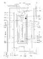
- FIG. 1 is a plan view showing the semiconductor device according to the first embodiment.
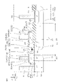
- FIG. FIG. 2 is an enlarged view of area II shown in FIG.
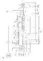
- FIG. 3 is a cross-sectional view taken along line III-III shown in FIG. 4 is an enlarged view of a main part of the structure shown in FIG. 3.
- FIG. 5 is an enlarged view of a main part showing a semiconductor device according to the first embodiment.
- FIG. 6 is an enlarged view of a main part showing a semiconductor device according to the second embodiment.
- FIG. 7 is a graph showing figures of merit.
- FIG. 8 is an enlarged view of a main part showing a semiconductor device according to a second embodiment.
- FIG. 9 is an enlarged view of a main part showing a semiconductor device according to a third embodiment.
- FIG. 10 is an enlarged view of essential parts showing a semiconductor device according to a fourth embodiment.
- FIG. 11 is an enlarged view of essential parts showing a semiconductor device according to a fifth embodiment.
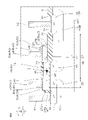
- FIG. 1 is a plan view showing a semiconductor device 1A according to the first embodiment.
- FIG. 2 is an enlarged view of area II shown in FIG.
- FIG. 3 is a cross-sectional view taken along line III-III shown in FIG. 4 is an enlarged view of a main part of the structure shown in FIG. 3.
- semiconductor device 1A includes a rectangular parallelepiped chip 2 (semiconductor chip).
- Chip 2 consists in this embodiment of a silicon chip.
- the chip 2 has a first main surface 3 on one side, a second main surface 4 on the other side, and first to fourth side surfaces 5A to 5D connecting the first main surface 3 and the second main surface 4. ing.
- the first main surface 3 and the second main surface 4 are formed in a quadrangular shape when viewed from above in the normal direction Z thereof.
- the normal direction Z is also the thickness direction of the chip 2 .
- the first side surface 5A and the second side surface 5B extend along the first direction X along the first main surface 3 and face each other along the second direction Y intersecting (specifically, perpendicular to) the first direction X. ing.
- the third side surface 5C and the fourth side surface 5D extend along the second direction Y and face each other along the first direction X. As shown in FIG.
- Semiconductor device 1 ⁇ /b>A includes an n-type first region 6 formed in a surface layer portion of first main surface 3 .
- the first region 6 is formed in layers extending along the first main surface 3 and exposed from the first main surface 3 and the first to fourth side surfaces 5A to 5D. That is, the first region 6 has the first main surface 3 and part of the first to fourth side surfaces 5A to 5D.
- the n-type impurity concentration of the first region 6 may be 1 ⁇ 10 14 cm ⁇ 3 or more and 1 ⁇ 10 16 cm ⁇ 3 or less.
- the thickness of the first region 6 may be 1 ⁇ m or more and 10 ⁇ m or less.
- the first region 6 is formed by an n-type epitaxial layer in this embodiment.
- the semiconductor device 1A includes a p-type second region 7 formed in the surface layer portion of the second main surface 4 .
- the second region 7 may also be referred to as a "base region".
- the second region 7 is formed in layers extending along the second main surface 4 and exposed from the second main surface 4 and the first to fourth side surfaces 5A to 5D. That is, the second region 7 has the second main surface 4 and part of the first to fourth side surfaces 5A to 5D.
- the second region 7 is connected to the first region 6 inside the chip 2 .
- the second region 7 may have a substantially constant p-type impurity concentration in the thickness direction.
- the p-type impurity concentration of the second region 7 may be 1 ⁇ 10 14 cm ⁇ 3 or more and 1 ⁇ 10 18 cm ⁇ 3 or less.
- the thickness of the second region 7 may be 100 ⁇ m or more and 1000 ⁇ m or less.
- the thickness of the second region 7 is adjusted by grinding the second principal surface 4 .
- the second region 7 is formed of a p-type semiconductor substrate in this embodiment. That is, the chip 2 has a laminated structure including a semiconductor substrate and an epitaxial layer. The second region 7 is formed in the semiconductor substrate and the first region 6 is formed in the epitaxial layer.
- the semiconductor device 1A includes a plurality of device regions 8 provided in the first region 6.
- a plurality of device regions 8 are partitioned inwardly of the first major surface 3 at intervals from the first to fourth side surfaces 5A to 5D in plan view.
- the number, arrangement and shape of the device regions 8 are arbitrary, and are not limited to a specific number, arrangement and shape.
- the plurality of device regions 8 each contain various functional devices. Functional devices may include at least one of semiconductor switching devices, semiconductor rectifying devices and passive devices.
- the semiconductor switching device includes at least one of BJT (Bipolar Junction Transistor), JFET (Junction Field Effect Transistor), MISFET (Metal Insulator Semiconductor Field Effect Transistor), and IGBT (Insulated Gate Bipolar Junction Transistor). good too.
- the semiconductor rectifier device may include at least one of a pn junction diode 29, a pin junction diode, a Zener diode, a Schottky barrier diode and a fast recovery diode.
- Passive devices may include at least one of resistors, capacitors, inductors and fuses.
- the plurality of device regions 8 includes at least one MIS region 9 in this form (see region II in FIG. 1).
- MIS region 9 is a region containing at least one transistor cell 10 .
- a specific structure of the MIS region 9 side will be described below.
- semiconductor device 1A includes p-type separation region 11 as an example of a region separation structure that partitions MIS region 9 on first main surface 3. )including.
- the separation region 11 is formed in an annular shape surrounding part of the first main surface 3 in plan view, and partitions the MIS region 9 having a predetermined shape.
- the isolation region 11 electrically isolates the MIS region 9 from other regions (the device region 8).
- the separation region 11 is formed in a quadrangular ring shape (specifically, a rectangular ring shape extending in the second direction Y) in a plan view, and is formed in a square shape (specifically, a rectangular shape extending in the second direction Y) by the inner edge. shape).
- the planar shape of the isolation region 11 (the planar shape of the MIS region 9) is arbitrary.
- the isolation region 11 extends like a wall from the first main surface 3 toward the second region 7 across the first region 6 and is electrically connected to the second region 7 .
- the isolation region 11 has a laminated structure including a first layer 11A and a second layer 11B in this form.
- the first layer 11A is formed at the boundary between the first region 6 and the second region 7. As shown in FIG.
- the first layer 11A is spaced from the first main surface 3 and the second main surface 4 with respect to the normal direction Z, and is electrically connected to the first region 6 and the second region 7 .
- the first layer 11A has a p-type impurity concentration higher than that of the second region 7 .
- the second layer 11B is formed in a region between the first main surface 3 and the first layer 11A in the first region 6 and electrically connected to the first layer 11A.
- the second layer 11B may have a p-type impurity concentration equal to or lower than the p-type impurity concentration of the first layer 11A.
- the number of second layers 11B (the number of layers) is arbitrary as long as they are electrically connected to the first layer 11A.
- a plurality of second layers 11B may be laminated in the region between the first main surface 3 and the first layer 11A.
- the isolation region 11 does not necessarily have a laminated structure including the first layer 11A and the second layer 11B as long as the MIS region 9 can be partitioned. may have.
- Semiconductor device 1A includes n-type buried region 12 formed inside chip 2 so as to cross the bottom of first region 6 in MIS region 9 .
- the embedded region 12 is formed at the boundary between the first region 6 and the second region 7 .
- Buried region 12 has a higher n-type impurity concentration than first region 6 .
- the buried region 12 may have an n-type impurity concentration of 1 ⁇ 10 17 cm ⁇ 3 or more and 1 ⁇ 10 19 cm ⁇ 3 or less.
- the embedded region 12 is formed with a gap from the first main surface 3 and the second main surface 4 with respect to the normal direction Z, and is electrically connected to the first region 6 and the second region 7 .
- Buried region 12 is spaced from the inner edge of isolation region 11 toward the inside of MIS region 9 , exposing a portion of second region 7 at the peripheral edge of MIS region 9 .
- the embedded region 12 is formed in a quadrangular shape (specifically, a rectangular shape extending in the second direction Y) along the inner edge of the isolation region 11 in plan view.
- Semiconductor device 1A includes p-type body region 13 formed in the surface layer portion of first region 6 in MIS region 9 .
- Body region 13 has a p-type impurity concentration higher than the n-type impurity concentration of first region 6 .
- the p-type impurity concentration of body region 13 may be 1 ⁇ 10 16 cm ⁇ 3 or more and 1 ⁇ 10 18 cm ⁇ 3 or less.
- the body region 13 is spaced inwardly from the separation region 11 in plan view. Specifically, body region 13 is formed in a region surrounded by the periphery of embedding region 12 with a space inward from the periphery of embedding region 12 in plan view. That is, the entire body region 13 faces the embedded region 12 in plan view.
- the body region 13 is formed in a belt shape extending in the second direction Y in plan view.
- the body region 13 has both ends curved outward in the second direction Y in an arc shape.
- the body region 13 is formed spaced from the bottom of the first region 6 (specifically, the embedded region 12) in the normal direction Z toward the first main surface 3 side.
- the semiconductor device 1A includes a p-type high-concentration body region 14 formed in the surface layer of the body region 13 in this embodiment.
- High-concentration body region 14 has a higher p-type impurity concentration than body region 13 .
- the high-concentration body region 14 is a region where the p-type impurity concentration is high in the surface layer portion of the body region 13 , and forms part of the body region 13 .
- the p-type impurity concentration of the high-concentration body region 14 may be 1 ⁇ 10 16 cm ⁇ 3 or more and 1 ⁇ 10 18 cm ⁇ 3 or less.
- the high-concentration body region 14 is formed in the surface layer portion of the body region 13 with a gap from the bottom portion of the body region 13 toward the first main surface 3 side, and faces the first region 6 with a portion of the body region 13 interposed therebetween. ing.
- the semiconductor device 1A includes at least one (one in this embodiment) n-type well region 15 formed in the surface layer portion of the first region 6 spaced apart from the body region 13 in the MIS region 9 .
- Well region 15 has a higher n-type impurity concentration than first region 6 .
- the well region 15 may have an n-type impurity concentration of 1 ⁇ 10 15 cm ⁇ 3 or more and 1 ⁇ 10 17 cm ⁇ 3 or less.
- the well region 15 is spaced inwardly from the isolation region 11 in plan view. Specifically, well region 15 is formed in a region surrounded by the periphery of buried region 12 with a space therebetween in plan view. That is, the entire area of the well region 15 faces the embedded region 12 in plan view. In this embodiment, well region 15 is formed in an annular shape surrounding body region 13 in plan view.
- the inner edge of the well region 15 may be formed in an oval shape or a square shape (specifically, a rectangular shape) in plan view.
- the outer edge of the well region 15 may be formed in an oval shape or a square shape (specifically, a rectangular shape) in plan view.
- the planar shape of the outer edge of well region 15 does not necessarily have to match the planar shape of the inner edge of well region 15 .
- the well region 15 integrally includes first to fourth well portions 15A to 15D.
- the first well portion 15A is spaced apart from the body region 13 on one side in the first direction X (the third side surface 5C side), and is formed in a strip shape extending in the second direction Y in plan view.
- the second well portion 15B is spaced apart from the body region 13 on the other side in the first direction X (the side of the fourth side surface 5D), and is formed in a strip shape extending in the second direction Y in plan view.
- the second well portion 15B faces the first well portion 15A with the body region 13 interposed therebetween.
- the third well portion 15C is spaced apart from the body region 13 on one side in the second direction Y (first side surface 5A side), and is formed in a strip shape extending in the first direction X in plan view.
- the third well portion 15C is connected to one ends of the first and second well portions 15A and 15B.
- the fourth well portion 15D is spaced apart from the body region 13 on the other side in the second direction Y (on the side of the second side surface 5B), and is formed in a strip shape extending in the first direction X in plan view.
- the fourth well portion 15D faces the third well portion 15C with the body region 13 interposed therebetween.
- the fourth well portion 15D is connected to the other ends of the first and second well portions 15A and 15B.
- the semiconductor device 1A includes an n-type high-concentration well region 16 selectively formed in the surface layer of the well region 15 in this embodiment.
- the high-concentration well region 16 has an n-type impurity concentration higher than that of the well region 15 .
- the high-concentration well region 16 is a region where the n-type impurity concentration is high in the surface layer portion of the well region 15 and forms part of the well region 15 .
- the n-type impurity concentration of the high-concentration well region 16 may be 1 ⁇ 10 15 cm ⁇ 3 or more and 1 ⁇ 10 17 cm ⁇ 3 or less.
- the high-concentration well region 16 is formed in the surface layer portion of the well region 15 with a gap from the bottom of the well region 15 toward the first main surface 3 side, and faces the first region 6 with a portion of the well region 15 interposed therebetween. ing.
- the high-concentration well region 16 is introduced into the surface layer portion of the well region 15 on the inner edge side (the periphery on the body region 13 side), and is introduced into the surface layer portion on the outer edge side of the well region 15 (the periphery on the isolation region 11 side). has not been introduced.
- the high-concentration well region 16 may be introduced into the surface layer portion on the outer edge side of the well region 15 (peripheral edge on the isolation region 11 side).
- the high-concentration well region 16 may be introduced in the entire surface layer portion of the well region 15 .
- Semiconductor device 1A includes at least one (in this embodiment, a plurality) n-type source regions 17 formed in the surface layer portion of body region 13 in MIS region 9 .
- Source region 17 has a higher n-type impurity concentration than first region 6 .
- the n-type impurity concentration of each source region 17 is higher than that of the well region 15 in this form.
- the n-type impurity concentration of each source region 17 is preferably higher than that of the high-concentration well region 16 .
- the n-type impurity concentration of each source region 17 may be 1 ⁇ 10 19 cm ⁇ 3 or more and 1 ⁇ 10 21 cm ⁇ 3 or less.
- the plurality of source regions 17 are formed at intervals inward from the periphery of the body region 13 in plan view, and are arranged at intervals in the second direction Y.
- the planar shape of the plurality of source regions 17 is arbitrary, and may be rectangular, hexagonal, or circular.
- the plurality of source regions 17 are formed at intervals from the bottom of the body region 13 to the first main surface 3 side with respect to the normal direction Z, and face the second region 7 with a part of the body region 13 interposed therebetween. .
- the plurality of source regions 17 may be formed deeper than the high-concentration body regions 14 or may be formed shallower than the high-concentration body regions 14 .
- the plurality of source regions 17 are electrically connected to the high-concentration body region 14 in the first direction X and face the second region 7 with a part or all of the high-concentration body region 14 interposed therebetween.
- Semiconductor device 1A includes at least one (a plurality in this embodiment) p-type contact regions 18 formed in the surface layer portion of body region 13 in MIS region 9 .
- Each contact region 18 has a higher p-type impurity concentration than body region 13 .
- the p-type impurity concentration of each contact region 18 is higher than that of the high-concentration body region 14 .
- Each contact region 18 may have a p-type impurity concentration of 1 ⁇ 10 19 cm ⁇ 3 or more and 1 ⁇ 10 21 cm ⁇ 3 or less.
- the plurality of contact regions 18 are formed at intervals inward from the periphery of the body region 13 so as to be connected to the plurality of source regions 17 in a plan view, and are arranged at intervals in the second direction Y. there is Specifically, the plurality of contact regions 18 and the plurality of source regions 17 are alternately arranged along the second direction Y so as to sandwich one source region 17 therebetween.
- the planar shape of the plurality of contact regions 18 is arbitrary, and may be rectangular, hexagonal, or circular.
- the plurality of contact regions 18 are formed at intervals from the bottom of the body region 13 toward the first main surface 3 with respect to the normal direction Z, and face the second region 7 with a part of the body region 13 interposed therebetween. .
- the plurality of contact regions 18 may be formed deeper than the high-concentration body regions 14 or may be formed shallower than the high-concentration body regions 14 .
- the plurality of contact regions 18 are electrically connected to the high-concentration body region 14 in the first direction X and face the second region 7 with a part or all of the high-concentration body region 14 interposed therebetween.
- the semiconductor device 1A includes at least one (two in this embodiment) n-type drain regions 19 formed in the surface layer portion of the well region 15 in the MIS region 9 .
- Each drain region 19 has a higher n-type impurity concentration than the well region 15 .
- the n-type impurity concentration of each drain region 19 is preferably higher than that of the high-concentration well region 16 .
- the n-type impurity concentration of each drain region 19 may be 1 ⁇ 10 19 cm ⁇ 3 or more and 1 ⁇ 10 21 cm ⁇ 3 or less.
- the n-type impurity concentration of each drain region 19 is preferably substantially equal to the n-type impurity concentration of the source region 17 .
- the plurality of drain regions 19 are spaced inwardly from the periphery of the well region 15 in plan view. Specifically, the plurality of drain regions 19 are formed in the surface layer portion of the well region 15 at intervals from the high-concentration well region 16 to the outer edge side of the well region 15 . The plurality of drain regions 19 are formed at intervals from the bottom of the body region 13 to the first main surface 3 side in the thickness direction, and face the first region 6 with a part of the well region 15 interposed therebetween. .
- the plurality of drain regions 19 includes a first drain region 19A and a second drain region 19B in this form.
- the first drain region 19A is arranged in the surface layer portion of the first well portion 15A, and is formed in a strip shape extending in the second direction Y in plan view.
- the second drain region 19B is arranged in the surface layer portion of the second well portion 15B and formed in a strip shape extending in the second direction Y in plan view.
- the drain region 19 is not formed in the third and fourth well portions 15C-15D in this form.
- the semiconductor device 1A includes a p-type channel region 20 formed in the surface layer portion of the first main surface 3 in the MIS region 9 .
- Channel region 20 is the region in which the conduction and non-conduction of drain/source current is controlled.
- Channel region 20 is formed between source region 17 and drain region 19 in a region on the source region 17 side.
- the channel region 20 is formed in a region between the first region 6 and the plurality of source regions 17 in the surface layer portion of the body region 13 (high-concentration body region 14).
- the semiconductor device 1A includes an n-type drift region 21 formed in the surface layer portion of the first main surface 3 so as to be adjacent to the channel region 20 in the MIS region 9 .
- the drift region 21 is a region serving as a current path for drain/source current.
- Drift region 21 is formed in a region on the drain region 19 side between source region 17 and drain region 19 .
- drift region 21 is formed in first region 6 and well region 15 in a region between body region 13 (high-concentration body region 14 ) and drain region 19 .
- the semiconductor device 1A includes a field insulating film 22 that selectively covers the drift region 21 on the first main surface 3 .
- Field insulating film 22 preferably includes a silicon oxide film.
- the field insulating film 22 selectively covers the inside and outside of the well region 15 in plan view, and the first openings 23 exposing the plurality of source regions 17 and the plurality of openings 23 exposing the plurality of drain regions 19 . includes a second opening 24 of the .
- the first opening 23 has a wall portion located on the inner edge of the well region 15 (high-concentration well region 16), and the inner edge of the well region 15 (high-concentration well region 16) and the first region 6 , body region 13 (heavy body region 14), a plurality of source regions 17 and a plurality of contact regions 18 are exposed.
- the plurality of second openings 24 each have a wall portion located on the peripheral edge portion of the corresponding drain region 19, and expose the corresponding drain region 19 in a one-to-one correspondence.
- Semiconductor device 1A includes planar gate structure 25 formed on first main surface 3 to cover channel region 20 and drift region 21 in MIS region 9 .
- Planar gate structure 25 is configured to control inversion and non-inversion of channel region 20 .
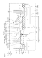
- the planar gate structure 25 has a laminated structure including a gate insulating film 26 and a poly-gate 27 (poly-gate).
- the gate insulating film 26 preferably contains a silicon oxide film.
- Polygate 27 is a gate electrode comprising conductive polysilicon. Poly gate 27 may be referred to as a "polysilicon gate.”
- the gate insulating film 26 has a thickness less than the thickness of the field insulating film 22 .
- Gate insulating film 26 covers channel region 20 and drift region 21 in first opening 23 of field insulating film 22 and continues to field insulating film 22 .
- the gate insulating film 26 includes the inner edge of the well region 15 (high-concentration well region 16), the first region 6, the body region 13 (high-concentration body region 14), the plurality of source regions 17, and the plurality of contact regions. 18 is covered.
- gate insulating film 26 is formed in an annular shape surrounding the inner portion of body region 13 in plan view.
- the poly gate 27 is formed on the gate insulating film 26 and faces the channel region 20 and the drift region 21 with the gate insulating film 26 interposed therebetween. Specifically, the poly gate 27 includes the inner edge of the well region 15 (high-concentration well region 16 ), the first region 6 , the body region 13 (high-concentration body region 14 ), and the plurality of source regions 17 with the gate insulating film 26 interposed therebetween. and a plurality of contact regions 18 . In this embodiment, poly gate 27 is formed in an annular shape surrounding the inner portion of body region 13 in plan view.
- the poly gate 27 has an inner wall 27A on the body region 13 side and an outer wall 27B on the well region 15 side.
- the inner wall 27A is arranged above the body region 13 .
- the inner wall 27A may be formed in an elliptical or rectangular shape extending along the periphery of the body region 13 .
- Inner wall 27 ⁇ /b>A defines an opening that exposes multiple source regions 17 and multiple contact regions 18 on the inner side of body region 13 .
- the outer wall 27B is arranged on the well region 15.
- the outer wall 27B is arranged in a region between the inner edge of the well region 15 and the plurality of drain regions 19 in plan view.
- the outer wall 27B is preferably arranged in a region between the heavily doped well region 16 and the plurality of drain regions 19 .
- the outer wall 27B may be formed in an elliptical or rectangular shape extending along the outer edge (inner edge) of the well region 15 .
- the planar shape of the outer wall 27B does not necessarily have to match the planar shape of the inner wall 27A.
- the poly gate 27 in this embodiment includes a lead portion 28 that extends from above the gate insulating film 26 to above the field insulating film 22 .
- the drawer portion 28 forms an outer wall 27B. That is, the outer wall 27B of the poly gate 27 is arranged on the field insulating film 22.
- the lead-out portion 28 is formed spaced from the plurality of drain regions 19 side to the inner edge side of the well region 15 in plan view, and faces the drift region 21 (well region 15 ) with the field insulating film 22 interposed therebetween.
- the lead-out portion 28 does not face the plurality of drain regions 19 .
- the semiconductor device 1A includes a pn junction diode 29 formed inside a polygate 27 (polysilicon of gate electrode).
- a pn junction diode 29 may be considered a component of the poly gate 27 .
- the pn junction diode 29 has a pn junction 30 (barrier) between the inner wall 27A and the outer wall 27B of the poly gate 27, and carrier movement from the inner wall 27A (source region 17) side toward the outer wall 27B (drain region 19) side. is configured to limit
- pn junction diode 29 is configured to restrict carrier movement from the portion of poly gate 27 located over channel region 20 to the portion of poly gate 27 located over drift region 21 . ing. In other words, pn junction diode 29 electrically isolates the portion overlying channel region 20 from the portion overlying drift region 21 with respect to poly gate 27 .
- the pn junction diode 29 is configured such that the potential difference between the inner wall 27A and the outer wall 27B inside the poly gate 27 is less than the forward threshold voltage Vdth of the pn junction 30.
- Both the first polar portion 41 and the second polar portion 42 may be considered components of the poly gate 27 .
- the first polarity portion 41 faces the channel region 20 with the gate insulating film 26 interposed therebetween.
- the second polarity portion 42 faces the drift region 21 with the gate insulating film 26 interposed therebetween, and forms the first polarity portion 41 and the pn junction 30 within the poly gate 27 .
- the pn junction diode 29 has an n-type first polarity portion 41 on the p-type channel region 20 having the opposite polarity to the channel region 20 , and has the n-type drift region 21 on the n-type drift region 21 .
- 21 has a p-type second polarity portion 42 having a polarity opposite to that of 21 .
- a first potential V1 cathode potential here
- a second potential V2 anode potential here
- a potential (V2 ⁇ Vg) other than the gate potential Vg is applied to the second polarity portion 42 . That is, first polarity portion 41 functions as the primary gate electrode controlling channel region 20 within poly gate 27 .
- a predetermined potential difference V12 is applied between the first polar portion 41 and the second polar portion 42 .
- the predetermined potential difference V12 is set to a value less than the forward threshold voltage Vdth of the pn junction diode 29 (V12 ⁇ Vdth).
- a floating potential, a reference potential, or a ground potential is exemplified as the second potential V2.
- a floating potential is a potential that naturally occurs in the second polar portion 42 in an electrically open state. That is, the state in which the floating potential is applied to the second polar portion 42 means that the second polar portion 42 is formed in an electrically floating state.
- the reference potential is a potential that serves as a reference for circuit operation.
- the reference potential may be the ground potential, or may be a potential other than the ground potential.
- such a structure restricts carrier movement from the first polarity portion 41 to the second polarity portion 42 .
- the gate threshold voltage Vgth of the poly gate 27 decreases.
- the gate threshold voltage Vgth can be adjusted by adjusting the layout of the first polar portion 41 and the second polar portion 42 . In general, a low gate threshold voltage Vgth is preferred.
- the first polar portion 41 extends from above the channel region 20 to above the drift region 21 and faces the channel region 20 and the drift region 21 with the gate insulating film 26 interposed therebetween.
- the first polar portion 41 is formed only on the gate insulating film 26 .
- the first polar portion 41 is formed in an annular shape extending along the inner wall 27A of the poly gate 27 in plan view.
- the first polar portion 41 is exposed from the inner wall 27A of the poly gate 27.
- the outer edge of the first polar portion 41 may be formed in an oval shape or a square shape (specifically, a rectangular shape) in plan view.
- the planar shape of the outer edge of the first polar portion 41 does not necessarily have to match the planar shape of the inner edge of the first polar portion 41 .
- the second polarity portion 42 is formed in a region outside the channel region 20 in plan view, and faces the drift region 21 with the gate insulating film 26 interposed therebetween. Second polarity portion 42 is further pulled out from above gate insulating film 26 onto field insulating film 22 and faces drift region 21 with gate insulating film 26 and field insulating film 22 interposed therebetween. The second polarity portion 42 does not face the channel region 20 with the gate insulating film 26 interposed therebetween.
- the second polar portion 42 is formed in an annular shape extending along the first polar portion 41 in plan view. Second polar portion 42 is exposed from outer wall 27B of poly gate 27 .
- the inner edge of the second polar portion 42 is adjusted according to the planar shape of the outer edge of the first polar portion 41, and may be formed in an oval shape or a square shape (specifically, a rectangular shape) in plan view.
- the planar shape of the outer edge of the second polar portion 42 does not necessarily have to match the planar shape of the inner edge of the second polar portion 42 .
- the second polar portion 42 and the first polar portion 41 form a pn junction 30 extending annularly in plan view.
- pn junction 30 is formed in a region outside body region 13 and surrounds body region 13 in plan view.
- pn junction 30 is preferably located in a region between the peripheral edge of body region 13 and the outer edge of gate insulating film 26 (the inner wall of field insulating film 22) in plan view.
- the pn junction 30 faces the drift region 21 across the body region 13 and does not face the channel region 20 .
- the pn junction 30 may face the first region 6 with the gate insulating film 26 interposed therebetween, or may face the well region 15 (high-concentration well region 16) with the gate insulating film 26 interposed therebetween. .
- the pn junction 30 may be arranged on the field insulating film 22 .
- the volume of the first polarity portion 41 increases, and the carrier charging speed (response speed of the transistor) for the first polarity portion 41 decreases. Therefore, it is preferable that the pn junction 30 is located on the gate insulating film 26 .
- the first polar portion 41 has a concentration gradient in which the n-type impurity concentration decreases from the inner wall 27A side of the poly gate 27 toward the outer wall 27B side.
- the first polar portion 41 includes an n-type first high concentration portion 41A and an n-type first low concentration portion 41B.
- the first high concentration portion 41A has a relatively high n-type impurity concentration and is formed on the inner wall 27A side of the poly gate 27 .
- the first high-concentration portion 41A is formed in an annular shape extending along the inner wall 27A of the poly gate 27 in plan view.
- the outer edge of the first high-density portion 41A may be formed in an oval shape or a square shape (specifically, a rectangular shape) in plan view.
- the first high-concentration portion 41A preferably extends from above the channel region 20 to above the drift region 21 and faces the channel region 20 and the drift region 21 with the gate insulating film 26 interposed therebetween.
- the first high-concentration portion 41A preferably faces the first region 6 and the body region 13 (high-concentration body region 14) with the gate insulating film 26 interposed therebetween.
- the first low concentration portion 41B has an n-type impurity concentration lower than that of the first high concentration portion 41A, and is formed on the outer wall 27B side of the poly gate 27 with respect to the first high concentration portion 41A.
- the first low-density portion 41B is formed in an annular shape extending along the first high-density portion 41A in plan view.
- the outer edge of the first low-density portion 41B may be formed in an oval shape or a square shape (specifically, a rectangular shape) in plan view.
- the planar shape of the outer edge of the first low-concentration portion 41 ⁇ /b>B does not necessarily have to match the planar shape of the inner edge of the second polar portion 42 .
- the first low-concentration portion 41B is preferably located on the gate insulating film 26 and faces the drift region 21 with the gate insulating film 26 interposed therebetween.
- the first low-concentration portion 41B is preferably located in a region between the peripheral edge of the body region 13 and the outer edge portion of the gate insulating film 26 (the inner wall portion of the field insulating film 22) in plan view.
- the first low-concentration portion 41B preferably faces at least one of the first region 6 and the well region 15 (high-concentration well region 16) with the gate insulating film 26 interposed therebetween.
- the first low-density portion 41B preferably has a width equal to or less than the width of the first high-density portion 41A (preferably less than the width of the first high-density portion 41A) in plan view.
- the width of the first high-density portion 41A and the width of the first low-density portion 41B are widths in a direction perpendicular to their extending direction in plan view.
- the plane area (volume) of the first low concentration portion 41B within the poly gate 27 (first polarity portion 41) is equal to the plane area (volume) of the first high concentration portion 41A within the poly gate 27 (first polarity portion 41). It is preferably less than
- the n-type impurity concentration of the first high concentration portion 41A may be 1 ⁇ 10 19 cm ⁇ 3 or more and 1 ⁇ 10 21 cm ⁇ 3 or less.
- the n-type impurity concentration of the first low concentration portion 41B may be 1 ⁇ 10 16 cm ⁇ 3 or more and 1 ⁇ 10 18 cm ⁇ 3 or less.
- First polar portion 41 (first high-concentration portion 41A) may contain the same n-type impurity (pentavalent element) as the n-type impurity (pentavalent element) of source region 17 .
- the first polarity portion 41 (first high concentration portion 41A) may have an n-type impurity concentration substantially equal to the n-type impurity concentration of the source region 17 . According to this structure, the first polar portion 41 can be formed using the step of forming the source region 17 .
- the second polarity portion 42 has a concentration gradient in which the p-type impurity concentration decreases from the outer wall 27B side of the poly gate 27 toward the inner wall 27A side.
- the second polar portion 42 includes a p-type second high concentration portion 42A and a p-type second low concentration portion 42B.
- the second high-concentration portion 42A has a relatively high p-type impurity concentration and is formed on the outer wall 27B side of the poly gate 27 .
- the second high concentration portion 42A is formed in an annular shape extending along the outer wall 27B of the poly gate 27 in plan view.
- the inner edge of the second high-density portion 42A may be formed in an oval shape or a square shape (specifically, a rectangular shape) in plan view.
- the second high-concentration portion 42A preferably extends from above the gate insulating film 26 onto the field insulating film 22 and faces the drift region 21 with the gate insulating film 26 and the field insulating film 22 interposed therebetween.
- the second high-concentration portion 42A preferably faces the high-concentration well region 16 with the gate insulating film 26 interposed therebetween, and faces the well region 15 with the field insulating film 22 interposed therebetween.
- the second low concentration portion 42B has a p-type impurity concentration lower than that of the second high concentration portion 42A, and is formed on the inner wall 27A side of the poly gate 27 with respect to the second high concentration portion 42A.
- the second low-density portion 42B is interposed between the first low-density portion 41B and the second high-density portion 42A, and has an annular shape extending along the first low-density portion 41B in plan view.
- the inner edge of the second low-density portion 42B is adjusted according to the planar shape of the inner edge of the first low-density portion 41B, and may be formed in an oval shape or a square shape (specifically, a rectangular shape) in plan view. .
- the planar shape of the inner edge of the second low concentration portion 42B does not necessarily have to match the planar shape of the inner edge of the second high concentration portion 42A.
- the second low concentration portion 42B forms a pn junction 30 with the first low concentration portion 41B.
- the second low-concentration portion 42B is preferably located on the gate insulating film 26 and faces the drift region 21 with the gate insulating film 26 interposed therebetween.
- the second low concentration portion 42B preferably faces at least one of the first region 6 and the well region 15 (high concentration well region 16) with the gate insulating film 26 interposed therebetween.
- the second low-density portion 42B preferably has a width equal to or less than the width of the second high-density portion 42A (preferably less than the width of the second high-density portion 42A) in plan view.
- the width of the second high-density portion 42A and the width of the second low-density portion 42B are widths in a direction orthogonal to their extending direction in plan view.
- the plane area (volume) of the second low concentration portion 42B within the poly gate 27 (second polarity portion 42) is equal to the plane area (volume) of the second high concentration portion 42A within the poly gate 27 (second polarity portion 42). It is preferably less than
- the n-type impurity concentration of the second high concentration portion 42A may be 1 ⁇ 10 19 cm ⁇ 3 or more and 1 ⁇ 10 21 cm ⁇ 3 or less.
- the n-type impurity concentration of the second low concentration portion 42B may be 1 ⁇ 10 16 cm ⁇ 3 or more and 1 ⁇ 10 18 cm ⁇ 3 or less.
- the second polar portion 42 (second high concentration portion 42A) may contain the same p-type impurity (trivalent element) as the p-type impurity (trivalent element) of the contact region 18 .
- the second polarity portion 42 (second high concentration portion 42A) may have a p-type impurity concentration substantially equal to the p-type impurity concentration of the contact region 18 . According to this structure, the second polarity portion 42 can be formed using the step of forming the contact region 18 .
- the semiconductor device 1A includes a cap insulating film 45 that selectively covers the main surface of the poly gate 27 .
- the cap insulating film 45 preferably contains silicon oxide.
- Cap insulating film 45 selectively covers the main surface of poly gate 27 so as to cover pn junction 30 . That is, the cap insulating film 45 covers the first polar portion 41 and the second polar portion 42 .
- the cap insulating film 45 has a removed portion 46 exposing the main surface of the poly gate 27 other than the pn junction 30 .
- the removal section 46 includes a first removal section 46A and a second removal section 46B in this embodiment.
- the first removed portion 46A exposes the first polar portion 41 .
- the first removed portion 46A preferably exposes at least the first high-density portion 41A.
- the first removed portion 46A may expose both the first high concentration portion 41A and the first low concentration portion 41B.
- the first removed portion 46A may be formed in an annular shape extending along the first polar portion 41 in plan view. Of course, a plurality of first removed portions 46A may be formed along the first polar portion 41 at intervals.
- the second removed portion 46B exposes the second polar portion 42 .
- the second removed portion 46B preferably exposes at least the second high-density portion 42A.
- the second removed portion 46B may expose both the second high concentration portion 42A and the second low concentration portion 42B.
- the second removed portion 46B may be formed in an annular shape extending along the second polar portion 42 in plan view. Of course, a plurality of second removed portions 46B may be formed along the second polar portion 42 at intervals.
- the semiconductor device 1A includes sidewall insulating films 47 that cover the sidewalls of the poly gate 27 .
- Sidewall insulating film 47 preferably includes one or both of a silicon oxide film and a silicon nitride film.
- Sidewall insulating film 47 includes a first sidewall insulating film 47A and a second sidewall insulating film 47B.
- the first sidewall insulating film 47A covers the inner wall 27A of the poly gate 27. As shown in FIG.
- the first sidewall insulating film 47A covers the first polar portion 41 (first high-concentration portion 41A) exposed from the inner wall 27A.
- the second sidewall insulating film 47B covers the outer wall 27B of the poly gate 27. As shown in FIG. Specifically, the second sidewall insulating film 47B covers the second polar portion 42 (second high concentration portion 42A) exposed from the outer wall 27B.
- the semiconductor device 1A includes source silicide 48 formed on the surface layer of the source region 17 .
- the source silicide 48 is a film-like region in which silicon located in the surface layer of the source region 17 and the surface layer of the contact region 18 is silicided with metal.
- the source silicide 48 contains the n-type impurity (pentavalent element) of the source region 17 and the p-type impurity (trivalent element) of the contact region 18 .
- the metal used for the silicide may be titanium, nickel, chromium, cobalt, tungsten, molybdenum, etc. (the same applies below).
- the semiconductor device 1A includes a plurality of drain silicides 49 respectively formed on the surface layer portions of the plurality of drain regions 19 .
- Each drain silicide 49 is a film-like region in which silicon located in the surface layer of each drain region 19 is silicided with a metal.
- Each drain silicide 49 contains the n-type impurity (pentavalent element) of each drain region 19 .
- the semiconductor device 1A includes a gate silicide 50 formed in a portion exposed from the removed portion 46 on the main surface of the poly gate 27 .
- Gate silicide 50 may be referred to as "gate polycide.”
- the gate silicide 50 includes a first gate silicide 50A and a second gate silicide 50B.
- the first gate silicide 50A is formed in the first polarity portion 41 (first high concentration portion 41A) exposed from the first removed portion 46A on the main surface of the poly gate 27.
- the first gate silicide 50A is a film-like region in which the polysilicon of the surface layer of the first polarity portion 41 is polycidated (silicided) with a metal.
- the first gate silicide 50A contains the n-type impurity (pentavalent element) of the first polar portion 41 .
- the main surface of the first gate silicide 50A may be located on the chip 2 side (gate insulating film 26 side) with respect to the main surface of the cap insulating film 45 .
- the second gate silicide 50B is formed in the second polarity portion 42 (second high concentration portion 42A) exposed from the second removal portion 46B on the main surface of the poly gate 27.
- the second gate silicide 50B is a film-like region formed by polysiliconizing (siliciding) the polysilicon of the surface layer of the second polarity portion 42 with a metal.
- the second gate silicide 50B contains the p-type impurity (trivalent element) of the second polarity portion 42.
- the main surface of the second gate silicide 50B may have a portion located on the chip 2 side (gate insulating film 26 side) with respect to the main surface of the cap insulating film 45 .
- the main surface of the second gate silicide 50B may have a portion that protrudes above the main surface of the cap insulating film 45 (on the side opposite to the chip 2) above the field insulating film 22.
- the semiconductor device 1A includes at least one source contact electrode 51.
- Source contact electrode 51 is electrically connected to multiple source regions 17 and multiple contact regions 18 via source silicide 48 on first main surface 3 .
- Source contact electrode 51 applies source potential Vs to source region 17 and contact region 18 .
- the semiconductor device 1A includes a plurality of drain contact electrodes 52.
- the multiple drain contact electrodes 52 are electrically connected to the multiple drain regions 19 via the drain silicide 49 on the first main surface 3 .
- the drain contact electrode 52 applies the drain potential Vd to the drain region 19 .
- the semiconductor device 1A includes a plurality of gate contact electrodes 53.
- a plurality of gate contact electrodes 53 are disposed over the poly gate 27 and electrically connected to the poly gate 27 through the gate silicide 50 .
- the plurality of gate contact electrodes 53 includes at least one (plurality in this embodiment) first gate contact electrode 53A and at least one (plurality in this embodiment) second gate contact electrode 53B. .
- the first gate contact electrode 53A is electrically connected to the first polarity portion 41 through the first gate silicide 50A.
- the first gate contact electrode 53A applies the first potential V1 (gate potential Vg) to the first polarity portion 41 .
- the plurality of first gate contact electrodes 53A may be connected to portions located at both end portions in the second direction Y of the first polarity portion 41, respectively.
- the plurality of first gate contact electrodes 53A are preferably connected to the first high concentration portion 41A.
- the second gate contact electrode 53B is electrically connected to the second polarity portion 42 via the second gate silicide 50B.
- the second gate contact electrode 53B applies a second potential V2 different from the first potential V1 to the second polarity portion 42 .
- the second potential V2 is exemplified by a floating potential, a reference potential, or a ground potential.
- the plurality of second gate contact electrodes 53B may be connected to portions located at both end portions in the second direction Y of the second polarity portion 42, respectively.
- the plurality of second gate contact electrodes 53B are preferably connected to the second high concentration portion 42A.
- transistor cell 10 includes channel region 20 , drift region 21 and planar gate structure 25 .
- the transistor cell 10 is configured to conduct a drain/source current during ON operation.
- a source potential Vs is applied to the source region 17
- a drain potential Vd is applied to the drain region 19
- a gate potential Vg is applied to the poly gate 27 .
- FIG. 5 corresponds to FIG. 4 and is an enlarged view of a main part showing a semiconductor device 61 according to the first embodiment.
- semiconductor device 61 includes poly gate 62 of a single conductivity type (n type in this embodiment) instead of poly gate 27 .
- Semiconductor device 61 may include p-type poly gate 62 instead of n-type poly gate 62 .
- Semiconductor device 61 does not include pn junction diode 29 inside poly gate 62 .
- FIG. 6 corresponds to FIG. 4 and is an enlarged view of a main part showing a semiconductor device 63 according to the second embodiment.
- semiconductor device 63 includes a single-conductivity-type (n-type in this embodiment) polygate 62 and does not include pn junction diode 29 inside polygate 62 , like semiconductor device 61 .
- the semiconductor device 63 may include a p-type polygate 62 instead of the n-type polygate 62 .
- Semiconductor device 63 includes a gate removal portion 64 that separates poly gate 62 into a plurality of portions. The poly gate 62 is separated by a gate removal portion 64 into a first poly gate 62A on the channel region 20 side and a second poly gate 62B on the drift region 21 side.
- the first poly gate 62A is arranged only on the gate insulating film 26 in this form, and faces the channel region 20 and the drift region 21 with the gate insulating film 26 interposed therebetween.
- the second poly gate 62B extends from above the gate insulating film 26 onto the field insulating film 22 and faces the drift region 21 with the gate insulating film 26 and the field insulating film 22 interposed therebetween.
- Cap insulating film 45 is interposed between first polygate 62A and second polygate 62B to electrically insulate first polygate 62A and second polygate 62B.
- the gate silicide 50 covers the main surface of the first polygate 62A and the main surface of the second polygate 62B. At least one gate contact electrode 53 is electrically connected through the gate silicide 50 to the first poly gate 62A, and at least one gate contact electrode 53 is electrically connected through the gate silicide 50 to the second poly gate 62B.
- a gate potential Vg is applied to the first polygate 62A, and a floating potential or source potential Vs is applied to the second polygate 62B.
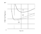
- Fig. 7 is a graph showing the figure of merit (FOM).
- the vertical axis indicates the figure of merit FOM [au] of the transistor cell 10 and the horizontal axis indicates the gate/source voltage Vgs [V] of the transistor cell 10 .
- the amount of charge Qgd includes the amount of charge between poly gate 62 and drift region 21 .
- a smaller value of the figure of merit FOM means that the performance of the transistor cell 10 is higher.
- FIG. 7 shows the first characteristic S1, the second characteristic S2 and the third characteristic OM.
- a first characteristic S1 indicates the figure of merit FOM of the semiconductor device 61 according to the first reference embodiment.
- a second characteristic S2 indicates the figure of merit FOM of the semiconductor device 63 according to the second reference embodiment.
- a third characteristic S3 indicates the figure of merit FOM of the semiconductor device 1A according to the first embodiment.
- the figure of merit FOM for the semiconductor device 63 is superior to the figure of merit FOM for the semiconductor device 61, and the figure of merit FOM for the semiconductor device 1A is superior to the performance of the semiconductor device 63. Better than exponential FOM.
- the amount of charge Qgd increases due to the single-conductivity-type poly gate 62 having a relatively large volume.
- the poly gate 62 is physically separated into a first poly gate 62 A on the channel region 20 side and a second poly gate 62 B on the drift region 21 side by the gate removal portion 64 .
- a first poly gate 62 A with a relatively small volume functions as a gate electrode controlling the channel region 20 . Therefore, the on-resistance Ron increases as a counterbalance to the decrease in the amount of charge Qgd.
- the poly gate 62 has a gate removal portion 64 electrically insulated from the gate voltage, there is an area where the gate voltage is insufficiently applied in the drift region 21 . As a result, a region in which the on-resistance Ron increases occurs in the drift region 21 .
- the poly gate 27 is electrically separated into a portion located on the channel region 20 and a portion located on the drift region 21 by the pn junction 30 (pn junction diode 29).
- the poly gate 27 has a first polarity portion 41 facing the channel region 20 with the gate insulating film 26 interposed therebetween and a second polarity portion 42 facing the drift region 21 with the gate insulating film 26 interposed therebetween.
- the pn junction 30 restricts the movement of carriers from the portion of the poly gate 27 located over the channel region 20 to the portion of the poly gate 27 located over the drift region 21 .
- the portion of the poly gate 27 that functions as the gate electrode that is, the first polarity portion 41
- the pn junction 30 restricts the movement of carriers from the portion of the poly gate 27 located over the channel region 20 to the portion of the poly gate 27 located over the drift region 21 .
- the charge amount Qgd can be reduced.
- the poly gate 27 does not have a physically disconnected portion (the gate removal portion 64), so that the gate voltage is appropriately applied to the drift region 21. be able to. Thereby, an increase in the on-resistance Ron in the drift region 21 can be suppressed. Therefore, according to the semiconductor device 1A, compared with the semiconductor devices 61 and 63, the figure of merit FOM can be improved.
- the semiconductor device 1A includes the chip 2, the p-type (first conductivity type) channel region 20, the n-type (second conductivity type) drift region 21, and the gate insulating film 26. and poly gate 27 (polysilicon gate).
- the chip 2 has a first main surface 3 (main surface).
- Channel region 20 is formed in the surface layer portion of first main surface 3 .
- Drift region 21 is formed adjacent to channel region 20 in the surface layer portion of first main surface 3 .
- Gate insulating film 26 covers channel region 20 and drift region 21 on first main surface 3 .
- a poly gate 27 is arranged on the gate insulating film 26 .
- the poly gate 27 includes an n-type first polarity portion 41 (first portion) and a p-type second polarity portion 42 (second portion).
- the first polarity portion 41 faces the channel region 20 with the gate insulating film 26 interposed therebetween.
- the second polarity portion 42 faces the drift region 21 with the gate insulating film 26 interposed therebetween to form the first polarity portion 41 and the pn junction 30 . According to this structure, it is possible to provide the semiconductor device 1A capable of improving electrical characteristics.
- a semiconductor device 1A includes a chip 2, a p-type (first conductivity type) channel region 20, an n-type (second conductivity type) drift region 21, a gate insulating film 26, a poly gate 27 (polysilicon gate) and pn junction diode 29 .
- the chip 2 has a first main surface 3 (main surface).
- Channel region 20 is formed in the surface layer portion of first main surface 3 .
- Drift region 21 is formed adjacent to channel region 20 in the surface layer portion of first main surface 3 .
- Gate insulating film 26 covers channel region 20 and drift region 21 on first main surface 3 .
- the poly gate 27 covers the gate insulating film 26 so as to face the channel region 20 and the drift region 21 with the gate insulating film 26 interposed therebetween.
- a pn junction diode 29 is formed inside the poly gate 27 .
- P-n junction diode 29 is configured to restrict carrier movement from the portion of poly gate 27 located over channel region 20 to the portion of poly gate 27 located over drift region 21 . According to this structure, it is possible to provide the semiconductor device 1A capable of improving electrical characteristics.
- FIG. 8 corresponds to FIG. 4 and is an enlarged view of a main part showing a semiconductor device 1B according to the second embodiment.
- the semiconductor device 1B is a device having the same effect as the semiconductor device 1A.
- the semiconductor device 1A described above has a first polar portion 41 having a first high concentration portion 41A and a first low concentration portion 41B, and a second polar portion 42 having a second high concentration portion 42A and a second low concentration portion 42B. including.
- the semiconductor device 1B includes a first polar portion 41 having a uniform n impurity concentration and a second polar portion 42 having a uniform p-type impurity concentration.
- the n-type impurity concentration of the first polarity portion 41 may be adjusted to the n-type impurity concentration of the first high concentration portion 41A or the n-type impurity concentration of the first low concentration portion 41B.
- the n-type impurity concentration of the second polarity portion 42 may be adjusted to the p-type impurity concentration of the second high concentration portion 42A or the p-type impurity concentration of the second low concentration portion 42B.
- first polar portion 41 may have the first high concentration portion 41A and the first low concentration portion 41B, while the second polar portion 42 may have a uniform p-type impurity concentration.
- first polarity portion 41 may have a uniform n-type impurity concentration, while the second polarity portion 42 may have a second high concentration portion 42A and a second low concentration portion 42B.
- FIG. 9 corresponds to FIG. 4 and is an enlarged view of a main part showing a semiconductor device 1C according to the third embodiment.
- the semiconductor device 1C is a device having the same effects as the semiconductor device 1A, and is applied to the first or second embodiment.
- the semiconductor device 1C is a form example in which the second polar portion 42 formed in an electrically floating state is employed.
- the cap insulating film 45 may cover the entire area of the second polar portion 42 because an electrical connection to the second polar portion 42 is not required. Also, the second gate silicide 50B and the second gate contact electrode 53B may not be formed.
- FIG. 10 corresponds to FIG. 4 and is an enlarged view of a main part showing a semiconductor device 1D according to the fourth embodiment.
- the semiconductor device 1D is a device having the same effects as the semiconductor device 1A, and is applied to any one of the first to third embodiments.
- Semiconductor device 1A includes high concentration body region 14 and high concentration well region 16 .
- the semiconductor device 1D does not include either one or both of the high-concentration body region 14 and the high-concentration well region 16 (both in this embodiment).
- FIG. 11 corresponds to FIG. 2 and is an enlarged view of a main part showing a semiconductor device 1E according to the fifth embodiment.
- the semiconductor device 1E is a device having the same effects as the semiconductor device 1A, and is applied to any one of the first to fourth embodiments.
- an example in which one transistor cell 10 was formed in the MIS region 9 was shown.
- a plurality (two or more) of transistor cells 10 may be arranged in the MIS region 9 .
- the isolation region 11 may be formed in a square ring shape (rectangular ring shape) extending in the first direction X, and the plurality of transistor cells 10 may be arranged in a line along the first direction X.
- the well region 15 of one transistor cell 10 may be integrally formed with the well region 15 of the other transistor cell 10 . That is, two transistor cells 10 adjacent to each other share the well region 15 (region where the first well portion 15A and the second well portion 15B are integrated) located between two body regions 13 adjacent to each other. may
- the drain region 19 of one transistor cell 10 may be integrally formed with the drain region 19 of the other transistor cell 10 . That is, two transistor cells 10 adjacent to each other share the drain region 19 (a region where the first drain region 19A and the second drain region 19B are integrated) located between two body regions 13 adjacent to each other. may
- the isolation region 11 was shown as an example of the region isolation structure.
- the region isolation structure may have a trench isolation structure instead of isolation region 11 .
- the trench insulation structure has a structure in which an insulator is embedded in a trench formed on the first main surface 3 .
- the trench isolation structure may be called an STI (Shallow Trench Isolation) structure or a DTI (Deep Trench Isolation) structure.
- the well region 15 included the first to fourth well portions 15A to 15D.
- a well region 15 that does not include the third and fourth well portions 15C-15D and includes only the first and second well portions 15A-15B may be employed.
- a form in which the well region 15 and the high-concentration well region 16 are removed may be adopted.
- a plurality of source regions 17 are formed at intervals in the second direction Y.
- a plurality (for example, two) of source regions 17 may be formed at intervals in the first direction X in a cross-sectional view.
- the contact region 18 may be interposed between two source regions 17 adjacent to each other.
- the n-type first region 6 was shown in each of the above-described embodiments. However, a p-type first region 6 may be employed. In this case, channel region 20 is formed in a region between well region 15 and source region 17 in the surface layer portion of first main surface 3 . In this case, a configuration in which body region 13 and high-concentration body region 14 are removed may be employed. Of course, the n-type second region 7 may be employed instead of the p-type second region 7 in each of the above-described embodiments.
- the first conductivity type was p-type and the second conductivity type was n-type.
- the first conductivity type may be n-type and the second conductivity type may be p-type.
- a specific configuration in this case can be obtained by replacing n-type regions with p-type regions and p-type regions with n-type regions in the foregoing description and accompanying drawings.
- the first direction X and the second direction Y are defined by the directions in which the first to fourth side surfaces 5A to 5D of the chip 2 extend.
- the first direction X and the second direction Y may be arbitrary directions as long as they maintain a relationship of crossing each other (specifically, orthogonally).
- a chip (2) having a main surface (3), a first conductivity type (p-type) channel region (20) formed in a surface layer portion of the main surface (3), and the channel region (20) ) and the channel region (20) on the main surface (3) and the drift region (21) of the second conductivity type (n-type) formed in the surface layer portion of the main surface (3) so as to be adjacent to the main surface (3). and a gate insulating film (26) covering the drift region (21), and a second conductivity type (n-type) first portion ( 41), and a first conductivity type (p-type) that faces the drift region (21) with the gate insulating film (26) interposed therebetween and forms a pn junction (30) with the first portion (41). a polysilicon gate (27) having a second portion (42) of the semiconductor device (1A-1E).
- a gate potential (Vg, V1) is applied to the first portion (41), and a potential (V2) other than the gate potential (Vg, V1) is applied to the second portion (42), A1
- Vg, V1 is applied to the first portion (41)
- V2 is applied to the second portion (42)
- V1 The semiconductor device (1A to 1E) according to .
- the first portion (41) is in any one of A1 to A5 facing the channel region (20) and the drift region (21) with the gate insulating film (26) interposed therebetween.
- the first portion (41) has a first high density portion (41A) and a first low density portion (41B) having a density lower than that of the first high density portion (41A), A7 according to any one of A1 to A7, wherein said second portion (42) forms said first low concentration portion (41B) of said first portion (41) and said pn junction (30).
- semiconductor device (1A to 1E)
- the second portion (42) has a second high density portion (42A) and a density lower than that of the second high density portion (42A), and has a density lower than that of the second high density portion (42A).
- A12 The semiconductor device (1A to 1E) according to A11, further including a gate silicide (50) covering a portion of the polysilicon gate (27) exposed from the removed portion (46).
- the removal portion (46) includes a first removal portion (46A) exposing the first portion (41) and a second removal portion (46B) exposing the second portion (42).
- said gate silicide (50) comprises a first gate silicide (50A) covering said first portion (41) and a second gate silicide (50B) covering said second portion (42),
- A12 The semiconductor device (1A to 1E) according to .
- the polysilicon gate (27) is pulled out from above the gate insulating film (26) onto the field insulating film (22), sandwiching the field insulating film (22) between the drift regions (21). ), the semiconductor device (1A-1E) according to A14.
- the first portion (41) is formed only on the gate insulating film (26), and the second portion (42) is formed on the gate insulating film (26) and the field insulating film ( 22), the semiconductor device (1A-1E) according to A15.
- the semiconductor device (1A-1E) according to any one of A1-A16, formed in a region between channel regions (20).
- [A19] further comprising a region isolation structure (11) formed in the main surface (3) so as to partition a part of the main surface (3) as device regions (8, 9); ) and the drift region (21) are formed in the device regions (8, 9).
- a chip (2) having a main surface (3), a first conductivity type (p-type) channel region (20) formed in a surface layer portion of the main surface (3), and the channel region (20) ) and the channel region (20) on the main surface (3) and the drift region (21) of the second conductivity type (n-type) formed in the surface layer portion of the main surface (3) so as to be adjacent to the main surface (3). and a gate insulating film (26) covering the drift region (21), and the gate insulating film facing the channel region (20) and the drift region (21) with the gate insulating film (26) interposed therebetween.
- a semiconductor device (1A to 1E) comprising a polysilicon gate (27) covering (26) and a pn junction diode (29) formed inside said polysilicon gate (27).
- the pn junction diode (29) extends from the portion of the polysilicon gate (27) located on the channel region (20) to the drift region (21) of the polysilicon gate (27).
- a chip (2) having a main surface (3), a first conductivity type (p-type) channel region (20) formed in a surface layer portion of the main surface (3), and the channel region (20) ) and the channel region (20) on the main surface (3) and the drift region (21) of the second conductivity type (n-type) formed in the surface layer portion of the main surface (3) so as to be adjacent to the main surface (3). and a gate insulating film (26) covering the drift region (21), and the gate insulating film facing the channel region (20) and the drift region (21) with the gate insulating film (26) interposed therebetween.
- a polysilicon gate (27) covering (26) and having a first wall (27A) on said channel region (20) side and a second wall (27B) on said drift region side; said polysilicon gate (27) a pn junction diode (29) formed inside the polysilicon gate (27) so as to restrict carrier movement from the first wall (27A) side to the second wall (27B) side inside the , a semiconductor device (1A-1E).
Landscapes
- Insulated Gate Type Field-Effect Transistor (AREA)
Priority Applications (4)
| Application Number | Priority Date | Filing Date | Title |
|---|---|---|---|
| DE112022003464.5T DE112022003464T5 (de) | 2021-07-08 | 2022-06-08 | Halbleiterbauteil |
| JP2023533476A JPWO2023281969A1 (https=) | 2021-07-08 | 2022-06-08 | |
| CN202280040470.3A CN117425966A (zh) | 2021-07-08 | 2022-06-08 | 半导体装置 |
| US18/398,185 US20240128373A1 (en) | 2021-07-08 | 2023-12-28 | Semiconductor device |
Applications Claiming Priority (2)
| Application Number | Priority Date | Filing Date | Title |
|---|---|---|---|
| JP2021-113669 | 2021-07-08 | ||
| JP2021113669 | 2021-07-08 |
Related Child Applications (1)
| Application Number | Title | Priority Date | Filing Date |
|---|---|---|---|
| US18/398,185 Continuation US20240128373A1 (en) | 2021-07-08 | 2023-12-28 | Semiconductor device |
Publications (1)
| Publication Number | Publication Date |
|---|---|
| WO2023281969A1 true WO2023281969A1 (ja) | 2023-01-12 |
Family
ID=84800267
Family Applications (1)
| Application Number | Title | Priority Date | Filing Date |
|---|---|---|---|
| PCT/JP2022/023165 Ceased WO2023281969A1 (ja) | 2021-07-08 | 2022-06-08 | 半導体装置 |
Country Status (5)
| Country | Link |
|---|---|
| US (1) | US20240128373A1 (https=) |
| JP (1) | JPWO2023281969A1 (https=) |
| CN (1) | CN117425966A (https=) |
| DE (1) | DE112022003464T5 (https=) |
| WO (1) | WO2023281969A1 (https=) |
Families Citing this family (1)
| Publication number | Priority date | Publication date | Assignee | Title |
|---|---|---|---|---|
| JP7815134B2 (ja) * | 2020-10-29 | 2026-02-17 | ローム株式会社 | 半導体装置 |
Citations (4)
| Publication number | Priority date | Publication date | Assignee | Title |
|---|---|---|---|---|
| JP2009212237A (ja) * | 2008-03-03 | 2009-09-17 | Denso Corp | 半導体装置 |
| US20130161750A1 (en) * | 2011-12-23 | 2013-06-27 | Katholieke Universiteit Leuven, K.U. Leuven R&D | N-Channel Laterally Diffused Metal-Oxide-Semiconductor Device |
| JP2014183231A (ja) * | 2013-03-19 | 2014-09-29 | Fujitsu Semiconductor Ltd | 半導体装置及び半導体装置の製造方法 |
| JP2017079432A (ja) * | 2015-10-21 | 2017-04-27 | 株式会社デンソー | 半導体装置 |
Family Cites Families (2)
| Publication number | Priority date | Publication date | Assignee | Title |
|---|---|---|---|---|
| JP2015023208A (ja) | 2013-07-22 | 2015-02-02 | 旭化成エレクトロニクス株式会社 | 電界効果トランジスタ及び半導体装置、電界効果トランジスタの製造方法 |
| US11255589B2 (en) | 2020-01-18 | 2022-02-22 | True Manufacturing Co., Inc. | Ice maker |
-
2022
- 2022-06-08 DE DE112022003464.5T patent/DE112022003464T5/de active Pending
- 2022-06-08 JP JP2023533476A patent/JPWO2023281969A1/ja active Pending
- 2022-06-08 WO PCT/JP2022/023165 patent/WO2023281969A1/ja not_active Ceased
- 2022-06-08 CN CN202280040470.3A patent/CN117425966A/zh active Pending
-
2023
- 2023-12-28 US US18/398,185 patent/US20240128373A1/en active Pending
Patent Citations (4)
| Publication number | Priority date | Publication date | Assignee | Title |
|---|---|---|---|---|
| JP2009212237A (ja) * | 2008-03-03 | 2009-09-17 | Denso Corp | 半導体装置 |
| US20130161750A1 (en) * | 2011-12-23 | 2013-06-27 | Katholieke Universiteit Leuven, K.U. Leuven R&D | N-Channel Laterally Diffused Metal-Oxide-Semiconductor Device |
| JP2014183231A (ja) * | 2013-03-19 | 2014-09-29 | Fujitsu Semiconductor Ltd | 半導体装置及び半導体装置の製造方法 |
| JP2017079432A (ja) * | 2015-10-21 | 2017-04-27 | 株式会社デンソー | 半導体装置 |
Also Published As
| Publication number | Publication date |
|---|---|
| DE112022003464T5 (de) | 2024-04-25 |
| CN117425966A (zh) | 2024-01-19 |
| US20240128373A1 (en) | 2024-04-18 |
| JPWO2023281969A1 (https=) | 2023-01-12 |
Similar Documents
| Publication | Publication Date | Title |
|---|---|---|
| US10763359B2 (en) | Semiconductor device | |
| US9214526B2 (en) | Semiconductor device | |
| US7655975B2 (en) | Power trench transistor | |
| US12159865B2 (en) | Semiconductor device with equipotential ring electrode | |
| US20210242342A1 (en) | Semiconductor device and method for manufacturing same | |
| CN110603645B (zh) | 半导体装置 | |
| US10529819B2 (en) | High voltage Schottky diode and manufacturing method thereof | |
| US20140103416A1 (en) | Semiconductor device having esd protection structure and associated method for manufacturing | |
| USRE48259E1 (en) | Semiconductor device | |
| CN117099213A (zh) | 半导体装置及其制造方法 | |
| US20150155174A1 (en) | Semiconductor device with equipotential ring contact at curved portion of equipotential ring electrode and method of manufacturing the same | |
| US12107161B2 (en) | Semiconductor device | |
| WO2023281969A1 (ja) | 半導体装置 | |
| US20190252543A1 (en) | Semiconductor device | |
| JP7338242B2 (ja) | 半導体装置 | |
| CN116741772B (zh) | 一种半导体器件和电子设备 | |
| JP2002026314A (ja) | 半導体装置 | |
| US9882043B2 (en) | Semiconductor device with trench termination structure | |
| JP2023173412A (ja) | 炭化珪素半導体装置 | |
| US10811532B2 (en) | High voltage device and manufacturing method thereof | |
| JP7734005B2 (ja) | 半導体装置 | |
| US20250048672A1 (en) | Semiconductor device | |
| JP7815134B2 (ja) | 半導体装置 | |
| TWI708364B (zh) | 半導體元件及其製造方法 |
Legal Events
| Date | Code | Title | Description |
|---|---|---|---|
| 121 | Ep: the epo has been informed by wipo that ep was designated in this application |
Ref document number: 22837388 Country of ref document: EP Kind code of ref document: A1 |
|
| WWE | Wipo information: entry into national phase |
Ref document number: 2023533476 Country of ref document: JP |
|
| WWE | Wipo information: entry into national phase |
Ref document number: 202280040470.3 Country of ref document: CN |
|
| WWE | Wipo information: entry into national phase |
Ref document number: 112022003464 Country of ref document: DE |
|
| 122 | Ep: pct application non-entry in european phase |
Ref document number: 22837388 Country of ref document: EP Kind code of ref document: A1 |